
A novel multicell dc-ac converter for applications in renewable ...
10
1048 IEEE TRANSACTIONS ON INDUSTRIAL ELECTRONICS, VOL. 49, NO. 5, OCTOBER 2002 A Novel Multicell DC–AC Converter for Applications in Renewable Energy Systems Hans Ertl, Member, IEEE, Johann W. Kolar, Member, IEEE, and Franz C. Zach, Member, IEEE Abstract—This paper presents a novel dc–ac converter for applications in the area of distributed energy generation systems, e.g., solar power systems, fuel-cell power systems in combination with supercapacitor or battery energy storage. The proposed converter is realized using an isolated multicell topology where the total ac output of the system is formed by series connection of several full-bridge converter stages. The dc links of the full bridges are supplied by individual dc-dc isolation stages which are arranged in parallel concerning the dc input of the total system. Therefore, all switching cells of the proposed converter can be equipped with modern low-voltage high-current power MOSFETs, which results in an improved efficiency as compared to conventional isolated dc–ac converters. Furthermore, the cells are operated in an interleaved pulsewidth-modulation mode which, in connection with the low voltage level of each cell, significantly reduces the filtering effort on the ac output of the overall system. The paper describes the operating principle, analyzes the funda- mental relationships which are relevant for component selection, and presents a specific circuit design. Finally, measurements taken from a 2-kW laboratory model are presented. Index Terms—Interleaved pulsewidth modulation, multicell, re- newable energy converter, solar inverter. I. INTRODUCTION I N CONNECTION with distributed energy generation and renewable energy sources (e.g., solar-cell or fuel-cell appli- cations having battery or supercapacitor backup), in general, unidirectional and/or bidirectional dc–ac converters are applied frequently [1], [2]. To give an example, specific operating parameters and requirements of solar-power converters for typ- ical residential applications should be summarized as follows: dc input voltage: 50–200 V; rated power: 500 W–2 kVA; ac output voltage (mains): 230 ; four-quadrant-operation of the dc–ac converter stage (generation of reactive power for stand-alone applications); and isolated topology (isolation between dc input and ac output due to safety requirements). Converter systems for the applications mentioned have to be designed considering very high efficiency and reliability. Frequently, circuit topologies using line-frequency trans- formers for isolation and voltage adaptation are applied. This results in high reliability because no semiconductor devices Manuscript received June 11, 2001; revised November 30, 2001. Abstract published on the Internet July 15, 2002. This work was supported by the Hochschuljubiläumsfonds der Stadt Wien. H. Ertl and F. C. Zach are with the Power Electronics Section, Vienna Uni- versity of Technology, A-1040 Vienna, Austria (e-mail: [email protected]). J. W. Kolar is with the Power Electronics Systems Laboratory, Swiss Federal Institute of Technology Zurich, CH-8092 Zurich, Switzerland. Publisher Item Identifier 10.1109/TIE.2002.803212. are connected directly to the mains and the transformer acts as an additional filtering stage. Fig. 1(a) shows a system based on a full-bridge topology as proposed, e.g., in [1] and [3] for three-phase applications. Alternatively, systems are known which rely on a center-tapped line-frequency isolation transformer and current shaping using a buck converter [4]. For unidirectional three-phase systems, the application of a line-frequency transformer gives an interesting possibility to achieve sinusoidal mains currents using two buck converters in connection with a thyristor bridge [5]. Furthermore, reso- nant topologies have also been proposed in order to improve the efficiency of the dc-to-ac conversion [6]. Of course, the dc-to-ac stage of Fig. 1(a) (i.e., the MOSFET full bridge) is itself already characterized by high efficiency because the relevant dc voltage levels in many cases allow the application of power transistors with ultralow on resistance (e.g., trench devices). The significant drawback of all topologies using a line-frequency transformer, however, is given by the impact of the transformer on the total efficiency and on the weight of the system. The efficiency of line-frequency transformers for the relevant power level is hardly better than 95% and, hence, the efficiency of the total system typically is only about 90%–92%. In order to avoid the bulky mains transformer and/or to in- crease power density and efficiency, alternatively, topologies with high-frequency isolation based on a dc–dc system feeding the dc link of a full-bridge dc–ac converter connected directly to the mains are proposed [1], [7] [see Fig. 1(b)]. However, here, the low losses of the high-frequency isolation transformer have to be seen considering the additional losses of the rectifier stage and, especially, the line-side inverter. According to the required dc-link voltage level (e.g., 400 V), this power stage, in gen- eral, has to be equipped with insulated gate bipolar transistors (IGBTs), which show a nonoptimum efficiency for operating in the partial load area. Remark: For equal losses at the rated operating point power MOSFETs showing resistive on-state behavior are more effi- cient as compared to IGBTs which show a more constant and/or current independent on-state voltage drop ( for MOSFETs versus for IGBTs). Consequently, considering the efficiency, the systems of Fig. 1 are about equivalent. The advantage of the topology of Fig. 1(b) is the increased power density due to the high-fre- quency isolation transformer. Furthermore, both systems of Fig. 1 are characterized by a single-stage ac voltage generation. This results in a poor mains current harmonic behavior, or, if the switching frequency is increased to lower the current harmonics, in a reduced efficiency. 0278-0046/02$17.00 © 2002 IEEE
-
Upload
khangminh22 -
Category
Documents
-
view
0 -
download
0
Transcript of A novel multicell dc-ac converter for applications in renewable ...
1048 IEEE TRANSACTIONS ON INDUSTRIAL ELECTRONICS, VOL. 49, NO. 5, OCTOBER 2002
A Novel Multicell DC–AC Converter for Applicationsin Renewable Energy Systems
Hans Ertl, Member, IEEE, Johann W. Kolar, Member, IEEE, and Franz C. Zach, Member, IEEE
Abstract—This paper presents a novel dc–ac converter forapplications in the area of distributed energy generation systems,e.g., solar power systems, fuel-cell power systems in combinationwith supercapacitor or battery energy storage. The proposedconverter is realized using an isolated multicell topology wherethe total ac output of the system is formed by series connectionof several full-bridge converter stages. The dc links of the fullbridges are supplied by individual dc-dc isolation stages whichare arranged in parallel concerning the dc input of the totalsystem. Therefore, all switching cells of the proposed convertercan be equipped with modern low-voltage high-current powerMOSFETs, which results in an improved efficiency as compared toconventional isolated dc–ac converters. Furthermore, the cells areoperated in an interleaved pulsewidth-modulation mode which,in connection with the low voltage level of each cell, significantlyreduces the filtering effort on the ac output of the overall system.The paper describes the operating principle, analyzes the funda-mental relationships which are relevant for component selection,and presents a specific circuit design. Finally, measurements takenfrom a 2-kW laboratory model are presented.
Index Terms—Interleaved pulsewidth modulation, multicell, re-newable energy converter, solar inverter.
I. INTRODUCTION
I N CONNECTION with distributed energy generation andrenewable energy sources (e.g., solar-cell or fuel-cell appli-
cations having battery or supercapacitor backup), in general,unidirectional and/or bidirectional dc–ac converters are appliedfrequently [1], [2]. To give an example, specific operatingparameters and requirements of solar-power converters for typ-ical residential applications should be summarized as follows:dc input voltage: 50–200 V; rated power: 500 W–2 kVA; acoutput voltage (mains): 230 ; four-quadrant-operationof the dc–ac converter stage (generation of reactive powerfor stand-alone applications); and isolated topology (isolationbetween dc input and ac output due to safety requirements).Converter systems for the applications mentioned have tobe designed considering very high efficiency and reliability.Frequently, circuit topologies using line-frequency trans-formers for isolation and voltage adaptation are applied. Thisresults in high reliability because no semiconductor devices
Manuscript received June 11, 2001; revised November 30, 2001. Abstractpublished on the Internet July 15, 2002. This work was supported by theHochschuljubiläumsfonds der Stadt Wien.
H. Ertl and F. C. Zach are with the Power Electronics Section, Vienna Uni-versity of Technology, A-1040 Vienna, Austria (e-mail: [email protected]).
J. W. Kolar is with the Power Electronics Systems Laboratory, Swiss FederalInstitute of Technology Zurich, CH-8092 Zurich, Switzerland.
Publisher Item Identifier 10.1109/TIE.2002.803212.
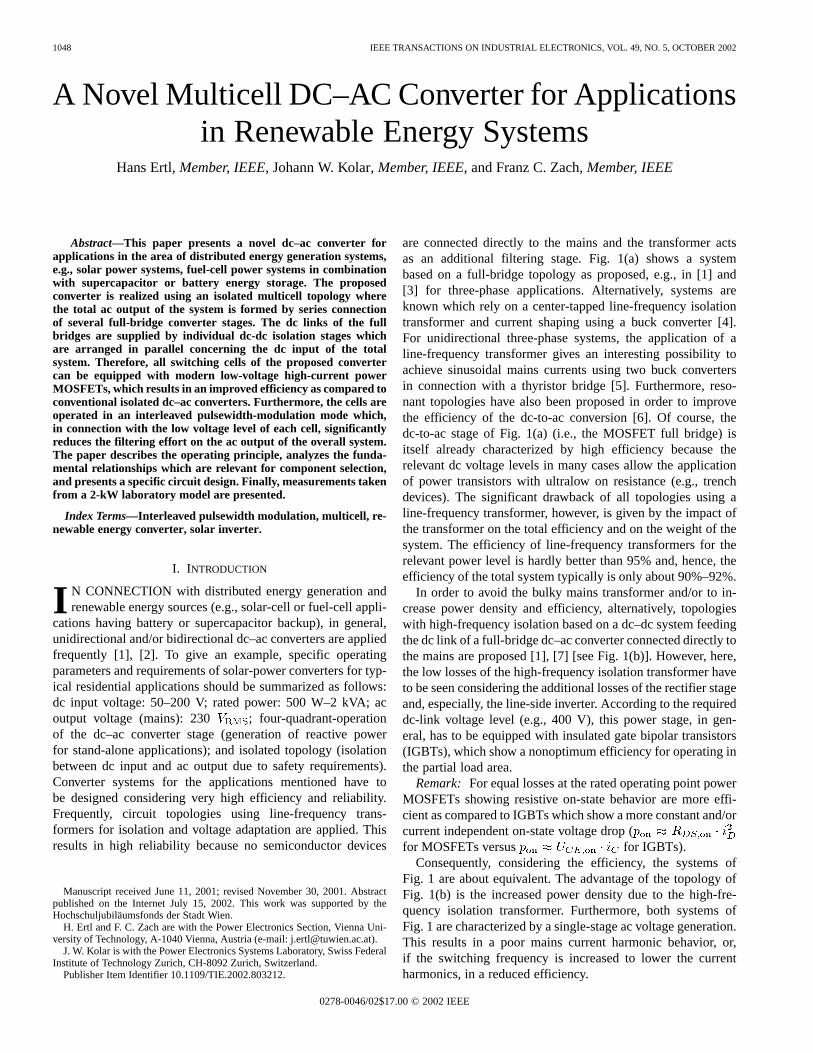
are connected directly to the mains and the transformer actsas an additional filtering stage. Fig. 1(a) shows a systembased on a full-bridge topology as proposed, e.g., in [1] and[3] for three-phase applications. Alternatively, systems areknown which rely on a center-tapped line-frequency isolationtransformer and current shaping using a buck converter [4].For unidirectional three-phase systems, the application of aline-frequency transformer gives an interesting possibility toachieve sinusoidal mains currents using two buck convertersin connection with a thyristor bridge [5]. Furthermore, reso-nant topologies have also been proposed in order to improvethe efficiency of the dc-to-ac conversion [6]. Of course, thedc-to-ac stage of Fig. 1(a) (i.e., the MOSFET full bridge) isitself already characterized by high efficiency because therelevant dc voltage levels in many cases allow the applicationof power transistors with ultralow on resistance (e.g., trenchdevices). The significant drawback of all topologies using aline-frequency transformer, however, is given by the impact ofthe transformer on the total efficiency and on the weight of thesystem. The efficiency of line-frequency transformers for therelevant power level is hardly better than 95% and, hence, theefficiency of the total system typically is only about 90%–92%.
In order to avoid the bulky mains transformer and/or to in-crease power density and efficiency, alternatively, topologieswith high-frequency isolation based on a dc–dc system feedingthe dc link of a full-bridge dc–ac converter connected directly tothe mains are proposed [1], [7] [see Fig. 1(b)]. However, here,the low losses of the high-frequency isolation transformer haveto be seen considering the additional losses of the rectifier stageand, especially, the line-side inverter. According to the requireddc-link voltage level (e.g., 400 V), this power stage, in gen-eral, has to be equipped with insulated gate bipolar transistors(IGBTs), which show a nonoptimum efficiency for operating inthe partial load area.
Remark: For equal losses at the rated operating point powerMOSFETs showing resistive on-state behavior are more effi-cient as compared to IGBTs which show a more constant and/orcurrent independent on-state voltage drop (for MOSFETs versus for IGBTs).
Consequently, considering the efficiency, the systems ofFig. 1 are about equivalent. The advantage of the topology ofFig. 1(b) is the increased power density due to the high-fre-quency isolation transformer. Furthermore, both systems ofFig. 1 are characterized by a single-stage ac voltage generation.This results in a poor mains current harmonic behavior, or,if the switching frequency is increased to lower the currentharmonics, in a reduced efficiency.
0278-0046/02$17.00 © 2002 IEEE
ERTL et al.: MULTICELL DC–AC CONVERTER FOR APPLICATIONS IN RENEWABLE ENERGY SYSTEMS 1049
(a)
(b)
Fig. 1. Basic circuit topology of a solar-powered converter with (a) MOSFET full-bridge and line-frequency isolation transformer and, alternatively, (b) topologywith MOSFET dc-dc converter (high-frequency isolation transformer) with subsequent single-cell IGBT four-quadrant dc–ac converter.
II. M ULTICELL CONVERTER—BASIC CONCEPT
Influenced by the recent developments in the area oflow-voltage power MOSFETs, a converter topology is pro-posed for the application in residential renewable energysystems which originally is known from high-power applica-tions. Multicell multilevel converter systems have been wellknown for many years for high-voltage/high-power applicationsin order to reduce the required blocking voltage of the powersemiconductor devices. For example, fully static 50 Hz-to-162/3 Hz inverters for feeding railway overhead lines [8], con-verters for input current shaping and traction of locomotives[9], in general, for feeding medium- and high-voltage inductionmachines [10]–[12], as well as for static var compensators[13], [14], and also as a utility interface for medium-powerrenewable energy systems [15] have been reported.
Considering modern low-voltage power MOSFETs and inte-grated gate driver stages, however, multicell topologies have be-come attractive, even for converters in the lower power region.The applicability of low-cost standard power components de-signed for high-volume applications (automotive, telecommuni-cation, etc.) overcomes the main drawback of such systems, i.e.,the high number of switching devices. By application of multi-level multicell topologies, the drawbacks of the converter struc-tures discussed in Section I can be avoided, resulting in compactunits with high overall efficiency. There, the key specificationsof the developed residential converter system are as follows:
dc input voltage V (80–120 V);ac output voltage ;rated power kW;efficiency at rated power;high-frequency isolation stage;low-voltage MOSFETs (majority carrier devices).
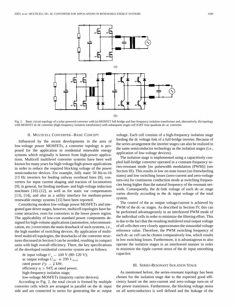
According to Fig. 2, the total circuit is formed by multipleconverter cells which are arranged in parallel on the dc inputside and are connected in series for generating the ac output
voltage. Each cell consists of a high-frequency isolation stagefeeding the dc voltage link of a full-bridge inverter. Because ofthe series arrangement the inverter stages can also be realized inthe same semiconductor technology as the isolation stages (i.e.,application of low-voltage devices).
The isolation stage is implemented using a capacitively cou-pled half-bridge converter operated in a constant-frequency se-ries-resonant mode [no pulsewidth modulation (PWM)] (seeSection III). This results in low on-state losses (no freewheelingstates) and low switching losses (zero-current and zero-voltageturn-on) for continuous conduction mode at switching frequen-cies being higher than the natural frequency of the resonant net-work. Consequently, the dc-link voltage of each dc–ac stagevaries directly according to the dc input voltage of the totalsystem.
The control of the ac output voltage/current is achieved byPWM of the dc–ac stages. As described in Section IV, this canbe performed advantageously in an interleaved PWM mode ofthe individual cells in order to minimize the filtering effort. Thisis due to the fact that the resulting multilevel total output voltageof all cells then very closely approximates the sinusoidal voltagereference value. Therefore, the PWM switching frequency ofeach dc–ac cell can be chosen comparatively low, which resultsin low switching losses. Furthermore, it is advantageous to alsooperate the isolation stages in an interleaved manner in orderto minimize the ripple current stress of the dc input smoothingcapacitor.
III. SERIES-RESONANT ISOLATION STAGE
As mentioned before, the series-resonant topology has beenchosen for the isolation stage due to the expected good effi-ciency based on the zero-current and zero-voltage turn-on ofthe power transistors. Furthermore, the blocking voltage stresson all semiconductors is well defined and the leakage of the

1050 IEEE TRANSACTIONS ON INDUSTRIAL ELECTRONICS, VOL. 49, NO. 5, OCTOBER 2002
Fig. 2. Basic circuit topology of the proposed dc–ac multicell converter based on high-frequency resonant-mode dc–dc isolation stages feeding interleavedPWM-mode MOSFET dc–ac cells connected in series on the ac output (N = 4 cells).
transformer contributes to the effective inductance of the reso-nant network [16]. Therefore, different from, for example, trans-formers for flyback converters, a certain amount of leakage isdesirable here. This is also of importance because the couplingcapacitance between primary and secondary should be mini-mized because the proposed multilevel topology is character-ized by a common-mode voltage stress of the converter cellscaused by the interleaved switching of the individual dc–ac con-verter cells; a low coupling capacitance helps to reduce the re-sulting common-mode current. A circuit topology which is notsensitive to transformer leakage is furthermore of advantage be-cause the primary winding of the transformer shall be realizedby application of the “bow winding principle,” i.e., copper wirebows are connected via the printed circuit board (PCB) to formthe primary winding, whereas the secondary windings are ofconventional type. Such a transformer usually shows significantleakage (but low coupling capacitance) and, therefore, is wellsuited for this series mode resonant topology.
A. Analysis of the Stationary Operating Behavior
In the following, the characteristics of the stationary oper-ation shall be calculated analytically. It should be mentionedthat a center-tapped secondary winding is used for the designedconverter, which results in having only a single diode forwardvoltage drop as compared to bridge rectification [Fig. 3(a)].
Remark: For the desired output voltage range of up to 120 V,usually, 400-V diodes would be suitable for center-tapped rec-tification, whereas for bridge rectification 200-V diodes wouldbe sufficient. Although 400-V devices show a higher on-statevoltage than 200-V diodes, the two 200-V devices acting inseries for bridge rectification cannot compete with the single400-V diode of a center-tapped system.
(a)
(b)
(c)
Fig. 3. Circuit diagram of the (a) series-resonant converter and (b), (c)corresponding equivalent circuits.
Here, the bridge rectifier is given only to develop the equiva-lent circuit diagrams of Fig. 3(b) and (c). The system is char-acterized by four different states defined by the polarities ofthe input voltage and of the reflected secondary voltage.Whereas the polarity of is defined by the control circuit, the

ERTL et al.: MULTICELL DC–AC CONVERTER FOR APPLICATIONS IN RENEWABLE ENERGY SYSTEMS 1051
TABLE IOPERATING STATES OF THESERIES-RESONANT CONVERTER
(a) (b)
(c) (d)
Fig. 4. (a) System trajectory and (b) time behavior of the series-resonantconverter. (c), (d) Simplifications valid for�U � U ; i : output current ofthe rectifier [see Fig. 3(b)].
polarity of is given by the direction of the resonant current. The four possible states (A B C D) are listed in
Table I. For state A, voltages and show equal directionand the (small) difference is applied to theLC series circuit. This results in a circular-shaped system tra-jectory around the center point [ , 0] (see thediagram in Fig. 4(a), defines the characteristicimpedance of the resonant network). Because the system oper-ates with a switching frequency above the natural frequency
, the input voltage changes its polarity atinstant 1 due to the turn-off of the high-side transistor before
becomes zero. Consequently, the system transits to state Bwhere the sum causes a high rate of current reduc-tion [see Fig. 4(b)] according to the circular trajectory with thecenter point [ , 0]. At instant 2, the current be-comes negative, the current in the rectifier diodes commutates,and again shows equal (i.e., negative) polarity as(stateC); now [ , 0] is the new center of the trajectory valid untilthe lower power transistor turns off at instant 3 and the systempasses over to state D (center [ , 0]) which completesa full cycle at instant 4.
For the practical realization of the series-resonant converterstage of the proposed system it is of importance that, in general,
is valid; this is caused by the fact that the charac-teristic impedance is defined by the small induc-tance given to a significant extent by the transformer leakage.With this assumption, the system trajectory in good approxima-tion shows the shape of Fig. 4(c), i.e., the current contributionof states B and D to can be neglected [ , Fig. 4(c)].With this and using the conduction angle
(1)
the equations
(2)
and
(3)
can be written according to the geometric relations given byFig. 4(c) and according to the fact that the average value of(i.e., the rectified inductor current ) in the stationary case isdefined by the load current . Evaluation of (3) and rearrangingusing (2) finally leads to
with (4)
and
(5)
These equations state that, for a given switching frequency(fixed conduction interval ), the output voltage decreasesproportional to the load current , i.e., the converter showsa quasi-ohmic output impedance (current-independent outputresistance ; see equivalent circuit given in Fig. 5).
Remark: This system behavior is very similar to the com-mutation voltage drop of line commutated converters where thecommutation inductances finally cause a current-proportionaloutput voltage reduction.
An exact calculation as given in [17] results in an output char-acteristic described by ellipses (see the thin curves in Fig. 5).However, as is indicated by the shaded area of Fig. 5, for theoperating region being relevant for the proposed system (
) the simplified calculation given here shows excellent ac-curacy. Fig. 6 demonstrates that the output impedance isapproximately linearly dependent on the switching frequencyand for is valid. Therefore, the desired stiffoutput characteristic suggests . However, this wouldlead to a worse transient response (voltage overshoot) because

1052 IEEE TRANSACTIONS ON INDUSTRIAL ELECTRONICS, VOL. 49, NO. 5, OCTOBER 2002
Fig. 5. Output characteristic of the series-resonant converter forfixed-frequency operation above the natural frequency.
Fig. 6. Dependency of the output impedanceR and of the capacitor peakvoltage valueu on the switching frequency.
also acts as damping resistor for the resonant circuit givenby the output inductance (not shown in the equivalent diagramof Fig. 5) and the output smoothing capacitor. Furthermore, ithas to be taken into account that the turn-off of the power tran-sistors has to be performed at ; only in this case thereexists a remaining current which charges the drain-source ca-pacitance of the transistors in order to get zero-voltage turn-on.For a practical realization the resonant network typically is di-mensioned to achieve (i.e., ).
B. Practical Design and Realization
Concerning the design of the multicell converter with thekey specifications as given at the beginning of Section II (ratedpower 2 kW in a four-cell arrangement) the specifications of thedc–dc isolation stage are defined by the following:
dc input voltage V (80–120 V);dc output voltage (1:1 transfer ratio);
Fig. 7. Transformer of the resonant 500-W dc–dc converter using “bowwinding” technique (shown here forN = 4) for direct PCB mounting andcomponents of the coil former.
rated power W;switching frequency – kHz.
For the two power MOSFETs the SiliconMAX devicesPSMN035-150P (TO220 type package, 150 V, 35 m) havebeen chosen. The gate drive is realized using an IR2113 drivercircuit with additional turn-off speedup using two p-n-p transis-tors BC327 to enhance the discharge of the MOSFET gate. Thecenter tapped rectifier on the secondary side of the transformeris equipped with an MUR1640 (2 8 A, 400 V) diode.
The power transformer is, as already mentioned at the begin-ning of Section III, realized by application of the “bow windingprinciple,” i.e., the primary winding is formed bycopper bows ( mm) on the selected E42/21/20 ferrite core(material: N87). The secondary windings ( turnsto get a 1:1 voltage transfer ratio of the converter, mm)are implemented using conventional winding techniques. A coilformer of specific shape (see Fig. 7) is applied to get a compacttransformer design and to guarantee the required creepage andclearance distances. The dimensioning data given before causea peak flux density of mT resulting in core losses of
W at ( V, kHz, C)as specified by the data sheet. Although the proposed windingtechnique does not show very tight coupling, the stray induc-tance of the transformer is too low and a small additional choke(five turns of litz wire on a single ETD29 leg (half core set))has to be used for adjusting the natural frequency of the reso-nant circuit to kHz. With the applied resonance capaci-tors (2 5 0.1 F polyester-foil-type components in parallel,
F) for kHz this results in
H
V at A

ERTL et al.: MULTICELL DC–AC CONVERTER FOR APPLICATIONS IN RENEWABLE ENERGY SYSTEMS 1053
(a)
(b)
Fig. 8. (a) Measured voltage and current wave shapes and (b) measuredsystem trajectory of the laboratory prototype of the series-resonant dc–dcconverter; parameters:U = 120 V, f = 125 kHz, andP � 440 W.
using the equations of Section III. Concerning , it has tobe noted that specifies the output impedance related to theprimary side of the transformer; this value has to be multipliedby for characterizing the output(load-side) behavior of the converter.
C. Laboratory Prototype System—Measurements
The measurements (see Fig. 8) taken from the laboratorymodel show a close correspondence to the theoretical waveshapes as given in Fig. 4 with the exception that the real systemshows a significant reverse-recovery current Aof the rectifier diodes; this matches also with the datasheetspecifications of MUR1640 for A s. The lossmeasurements demonstrate an efficiency of 96.3% at ratedpower (500 W) for 110-kHz switching frequency (Fig. 9). Thepartial load region is characterized by efficiency values up to97%. It has to be noted that the rectifier diodes contribute toabout up to 50% of the total losses. This suggests the applica-tion of synchronous rectification circuit extensions as will be
Fig. 9. Measured losses and efficiency of the prototype dc–dc isolation stage;parameters:U = 120 V.
proposed in Section V. Furthermore, the switching losses couldbe optimized by implementation of a load-dependent interlockdelay time of the driver stage or, alternatively, by applicationof a driver stage with inherent turn-on capability(according to the dual-thyristor principle as described in [17])to achieve true zero-voltage switching within the entire loadregion.
IV. M ULTICELL DC–AC CONVERTER
For the description of the dc–ac converter for generating the230- ac output of the system, one should refer to a large ex-tent to the analyses of the multi-cell class-D switch-mode am-plifier presented in [18]. It has to be pointed out that the essen-tial benefit of the multicell topology is that, if the individualswitching cells are operated in an interleaved PWM mode, theoutput current ripple is reduced by a factor of . By applica-tion of a second-orderLC output filter, the output voltage rippleacross the filtering capacitor is reduced by according to [18,eqs. (5) and (6)], i.e., for the ripple is reduced by afactor of 64 as compared to a single-cell topology, e.g., given inFig. 1(b). This makes it possible to operate the system at a com-paratively low PWM switching frequency. For the realized pro-totype system, a single-cell switching frequency of kHzhas been chosen. Due to the 1:1 voltage transfer ratio of thedc–dc converter the power stages of the dc–ac converter canbe equipped with the same type of power MOSFETs as usedfor the isolation stage ( pieces of PSMN035-150P150-V/35-m devices).
A. PWM Pattern Generation
The pattern generation for the interleaved PWM is performedby a circuit showing remarkably low effort (see [18, Fig. 7 ]).First, a simple CD4047 IC oscillator generates the basic clock(4 ) of the modulator. Subsequently, a “tree” of six toggleflip-flops (three pieces of CD4013) forms four interleavedrectangular signals feeding the inputs of four analog integratorstages realized by a single TL084 operational amplifier IC.At the integrator outputs four phase-shifted triangular signals

1054 IEEE TRANSACTIONS ON INDUSTRIAL ELECTRONICS, VOL. 49, NO. 5, OCTOBER 2002
appear which define the carrier signals for the total of eightcomparators (two pieces of LM339). These devices act as aPWM stage comparing the carrier signals with the referencesignals (i.e., in this case, a 50-Hz sinusoidal signal)of the output voltage. The LM339 ICs directly drive eightsimple low-cost optocouplers (SFH606) which are used toprovide the required isolation between the PWM generatorand the (floating) driver stages of the switching cells. Interlocktiming and gate drive of the power MOSFETs of a half-bridgearrangement is performed using eight standard integrateddriver ICs (IR2111). The auxiliary supply of these devicesis provided by small 0.5-W standard dc–dc converters. Thewhole PWM pattern generation, control, and gate drive of thedc–ac converter fits on a single 160100-mm PCB usingstandard (non-SMD) components. The power consumption ofthe total board (including driver stages) has been measured tobe 1.8 W.
B. Output Filter—Voltage Control
The presented prototype system has been designed for stand-alone applications only and not for feeding energy to the publicmains. For the latter application, the voltage is defined by themains and the converter would have to be equipped with anoutput current control to ensure a voltage-proportional mainscurrent of corresponding amplitude. For stand-alone applica-tions, the output voltage is defined by the PWM control ofthe converter. In the simplest case—as implemented for the re-alized laboratory setup—an open-loop control can be applied.However, with this, the damping of theLC output filter has tobe performed exclusively by the impedance of the load. If apure ohmic load characteristic is guaranteed, asufficient damping is achieved if is valid for thecharacteristic impedance of the LC filter. For
(i.e., output power 2000 W at V )filter components of mH and F have been se-lected resulting in a cutoff frequency of kHz and a char-acteristic impedance of . However, in the case ofno-load or light-load operation or for reactive load, this load-based damping fails and an additional damping branch (e.g., a
-series snubber arranged in parallel to the filter capac-itor , typical values: , ) would be re-quired leading to additional losses appearing in the dampingbranch (i.e., in ). The drawback of the reduced efficiencyof this solution can be avoided if an “active” damping of theLCoutput filter is performed. Implementing a negative feedback ofthe filter capacitor current to the reference voltage input of thePWM stage (feedback coefficient ) gives the desired shiftof the poles of theLC filter to the left side of the plane (see[18]). Choosing, e.g., results in a Butterworthresponse of the system.
However, as indicated by [18, Fig. 10] even for active filterdamping the output voltage quality is low if nonlinear loads(e.g., diode-bridge rectifiers) are supplied. Analysis of the low-frequency harmonics give a total harmonic distortion (THD)
7% of for a diode-bridge rectifier load according to thefollowing parameters: mH, mF, A;
A, ( W, VA, and). This behavior is originated by the output impedance of the
(a)
(b)
Fig. 10. (a) AC output voltage (u : before filtering;u : afterLC outputfilter having a cutoff frequency of� 2 kHz) and (b) output filter inductor currenti of the dc–ac converter laboratory prototype; parameter:f = 1 kHz.
LC filter which can be lowered very much using a closed-loopcontrol of the total output voltage. Using a simple proportional-plus-integral (PI)-type controller reduces the output harmonicsfor the load mentioned before to a THD of2%. A detailed de-scription of the dimensioning of the controller is given in [18,Sec. IV] and shall be omitted here for the sake of brevity. Moresophisticated results would be achievable if a multiloop control(e.g., current control with superimposed output voltage controland feed-forward of the load current) is applied.
C. Laboratory Prototype System—Measurements
The measurement results of the prototype system illustratethe multilevel voltage generation of this multicell topology [seeconverter output voltage in Fig. 10(a)]. The ripple ofthe current through the output filter inductor shows “nodes”being typical for a multilevel approach [Fig. 10(b)]. Across thefilter capacitor there appears the very smooth ac output voltage
of the system. As indicated by the Fourier analysis of theunfiltered output voltage (Fig. 11), significant harmonic

ERTL et al.: MULTICELL DC–AC CONVERTER FOR APPLICATIONS IN RENEWABLE ENERGY SYSTEMS 1055
Fig. 11. Frequency components of theunfiltered converter output voltageu . The harmonics in the frequency range 100–700 Hz are due toa nonideal behavior of the duty-cycle limiting stage which is required toguarantee the operation of the charge pump of the IR2111 driver.
Fig. 12. Efficiency and losses of the dc–ac converter. The characteristicsshown by the dashed curves give an approximation based on an ideal 230-Vvoltage source with 0.75- output resistance and 1.8-W permanent no-loadlosses. Furthermore, the diagram demonstrates the sensitivity to measurementerrors, especially for very-high-efficiency values because the dashed curve inany case defines an upper limit for the efficiency.
components exist only in the vicinity of multiples of 2 , i.e.,for kHz, here, in the vicinity of 8 kHz, 16 kHz, etc., dueto the cancellation of all lower frequency components accordingto the interleaved PWM mode.
As indicated by Fig. 12, the dc–ac converter shows the ex-pected excellent efficiency due to the low of the powertransistors in connection with the almost negligible switchinglosses. However, it has to be noted that the accurate measure-ment of the losses of ultraefficient converters requires very pre-cise testing equipment; even very low measurement errors showa serious impact on the resulting efficiency/loss characteristicof the tested converter. In particular, for the case where proto-types of different systems are tested using different measure-ment equipment, the measurements and the comparison of theresults should be performed very carefully.
V. CONCLUSIONS ANDFUTURE DEVELOPMENTS
With the proposed multicell multilevel converter topology,energy conversion to the mains voltage level (230 is
(a)
(b)
Fig. 13. Extension of the resonance-mode dc–dc converter to (a) synchronousrectification and (b) to bidirectional operation.
possible using exclusively MOSFETs with comparativelylow-rated voltage. These devices are characterized by a verylow on-state voltage drop which results in low conductionlosses. Due to the interleaved switching of the individual cells,the output voltage ripple of the total system is small and, there-fore, good mains behavior (i.e., low mains current harmonics)can be achieved although the PWM of a single cell is basedon a low switching frequency (causing only low switchinglosses). Consequently, the converter shows very high efficiency.Because the voltage control of the system is performed byPWM of the dc–ac converter, the dc–dc converter being re-quired for feeding the floating dc–ac stages can be realized byapplication of an uncontrolled fixed-frequency series-resonanttopology. Equal MOSFET devices can be applied for the dc–dcstage and for the dc–ac converter because of similar voltagelevels of the design used. The high quantity of required powersemiconductor devices (e.g., 24 transistors plus 12 half-bridgedriver circuits for the designed 2-kW prototype) might be seenas a drawback of the proposed topology. However, on the otherhand, this does allow the application of low-cost standardpower semiconductors; the low total losses distributed to ahigh number of power transistors (i.e., the more uniform heatdistribution) significantly simplifies the system cooling. Todemonstrate this circumstance, it should be mentioned that theprototype dc–ac converter can be operated at 50% of the ratedpower (i.e., at 1 kW)without any heat sink.
As mentioned in Section III, concerning future developmentsit would be of interest to apply synchronous rectification to thedc–dc isolation stages because the on-state losses of the diodescontribute considerably to the total system losses. In this case,however, it would be preferable to change to a full-bridge circuitas shown in Fig. 13(a) due to the improved efficiency caused bythe basic physical characteristics of the majority of carrier-basedsemiconductors (in theory, ) and to allow the

1056 IEEE TRANSACTIONS ON INDUSTRIAL ELECTRONICS, VOL. 49, NO. 5, OCTOBER 2002
Fig. 14. Application of the multicell topology to nonisolated solar convertersystems.
application of transistors of the same type for the input andoutput sections of the converter. In principle, the converter ofFig. 13(a) also permits a bidirectional power flow. This opera-tion mode would be of interest if the system is utilized for super-capacitor or battery-based systems (e.g., uninterruptable powersupplies, power flow equalizer systems, etc.) to recharge the en-ergy storage device on the dc input. It should be mentioned thatthe dc–ac converter using the proposed multicell arrangementitself intrinsically permits a full four-quadrant operation. (Thisis of special importance also for reactive power generation ifthe system is used for stand-alone applications not being con-nected to the mains.) However, the converter of Fig. 13(a) doesprovide a dc current path on the secondary which might resultin saturation of the core. This can be avoided by application of
a secondary-side blocking capacitor, or, alternatively, by split-ting up the resonance capacitor to both transformer windings asshown in Fig. 13(b).
Finally, the multicell converter topology should also be pro-posed for nonisolated solar power systems as shown in principlein Fig. 14. Despite the fact that the solar panels show signifi-cant common-mode voltages (which have to be lowered by cur-rent-compensated input chokes) and that a relatively complexcontrol is required to achieve low ac harmonics also for differentdc input voltages with maximum power point (MPP) tracking,this topology could gain attention due to its ultrahigh efficiency.This multicell structure might also be of interest for the realiza-tion of “distributed” power photovoltaic converters.
REFERENCES
[1] C. F. Nayar, S. M. Islam, and H. Sharma, “Power electronics for renew-able energy sources,” inPower Electronics Handbook, M. H. Rashid,Ed. New York: Academic, 2001, ch. 23.
[2] N. Mohan, T. M. Undeland, and W. P. Robbins,Power Electronics, 2nded. New York: Wiley/Academic, 1995, ch. 17-4.
[3] R. L. Steigerwald, A. Ferraro, and G. F. Turnbull, “Application ofpower transistors to residential and intermediate rating photovoltaicarray power conditioners,”IEEE Trans. Power Electron., vol. 19, pp.254–267, Mar./Apr. 1983.
[4] K. H. Edelmoser and F. A. Himmelstoss, “Analysis of a new high-effi-ciency DC-to-AC inverter,”IEEE Trans. Power Electron., vol. 14, pp.454–459, May 1999.
[5] R. Naik and N. Mohan, “A novel grid interface for photovoltaic, wind-electric and fuel-cell systems with a controllable power factor of opera-tion,” in Proc. IEEE APEC’95, vol. 2, 1995, pp. 995–998.
[6] R. Tymerski, V. Voperian, and F. C. Lee, “DC-to-AC inversion usingquasiresonant techniques,”IEEE Trans. Power Electron., vol. 4, pp.381–390, Oct. 1989.
[7] B. K. Bose, P. M. Szczesny, and R. L. Steigerwald, “Microcomputercontrol of a residential photovoltaic power conditioning system,”IEEETrans. Ind. Applicat., vol. 21, pp. 1182–1191, Sept./Oct. 1989.
[8] H. Stemmler, “Power electronics in electric traction applications,” inProc. IEEE IECON’93, vol. 2, 1993, pp. 707–713.
[9] A. C. Rufer, N. Schibli, and Ch. Briguet, “A direct coupled 4-quadrantmultilevel converter for 16(2/3) Hz traction systems,” inProc. 6th Int.Conf. Power Electronics and Variable Speed Drives, Nottingham, U.K.,Sept. 23–25, 1996, pp. 448–453.
[10] N. P. Schibli, T. Nguyen, and A. C. Rufer, “A three-phase multilevel con-verter for high-power induction motors,”IEEE Trans. Power Electron.,vol. 13, pp. 978–986, Sept. 1998.
[11] A. Rufer, M. Veenstra, and G. Gopakumar, “Asymmetric multilevel con-verter for high resolution voltage phasor generation,” inProc. 8th Eur.Conf. Power Electronics and Applications (EPE), Lausanne, Switzer-land, Sept. 7–9, 1999, CD-ROM.
[12] L. M. Tolbert, F. Z. Peng, and T. G. Habetler, “Multilevel converters forlarge electric drives,”IEEE Trans. Ind. Applicat., vol. 33, pp. 36–44,Jan./Feb. 1999.
[13] F. Z. Peng, J.-S. Lai, J. W. McKeever, and J. VanCoevering, “A multi-level voltage-source inverter with separate DC sources for static var gen-eration,”IEEE Trans. Ind. Applicat., vol. 32, pp. 1130–1138, Sept./Oct.1996.
[14] Y. Liang and C. O. Nwankpa, “A new type of STATCOM based oncascading voltage-source inverters with phase-shifted unipolar SPWM,”IEEE Trans. Ind. Appl., vol. 35, pp. 1118–1123, Sept./Oct. 1999.
[15] L. M. Tolbert and F. Z. Peng, “Multilevel converters as a utility interfacefor renewable energy systems,” inProc. IEEE-PES Summer Meeting,Seattle, WA, July 15–20, 2000, pp. 1271–1274.
[16] R. L. Steigerwald, “A comparison of half-bridge resonant convertertopologies,” IEEE Trans. Power Electron., vol. 3, pp. 174–182, Apr.1988.
[17] Y. Cheron, T. Meynard, and C. Goodman,Soft Commutation. London,U.K.: Chapman & Hall/Kluwer Academic, 1992.
[18] H. Ertl, J. W. Kolar, and F. C. Zach, “Analysis of a multi-level multi-cellswitch-mode power amplifier employing the “flying-battery” concept,”IEEE Trans. Ind. Electron., vol. 49, pp. 816–823, Aug. 2002.

ERTL et al.: MULTICELL DC–AC CONVERTER FOR APPLICATIONS IN RENEWABLE ENERGY SYSTEMS 1057
Hans Ertl (M’93) was born in Mauerkirchen,Austria, in 1957. He received the Dipl.-Ing. (M.Sc.)and Ph.D. degrees in industrial electronics from theUniversity of Technology Vienna, Vienna, Austria,in 1984 and 1991, respectively.
Since 1984, he has been with the Universityof Technology Vienna, where he is currently anAssistant Professor in the Power Electronics Section.He has performed various industrial researchprojects in the areas of field-oriented control ofac drive systems, switch-mode power supplies for
welding and industrial plasma processes, and active rectifier systems. He isthe author or coauthor of numerous scientific papers and patents. His currentresearch activities are focused on switch-mode power amplifiers and multicelltopologies, in particular, for the generation of testing signals, for active ripplecurrent compensators, and for several applications in the area of renewableenergy systems.
Johann W. Kolar (M’89) was born in Vöcklabruck,Austria, in 1959. He received the Ph.D. degree(summa cum laude) in industrial electronics from theUniversity of Technology Vienna, Vienna, Austria,in 1998.
Since 1984, he has been with the University ofTechnology in Vienna, where he has been teachingand conducting research in close collaborationwith the industry in the fields of high-performancedrives, high-frequency inverter systems for processtechnology, and uninterruptible power supplies. He
has proposed numerous novel converter topologies, e.g., the Vienna rectifierconcept. He has authored more than 100 scientific papers published in interna-tional journals and conference proceedings and has filed 45 patents. He wasappointed as a Professor at the Swiss Federal Institute of Technology (ETH)Zurich, Zurich Switzerland, in 2001. He is also currently the Head of the PowerElectronics Systems Laboratory. The focus of his current research is on novelconverter topologies with low effects on the mains, e.g., for power supply oftelecommunication systems and distributed power systems in connection withfuel cells. A further main area of research is the realization of ultracompactintelligent converter modules employing the latest power semiconductortechnology (SiC) and novel concepts for cooling and EMC filtering. He isa member of the technical program committees of numerous internationalconferences in the field (e.g., Director of the Power Quality Branch of theInternational Conference on Power Conversion and Intelligent Motion).
Dr. Kolar is a member of the Institute of Electrical Engineers of Japan. Since1997, he has served as an Associate Editor of the IEEE TRANSACTIONS ON
INDUSTRIAL ELECTRONICS.
Franz C. Zach (M’83) was born in Vienna, Austria,in 1942. He received the Dipl.-Ing. (M.Sc.) degreein electrical engineering (telecommunications)and the Ph.D. degree (cum laude) in the area ofautomatic control optimization from the Universityof Technology Vienna, Vienna, Austria, in 1965 and1968, respectively.
From 1965 to 1969, he was a Scientific Assistantwith the University of Technology Vienna and, from1969 to 1972, he was with the NASA Goddard SpaceFlight Center, Greenbelt, MD, where he developed
new optimization methods for attitude control of earth-orbiting satellites. In1972, he became an Associate Professor and then Professor of Power Electronicsat the University of Technology Vienna, where he has headed the Power Elec-tronics Section since 1974. He is the author of numerous technical and scientificpapers and patents and of two books concerning automatic control and powerelectronics. His current activities are in the area of power electronics and asso-ciated controls, in particular, as used for power supplies and electrical drives.