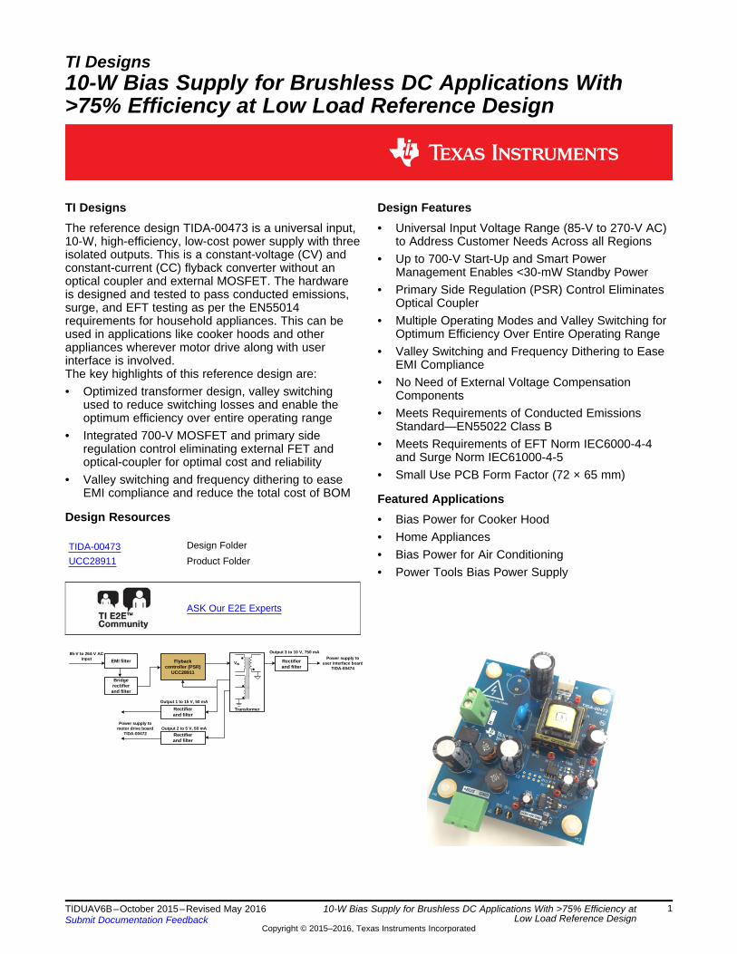
TI Designs - 10-W Bias Supply for Brushless DC Applications ...
38
EMI filter Bridge rectifier and filter 85-V to 264-V AC input Flyback controller (PSR) UCC28911 Rectifier and filter Output 3 to 10 V, 750 mA Transformer Power supply to user interface board TIDA-00474 Power supply to motor drive board TIDA-00472 Output 1 to 15 V, 50 mA Output 2 to 5 V, 50 mA Rectifier and filter Rectifier and filter VIN 1 TIDUAV6B – October 2015 – Revised May 2016 Submit Documentation Feedback Copyright © 2015–2016, Texas Instruments Incorporated 10-W Bias Supply for Brushless DC Applications With >75% Efficiency at Low Load Reference Design TI Designs 10-W Bias Supply for Brushless DC Applications With >75% Efficiency at Low Load Reference Design TI Designs The reference design TIDA-00473 is a universal input, 10-W, high-efficiency, low-cost power supply with three isolated outputs. This is a constant-voltage (CV) and constant-current (CC) flyback converter without an optical coupler and external MOSFET. The hardware is designed and tested to pass conducted emissions, surge, and EFT testing as per the EN55014 requirements for household appliances. This can be used in applications like cooker hoods and other appliances wherever motor drive along with user interface is involved. The key highlights of this reference design are: • Optimized transformer design, valley switching used to reduce switching losses and enable the optimum efficiency over entire operating range • Integrated 700-V MOSFET and primary side regulation control eliminating external FET and optical-coupler for optimal cost and reliability • Valley switching and frequency dithering to ease EMI compliance and reduce the total cost of BOM Design Resources TIDA-00473 Design Folder UCC28911 Product Folder ASK Our E2E Experts Design Features • Universal Input Voltage Range (85-V to 270-V AC) to Address Customer Needs Across all Regions • Up to 700-V Start-Up and Smart Power Management Enables <30-mW Standby Power • Primary Side Regulation (PSR) Control Eliminates Optical Coupler • Multiple Operating Modes and Valley Switching for Optimum Efficiency Over Entire Operating Range • Valley Switching and Frequency Dithering to Ease EMI Compliance • No Need of External Voltage Compensation Components • Meets Requirements of Conducted Emissions Standard—EN55022 Class B • Meets Requirements of EFT Norm IEC6000-4-4 and Surge Norm IEC61000-4-5 • Small Use PCB Form Factor (72 × 65 mm) Featured Applications • Bias Power for Cooker Hood • Home Appliances • Bias Power for Air Conditioning • Power Tools Bias Power Supply
-
Upload
khangminh22 -
Category
Documents
-
view
7 -
download
0
Transcript of TI Designs - 10-W Bias Supply for Brushless DC Applications ...
EMI filter
Bridgerectifierand filter
85-V to 264-V ACinput Flyback
controller (PSR)UCC28911
Rectifierand filter
Output 3 to 10 V, 750 mA
Transformer
Power supply touser interface board
TIDA-00474
Power supply tomotor drive board
TIDA-00472
Output 1 to 15 V, 50 mA
Output 2 to 5 V, 50 mA
Rectifierand filter
Rectifierand filter
VIN
1TIDUAV6B–October 2015–Revised May 2016Submit Documentation Feedback
Copyright © 2015–2016, Texas Instruments Incorporated
10-W Bias Supply for Brushless DC Applications With >75% Efficiency atLow Load Reference Design
TI Designs10-W Bias Supply for Brushless DC Applications With>75% Efficiency at Low Load Reference Design
TI DesignsThe reference design TIDA-00473 is a universal input,10-W, high-efficiency, low-cost power supply with threeisolated outputs. This is a constant-voltage (CV) andconstant-current (CC) flyback converter without anoptical coupler and external MOSFET. The hardwareis designed and tested to pass conducted emissions,surge, and EFT testing as per the EN55014requirements for household appliances. This can beused in applications like cooker hoods and otherappliances wherever motor drive along with userinterface is involved.The key highlights of this reference design are:• Optimized transformer design, valley switching
used to reduce switching losses and enable theoptimum efficiency over entire operating range
• Integrated 700-V MOSFET and primary sideregulation control eliminating external FET andoptical-coupler for optimal cost and reliability
• Valley switching and frequency dithering to easeEMI compliance and reduce the total cost of BOM
Design Resources
TIDA-00473 Design FolderUCC28911 Product Folder
ASK Our E2E Experts
Design Features• Universal Input Voltage Range (85-V to 270-V AC)
to Address Customer Needs Across all Regions• Up to 700-V Start-Up and Smart Power
Management Enables <30-mW Standby Power• Primary Side Regulation (PSR) Control Eliminates
Optical Coupler• Multiple Operating Modes and Valley Switching for
Optimum Efficiency Over Entire Operating Range• Valley Switching and Frequency Dithering to Ease
EMI Compliance• No Need of External Voltage Compensation
Components• Meets Requirements of Conducted Emissions
Standard—EN55022 Class B• Meets Requirements of EFT Norm IEC6000-4-4
and Surge Norm IEC61000-4-5• Small Use PCB Form Factor (72 × 65 mm)
Featured Applications• Bias Power for Cooker Hood• Home Appliances• Bias Power for Air Conditioning• Power Tools Bias Power Supply

Key System Specifications www.ti.com
2 TIDUAV6B–October 2015–Revised May 2016Submit Documentation Feedback
Copyright © 2015–2016, Texas Instruments Incorporated
10-W Bias Supply for Brushless DC Applications With >75% Efficiency at LowLoad Reference Design
An IMPORTANT NOTICE at the end of this TI reference design addresses authorized use, intellectual property matters and otherimportant disclaimers and information.
1 Key System Specifications
Table 1. Electrical Performance Specifications
PARAMETER SYMBOL TEST CONDITIONS MIN NOM MAX UNITINPUT CHARACTERISTICSInput voltage VIN 85 115/230 270 VACFrequency fLINE 47 50/60 64 HzNo load power PNL Vin = 90 V Iout = 0 A 40 mWBrownout voltage VIN_UVLO IOUT = INOM 75 VBrownout recoveryvoltage VINOV 85 V
Input current IINVIN =VMINIOUT = IOUT(MAX)
0.25 A
OUTPUT CHARACTERISTICS
Primary outputvoltage
VOUT1
VIN =VMIN to VMAXIOUT = 0 to INOM
4.5 5 5.5
VVOUT2 14.5 15Secondary outputvoltage VOUT3 9.5 10 10.5
Maximum outputcurrent
IOUT1(MAX)
VIN =VMIN to VMAX
50mAIOUT2(MAX) 50
IOUT3(MAX) 750
Minimum outputcurrent
IOUT1(MIN)
VIN = VMIN to VMAX
5mAIOUT2(MIN) 0
IOUT3(MIN) 10Line regulation ± 1 %Load regulation ± 5 %
Output voltage rippleΔVOUT1 VIN = VMIN to VMAX 70
mVΔVOUT2 IOUT1, IOUT2, IOUT3 = 0 to INOM 80ΔVOUT3 150
Total maximumoutput power POUT VIN = VMIN to VMAX 8.5 W
Insulation class Test from primary to secondaryReinforce
dinsulation
SYSTEM CHARACTERISTICS
Efficiency ηVIN =VNOMIOUT = 25%, 50%, 75%, 100% ofIOUT
75 80 83 %
Protection
Output overpowerOutput overvoltageInput UVLOThermal shutdown
Operation ambient T Open frame -40 25 65 °C
Conductedemissions
Test with TIDA-00472Or test individual
As perEN55022 – class
B
EFT Tested with TIDA-00472 As per IEC-61000-4-4
Surge Tested with TIDA-00472 As per IEC-61000-4-5

www.ti.com Key System Specifications
3TIDUAV6B–October 2015–Revised May 2016Submit Documentation Feedback
Copyright © 2015–2016, Texas Instruments Incorporated
10-W Bias Supply for Brushless DC Applications With >75% Efficiency atLow Load Reference Design
Table 1. Electrical Performance Specifications (continued)PARAMETER SYMBOL TEST CONDITIONS MIN NOM MAX UNIT
MECHANICAL
DimensionsW Width 72
mmL Length 65H Component height 20

System Description www.ti.com
4 TIDUAV6B–October 2015–Revised May 2016Submit Documentation Feedback
Copyright © 2015–2016, Texas Instruments Incorporated
10-W Bias Supply for Brushless DC Applications With >75% Efficiency atLow Load Reference Design
2 System DescriptionHome appliance equipment use different subsystems for the proper functionality, such as motor drives,lighting systems, user interfaces, and so on. Air conditioners, washing machines, refrigerator, dishwashers, and kitchen hoods are examples of such home appliances. A properly rated and protected biaspower supply is required for gate drivers, microcontrollers, LED lighting and interface, user interface, andso on used in these subsystems.
The TIDA-00473 reference design is primarily aiming to power kitchen hood (also called range vent hood,range hood, cooker hood, or chimney) subsystems. The cooker hood consists of a suction fan driven by amains powered electric motor, lamps, and human interface or control options. The advanced cooker hooduses the efficient brushless DC (BLDC) motor drives. The BLDC motor drive uses gate drivers andmicrocontrollers, which need different regulated bias supplies such as 15 V, 3.3 V, 5 V, and so on for theirfunctionality. LED lighting is another subsystem in kitchen hood, which needs a regulated low-voltage DCpower supply with enough power rating to drive the LEDs. The user interface such as touch keys orproximity sensing also consists of microcontrollers and sensors that need a regulated low-voltage DCpower supply.
The TIDA-00473 is a reference bias power supply design for kitchen hoods. However, it is applicable inany other systems where a bias power supply needs to be generated from the high voltage mains. TheTIDA-00473 is designed meet the universal input voltage range of 85-V to 270-V AC. The design providesthree isolated outputs: 15 V for the gate driver used in the motor drive, 5 V for the microcontroller in themotor drive, and 10 V for the LED drive and user interface. The TIDA-00473 is a CV and CC flybackconverter without an optical coupler and external MOSFET.
Valley switching technique reduces switching losses, and the controller consumption is dynamicallyadjusted with load, which can enable the optimum efficiency over the entire operating range. Theintegrated 700-V MOSFET and primary side regulation control eliminates the external FET and opticalcoupler for optimal cost and reliability. Valley switching and frequency dithering eases EMI complianceand reduces the total cost of the BOM.
The hardware is designed and tested to pass conducted emissions, surge, and EFT testing as per theEN55014 requirements for household appliances.

EMI filter
Bridgerectifierand filter
85-V to 264-V ACinput Flyback
controller (PSR)UCC28911
Rectifierand filter
Output 3 to 10 V, 750 mA
Transformer
Power supply touser interface board
TIDA-00474
Power supply tomotor drive board
TIDA-00472
Output 1 to 15 V, 50 mA
Output 2 to 5 V, 50 mA
Rectifierand filter
Rectifierand filter
VIN
www.ti.com Block Diagram
5TIDUAV6B–October 2015–Revised May 2016Submit Documentation Feedback
Copyright © 2015–2016, Texas Instruments Incorporated
10-W Bias Supply for Brushless DC Applications With >75% Efficiency atLow Load Reference Design
3 Block Diagram
Figure 1. Block Diagram of Power Supply With Isolated Multiple Outputs
3.1 Highlighted Products and Key AdvantagesThe following subsections detail the highlighted products used in this reference design, including the keyfeatures for their selection. See their respective product datasheets for complete details.
3.1.1 UCC28911—Flyback Controller (Primary Side Regulation)The UCC28911 is high-voltage flyback switcher that provides output voltage and current regulation withoutthe use of an optical coupler. This device incorporate a 700-V power FET and a controller that processoperating information from the flyback auxiliary winding and power FET to provide a precise output voltageand current control. The integrated high-voltage current source for startup is switched off during operation,and the controller current consumption is dynamically adjusted with the load. This controller can enable avery low standby power consumption.
Control algorithms in the UCC28911, combining switching frequency and peak primary current modulation,allow operating efficiencies to meet or exceed applicable standards. Discontinuous conduction mode(DCM) with valley switching reduces switching losses. Built-in protection features help to keep secondaryand primary component stress levels in check across the operating range. The frequency jitter helps toreduce EMI filter cost.
Low system parts count and built-in advanced protection features result in a cost-effective solution thatmeets stringent world-wide energy efficiency requirements.
The UCC28911 also has a complete set of system protection features that greatly improve reliability andfurther simplifies the design:• Input undervoltage lockout• Output overvoltage protection• Output overpower protection• Primary overcurrent• VDD clamp overcurrent• Thermal shutdown

System Design Theory www.ti.com
6 TIDUAV6B–October 2015–Revised May 2016Submit Documentation Feedback
Copyright © 2015–2016, Texas Instruments Incorporated
10-W Bias Supply for Brushless DC Applications With >75% Efficiency atLow Load Reference Design
4 System Design TheoryThis reference design is a universal input, 10-W power supply with three isolated outputs designed forbias power of appliances. The power supply is configured as a CV and CC flyback converter using theUCC28911 controller. The UCC28911 is a high voltage switcher that integrates a high voltage power FETand a primary-side-regulated controller, supporting magnetically-sensed output voltage regulation throughthe transformer bias winding. This type of sensing eliminates the need for a secondary-side reference,error amplifier, and optical isolator for output voltage regulation. The device delivers accurate outputvoltage under static load, load variations, and line voltage variation and provides accurate control of outputcurrent.
The magnetic sampling scheme allows operation only in DCM so the device is not allowed to turn on thepower FET if it does not sense a zero crossing detector (ZCD) event. A ZCD event is when auxiliarywinding voltage crosses zero from high to low after transformer demagnetization is completed. Themodulator adjusts both frequency and peak current in different load regions to maximize efficiencythroughout the operating range. The smart management of the control logic power consumption and thehigh-voltage (HV) current source, used for startup that is off during operation and have very low leakagecurrent, allow designing converters with very low standby input power. The standby input power less than30 mW at90-V AC input can be easily achieved with this device.
4.1 Design RequirementThe design parameters used in this reference design is given in Table 2.
Table 2. Design Parameters
PARAMETER SYMBOL NOTES AND TEST CONDITIONS MIN NOM MAX UNITINPUT CHARACTERISTICS
Input voltage VIN 85 115/230 270 VAC
Frequency fLINE 47 50/60 64 HzNo load power PNL VIN = 90 V IOUT = 0 A 40 mWBrownout voltage VIN_UVLO IOUT = INOM 75 VBrownout recoveryvoltage VINOV 85 V
Input current IINVIN = VMINIOUT = IOUT(MAX)
0.25 A
OUTPUT CHARACTERISTICS
Primary outputvoltage
VOUT1
VIN = VMIN to VMAXIOUT = 0 to INOM
4.5 5 5.5
VVOUT2 14.5 15Secondary outputvoltage VOUT3 9.5 10 10.5
Maximum outputcurrent
IOUT1(MAX)
VIN = VMIN to VMAX
50mAIOUT2(MAX) 50
IOUT3(MAX) 750
Minimum outputcurrent
IOUT1(MIN)
VIN = VMIN to VMAX
5mAIOUT2(MIN) 0
IOUT3(MIN) 10
Output voltage rippleΔVOUT1
VIN = VMIN to VMAXIOUT1, IOUT2, IOUT3 = 0 to INOM
70mVΔVOUT2 80
ΔVOUT3 150Total maximumoutput power POUT VIN = VMIN to VMAX 8.5 W
SYSTEM CHARACTERISTICS
Efficiency η VIN =VNOMIOUT = 25%, 50%, 75%, 100% of IOUT
75 80 83 %

1mHL1
1mHL2
~3
+1
~4
-2
D1
DF06M
1
2
J1
1715721
100k
R8
D4
1N4007
GND1
GND2
GND3
IPK4
VS5
VDD6
DRAIN8
U1 UCC28911D
1
2
J2
1757242
6.8kR1
6.8kR2
10µF
C1
10µF
C2
1
4
9
8
3
5
6
T1
0.1µF
C410µF/25V
C3
170V
D2
SMBJ170A-TR
22.6k
R4
N.I.
R7
61.9k
R6
12R
R3D3
BAV21W-7-F
1
3
2
D7
PDS5100-13
10R
R121000pFC11
0.1µF
C13
6.8k
R13
1
2
J6
43650-0213
47µF/35V
C8
0.1µF
C7
D6
ES1B-13-F
1
2
3
J3
61300311121
0.1µF
C6
1.6k
R10
3.6k
R11
A2
C1
D5
D_SCHOT_DFLS1200
C10
To TIDA-00472
To TIDA-00474
AGND
SGND
470pF
C5
732R
R5
732R
R9
TP3
TP5
TP1
TP4
TP6
TP7
TP8
TP9
TP10
TP2
470µF/10V
C9
TP11
TP12
Q1 BCX 55-16 E6327
470R
R15
15V
ZD1
AGND
0RR14
1k
R17
47µF/35V
C15
6.8k
R16
1000µF
C16
1000µF
C12
Blue
21
D8
www.ti.com System Design Theory
7TIDUAV6B–October 2015–Revised May 2016Submit Documentation Feedback
Copyright © 2015–2016, Texas Instruments Incorporated
10-W Bias Supply for Brushless DC Applications With >75% Efficiency atLow Load Reference Design
4.2 Detailed Design ProcedureThis procedure outlines the steps to design the CV, CC flyback converter based on the UCC28911. SeeFigure 2 for component names and network locations. The design procedure equations use terms that aredefined in Section 4.2.1.
Figure 2. Multiple Output Flyback Converter Based on UCC28911
• Diode bridge D1, input capacitors C1 and C2, transformer T1, UCC28911 switcher U1, Schottkyrectifiers D5, D6, and D7, and capacitors C8, C9, and C16 form the power stage of the converter. Notethat the U1 is also part of the power stage since the high-voltage MOSFET is integrated in U1.
• The input EMI filter is made up of C1 and C2 and differential mode inductors L1 and L2.• R1 and R2 serve the dual function of dampening input filter oscillations and prevent a large voltage
being developed across L1 and L2 in the event of an ESD pulse.• Resistors R5 and R9, capacitor C5, and diode D4 make up the primary side voltage clamp. The clamp
prevents the drain voltage on U1 from exceeding its maximum rating. A secondary function of theclamp is to alleviate the EMI currents associated with the turn-off voltage of U1.
• Operating bias to the controller is provided by the auxiliary winding on T1, diode D3, resistor R3, andbulk capacitor C3.
• Resistor R6 programs the startup voltage threshold.• Resistors R4 and R7 program the output voltage set point.• Resistors R10 and R11 program the maximum output current.• Resistors R13, R16, and R17 adjust the no load output voltage.
( ) ( )
OUT
P 2
TARGET MAXPK
P 2L 0.95 mH
I 1.05 f
´= =
´ ´ ´ h
2
RP
PRMS PK MAX RP
KI = I D - K + 1 = 0.304 A
3
æ öç ÷´ ´ç ÷è ø
SPK
PK
PS
II 0.535 A
N= =
OUT
O1
SPK
P2
VI 4.233 A
0.425
´
= =
( )MIN
PS
O1 D
X
1
MAD VN 7.911
0.425 V V
´= =
´ +
( ) ( ) ( )OUT O1 D1 O1 O2 D2 O2 O3 D3 O3P V V I V V I V V I 8.995 W= + ´ + + ´ + + ´ =
( )MATAR XGET
MAX
f
D 1 0.425 0.000002 0.4952
= - - ´ =
System Design Theory www.ti.com
8 TIDUAV6B–October 2015–Revised May 2016Submit Documentation Feedback
Copyright © 2015–2016, Texas Instruments Incorporated
10-W Bias Supply for Brushless DC Applications With >75% Efficiency atLow Load Reference Design
4.2.1 Transformer DesignDesign specifications:• Maximum input DC voltage: VMAX = 380 V• Minimum start up input DC voltage: VMIN = 120 × 0.6 = 75 V (see Section 4.2.2)• Ripple current to peak current ratio: KRP = 0.4• Output voltage 1): VO1 = 10 V• Output current 1: IO1 = 0.75 A• Diode voltage drop at output 1: VD1 = 0.6 V• Output voltage 2: VO2 = 5 V• Output current 2: IO2 = 0.05 A• Diode voltage drop at output 2: VD2 = 0.5 V• Output voltage 3: VO3 = 15 V• Output current 3: IO3 = 0.05 A• Diode voltage drop at output 3: VD3 = 0.4 V• Maximum switching frequency: fTARGET(MAX) = 80 kHz• Allowed AC flux density (Tesla): BAC = 0.075; BMAX = 0.3
• Maximum duty cycle:• Target Converter efficiency: η = 0.75• Window utilization factor: KU = 0.4• Current density (A/m2): JC = 500 × 104
spaceCalculate the total output power, POUT:
(1)
spaceCalculate transformer primary-to-secondary turns ratio, NPS:
(2)
spaceCalculate the primary peak current, IPK, and the primary RMS current, IPRMS, using the main secondarypeak current, ISPK:
(3)
(4)
(5)
spaceCalculate the primary inductance (H), LP:
(6)

P PKMAX_REAL
P E
L IB 0.284
N A
´
= =
´
( )P O3 D3
S3
MAX MIN
N V V 0.425N 17
D V
´ + ´= =
´
( )P O2 D2
S2
MAX MIN
N V V 0.425N 6
D V
´ + ´= =
´
( )O1P D1
S1
MAX MIN
N V V 0.425N 11
D V
´ + ´= =
´
P PK
P
MAX E
L I 1.05N 88
B A
´ ´
= =
´
( )PRMS PK RP P 12 4
C U AC
2 I I K LAP 10 412.42 mm
J K 2 B
´ ´ ´ ´= ´ =
´ ´ ´
www.ti.com System Design Theory
9TIDUAV6B–October 2015–Revised May 2016Submit Documentation Feedback
Copyright © 2015–2016, Texas Instruments Incorporated
10-W Bias Supply for Brushless DC Applications With >75% Efficiency atLow Load Reference Design
Calculate the area product (mm4), AP:
(7)
Select a proper core from core database according to AP, Select the Core size is EE16, and the real APvalue is APREAL = 801 mm4.
spaceCalculate the primary winding turns, NP:
(8)
spaceCalculate the three output winding turns, NS1, NS2, and NS3:
(9)
(10)
(11)
spaceCalculate the real maximum flux density, BMAX_REAL:
(12)
Because BMAX_REAL < BMAX, this transformer will not saturate even at the worst case.

BULK 2 2
2 10.625 1 1 75arccos
47 2 2 120C 18.3 F
2 85 75
æ ö´ æ ö´ - ´ç ÷ç ÷´ p è øè ø= = m´ -
IN BULK(MIN)
LINE(MIN) IN(MIN)
BULK 2 2IN(MIN) BULK(MIN)
2 P V1 1arccos
f RCT 2 2 VC
2 V V
æ öæ ö´ç ÷ç ÷´ - ´
ç ÷ç ÷´ p ´è øè ø=´ -
OUT1 OUT1 OUT2 OUT2 OUT3 OUT3
IN
IN
V I V I V IP
5 0.05 15 0.05 10 0.75P 10.625 W
0.8
´ + ´ + ´=
h
´ + ´ + ´= =
System Design Theory www.ti.com
10 TIDUAV6B–October 2015–Revised May 2016Submit Documentation Feedback
Copyright © 2015–2016, Texas Instruments Incorporated
10-W Bias Supply for Brushless DC Applications With >75% Efficiency atLow Load Reference Design
4.2.2 Selecting Input Bulk CapacitanceThe minimum input capacitance voltage, the input power of the converter based on target full-loadefficiency, minimum input RMS voltage, and minimum AC input frequency determine the input capacitancerequirement.
The maximum converter input power can be estimated from the output voltage in the CV mode (VOCV), theconverter's output current when operating in CC mode (IOCC), and the full-load target efficiency (η).
(13)
Equation 14 provides an accurate solution for input capacitance based on a target minimum bulk capacitorvoltage (VBULK(MIN)). To target a given input capacitance value, iterate the minimum capacitor voltage toachieve the target capacitance.
(14)
As shown in Figure 2, the reference design has a full wave bridge rectifier at the input. The voltageVBULK(MIN) is generally selected around 65% to 60% of √2 × VIN(MIN). With these considerations:
Taking into account that electrolytic capacitance with 10% of tolerance, the values selected for C1 and C2are: C1 = C2 = 10 µF.
The maximum DC bus voltage is 380 V. Therefore, a 400-V/450-V capacitor is a good choice.

2200 F 5 V 3.4 mAC3 16.6 F
0.75 A 3 V
m ´ ´= = m
´
OUT OCC RUN(MAX)VDD
OCC UVLO
C V IC
I V
´ ´=
´ D
( )TRAN
out SW(MIN)
I 750 mAC16 1786 F
V f 10 9 420D
= = = m´ - ´
www.ti.com System Design Theory
11TIDUAV6B–October 2015–Revised May 2016Submit Documentation Feedback
Copyright © 2015–2016, Texas Instruments Incorporated
10-W Bias Supply for Brushless DC Applications With >75% Efficiency atLow Load Reference Design
4.2.3 Selecting Output CapacitanceThe output capacitor value is typically determined by the transient response requirement from no load (forexample, to maintain a minimum output voltage of 9 V with a load-step transient from 0 to 750 mA (ITRAN)).Equation 15 assumes that at no load the converter is operating at the minimum switching frequency(fSW(MIN)).
(15)
A margin of 20% is added to the output capacitance, so the values selected for C16 is 2200 µF.
4.2.4 VDD Capacitance for UCC28911The capacitance on VDD of the UCC28911 needs to supply the device operating current until the output ofthe converter reaches the target minimum operating voltage in CC regulation. At this time, the auxiliarywinding can sustain the supply voltage. The output current available to the load to charge the outputcapacitors is the CC regulation target. Equation 16 assumes the output current of the flyback is availableto charge the output capacitance until the minimum output voltage is achieved. In Figure 2, C3 is providedas the VDD capacitor.
(16)
Where• ΔVUVLO is UVLO hysteresis, equal to VDDON – VDDOFF
• IRUN(MAX) is supply current required at VDD
The ΔVUVLO and IRUN(MAX) can be found in the datasheet of the UCC28911 (SLUS769). In this referencedesign, the values are selected as ΔVUVLO = 3 V, IRUN(MAX) = 3.4 mA .
Substituting the values in Equation 16,
(17)
10 µF is selected for C3, which is the nearest low value capacitor compared to 16.6 µF, to ensure a lowstart-up time.

BRIDGE F _BRIDGE IN_ AVG(MAX)P 2 V I 2 0.8 0.187 0.299 W= ´ ´ = ´ ´ =
( )IN_ AVG(MAX) IN MAX
2 2I I 0.294 0.187 A= ´ = ´ =
p p
( ) ( )IN MAX IN_RMS MAXI 2 I 2 0.208 0.294 A= ´ = ´ =
( )( )
IN
IN_RMS MAXIN MIN
P 10.625I 0.208 A
V PF 85 0.6= = =
´ ´
System Design Theory www.ti.com
12 TIDUAV6B–October 2015–Revised May 2016Submit Documentation Feedback
Copyright © 2015–2016, Texas Instruments Incorporated
10-W Bias Supply for Brushless DC Applications With >75% Efficiency atLow Load Reference Design
4.2.5 Bridge RectifierThe maximum input AC voltage is 270-V AC, so the DC voltage can reach voltage levels of up to 385-VDC. Considering a safety factor of 30%, select a component with voltage rating greater than 500-V DC.The input bridge rectifier must have an average current capability that exceeds the input average current(IIN_AVG(MAX)). To optimize the power loss due to the diode forward voltage drop, a bridge rectifier with highercurrent rating is recommended.
To get the IIN_AVG(MAX), first calculate the maximum input RMS line current, IIN_RMS(MAX).
(18)
Based upon the calculated RMS values, the maximum input current, IIN(MAX), and the maximum averageinput current, IIN_AVG(MAX), can be determined by assuming the waveform is sinusoidal, as shown inEquation 19 and Equation 20:
(19)
(20)
Considering the operating environment temperature and current margin, select DF06M for the D1. Theforward voltage drop of DF06M is VF_BRIDGE = 0.8 V.
Therefore, the power loss in the input bridge, PBRIDGE, can be calculated as:
(21)

( ) ( )4.05 76.8 5.17
R4 25.54k10 0.5 8 4.05 5.17
´ ´= =
+ ´ - ´
( ) ( )VSR PA
OUT F PS VSR PA
V R6 NR4
V V N V N
´ ´=
+ ´ - ´
75 2R6 78.77k
5.17 260 A
´= =
´ m
( )
IN_UVLO
PA VSLRUN MAX
V 2R6
N I
´=
´
tLK_RESET
tSMPL
VS Ring p-p
tDMAG
www.ti.com System Design Theory
13TIDUAV6B–October 2015–Revised May 2016Submit Documentation Feedback
Copyright © 2015–2016, Texas Instruments Incorporated
10-W Bias Supply for Brushless DC Applications With >75% Efficiency atLow Load Reference Design
4.2.6 Output Voltage Set PointThe UCC28911 VS Signal Discriminator Block ensures an accurate sampling time for an accurate sampleof the output voltage from the auxiliary winding. However, there are some details of the auxiliary windingsignal to ensure reliable operation, specifically the reset time of the leakage inductance and the duration ofany subsequent leakage inductance ring.
Figure 3. VS Voltage
The first detail to examine is the duration of the leakage inductance reset pedestal, tLK_RESET. Because thiscan mimic the waveform of the secondary current decay, followed by a sharp down-slope, keep theleakage reset time less than 500 ns for IDRAIN minimum, and less than 1.5μs for IDRAIN maximum. Thesecond detail is the amplitude of ringing on the auxiliary winding waveform (VAUX) following tLK_RESET. Thepeak-to-peak voltage at the VS pin should be less than approximately 100mVp-p at least 200 ns beforethe end of the demagnetization time, tDMAG. If there is a concern with excessive ringing, it usually occursduring light or no-load conditions when tDMAG is at the minimum. The tolerable ripple on VS is scaled up tothe auxiliary winding voltage by R6 and R4 and is equal to 100 (R6 + R4) / R4 mV. So the VS dividerresistors determine the output voltage regulation point of the flyback converter. Also, the high-side dividerresistor (R6) determines the line voltage at which the controller enables continuous switching operation.R6 is initially determined based on transformer auxiliary to primary turn ratio and desired input voltageoperating threshold.
(22)
Where IVSLRUN(MAX) is the VS line sense run current (found in the datasheet of UCC28911)., The typicalvalue of IVSLRUN(MAX) is 260 µA, so
In this reference design, the selected value of R6 is 76.8k. The low-side VS pin resistor R4 is selectedbased on desired output voltage regulation.
(23)
Where VVSR is the regulating level of VS pin (found in the datasheet of UCC28911). Usually, the typicalvalue of VVSR is 4.05 V.
In this reference design, the selected values of R4 and R7 are 27k and 510k, respectively.

IN(MAX)REV OUT
PS
V 2 270 2V V 1.5 10 1.5 86 V
N 8
æ ö´ æ ö´ç ÷= + ´ = + ´ =ç ÷ç ÷ç ÷ è øè ø
IPK
640R 1.12k
0.521 110%= =
´
( )( )CSTE MAX
D _PK MAXIPK
VI
R=
System Design Theory www.ti.com
14 TIDUAV6B–October 2015–Revised May 2016Submit Documentation Feedback
Copyright © 2015–2016, Texas Instruments Incorporated
10-W Bias Supply for Brushless DC Applications With >75% Efficiency atLow Load Reference Design
4.2.7 Output Power Set PointA resistance (RIPK) connected between IPK pin and GND sets the maximum value of the power FET peakcurrent, ID_PK(MAX). A current, ISENSE, proportional to the power FET current, comes out from the IPK pinduring power FET on time. The voltage across RIPK is fed to the PWM comparator and establishes toswitch off the power FET according to Equation 24:
(24)
Where VCSTE(MAX) is the equivalent current sense threshold, which can be found in the datasheet ofUCC28911. From that datasheet, the maximum value of VCST(MAX) is 640 V at a VVS of 3.75 V. If the IPK pinis shorted to GND (RIPK = 0), the peak current is automatically set to ID_PEAK(MAX), 700 mA for UCC28911.
A test is performed at device start-up to check whether the IPK pin is shorted to GND or the RIPK ispresent. If RIPK is less than maximum RIPK_SHORT, the device interprets it as a short (RIPK = 0) and theDRAIN peak current is set to ID_PEAK(MAX). Otherwise, if RIPK is greater than minimum RIPK(MIN) , the devicesets the DRAIN peak current according to Equation 24. A value of RIPK that is in between the before saidvalues are not allowed since the value of the peak current may be selected using either of the two senseresistances: the internal sense resistance and RIPK.
In this reference, the R10 and R11 can be calculated by Equation 25:
(25)
Considering the accuracy and environmental implication, place a margin of 10%, so the selected value ofR10 and R11 are 1.6k and 3.6k.
4.2.8 Output Rectifier Diode SelectionThe maximum reverse voltage that the secondary diode had to sustain can be calculated by Equation 26where a margin of 50% is considered. Usually for this kind of application, a Schottky diode reduces thepower losses due to the lower forward voltage drop. The maximum current rating of the diode is generallyselected between two to five times the maximum output current (IOCC).
(26)
In this reference design, the PDS5100-13 (100-V, 5-A Schottky) is selected as the secondary rectifierdiode D7.
LKPLR5 2
C5> ´
D4
1N4007
1
3
732RR5
100k
R8470pFC5
732RR9
2
2
3 6
10R13 16.28k
1 0.5210.97 10 420 7 190 10
2 3
- -
= =æ ö
´ ´ ´ ´ - ´ ´ç ÷è ø
( )( )
( ) ( )
2OUT
PRL 2
D _PK MAX
P SW MIN OFF WAITQ MINAM
MIN
VR
I1L f VDD I
2 K
=æ öç ÷´ ´ ´ - ´ç ÷è ø
www.ti.com System Design Theory
15TIDUAV6B–October 2015–Revised May 2016Submit Documentation Feedback
Copyright © 2015–2016, Texas Instruments Incorporated
10-W Bias Supply for Brushless DC Applications With >75% Efficiency atLow Load Reference Design
4.2.9 Pre-Load CalculationWhen no load is applied on the converter output, the output voltage rises until the overvoltage protection(OVP) of the device is tripped, because the device cannot operate at zero switching frequency. Thedevice's minimum switching frequency of 420 Hz will always deliver some energy to the output, causingthe voltage to rise at no load. To avoid this, an RPRL (pre-load resistance) must be used. The value of thispre-load can be selected using the following equation:
(27)
where• KAM is AM control ratio, KAM = VCSE(MAX) / VCSE(MIN) (found in datasheet of UCC28911)• IWAITQ(MIN) is quiescent wait supply current; in the UCC28911 datasheet, this is usually set as 190 µA• VDDOOF(MIN) is VDD turn-off threshold (found in datasheet of UCC28911)
So in this reference design, the pre-load resistance can be calculated by:
In this reference design, the selected value of R13 is 6.8k.
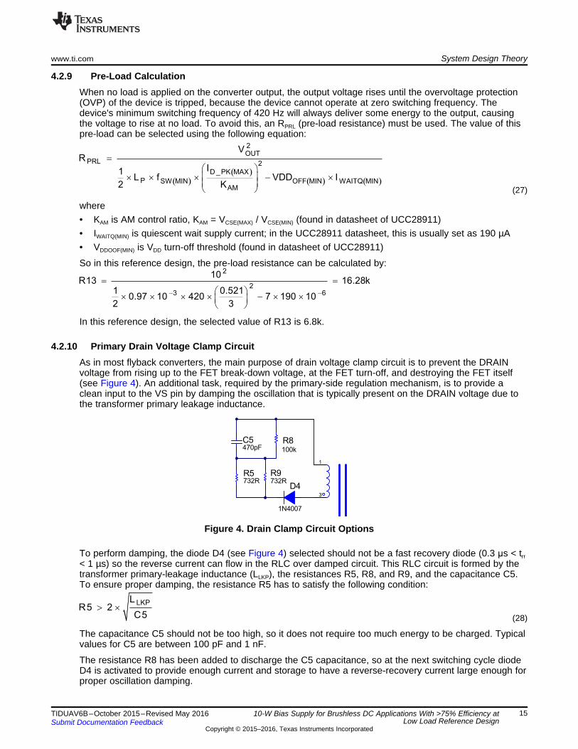
4.2.10 Primary Drain Voltage Clamp CircuitAs in most flyback converters, the main purpose of drain voltage clamp circuit is to prevent the DRAINvoltage from rising up to the FET break-down voltage, at the FET turn-off, and destroying the FET itself(see Figure 4). An additional task, required by the primary-side regulation mechanism, is to provide aclean input to the VS pin by damping the oscillation that is typically present on the DRAIN voltage due tothe transformer primary leakage inductance.
Figure 4. Drain Clamp Circuit Options
To perform damping, the diode D4 (see Figure 4) selected should not be a fast recovery diode (0.3 μs < trr< 1 µs) so the reverse current can flow in the RLC over damped circuit. This RLC circuit is formed by thetransformer primary-leakage inductance (LLKP), the resistances R5, R8, and R9, and the capacitance C5.To ensure proper damping, the resistance R5 has to satisfy the following condition:
(28)
The capacitance C5 should not be too high, so it does not require too much energy to be charged. Typicalvalues for C5 are between 100 pF and 1 nF.
The resistance R8 has been added to discharge the C5 capacitance, so at the next switching cycle diodeD4 is activated to provide enough current and storage to have a reverse-recovery current large enough forproper oscillation damping.

TIDA-00473
Electronic loads
Output 1: 5 V Output 2: 15 V Output 3: 10 V
GND
Power meter
AC source
Multimeter
L N
V_HI V_LO A_HI A_LO
Getting Started: Hardware www.ti.com
16 TIDUAV6B–October 2015–Revised May 2016Submit Documentation Feedback
Copyright © 2015–2016, Texas Instruments Incorporated
10-W Bias Supply for Brushless DC Applications With >75% Efficiency atLow Load Reference Design
5 Getting Started: Hardware
5.1 Test ConditionsFigure 5 shows the basic test setup recommended for evaluating the TIDA-00473 during no load and fullload. During the no load test, set the power analyzer for long averaging to include several cycles ofoperation and an appropriate current scale factor should be used.
For input, the AC source (VIN) must range from 50-V to 270-V AC. Set the Input current limit of input ACsource to 1 A. For output, use an electronic variable load or a variable resistive load, which must be ratedfor ≥ 400 V and vary the load current from 0 mA to 1 A.
Figure 5. Test Environment Setup Recommended
5.2 Equipment Needed• Isolated AC source: The input source must be an isolated variable AC source capable of supplying
between 50-V and 270-VRMS at no less than 25 W and connected as shown in Figure 5. For accurateefficiency calculations, insert a power meter between the AC source and the TIDA-00473. For highestaccuracy, connect the voltage terminals of the power meter directly across the power source.(Connecting the voltage terminals directly to the TIDA-00473 will result in a small current error which issignificant when measuring no load power.)
• Loads: Use a programmable electronic loads with three outputs set to constant resistance mode andcapable of sinking 0 to 1-A DC at 20-V DC.
• Power meter: The power analyzer is capable of measuring low input current, typically less than 100µA, and a long averaging mode if input power measurements of the low-power standby mode are to betaken. An example of such an analyzer is the Yokogawa WT210 Digital Power Meter. To measure theintermittent bursts of current and power drawn from the line during no-load operation, set the WT210 tointegrate.
• Multimeter: Digital multimeters measure the regulated output voltages (DMM V1, DMM V2, and DMMV3) and load current (DMM A1, DMM A2, and DMM A3).
• Oscilloscope: A digital or analog oscilloscope with a 100-MHz scope probe is recommended.• Recommended wire gauge: a minimum of AWG 24-wire is recommended. The wire connections
between the AC source and the TIDA-00473 and the wire connections between the reference designboard and the load should be less than two feet long.

www.ti.com Getting Started: Hardware
17TIDUAV6B–October 2015–Revised May 2016Submit Documentation Feedback
Copyright © 2015–2016, Texas Instruments Incorporated
10-W Bias Supply for Brushless DC Applications With >75% Efficiency atLow Load Reference Design
5.3 Test ProcedureThe following test procedure is recommended primarily for powering up and shutting down the TIDA-00473. Never leave a powered TIDA-00473 evaluated board unattended for a long time.
5.3.1 Applying Power to the TIDA-00473
1. Set up the TIDA-00473 evaluated board as shown in Figure 5.(a) If no load input power measurements are to be made, set the power analyzer to long averaging or
integrating power measurement mode.(b) For operation with a load, as shown in Figure 5, set the electronic load to constant resistance
mode. Adjust the resistance setting in the electronic load for changing the load.2. Prior to turning on the AC source, set the voltage to between 85-V and 270-V AC.3. Turn on the AC source.4. Monitor the output voltage on DMM V1, V2, and V3
5. Monitor the output current on DMM A1, A2, and A3
5.3.2 Output Voltage Regulation and Efficiency
1. For load regulation:(a) Use the test setup shown in Figure 5.(b) Set the AC source to a constant voltage between 85-V and 265-V AC.(c) Apply power to the TIDA-00473 per Section 5.3.1.(d) Vary the load current from 0 A up to 0.75 A.
2. For line regulation:(a) Set the load to sink full load.(b) Vary the AC source from 85-V to 265-V AC.
3. Make sure the input power is off and the bulk capacitor and output capacitors are completelydischarged before handling the TIDA-00473 evaluated board.
5.3.3 Equipment Shutdown
1. Ensure the load is at maximum; this will quickly discharge the output capacitors.2. Turn off the AC source.3. Make sure the bulk capacitors and output capacitors are completely discharged before handling the
TIDA-00473 evaluated board.

Test Results www.ti.com
18 TIDUAV6B–October 2015–Revised May 2016Submit Documentation Feedback
Copyright © 2015–2016, Texas Instruments Incorporated
10-W Bias Supply for Brushless DC Applications With >75% Efficiency at LowLoad Reference Design
6 Test ResultsThe test results are divided in multiple sections that cover the steady state performance measurements,functional performance waveforms and test data, transient performance waveforms, thermalmeasurements, conducted emission measurements, and surge and EFT measurements.
6.1 Performance Data
6.1.1 Cross Regulation With Load VariationTable 3 shows the cross regulation data at 230-V AC input, where the data V15A means 15-V voltagemonitored after the LDO circuit (at TP6), and the V15B means 15-V voltage monitored before LDO circuit(across C8).
Table 3. Cross Regulation With Load Variation at 230-V AC Input
V5 (V) I5 (A) V15A (V) V15B (V) I15 (A) V10 (V) I10 (A)4.65 0 14.28 15.05 0 10.26 04.69 0 14.25 14.95 0 9.81 0.014.94 0 14.39 15.47 0 9.78 0.055.04 0 14.41 15.74 0 9.8 0.15.15 0 14.45 16.06 0 9.81 0.25.27 0 14.46 16.44 0 9.82 0.35.41 0 14.51 16.84 0 9.83 0.45.56 0 14.55 17.3 0 9.84 0.55.72 0 14.59 17.79 0 9.85 0.65.95 0 14.69 18.36 0 9.86 0.754.69 0.05 14.54 16.19 0 11.7 04.66 0.05 14.49 16.1 0 10.81 0.014.67 0.05 14.43 15.57 0 10.01 0.054.75 0.05 14.44 15.52 0 9.81 0.14.83 0.05 14.47 15.83 0 9.8 0.24.9 0.05 14.5 16.14 0 9.82 0.34.96 0.05 14.52 16.47 0 9.83 0.45.01 0.05 14.55 16.81 0 9.84 0.55.06 0.05 14.57 17.15 0 9.84 0.65.15 0.05 14.65 17.52 0 9.86 0.755.01 0 13.75 14.64 0.05 13.01 04.92 0 13.84 14.68 0.05 10.52 0.014.9 0 13.82 14.68 0.05 9.86 0.054.91 0 13.83 14.72 0.05 9.74 0.15.07 0 14.07 15.01 0.05 9.8 0.25.1 0 14.25 15.27 0.05 9.82 0.35.17 0 14.32 15.44 0.05 9.83 0.45.23 0 14.36 15.61 0.05 9.84 0.55.29 0 14.39 15.76 0.05 9.85 0.65.38 0 14.46 15.98 0.05 9.87 0.754.71 0.05 13.91 14.83 0.05 13.4 04.681 0.05 14.02 14.85 0.05 10.77 0.014.7 0.05 13.98 14.81 0.05 9.94 0.054.73 0.05 13.9 14.79 0.05 9.81 0.14.81 0.05 14.07 15 0.05 9.79 0.24.88 0.05 14.21 15.22 0.05 9.82 0.3

www.ti.com Test Results
19TIDUAV6B–October 2015–Revised May 2016Submit Documentation Feedback
Copyright © 2015–2016, Texas Instruments Incorporated
10-W Bias Supply for Brushless DC Applications With >75% Efficiency atLow Load Reference Design
Table 3. Cross Regulation With Load Variation at 230-V AC Input (continued)V5 (V) I5 (A) V15A (V) V15B (V) I15 (A) V10 (V) I10 (A)4.93 0.05 14.29 15.4 0.05 9.83 0.44.98 0.05 14.33 15.56 0.05 9.84 0.55.02 0.05 14.37 15.69 0.05 9.85 0.65.09 0.05 14.45 15.88 0.05 9.87 0.75
6.1.2 Regulation With Line Variation (AC Input)Table 4 shows the data for the line regulation of the output with AC input voltage variation.
Table 4. Regulation With Line Variation at Full Load
INPUTVOLTAGE
(VAC)V5 (V) I5 (A) V15A (V) V15B (V) I15 (A) V10 (V) I10 (A)
90 5.14 0.05 14.51 16.16 0.05 9.84 0.75120 5.14 0.05 14.51 16.11 0.05 9.86 0.75150 5.11 0.05 14.37 16.03 0.05 9.87 0.75180 5.1 0.05 14.45 15.97 0.05 9.87 0.75220 5.08 0.05 14.4 15.89 0.05 9.87 0.75250 5.07 0.05 14.43 15.84 0.05 9.87 0.75270 5.07 0.05 14.36 15.8 0.05 9.87 0.75
Table 5. Regulation With Line Variation at No Load
INPUTVOLTAGE
(VAC)V5 (V) I5 (A) V15A (V) V15B (V) I15 (A) V10 (V) I10 (A)
90 4.69 0 14.26 14.95 0 10.01 0120 4.7 0 14.29 14.95 0 10.03 0150 4.68 0 14.25 14.96 0 10.06 0180 4.68 0 14.29 14.97 0 10.05 0220 4.68 0 14.26 14.98 0 10.06 0250 4.68 0 14.3 14.99 0 10.05 0270 4.68 0 14.28 14.99 0 10.07 0
6.1.3 Standby PowerThe standby power was tested at multiple AC input voltages with only a pre-load on output. The resultsare tabulated in Table 6.
Table 6. No Load Power Measurement
INPUT VOLTAGE (VAC) INPUT CURRENT (mA) STANDBY POWER (mW)90 0.603 30.4120 0.618 34150 0.479 36.8180 0.496 47230 0.449 58270 0.522 73

10-V Load Current (A)
10-V
Out
put (
V)
0 0.1 0.2 0.3 0.4 0.5 0.6 0.7 0.80
2
4
6
8
10
12
14
16
D001
5-V No Load & 15-V No Load5-V Full Load & 15-V No Load5-V No Load & 15-V Full Load5-V Full Load & 15-V Full Load
Test Results www.ti.com
20 TIDUAV6B–October 2015–Revised May 2016Submit Documentation Feedback
Copyright © 2015–2016, Texas Instruments Incorporated
10-W Bias Supply for Brushless DC Applications With >75% Efficiency atLow Load Reference Design
6.1.4 Efficiency TestThe efficiency was tested at 115-V AC and 230-V AC input voltages with full load on output. The resultsare tabulated in Table 7.
Table 7. Efficiency Test at 115-V AC Input
LOAD (%) PIN (W) V5 (V) I5 (A) V15 (V) I15 (A) V10 (V) I10 (A) POUT (W) EFFICIENCY (%)
100 10.31 5.146 0.0499 14.5 0.0505 9.94 0.749 8.43 81.7775 7.85 5.155 0.0375 14.58 0.0375 9.92 0.573 6.42 81.8350 5.25 5.113 0.0249 14.55 0.0255 9.9 0.38 4.26 81.1325 2.65 5.03 0.0124 14.49 0.0125 9.89 0.186 2.08 78.5510 1.12 4.961 0.0049 14.45 0.0055 9.88 0.0754 0.85 75.710 0.04 4.7 0 14.37 0 10.27 0 0 0
Table 8. Efficiency Test at 230-V AC Input
LOAD (%) PIN (w) V5 (V) I5 (A) V15 (V) I15 (A) V10 (V) I10 (A) POUT (w) EFFICIENCY (%)
100 10.19 5.117 0.0499 14.55 0.0505 9.94 0.75 8.45 82.9175 7.76 5.123 0.0375 14.54 0.0375 9.93 0.574 6.44 8350 5.21 5.1 0.0249 14.51 0.0255 9.91 0.38 4.26 81.8225 2.67 5.08 0.0124 14.48 0.0125 9.88 0.185 2.07 77.5710 1.11 5.01 0.0049 14.43 0.0055 9.87 0.0754 0.85 76.410 0.048 4.698 0 14.39 0 10.3 0 0 0
6.2 Performance Curves
6.2.1 Cross Regulation With Load Variation
Figure 6. Cross Regulation at 10-V Output With 5-V and 15-V Load Parameter

Input Voltage (Vac)
10-V
Out
put (
V)
9.5
9.7
9.9
10.1
90 120 150 180 220 250 270
D004
Full LoadNo Load
Input Voltage (Vac)
5-V
Out
put (
V)
4.5
4.7
4.9
5.1
5.3
90 120 150 180 220 250 270
D002
Full LoadNo Load
Input Voltage (Vac)15
-V O
utpu
t (V
)
14
14.2
14.4
14.6
90 120 150 180 220 250 270
D003
Full LoadNo Load
www.ti.com Test Results
21TIDUAV6B–October 2015–Revised May 2016Submit Documentation Feedback
Copyright © 2015–2016, Texas Instruments Incorporated
10-W Bias Supply for Brushless DC Applications With >75% Efficiency atLow Load Reference Design
6.2.2 Regulation With Line Variation (AC Input)
Figure 7. Line Regulation at 5-V Output With Full Loadand No Load
Figure 8. Line Regulation at 15-V Output With Full Loadand No Load
Figure 9. Line Regulation at 10-V Output With Full Load and No Load

Pout (W)
Effi
cien
cy
0 1 2 3 4 5 6 7 8 975%
76%
77%
78%
79%
80%
81%
82%
83%
84%
D005
Vin = 115 VacVin = 230 Vac
Test Results www.ti.com
22 TIDUAV6B–October 2015–Revised May 2016Submit Documentation Feedback
Copyright © 2015–2016, Texas Instruments Incorporated
10-W Bias Supply for Brushless DC Applications With >75% Efficiency atLow Load Reference Design
6.2.3 Efficiency
Figure 10. Efficiency Curves at 115-V AC and 230-V AC Inputs
6.3 Functional Waveforms
6.3.1 VDS Switching Node WaveformsWaveform at switching node (VDS) was observed for 115-V AC and 270-V AC input under full loadconditions.
Figure 11. VDS Waveform at VIN = 270-V AC, Full Load Figure 12. VDS Waveform at VIN = 115-V AC, Full Load
From the test result of the VDS switching waveform, at VIN = 270-V AC (the maximum input voltage), thepeak VDS voltage is only 528-V DC. This voltage is far below of the VDRAIN maximum voltage stress of 700-V DC, so the voltage safety margin is satisfactory.
www.ti.com Test Results
23TIDUAV6B–October 2015–Revised May 2016Submit Documentation Feedback
Copyright © 2015–2016, Texas Instruments Incorporated
10-W Bias Supply for Brushless DC Applications With >75% Efficiency atLow Load Reference Design
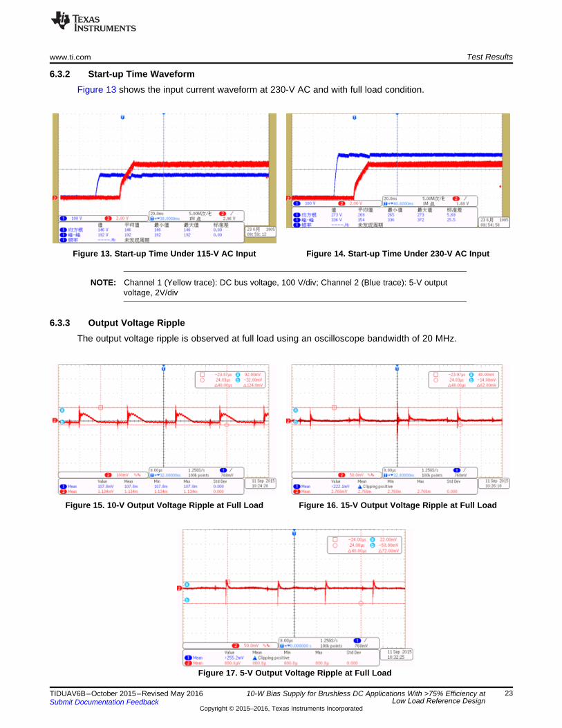
6.3.2 Start-up Time WaveformFigure 13 shows the input current waveform at 230-V AC and with full load condition.
Figure 13. Start-up Time Under 115-V AC Input Figure 14. Start-up Time Under 230-V AC Input
NOTE: Channel 1 (Yellow trace): DC bus voltage, 100 V/div; Channel 2 (Blue trace): 5-V outputvoltage, 2V/div
6.3.3 Output Voltage RippleThe output voltage ripple is observed at full load using an oscilloscope bandwidth of 20 MHz.
Figure 15. 10-V Output Voltage Ripple at Full Load Figure 16. 15-V Output Voltage Ripple at Full Load
Figure 17. 5-V Output Voltage Ripple at Full Load

Test Results www.ti.com
24 TIDUAV6B–October 2015–Revised May 2016Submit Documentation Feedback
Copyright © 2015–2016, Texas Instruments Incorporated
10-W Bias Supply for Brushless DC Applications With >75% Efficiency atLow Load Reference Design
6.4 Transient Waveforms
6.4.1 Transient Load ResponseFor Figure 18 to Figure 20, VIN = 230-V AC, and the load transient goes from no load to full load. Theoutput load is switched using electronic load. Also, the red trace is the output voltage, 20 V/div, ACcoupling, and the green trace is the output current, 1 A/div.
Figure 18. Step Load at 10-V Output (0.1 to 0.75 A) Figure 19. Step Load at 15-V Output (0 to 0.05 A)
NOTE: CH1 (15 V) 0.5 A/div, CH2 (10 V) 0.1 V/div, CH3 (5 V) 0.2 V/div
Figure 20. Step Load 5 V (0 to 0.05 A)
NOTE: CH1 (15 V) 0.1 A/div, CH2 (10 V) 0.1 V/div, CH3 (5 V) 0.2 V/div

www.ti.com Test Results
25TIDUAV6B–October 2015–Revised May 2016Submit Documentation Feedback
Copyright © 2015–2016, Texas Instruments Incorporated
10-W Bias Supply for Brushless DC Applications With >75% Efficiency atLow Load Reference Design
6.5 Conducted EmissionsThe conducted emission test of TIDA-00473 is done at full load condition.
6.5.1 TIDA-00473 Board With Resistive Load at OutputThis test uses 230-V AC inputs with the full load connected to PSU with short leads. The conductedemissions in a pre-compliance test setup were compared against EN55022 class B limits and found tomeet them Comfortably
The conducted emission test uses a pre-compliance meter as per the standard EN55022 class B limit.The test result shows that the board is passing the test with a good margin.
NOTE: The conduction emission results captured in Figure 21 are average and peak. The limitsspecified in the standard are average and quasi-peak.
Figure 21. Conducted Emissions as per EN55022 Class B
Test Results www.ti.com
26 TIDUAV6B–October 2015–Revised May 2016Submit Documentation Feedback
Copyright © 2015–2016, Texas Instruments Incorporated
10-W Bias Supply for Brushless DC Applications With >75% Efficiency atLow Load Reference Design
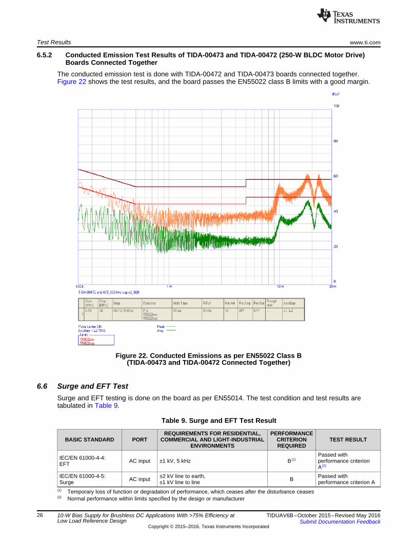
6.5.2 Conducted Emission Test Results of TIDA-00473 and TIDA-00472 (250-W BLDC Motor Drive)Boards Connected Together
The conducted emission test is done with TIDA-00472 and TIDA-00473 boards connected together.Figure 22 shows the test results, and the board passes the EN55022 class B limits with a good margin.
Figure 22. Conducted Emissions as per EN55022 Class B(TIDA-00473 and TIDA-00472 Connected Together)
6.6 Surge and EFT TestSurge and EFT testing is done on the board as per EN55014. The test condition and test results aretabulated in Table 9.
(1) Temporary loss of function or degradation of performance, which ceases after the disturbance ceases(2) Normal performance within limits specified by the design or manufacturer
Table 9. Surge and EFT Test Result
BASIC STANDARD PORTREQUIREMENTS FOR RESIDENTIAL,
COMMERCIAL AND LIGHT-INDUSTRIALENVIRONMENTS
PERFORMANCECRITERIONREQUIRED
TEST RESULT
IEC/EN 61000-4-4:EFT AC input ±1 kV, 5 kHz B (1)
Passed withperformance criterionA (2)
IEC/EN 61000-4-5:Surge AC input ±2 kV line to earth,
±1 kV line to line B Passed withperformance criterion A

www.ti.com Test Results
27TIDUAV6B–October 2015–Revised May 2016Submit Documentation Feedback
Copyright © 2015–2016, Texas Instruments Incorporated
10-W Bias Supply for Brushless DC Applications With >75% Efficiency atLow Load Reference Design
6.7 Thermal MeasurementsThermal image of the board is captured at full load without any external cooling. The board runs for 15minutes before capturing the thermal image.
Test setting 1: Input voltage: 90-V AC, input power: 10.4 W
Figure 23. Top Side Temperatures at 90-V AC, 10.4-W Input Power
Table 10. Temperature at Different Points on Board at 90-V AC, 10.4 W
TEMPERATURE OBSERVED ON TEMPERATUREAmbient 22°CFlyback controller (U1) 65.5°CTransformer (T1) 43.9°COutput diode snubber (R12) 46.1°C

Test Results www.ti.com
28 TIDUAV6B–October 2015–Revised May 2016Submit Documentation Feedback
Copyright © 2015–2016, Texas Instruments Incorporated
10-W Bias Supply for Brushless DC Applications With >75% Efficiency atLow Load Reference Design
Test setting 2: Input voltage: 230-V AC, input power: 10.4 W
Figure 24. Top Side Temperatures at 230-V AC, 10.4-W Input Power
Table 11. Temperature at Different Points on Board at 230-V AC, 10.4 W
TEMPERATURE OBSERVED ON TEMPERATUREAmbient 22.1°CFlyback controller (U1) 54.6°CTransformer (T1) 45.7°COutput diode snubber (R12) 52.8°C

1mHL1
1mHL2
~3
+1
~4
-2
D1
DF06M
1
2
J1
1715721
100k
R8
D4
1N4007
GND1
GND2
GND3
IPK4
VS5
VDD6
DRAIN8
U1 UCC28911D
1
2
J2
1757242
6.8kR1
6.8kR2
10µF
C1
10µF
C2
1
4
9
8
3
5
6
T1
0.1µF
C410µF/25V
C3
170V
D2
SMBJ170A-TR
22.6k
R4
N.I.
R7
61.9k
R6
12R
R3D3
BAV21W-7-F
1
3
2
D7
PDS5100-13
10R
R121000pFC11
0.1µF
C13
6.8k
R13
1
2
J6
43650-0213
47µF/35V
C8
0.1µF
C7
D6
ES1B-13-F
1
2
3
J3
61300311121
0.1µF
C6
1.6k
R10
3.6k
R11
A2
C1
D5
D_SCHOT_DFLS1200
C10
To TIDA-00472
To TIDA-00474
AGND
SGND
470pF
C5
732R
R5
732R
R9
TP3
TP5
TP1
TP4
TP6
TP7
TP8
TP9
TP10
TP2
470µF/10V
C9
TP11
TP12
Q1 BCX 55-16 E6327
470R
R15
15V
ZD1
AGND
0RR14
1k
R17
47µF/35V
C15
6.8k
R16
1000µF
C16
1000µF
C12
Blue
21
D8
www.ti.com Design Files
29TIDUAV6B–October 2015–Revised May 2016Submit Documentation Feedback
Copyright © 2015–2016, Texas Instruments Incorporated
10-W Bias Supply for Brushless DC Applications With >75% Efficiency at LowLoad Reference Design
7 Design Files
7.1 SchematicsTo download the schematics, see the design files at TIDA-00473.
Figure 25. TIDA-00473 Schematic
space
space
space
space
space
space
space
space
space

Design Files www.ti.com
30 TIDUAV6B–October 2015–Revised May 2016Submit Documentation Feedback
Copyright © 2015–2016, Texas Instruments Incorporated
10-W Bias Supply for Brushless DC Applications With >75% Efficiency at LowLoad Reference Design
7.2 Bill of MaterialsTo download the bill of materials (BOM), see the design files at TIDA-00473.
Table 12. BOM
QTY REFERENCE PART DESCRIPTION MANUFACTURER MANUFACTURERPARTNUMBER NOTE
1 PCB1 Printed Circuit Board Any TIDA-00473 Fitted2 C1, C2 CAP, AL, 10 µF, 400 V, +/- 20%, ohm, TH Nichicon UCY2G100MPD1TD Not Fitted2 C12, C16 CAP, AL, 1000 µF, 25 V, +/- 20%, ohm, TH Nichicon UPM1E102MHD6 Fitted1 C3 CAP, AL, 10 µF, 35 V, +/- 20%, TH Nichicon UVR1V100MDD1TA Fitted2 C8, C15 CAP, AL, 47 µF, 35 V, +/- 20%, TH Nichicon UVZ1V470MDD Fitted1 C9 CAP, AL, 470 µF, 10 V, +/- 20%, TH Nichicon UPW1A471MPD Fitted
1 C4 CAP, CERM, 0.1 µF, 25 V, +/- 10%, X5R,0603 AVX 06033D104KAT2A Fitted
1 C5 CAP, CERM, 470 pF, 630 V, +/- 5%,C0G/NP0, 1206 TDK C3216C0G2J471J Fitted
3 C6, C7, C13 CAP, CERM, 0.1 µF, 50 V, +/- 5%, X7R, 0805 AVX 08055C104JAT2A Fitted
1 C10 CAP, CERM, 1000 pF, 250 V, +/- 20%, E,Radial Disc D10.5x7mm TDK CS11-E2GA102MYNS Fitted
1 C11 CAP, CERM, 1000 pF, 500 V, +/- 10%, X7R,1206_190 Kemet C1206C102KCRACTU Fitted
1 D1 Diode, Switching-Bridge, 600 V, 1 A, TH Diodes Inc. DF06M Not Fitted1 D2 Diode, TVS, Uni, 170 V, 600 W, SMB STMicroelectronics SMBJ170A-TR Not Fitted1 D3 Diode, Switching, 200 V, 0.2 A, SOD-123 Diodes Inc. BAV21W-7-F Fitted1 D4 Diode, Rectifier, 1000 V, 1 A, SMA ON Semiconductor MRA4007T3G Fitted1 D5 Diode, Schottky, 1A, 200V Diodes DFLS1200 Fitted1 D6 Diode, Superfast Rectifier, 100 V, 1 A, SMA Diodes Inc. ES1B-13-F Fitted1 D7 Diode, Schottky, 100 V, 5 A, PowerDI5 Diodes Inc. PDS5100-13 Fitted1 D8 LED, Blue, SMD Wurth Elektronik 150060BS75000 Optional4 H1, H4, H7, H10 Bumpon, Hemisphere, 0.44 X 0.20, Clear 3M SJ-5303 (CLEAR) Fitted
4 H3, H6, H9, H12 Machine Screw, Round, #4-40 x 1/4, Nylon,Philips panhead B&F Fastener Supply NY PMS 440 0025 PH Fitted
1 J1 Conn Term Block, 2POS, 5.08mm, TH Phoenix Contact 1715721 Not Fitted
1 J2 Header (Shrouded), 5.08 mm, 2x1, Tin, R/A,TH Phoenix Contact 1757242 Fitted
1 J6 43650-0213 Molex 43650-0213 Fitted1 J3 Header, 2.54 mm, 3x1, Gold, TH Wurth Elektronik 61300311121 Fitted

www.ti.com Design Files
31TIDUAV6B–October 2015–Revised May 2016Submit Documentation Feedback
Copyright © 2015–2016, Texas Instruments Incorporated
10-W Bias Supply for Brushless DC Applications With >75% Efficiency at LowLoad Reference Design
Table 12. BOM (continued)
QTY REFERENCE PART DESCRIPTION MANUFACTURER MANUFACTURERPARTNUMBER NOTE
2 L1, L2 Inductor, Shielded Drum Core, MetalComposite, 1 mH, 0.5 A, 1.7 ohm, TH Wurth Elektronik 768772102 Not Fitted
1 Q1 BCX 55-16 E6327 Infineon Technologies BCX 55-16 E6327 Fitted1 R15 RES, 470, 1%, 0.1 W, 0603 Vishay-Dale CRCW1206470RJNEA Fitted1 T1 750342999 Wurth Elektronik 750342999 Fitted1 ZD1 BZV55C15 Microsemi BZV55C15 Fitted2 R1, R2, RES, 6.8 k, 5%, 0.25 W, 1206 Vishay-Dale CRCW12066K80JNEA Not Fitted2 R13, R16 RES, 6.8 k, 5%, 0.25 W, 1206 Vishay-Dale CRCW12066K80JNEA Optional1 R14 RES, 0, 5%, 0.25 W, 1206 Vishay-Dale CRCW12060000JNEA Not Fitted1 R17 RES, 1 k, 5%, 0.25 W, 1206 Vishay-Dale CRCW12061K00JNEA Optional1 R6 RES, 76.8 k, 1%, 0.1 W, 0603 Vishay-Dale CRCW060376K8FKEA Fitted1 R3 RES, 12, 1%, 0.1 W, 0603 Vishay-Dale CRCW060312FKEA Fitted1 R4 RES, 27 k, 1%, 0.1 W, 0603 Vishay-Dale CRCW060327K00FKEA Fitted1 R7 RES, 510 k, 1%, 0.1 W, 0603 Vishay-Dale CRCW0603510K00FKEA Fitted1 R10 RES, 1.6 k, 1%, 0.1 W, 0603 Vishay-Dale CRCW06031K60FKEA Fitted1 R11 RES, 3.6 k, 1%, 0.1 W, 0603 Vishay-Dale CRCW06033K60FKEA Fitted2 R5, R9 RES, 732, 5%, 0.25 W, 1206 Vishay-Dale CRCW1206732RJNEA Fitted1 R8 RES, 100 k, 1%, 0.25 W, 1206 Vishay-Dale CRCW1206100KFKEA Fitted1 R12 RES, 10, 5%, 0.25 W, 1206 Vishay-Dale CRCW120610R0JNEA Fitted
9 TP1, TP2, TP3, TP4, TP6,TP7, TP8, TP11, TP12 Test Point, Miniature, Red, TH Keystone 5000 Fitted
3 TP5, TP9, TP10 Test Point, Miniature, Black, TH Keystone 5001 Fitted
1 U1High Voltage Flyback Switcher with Primary-side Regulation and Constant-CurrentControl, D0007A
Texas Instruments UCC28911D Fitted

Design Files www.ti.com
32 TIDUAV6B–October 2015–Revised May 2016Submit Documentation Feedback
Copyright © 2015–2016, Texas Instruments Incorporated
10-W Bias Supply for Brushless DC Applications With >75% Efficiency atLow Load Reference Design
7.3 Layout GuidelinesA careful PCB layout is critical and extremely important in a fast-switching circuit to provide appropriatedevice operation and design robustness. As with all switching power supplies, attention to detail in thelayout can save much time in troubleshooting later on.
7.3.1 Power Stage Specific GuidelinesThe following are key guidelines for routing power stage components:• Minimize the loop area and trace length of the power path circuits, which contain high frequency
switching currents. This will help in reducing EMI and improve converter overall performance.• Keep the switch node as short as possible. A short and optimal trace width helps to reduce induced
ringing caused by parasitic inductance.• Keep traces with high dV/dt potential and high di/dt capability away from or shielded from sensitive
signal traces, with adequate clearance and ground shielding.• For each power supply stage, keep power ground and control ground separately. Tie them together (if
they are electrically connected) in one point near DC input return or output return of the given stagecorrespondingly.
• When multiple capacitors are used in parallel for current sharing, keep the layout symmetrical acrossboth leads of the capacitors. If the layout is not identical, the capacitor with the lower series traceimpedance will see higher peak currents and become hotter (i2R).
• Place protection devices such as TVS, snubbers, capacitors, or diodes physically close to the devicethey are intended to protect, and route with short traces to reduce inductance.
• Choose the width of PCB traces based on acceptable temperature rise at the rated current as perIPC2152 as well as acceptable DC and AC impedances. Also, the traces should withstand the faultcurrents (such as short circuit current) before the activation of electronic protection such as fuse orcircuit breaker.
• Determine the distances between various traces of the circuit according to the requirements ofapplicable standards. For this design, UL 60950-1 safety standard is followed to maintain the creepageand clearance from live line to neutral line and to safety ground.
• Adapt thermal management to fit the end-equipment requirements.
7.3.2 Controller Specific GuidelinesThe following are key guidelines for routing of controller components and signal circuits:• The optimum placement of decoupling capacitor is closest to the VCC and GND terminals of the
device. Take care when minimizing the loop area formed by the bypass capacitor connection and theGND terminal of the IC.
• The reference ground for the control devices, a low current signal ground (SGND), should be a copperplane or island.
• Locate all controller support components at specific signal pins (VS and IPK) close to their connectionpin. Connect the other end of the component to the SGND with shortest trace length.
• The trace routing for the voltage sensing and current sensing circuit components to the device shouldbe as short as possible to reduce parasitic effects on the current limit and current/voltage monitoringaccuracy. These traces should not have any coupling to switching signals on the board.
• Connect the SGND plane to high current ground (main power ground) at a single point that is at thenegative terminal of DC IO capacitor respectively.
7.3.3 Layout PlotsTo download the layer plots, see the design files at TIDA-00473.

www.ti.com Design Files
33TIDUAV6B–October 2015–Revised May 2016Submit Documentation Feedback
Copyright © 2015–2016, Texas Instruments Incorporated
10-W Bias Supply for Brushless DC Applications With >75% Efficiency atLow Load Reference Design
7.4 Altium ProjectTo download the Altium project files, see the design files at TIDA-00473.
7.5 Gerber FilesTo download the Gerber files, see the design files at TIDA-00473.
7.6 Assembly DrawingsTo download the assembly drawings, see the design files at TIDA-00473.
7.7 Design Calculator SpreadsheetTo download the design spreadsheet calculator for this reference design, see the link at TIDA-00473.

References www.ti.com
34 TIDUAV6B–October 2015–Revised May 2016Submit Documentation Feedback
Copyright © 2015–2016, Texas Instruments Incorporated
10-W Bias Supply for Brushless DC Applications With >75% Efficiency atLow Load Reference Design
8 References
1. Texas Instruments, UCC28910, UCC28911 High-Voltage Flyback Switcher with Primary-SideRegulation and Output Current Control, UCC28911 Datasheet (SLUS769)
2. Texas Instruments, Using the UCC28911EVM-718 7.5W Universal Off-Line Flyback Converter withPrimary-Side Regulation, UCC28911 User's Guide (SLUUBA1)
9 TerminologyTI Glossary: This glossary lists and explains terms, acronyms, and definitions (SLYZ022).
Specific terms used in the document:
PWM— Pulse width modulation
FETs, MOSFETs—Metal oxide semiconductor field-effect transistor
ESD— Electrostatic discharge
RMS— Root mean square
BLDC— Brushless DC motor
space
Capacitance terms in Farads:
CBULK— Total input capacitance
CVDD— Capacitance on the VDD terminal
COUT— Output capacitance
space
Duty cycle terms:
DMAX— MOSFET on-time maximum duty cycle
Frequency terms in Hertz:
fLINE— Minimum line frequency
fTARGET(MAX)— Target full-load maximum switching frequency of the converter
fMIN— Minimum switching frequency of the converter, add 15% margin over the fSW(min) limit of thedevice
fSW(MIN)— Minimum switching frequency
space
Current terms in Amperes:
IOCC— Converter output current target when operating in constant current mode
ID_PK(MAX)— Maximum transformer primary current peak
ITRAN— Required positive load-step current
IRUN— Maximum current consumption of the device
IVSLRUN— VS terminal run current
space

www.ti.com Terminology
35TIDUAV6B–October 2015–Revised May 2016Submit Documentation Feedback
Copyright © 2015–2016, Texas Instruments Incorporated
10-W Bias Supply for Brushless DC Applications With >75% Efficiency atLow Load Reference Design
Current and voltage scaling terms:
KAM— Maximum-to-minimum peak-primary current ratio
space
Transformer terms:
LP— Transformer primary inductance
NPA— Transformer primary-to-auxiliary turns ratio
NPS— Transformer primary-to-secondary turns ratio
space
Power terms in Watts:
PIN— Converter maximum input power
POUT— Full-load output power of the converter
space
Resistance terms in Ohms:
RIPK— primary current programming resistance
RPRL— Preload resistance on the output of the converter
space
Timing terms in seconds:
tDMAG(MIN)— Minimum secondary rectifier conduction time
tON(MIN)— Minimum MOSFET on time
space
Voltage terms in Volts:
VBULK— Highest bulk capacitor voltage for stand-by power measurement
VDSPK— Peak MOSFET drain-to-source voltage at high line
VF— Secondary rectifier, DOUT, forward voltage drop at near-zero current
VVDD— Voltage value on VDD terminal
VOCC— Target lowest converter output voltage in constant-current regulation
ΔVUVLO— VDDON – VDDOFF
space
AC voltage terms in VRMS:
VIN(MAX)— Maximum AC input voltage to the converter
VIN(MIN)— Minimum AC input voltage to the converter
space
Efficiency terms:
η— Converter overall efficiency

About the Author www.ti.com
36 TIDUAV6B–October 2015–Revised May 2016Submit Documentation Feedback
Copyright © 2015–2016, Texas Instruments Incorporated
10-W Bias Supply for Brushless DC Applications With >75% Efficiency atLow Load Reference Design
10 About the AuthorYUAN "JASON" TAO is a Systems Engineer at Texas Instruments, where he is responsible fordeveloping reference design solutions for the industrial segment. Yuan brings to this role his extensiveexperience in power electronics, high frequency DC-DC converter, and analog circuit design. Yuan earnedhis Master of IC Design and Manufacture degree from Shanghai Jiao Tong University in 2007.

www.ti.com Revision History
37TIDUAV6B–October 2015–Revised May 2016Submit Documentation Feedback
Copyright © 2015–2016, Texas Instruments Incorporated
Revision History
Revision HistoryNOTE: Page numbers for previous revisions may differ from page numbers in the current version.
Changes from A Revision (November 2015) to B Revision ........................................................................................... Page
• Changed title............................................................................................................................... 1

IMPORTANT NOTICE FOR TI REFERENCE DESIGNS
Texas Instruments Incorporated (‘TI”) reference designs are solely intended to assist designers (“Designer(s)”) who are developing systemsthat incorporate TI products. TI has not conducted any testing other than that specifically described in the published documentation for aparticular reference design.TI’s provision of reference designs and any other technical, applications or design advice, quality characterization, reliability data or otherinformation or services does not expand or otherwise alter TI’s applicable published warranties or warranty disclaimers for TI products, andno additional obligations or liabilities arise from TI providing such reference designs or other items.TI reserves the right to make corrections, enhancements, improvements and other changes to its reference designs and other items.Designer understands and agrees that Designer remains responsible for using its independent analysis, evaluation and judgment indesigning Designer’s systems and products, and has full and exclusive responsibility to assure the safety of its products and compliance ofits products (and of all TI products used in or for such Designer’s products) with all applicable regulations, laws and other applicablerequirements. Designer represents that, with respect to its applications, it has all the necessary expertise to create and implementsafeguards that (1) anticipate dangerous consequences of failures, (2) monitor failures and their consequences, and (3) lessen thelikelihood of failures that might cause harm and take appropriate actions. Designer agrees that prior to using or distributing any systemsthat include TI products, Designer will thoroughly test such systems and the functionality of such TI products as used in such systems.Designer may not use any TI products in life-critical medical equipment unless authorized officers of the parties have executed a specialcontract specifically governing such use. Life-critical medical equipment is medical equipment where failure of such equipment would causeserious bodily injury or death (e.g., life support, pacemakers, defibrillators, heart pumps, neurostimulators, and implantables). Suchequipment includes, without limitation, all medical devices identified by the U.S. Food and Drug Administration as Class III devices andequivalent classifications outside the U.S.Designers are authorized to use, copy and modify any individual TI reference design only in connection with the development of endproducts that include the TI product(s) identified in that reference design. HOWEVER, NO OTHER LICENSE, EXPRESS OR IMPLIED, BYESTOPPEL OR OTHERWISE TO ANY OTHER TI INTELLECTUAL PROPERTY RIGHT, AND NO LICENSE TO ANY TECHNOLOGY ORINTELLECTUAL PROPERTY RIGHT OF TI OR ANY THIRD PARTY IS GRANTED HEREIN, including but not limited to any patent right,copyright, mask work right, or other intellectual property right relating to any combination, machine, or process in which TI products orservices are used. Information published by TI regarding third-party products or services does not constitute a license to use such productsor services, or a warranty or endorsement thereof. Use of the reference design or other items described above may require a license from athird party under the patents or other intellectual property of the third party, or a license from TI under the patents or other intellectualproperty of TI.TI REFERENCE DESIGNS AND OTHER ITEMS DESCRIBED ABOVE ARE PROVIDED “AS IS” AND WITH ALL FAULTS. TI DISCLAIMSALL OTHER WARRANTIES OR REPRESENTATIONS, EXPRESS OR IMPLIED, REGARDING THE REFERENCE DESIGNS OR USE OFTHE REFERENCE DESIGNS, INCLUDING BUT NOT LIMITED TO ACCURACY OR COMPLETENESS, TITLE, ANY EPIDEMIC FAILUREWARRANTY AND ANY IMPLIED WARRANTIES OF MERCHANTABILITY, FITNESS FOR A PARTICULAR PURPOSE, AND NON-INFRINGEMENT OF ANY THIRD PARTY INTELLECTUAL PROPERTY RIGHTS.TI SHALL NOT BE LIABLE FOR AND SHALL NOT DEFEND OR INDEMNIFY DESIGNERS AGAINST ANY CLAIM, INCLUDING BUT NOTLIMITED TO ANY INFRINGEMENT CLAIM THAT RELATES TO OR IS BASED ON ANY COMBINATION OF PRODUCTS ASDESCRIBED IN A TI REFERENCE DESIGN OR OTHERWISE. IN NO EVENT SHALL TI BE LIABLE FOR ANY ACTUAL, DIRECT,SPECIAL, COLLATERAL, INDIRECT, PUNITIVE, INCIDENTAL, CONSEQUENTIAL OR EXEMPLARY DAMAGES IN CONNECTION WITHOR ARISING OUT OF THE REFERENCE DESIGNS OR USE OF THE REFERENCE DESIGNS, AND REGARDLESS OF WHETHER TIHAS BEEN ADVISED OF THE POSSIBILITY OF SUCH DAMAGES.TI’s standard terms of sale for semiconductor products (http://www.ti.com/sc/docs/stdterms.htm) apply to the sale of packaged integratedcircuit products. Additional terms may apply to the use or sale of other types of TI products and services.Designer will fully indemnify TI and its representatives against any damages, costs, losses, and/or liabilities arising out of Designer’s non-compliance with the terms and provisions of this Notice.IMPORTANT NOTICE
Mailing Address: Texas Instruments, Post Office Box 655303, Dallas, Texas 75265Copyright © 2016, Texas Instruments Incorporated