
XD33035 DIP-24 XL33035 SOP-24 Brushless DC Motor ...
27
XD33035 DIP-24 XL33035 SOP-24 Brushless DC Motor Controller The 33035 is a high performance second generation monolithic brushless DC motor controller containing all of the active functions required to implement a full featured open loop, three or four phase motor control system. This device consists of a rotor position decoder for proper commutation sequencing, temperature compensated reference capable of supplying sensor power, frequency programmable sawtooth oscillator, three open collector top drivers, and three high current totem pole bottom drivers ideally suited for driving power MOSFETs. Also included are protective features consisting of undervoltage lockout, cycle-by-cycle current limiting with a selectable time delayed latched shutdown mode, internal thermal shutdown, and a unique fault output that can be interfaced into microprocessor controlled systems. Typical motor control functions include open loop speed, forward or reverse direction, run enable, and dynamic braking. The 33035 is designed to operate with electrical sensor phasings of 60°/300° or 120°/240°, and can also efficiently control brush DC motors. Features • 10 to 30 V Operation • Undervoltage Lockout • 6.25 V Reference Capable of Supplying Sensor Power • Fully Accessible Error Amplifier for Closed Loop Servo Applications • High Current Drivers Can Control External 3-Phase MOSFET Bridge • Cycle-By-Cycle Current Limiting • Pinned-Out Current Sense Reference • Internal Thermal Shutdown • Selectable 60°/300° or 120°/240° Sensor Phasings • Can Efficiently Control Brush DC Motors with External MOSFET H-Bridge • NCV Prefix for Automotive and Other Applications Requiring Unique Site and Control Change Requirements; AEC-Q100 Qualified and PPAP Capable A T B T Top Drive Output 16 Bottom Drive Outputs 15 17 18 19 20 21 10 9 8 7 6 5 Sensor Inputs 4 Oscillator Current Sense Noninverting Input Reference Output Output Enable S C S B S A 60°/120 ° Select Fwd/Rev Current Sense Inverting Input Gnd V CC C T 22 23 B B C B 3 24 Brake 2 A B 1 V C DIP/SOP 14 13 12 11 Error Amp Inverting Input Error Amp Noninverting Input Error Amp Out/ PWM Input Fault Output 1
-
Upload
khangminh22 -
Category
Documents
-
view
0 -
download
0
Transcript of XD33035 DIP-24 XL33035 SOP-24 Brushless DC Motor ...

XD33035 DIP-24XL33035 SOP-24
Brushless DC Motor Controller
The 33035 is a high performance second generation monolithicbrushless DC motor controller containing all of the active functionsrequired to implement a full featured open loop, three or four phasemotor control system. This device consists of a rotor position decoderfor proper commutation sequencing, temperature compensatedreference capable of supplying sensor power, frequencyprogrammable sawtooth oscillator, three open collector top drivers,and three high current totem pole bottom drivers ideally suited fordriving power MOSFETs.
Also included are protective features consisting of undervoltagelockout, cycle−by−cycle current limiting with a selectable timedelayed latched shutdown mode, internal thermal shutdown, and aunique fault output that can be interfaced into microprocessorcontrolled systems.
Typical motor control functions include open loop speed, forward orreverse direction, run enable, and dynamic braking. The 33035 isdesigned to operate with electrical sensor phasings of 60°/300° or120°/240°, and can also efficiently control brush DC motors.
Features
• 10 to 30 V Operation
• Undervoltage Lockout
• 6.25 V Reference Capable of Supplying Sensor Power
• Fully Accessible Error Amplifier for Closed Loop ServoApplications
• High Current Drivers Can Control External 3−Phase MOSFETBridge
• Cycle−By−Cycle Current Limiting
• Pinned−Out Current Sense Reference
• Internal Thermal Shutdown
• Selectable 60°/300° or 120°/240° Sensor Phasings
• Can Efficiently Control Brush DC Motors with External MOSFETH−Bridge
• NCV Prefix for Automotive and Other Applications RequiringUnique Site and Control Change Requirements; AEC−Q100Qualified and PPAP Capable
AT
BTTop DriveOutput
16
BottomDrive Outputs
15
17
18
19
20
21
10
9
8
7
6
5SensorInputs
4
Oscillator
Current SenseNoninverting Input
Reference Output
Output Enable
SC
SB
SA
60°/120° SelectFwd/Rev
Current SenseInverting Input
Gnd
VCC
CT
22
23
BB
CB
3
24
Brake2
AB
1
VC
DIP/SOP
14
1312
11
Error AmpInverting Input
Error AmpNoninverting Input
Error Amp Out/PWM Input
Fault Output
1

MotorEnable
QS
CT
RRT
Oscillator
Error Amp
PWM
ThermalShutdown
ReferenceRegulator
Lockout
UndervoltageVin
Fwd/Rev
QR
S
Faster
SS
VM
SpeedSet
This device contains 285 active transistors.
Representative Schematic Diagram
RotorPositionDecoder
Output Buffers
Current SenseReference
60°/120°
18
17
Brake
FaultN
N
7
22
3
6
5
4
8
11
12
13
10
14
2
1
24
21
20
19
9
15
2316
2
XD33035 DIP-24 XL33035 SOP-24

MAXIMUM RATINGS
Rating Symbol Value Unit
Power Supply Voltage VCC 40 V
Digital Inputs (Pins 3, 4, 5, 6, 22, 23) − Vref V
Oscillator Input Current (Source or Sink) IOSC 30 mA
Error Amp Input Voltage Range (Pins 11, 12, Note 1) VIR −0.3 to Vref V
Error Amp Output Current (Source or Sink, Note 2) IOut 10 mA
Current Sense Input Voltage Range (Pins 9, 15) VSense −0.3 to 5.0 V
Fault Output Voltage VCE(Fault) 20 V
Fault Output Sink Current ISink(Fault) 20 mA
Top Drive Voltage (Pins 1, 2, 24) VCE(top) 40 V
Top Drive Sink Current (Pins 1, 2, 24) ISink(top) 50 mA
Bottom Drive Supply Voltage (Pin 18) VC 30 V
Bottom Drive Output Current (Source or Sink, Pins 19, 20, 21) IDRV 100 mA
Electrostatic Discharge Sensitivity (ESD)Human Body Model (HBM) Class 2, JESD22 A114−CMachine Model (MM) Class A, JESD22 A115−ACharged Device Model (CDM), JESD22 C101−C
−−−
20002002000
VVV
Power Dissipation and Thermal CharacteristicsP Suffix, Dual In Line, Case 724
Maximum Power Dissipation @ TA = 85°CThermal Resistance, Junction−to−Air
DW Suffix, Surface Mount, Case 751EMaximum Power Dissipation @ TA = 85°CThermal Resistance, Junction−to−Air
PDRθJA
PDRθJA
86775
650100
mW°C/W
mW°C/W
Operating Junction Temperature TJ 150 °C
Operating Ambient Temperature Range (Note 3) 3303533035
TA −40 to +85−40 to +125
°C
Storage Temperature Range Tstg −65 to +150 °C
Stresses exceeding Maximum Ratings may damage the device. Maximum Ratings are stress ratings only. Functional operation above theRecommended Operating Conditions is not implied. Extended exposure to stresses above the Recommended Operating Conditions may affectdevice reliability.
3
XD33035 DIP-24 XL33035 SOP-24

ELECTRICAL CHARACTERISTICS (VCC = VC = 20 V, RT = 4.7 k, CT = 10 nF, TA = 25°C, unless otherwise noted.)
Characteristic Symbol Min Typ Max Unit
REFERENCE SECTION
Reference Output Voltage (Iref = 1.0 mA)TA = 25°C
(Note 4)
Vref5.95.82
6.24−
6.56.57
V
Line Regulation (VCC = 10 to 30 V, Iref = 1.0 mA) Regline − 1.5 30 mV
Load Regulation (Iref = 1.0 to 20 mA) Regload − 16 30 mV
Output Short Circuit Current (Note 5) ISC 40 75 − mA
Reference Under Voltage Lockout Threshold Vth 4.0 4.5 5.0 V
ERROR AMPLIFIER
Input Offset Voltage (Note 4) VIO − 0.4 10 mV
Input Offset Current (Note 4) IIO − 8.0 500 nA
Input Bias Current (Note 4) IIB − −46 −1000 nA
Input Common Mode Voltage Range VICR (0 V to Vref) V
Open Loop Voltage Gain (VO = 3.0 V, RL = 15 k) AVOL 70 80 − dB
Input Common Mode Rejection Ratio CMRR 55 86 − dB
Power Supply Rejection Ratio (VCC = VC = 10 to 30 V) PSRR 65 105 − dB
Output Voltage SwingHigh State (RL = 15 k to Gnd)Low State (RL = 15 k to Vref)
VOHVOL
4.6−
5.30.5
−1.0
V
OSCILLATOR SECTION
Oscillator Frequency fOSC 22 25 28 kHz
Frequency Change with Voltage (VCC = 10 to 30 V) ΔfOSC/ΔV − 0.01 5.0 %
Sawtooth Peak Voltage VOSC(P) − 4.1 4.5 V
Sawtooth Valley Voltage VOSC(V) 1.2 1.5 − V
LOGIC INPUTS
Input Threshold Voltage (Pins 3, 4, 5, 6, 7, 22, 23)High StateLow State
VIHVIL
3.0−
2.21.7
−0.8
V
Sensor Inputs (Pins 4, 5, 6)High State Input Current (VIH = 5.0 V)Low State Input Current (VIL = 0 V)
IIHIIL
−150−600
−70−337
−20−150
μA
Forward/Reverse, 60°/120° Select (Pins 3, 22, 23)High State Input Current (VIH = 5.0 V)Low State Input Current (VIL = 0 V)
IIHIIL
−75−300
−36−175
−10−75
μA
Output EnableHigh State Input Current (VIH = 5.0 V)Low State Input Current (VIL = 0 V)
IIHIIL
−60−60
−29−29
−10−10
μA
CURRENT−LIMIT COMPARATOR
Threshold Voltage Vth 85 101 115 mV
Input Common Mode Voltage Range VICR − 3.0 − V
Input Bias Current IIB − −0.9 −5.0 μA
OUTPUTS AND POWER SECTIONS
Top Drive Output Sink Saturation (Isink = 25 mA) VCE(sat) − 0.5 1.5 V
Top Drive Output Off−State Leakage (VCE = 30 V) IDRV(leak) − 0.06 100 μA
Top Drive Output Switching Time (CL = 47 pF, RL = 1.0 k) ns
Rise Time tr − 107 300Fall Time tf − 26 300
Bottom Drive Output VoltageHigh State (VCC = 20 V, VC = 30 V, Isource = 50 mA)Low State (VCC = 20 V, VC = 30 V, Isink = 50 mA)
VOHVOL
(VCC −2.0)−
(VCC −1.1)1.5
−2.0
V
4
XD33035 DIP-24 XL33035 SOP-24

ELECTRICAL CHARACTERISTICS (VCC = VC = 20 V, RT = 4.7 k, CT = 10 nF, TA = 25°C, unless otherwise noted.)
Characteristic UnitMaxTypMinSymbol
OUTPUTS AND POWER SECTIONS
Bottom Drive Output Switching Time (CL = 1000 pF) ns
Rise Time tr − 38 200Fall Time tf − 30 200
Fault Output Sink Saturation (Isink = 16 mA) VCE(sat) − 225 500 mV
Fault Output Off−State Leakage (VCE = 20 V) IFLT(leak) − 1.0 100 μA
Under Voltage Lockout V
Drive Output Enabled (VCC or VC Increasing) Vth(on) 8.2 8.9 10Hysteresis VH 0.1 0.2 0.3
Power Supply CurrentPin 17 (VCC = VC = 20 V)Pin 17 (VCC = 20 V, VC = 30 V)Pin 18 (VCC = VC = 20 V)Pin 18 (VCC = 20 V, VC = 30 V)
ICC
IC
−−−−
12143.55.0
16206.010
mA
1. The input common mode voltage or input signal voltage should not be allowed to go negative by more than 0.3 V.2. The compliance voltage must not exceed the range of −0.3 to Vref.3. 33035: T A = −40°C to +85°C;4. Maximum package power dissipation limits must be observed.
5
XD33035 DIP-24 XL33035 SOP-24

V sat
, OU
TPU
T SA
TUR
ATIO
N V
OLT
AGE
(V)
Gnd
Vref
IO, OUTPUT LOAD CURRENT (mA)f, FREQUENCY (Hz)
56
1.0 k
220
200
180
160
140
120
100
80
60
- 24-16
- 8.0
0
8.0
16
24
32
40
48
10 M1.0 M100 k10 k
40
240
AVO
L, OPE
N L
OO
P VO
LTAG
E G
AIN
(dB)
EXC
ESS
PHAS
E (D
EGR
EES)
,φPhase
Gain
TA, AMBIENT TEMPERATURE (°C)
- 55- 4.0
- 2.0
0
2.0
125
4.0
1007550250- 25f OSC
OSC
ILLA
TOR
FR
EQU
ENC
Y C
HAN
GE
(%)
,Δ
Figure 1. Oscillator Frequency versusTiming Resistor
Figure 2. Oscillator Frequency Change versus Temperature
Figure 3. Error Amp Open Loop Gain andPhase versus Frequency
Figure 4. Error Amp Output Saturation Voltage versus Load Current
0
1.0 2.00
- 0.8
-1.6
1.6
0.8
5.04.03.00
VCC = 20 VVC = 20 VRT = 4.7 kCT = 10 nF
Source Saturation(Load to Ground)
VCC = 20 VVC = 20 VTA = 25°C
Sink Saturation(Load to Vref)
VCC = 20 VVC = 20 VVO = 3.0 VRL = 15 kCL = 100 pFTA = 25°C
100
1.0
RT, TIMING RESISTOR (kΩ)
100101.0
10
f OSC
OSC
ILLA
TOR
FR
EQU
ENC
Y (k
Hz)
,VCC = 20 VTA = 25°C
CT = 1.0 nF
CT = 10 nFCT = 100 nF
6
XD33035 DIP-24 XL33035 SOP-24

, OU
TPU
T SA
TUR
ATIO
N V
OLT
AGE
(V)
V sat
0
ISink, SINK CURRENT (mA)
0 16128.04.0
0.25
0.2
0.05
0
TA, AMBIENT TEMPERATURE (°C)
- 25
- 40
- 20
- 55 0
40
20
125100755025, NO
RM
ALIZ
ED R
EFER
ENC
E VO
LTAG
E C
HAN
GE
(mV)
ΔVre
f
0
Iref, REFERENCE OUTPUT SOURCE CURRENT (mA)
0
605040302010- 24
- 20
- 4.0
- 8.0
- 12
- 16
V ref
, REF
EREN
CE
OU
TPU
T VO
LTAG
E C
HAN
GE
(mV)
Δ Figure 7. Reference Output Voltage Changeversus Output Source Current
Figure 8. Reference Output Voltage versus Supply Voltage
Figure 9. Reference Output Voltage versus Temperature
Figure 10. Output Duty Cycle versus PWM Input Voltage
Figure 11. Bottom Drive Response Time versusCurrent Sense Input Voltage
Figure 12. Fault Output Saturation versus Sink Current
00
7.0
00
VCC, SUPPLY VOLTAGE (V)
6.0
40302010
5.0
4.0
3.0
2.0
1.0
V ref
, REF
EREN
CE
OU
TPU
T VO
LTAG
E (V
)
5.04.03.02.01.0
100
80
60
40
20
PWM INPUT VOLTAGE (V)
OU
TPU
T D
UTY
CYC
LE (%
)
0
CURRENT SENSE INPUT VOLTAGE (NORMALIZED TO Vth)
50
100
150
200
250
1.0 2.0 3.0 4.0 5.0 7.0 8.0 10
t HL,
BO
TTO
M D
RIV
E R
ESPO
NSE
TIM
E (n
s)
No LoadTA = 25°C
VCC = 20 VVC = 20 VNo Load
6.0 9.0
VCC = 20 VVC = 20 VTA = 25°C
VCC = 20 VVC = 20 VRT = 4.7 kCT = 10 nFTA = 25°C
VCC = 20 VVC = 20 VRL = �CL = 1.0 nFTA = 25°C
0.15
0.1
VCC = 20 VVC = 20 VTA = 25°C
7
XD33035 DIP-24 XL33035 SOP-24

1.0
OU
TPU
T VO
LTAG
E (%
)
Gnd
VC
- 2.0
40
0
IO, OUTPUT LOAD CURRENT (mA)
00
-1.0
2.0
806020
, OU
TPU
T SA
TUR
ATIO
N V
OLT
AGE
(V)
sat
Sink Saturation(Load to VC)
Source Saturation(Load to Ground)VCC = 20 V
VC = 20 VTA = 25°C
VVCC = 20 VVC = 20 VTA = 25°C
50 ns/DIV
VCC = 20 VVC = 20 VCL = 1.0 nFTA = 25°C
100 ns/DIV
VCC = 20 VVC = 20 VRL = 1.0 kCL = 15 pFTA = 25°C
Figure 13. Top Drive Output SaturationVoltage versus Sink Current
Figure 14. Top Drive Output Waveform
Figure 15. Bottom Drive Output Waveform Figure 16. Bottom Drive Output Waveform
200
0ISink, SINK CURRENT (mA)
10 30 40
0.4
0.8
1.2V s
at, O
UTP
UT
SATU
RAT
ION
VO
LTAG
E (V
)
Figure 17. Bottom Drive Output Saturation Voltage versus Load Current
50 ns/DIV
VCC = 20 VVC = 20 VCL = 15 pFTA = 25°C
Figure 18. Power and Bottom Drive Supply Current versus Supply Voltage
16
14
12
10
8.0
6.0
4.0
2.0
0
, PO
WER
SU
PPLY
CU
RR
ENT
(mA)
CC
, I
0 5.0 10 15 20 25 30
CI
RT = 4.7 kCT = 10 nFPins 3-6, 9, 15, 23 = GndPins 7, 22 = OpenTA = 25°C
VCC, SUPPLY VOLTAGE (V)
ICC
IC
100
0
100
0
100
0
OU
TPU
T VO
LTAG
E (%
)O
UTP
UT
VOLT
AGE
(%)
8
XD33035 DIP-24 XL33035 SOP-24

PIN FUNCTION DESCRIPTION
Pin Symbol Description
1, 2, 24 BT, AT, CT These three open collector Top Drive outputs are designed to drive the externalupper power switch transistors.
3 Fwd/Rev The Forward/Reverse Input is used to change the direction of motor rotation.
4, 5, 6 SA, SB, SC These three Sensor Inputs control the commutation sequence.
7 Output Enable A logic high at this input causes the motor to run, while a low causes it to coast.
8 Reference Output This output provides charging current for the oscillator timing capacitor CT and areference for the error amplifier. It may also serve to furnish sensor power.
9 Current Sense Noninverting Input A 100 mV signal, with respect to Pin 15, at this input terminates output switchconduction during a given oscillator cycle. This pin normally connects to the topside of the current sense resistor.
10 Oscillator The Oscillator frequency is programmed by the values selected for the timingcomponents, RT and CT.
11 Error Amp Noninverting Input This input is normally connected to the speed set potentiometer.
12 Error Amp Inverting Input This input is normally connected to the Error Amp Output in open loopapplications.
13 Error Amp Out/PWM Input This pin is available for compensation in closed loop applications.
14 Fault Output This open collector output is active low during one or more of the followingconditions: Invalid Sensor Input code, Enable Input at logic 0, Current SenseInput greater than 100 mV (Pin 9 with respect to Pin 15), Undervoltage Lockoutactivation, and Thermal Shutdown.
15 Current Sense Inverting Input Reference pin for internal 100 mV threshold. This pin is normally connected tothe bottom side of the current sense resistor.
16 Gnd This pin supplies a ground for the control circuit and should be referenced backto the power source ground.
17 VCC This pin is the positive supply of the control IC. The controller is functional over aminimum VCC range of 10 to 30 V.
18 VC The high state (VOH) of the Bottom Drive Outputs is set by the voltage applied tothis pin. The controller is operational over a minimum VC range of 10 to 30 V.
19, 20, 21 CB, BB, AB These three totem pole Bottom Drive Outputs are designed for direct drive of theexternal bottom power switch transistors.
22 60°/120° Select The electrical state of this pin configures the control circuit operation for either60° (high state) or 120° (low state) sensor electrical phasing inputs.
23 Brake A logic low state at this input allows the motor to run, while a high state does notallow motor operation and if operating causes rapid deceleration.
9
XD33035 DIP-24 XL33035 SOP-24

15
24
20
2
1
21
19
VM
TopDriveOutputs
BottomDriveOutputs
CB
Current Sense Reference Input
BB
AB
AT
BT
CT
QS
R
Oscillator
Error Amp
PWM
ThermalShutdown
ReferenceRegulator
Lockout
Undervoltage
QR
S
RotorPositionDecoder
Brake Input
Figure 19. Representative Block Diagram
60°/120° Select
Output Enable
CT
RT
Vin
4
10
11
13
8
12
3
17
22
7
6
5
Forward/Reverse
Faster
Noninv. Input
SA
SC
SBSensorInputs
Error Amp OutPWM Input
Sink OnlyPositive TrueLogic WithHysteresis
=
Reference Output
16
Latch
Latch
23Gnd
14
9 Current Sense Input
Fault Output20 k
20 k
20 k
40 k
40 k
25 μA
VCC
VC
18
9.1 V
4.5 V
100 mV
40 k
Inputs (Note 2) Outputs (Note 3)
Sensor Electrical Phasing (Note 4) Top Drives Bottom Drives
SA
60°SB SC SA
120°SB SC F/R Enable Brake
CurrentSense AT BT CT AB BB CB Fault
111000
011100
001110
110001
011100
000111
111111
111111
000000
000000
011110
100111
111001
001100
000011
110000
111111
(Note 5)F/R = 1
111000
011100
001110
110001
011100
000111
000000
111111
000000
000000
110011
111100
001111
100001
011000
000110
111111
(Note 5)F/R = 0
10
01
10
10
10
10
XX
XX
00
XX
11
11
11
00
00
00
00
(Note 6)Brake = 0
10
01
10
10
10
10
XX
XX
11
XX
11
11
11
11
11
11
00
(Note 7)Brake = 1
V V V V V V X 1 1 X 1 1 1 1 1 1 1 (Note 8)
V V V V V V X 0 1 X 1 1 1 1 1 1 0 (Note 9)
V V V V V V X 0 0 X 1 1 1 0 0 0 0 (Note 10)
10
XD33035 DIP-24 XL33035 SOP-24

V V V V V V X 1 0 1 1 1 1 0 0 0 0 (Note 11)
NOTES: 1. V = Any one of six valid sensor or drive combinations X = Don’t care.2. The digital inputs (Pins 3, 4, 5, 6, 7, 22, 23) are all TTL compatible. The current sense input (Pin 9) has a 100 mV threshold with respect to Pin 15.
A logic 0 for this input is defined as < 85 mV, and a logic 1 is > 115 mV.3. The fault and top drive outputs are open collector design and active in the low (0) state.4. With 60°/120° select (Pin 22) in the high (1) state, configuration is for 60° sensor electrical phasing inputs. With Pin 22 in low (0) state, configuration
is for 120° sensor electrical phasing inputs.5. Valid 60° or 120° sensor combinations for corresponding valid top and bottom drive outputs.6. Invalid sensor inputs with brake = 0; All top and bottom drives off, Fault low.7. Invalid sensor inputs with brake = 1; All top drives off, all bottom drives on, Fault low.8. Valid 60° or 120° sensor inputs with brake = 1; All top drives off, all bottom drives on, Fault high.9. Valid sensor inputs with brake = 1 and enable = 0; All top drives off, all bottom drives on, Fault low.
10. Valid sensor inputs with brake = 0 and enable = 0; All top and bottom drives off, Fault low.11. All bottom drives off, Fault low.
Figure 20. Three Phase, Six Step Commutation Truth Table (Note 1)
Pulse Width ModulatorThe use of pulse width modulation provides an energy
efficient method of controlling the motor speed by varyingthe average voltage applied to each stator winding during thecommutation sequence. As CT discharges, the oscillator setsboth latches, allowing conduction of the top and bottomdrive outputs. The PWM comparator resets the upper latch,terminating the bottom drive output conduction when thepositive−going ramp of CT becomes greater than the erroramplifier output. The pulse width modulator timing diagramis shown in Figure 21. Pulse width modulation for speedcontrol appears only at the bottom drive outputs.
Current LimitContinuous operation of a motor that is severely
over−loaded results in overheating and eventual failure.This destructive condition can best be prevented with the useof cycle−by−cycle current limiting. That is, each on−cycleis treated as a separate event. Cycle−by−cycle currentlimiting is accomplished by monitoring the stator currentbuild−up each time an output switch conducts, and upon
sensing an over current condition, immediately turning offthe switch and holding it off for the remaining duration ofoscillator ramp−up period. The stator current is converted toa voltage by inserting a ground−referenced sense resistor RS(Figure 36) in series with the three bottom switch transistors(Q4, Q5, Q6). The voltage developed across the senseresistor is monitored by the Current Sense Input (Pins 9 and15), and compared to the internal 100 mV reference. Thecurrent sense comparator inputs have an input commonmode range of approximately 3.0 V. If the 100 mV currentsense threshold is exceeded, the comparator resets the lowersense latch and terminates output switch conduction. Thevalue for the current sense resistor is:
RS � 0.1Istator(max)
The Fault output activates during an over current condition.The dual−latch PWM configuration ensures that only onesingle output conduction pulse occurs during any givenoscillator cycle, whether terminated by the output of theerror amp or the current limit comparator.
11
XD33035 DIP-24 XL33035 SOP-24

Figure 21. Pulse Width Modulator Timing Diagram
Current Sense Input
Capacitor CT
Error AmpOut/PWM
Input
Latch “Set"Inputs
Top DriveOutputs
Bottom DriveOutputs
Fault Output
ReferenceThe on−chip 6.25 V regulator (Pin 8) provides charging
current for the oscillator timing capacitor, a reference for theerror amplifier, and can supply 20 mA of current suitable fordirectly powering sensors in low voltage applications. Inhigher voltage applications, it may become necessary totransfer the power dissipated by the regulator off the IC. Thisis easily accomplished with the addition of an external passtransistor as shown in Figure 22. A 6.25 V reference levelwas chosen to allow implementation of the simpler NPNcircuit, where Vref − VBE exceeds the minimum voltagerequired by Hall Effect sensors over temperature. Withproper transistor selection and adequate heatsinking, up toone amp of load current can be obtained.
Figure 22. Reference Output Buffers
The NPN circuit is recommended for powering Hall or opto sensors, wherethe output voltage temperature coefficient is not critical. The PNP circuit isslightly more complex, but is also more accurate over temperature. Neithercircuit has current limiting.
ToControlCircuitry6.25 V
SensorPower≈�5.6 V
MPSU51A
Vin
MPSU01A
Vin
To Control Circuitryand Sensor Power
6.25 V
UVLO1739
REF
80.1
REF
8
18
UVLO17
18
Undervoltage LockoutA triple Undervoltage Lockout has been incorporated to
prevent damage to the IC and the external power switchtransistors. Under low power supply conditions, itguarantees that the IC and sensors are fully functional, andthat there is sufficient bottom drive output voltage. Thepositive power supplies to the IC (VCC) and the bottomdrives (VC) are each monitored by separate comparators thathave their thresholds at 9.1 V. This level ensures sufficientgate drive necessary to attain low RDS(on) when drivingstandard power MOSFET devices. When directly poweringthe Hall sensors from the reference, improper sensoroperation can result if the reference output voltage fallsbelow 4.5 V. A third comparator is used to detect thiscondition. If one or more of the comparators detects anundervoltage condition, the Fault Output is activated, the topdrives are turned off and the bottom drive outputs are heldin a low state. Each of the comparators contain hysteresis toprevent oscillations when crossing their respectivethresholds.
Fault OutputThe open collector Fault Output (Pin 14) was designed to
provide diagnostic information in the event of a systemmalfunction. It has a sink current capability of 16 mA andcan directly drive a light emitting diode for visual indication.Additionally, it is easily interfaced with TTL/CMOS logicfor use in a microprocessor controlled system. The FaultOutput is active low when one or more of the followingconditions occur:
1) Invalid Sensor Input code2) Output Enable at logic [0]3) Current Sense Input greater than 100 mV4) Undervoltage Lockout, activation of one or more of
the comparators5) Thermal Shutdown, maximum junction temperature
being exceededThis unique output can also be used to distinguish between
motor start−up or sustained operation in an overloadedcondition. With the addition of an RC network between theFault Output and the enable input, it is possible to create atime−delayed latched shutdown for overcurrent. The addedcircuitry shown in Figure 23 makes easy starting of motorsystems which have high inertial loads by providingadditional starting torque, while still preserving overcurrentprotection. This task is accomplished by setting the currentlimit to a higher than nominal value for a predetermined time.During an excessively long overcurrent condition, capacitorCDLY will charge, causing the enable input to cross itsthreshold to a low state. A latch is then formed by the positivefeedback loop from the Fault Output to the Output Enable.Once set, by the Current Sense Input, it can only be reset byshorting CDLY or cycling the power supplies.
12
XD33035 DIP-24 XL33035 SOP-24

Drive OutputsThe three top drive outputs (Pins 1, 2, 24) are open
collector NPN transistors capable of sinking 50 mA with aminimum breakdown of 30 V. Interfacing into highervoltage applications is easily accomplished with the circuitsshown in Figures 24 and 25.
The three totem pole bottom drive outputs (Pins 19, 20,21) are particularly suited for direct drive of N−ChannelMOSFETs or NPN bipolar transistors (Figures 26, 27, 28and 29). Each output is capable of sourcing and sinking upto 100 mA. Power for the bottom drives is supplied from VC(Pin 18). This separate supply input allows the designeradded flexibility in tailoring the drive voltage, independent
of VCC. A zener clamp should be connected to this inputwhen driving power MOSFETs in systems where VCC isgreater than 20 V so as to prevent rupture of the MOSFETgates.
The control circuitry ground (Pin 16) and current senseinverting input (Pin 15) must return on separate paths to thecentral input source ground.
Thermal ShutdownInternal thermal shutdown circuitry is provided to protect
the IC in the event the maximum junction temperature isexceeded. When activated, typically at 170°C, the IC acts asthough the Output Enable was grounded.
tDLY � RDLY CDLY In� Vref – (IIL enable RDLY)
Vth enable – (IIL enable RDLY)�
Figure 23. Timed Delayed Latched Over Current Shutdown
24
20
2
1
21
REF
UVLO
Reset
POSDEC
4
8
3
17
22
7
6
5
14
VM
CDLY
25 μA
Load
Figure 24. High Voltage Interface withNPN Power Transistors
Transistor Q1 is a common base stage used to level shift from VCC to thehigh motor voltage, VM. The collector diode is required if VCC is presentwhile VM is low.
Q2
� RDLY CDLY In�6.25 – (20 x 10–6 RDLY)
1.4 – (20 x 10–6 RDLY)�
24
20
2
1
21
RotorPositionDecoder
14
VM
19
Q1
VCC
Q3
Q4
RDLY
18
13
XD33035 DIP-24 XL33035 SOP-24

Figure 25. High Voltage Interface with N−Channel Power MOSFETs
Figure 26. Current Waveform Spike Suppression
The addition of the RC filter will eliminate current−limit instability caused by theleading edge spike on the current waveform. Resistor RS should be a low in-ductance type.
Load
24
20
2
1
21
RotorPositionDecoder
14 VM = 170 V
19
VCC = 12 V
Q4
1
2 4
56
MOC8204Optocoupler
1N4744
1.0 k
4.7 k1.0 M
VBoost
15
20
21
19
Brake Input23
9
RS
R
C
40 k
100 mV
Figure 27. MOSFET Drive Precautions Figure 28. Bipolar Transistor Drive
t
+
0
-
IB
Base ChargeRemoval
C
C
C
Series gate resistor Rg will dampen any high frequency oscillations causedby the MOSFET input capacitance and any series wiring induction in thegate−source circuit. Diode D is required if the negative current into the Bot-tom Drive Outputs exceeds 50 mA.
The totem−pole output can furnish negative base current for enhanced tran-sistor turn−off, with the addition of capacitor C.
15
20
21
19
Brake Input23
9
D = 1N5819
40 k
100 mV
Rg
Rg
Rg
D
D
D
15
20
21
19
Brake Input23
940 k
100 mV
14
XD33035 DIP-24 XL33035 SOP-24

Figure 29. Current Sensing Power MOSFETs Figure 30. High Voltage Boost Supply
D
G S
RS
M K
SENSEFET
Virtually lossless current sensing can be achieved with the implementation ofSENSEFET power switches.
VPin�9 �RS � Ipk � RDS(on)
�rDM(on) � RS
Power Ground:To Input Source Return
If: SENSEFET = MPT10N10MRS = 200 Ω, 1/4 W
Then : VPin 9 ≈ 0.75 Ipk
16 Gnd
Control Circuitry Ground (Pin 16) and Current Sense Inverting Input (Pin 15)must return on separate paths to the Central Input Source Ground.
15
20
21
19
9
100 mV
This circuit generates VBoost for Figure 25.
1.0/200 VVBoost
*
221
*1N5352A1555
5
2
6
0.001 18 k
3
VM + 12
VCC = 12 V
4
VM = 170 V
R
SQ
* = MUR115
8
Boost Current (mA)
VM + 4.040
76020
VM + 8.0
Boos
tVol
tage
(V)
0
Figure 31. Differential Input Speed Controller Figure 32. Controlled Acceleration/Deceleration
R4
R2
R1
R3
13VB
VA
REF
PWM
EA
8
7
11
12
VPin�13 � VA��R3 � R4R1 � R2
��R2R3
� ��R4R3
�VB�Resistor R1 with capacitor C sets the acceleration time constant while R2controls the deceleration. The values of R1 and R2 should be at least tentimes greater than the speed set potentiometer to minimize time constantvariations with different speed settings.
R1
EAR2
8
PWMC
Enable
IncreaseSpeed
7
12
11
13
REF
25 μA
25 μA
15
XD33035 DIP-24 XL33035 SOP-24

PWM
EA
8
7
11
The 74LS145 is an open collector BCD to One of Ten decoder. When con-nected as shown, input codes 0000 through 1001 steps the PWM in incre-ments of approximately 10% from 0 to 90% on−time. Input codes 1010through 1111 will produce 100% on−time or full motor speed.
Figure 33. Digital Speed Controller Figure 34. Closed Loop Speed Control
16VCC
Gnd Q0
2 40.4 k
8
P0
BCDInputs
Q9
Q8
Q7
Q6
Q5
Q4
Q3
Q2
Q1
P3
P2
P1
100 k
1
51.3 k3
4
5
6
7
63.6 k
77.6 k
92.3 k
108 k
9 126 k
11
145 k
166 k
10
5.0 V
74LS
145
REF
15
14
13
12 25 μA
13
12
13
REF
PWM
EA
8
7
11
12
The rotor position sensors can be used as a tachometer. By differentiatingthe positive−going edges and then integrating them over time, a voltageproportional to speed can be generated. The error amp compares this volt-age to that of the speed set to control the PWM.
0.22
1.0 M
0.1
100 k
0.01
10 k
10 k
1.0 M
To SensorInput (Pin 4) 25 μA
13
REF
PWM
EA
8
711
12
This circuit can control the speed of a cooling fan proportional to the differencebetween the sensor and set temperatures. The control loop is closed as theforced air cools the NTC thermistor. For controlled heating applications, ex-change the positions of R1 and R2.
Figure 35. Closed Loop Temperature Control
TR1
R6
R5
R2R3
R4
VB �Vref�
�R5R6
��� 1�R3 R5� � R6
VPin�3 � Vref��R3 � R4R1 � R2
��R2R3
� ��R4R3
�VB�
25 μA
16
XD33035 DIP-24 XL33035 SOP-24

SYSTEM APPLICATIONS
Three Phase Motor CommutationThe three phase application shown in Figure 36 is a
full−featured open loop motor controller with full wave, sixstep drive. The upper power switch transistors areDarlingtons while the lower devices are power MOSFETs.Each of these devices contains an internal parasitic catchdiode that is used to return the stator inductive energy backto the power supply. The outputs are capable of driving adelta or wye connected stator, and a grounded neutral wyeif split supplies are used. At any given rotor position, onlyone top and one bottom power switch (of different totempoles) is enabled. This configuration switches both ends ofthe stator winding from supply to ground which causes thecurrent flow to be bidirectional or full wave. A leading edgespike is usually present on the current waveform and cancause a current−limit instability. The spike can be eliminatedby adding an RC filter in series with the Current Sense Input.Using a low inductance type resistor for RS will also aid in
spike reduction. Care must be taken in the selection of thebottom power switch transistors so that the current duringbraking does not exceed the device rating. During braking,the peak current generated is limited only by the seriesresistance of the conducting bottom switch and winding.
Ipeak �VM � EMF
Rswitch � Rwinding
If the motor is running at maximum speed with no load, thegenerated back EMF can be as high as the supply voltage,and at the onset of braking, the peak current may approachtwice the motor stall current. Figure 37 shows thecommutation waveforms over two electrical cycles. Thefirst cycle (0° to 360°) depicts motor operation at full speedwhile the second cycle (360° to 720°) shows a reduced speedwith about 50% pulse width modulation. The currentwaveforms reflect a constant torque load and are shownsynchronous to the commutation frequency for clarity.
Figure 36. Three Phase, Six Step, Full Wave Motor Controller
RS
R
C
Q5
Q6
Q4
VM
S
Motor
A
Q3
S
C
B
Q1
Q2
Enable
QS
CT
RRT
Oscillator
Error Amp
PWM
ThermalShutdown
ReferenceRegulator
Lockout
UndervoltageVM
Fwd/Rev
QR
S
Faster
SpeedSet
RotorPositionDecoder
60°/120°
Brake
4
8
3
17
22
7
6
5
18
13
11
12
10
24
20
2
1
21
14
9
19
15
FaultInd.
Gnd 16 23
25 μA
ILimit
N
N
17
XD33035 DIP-24 XL33035 SOP-24
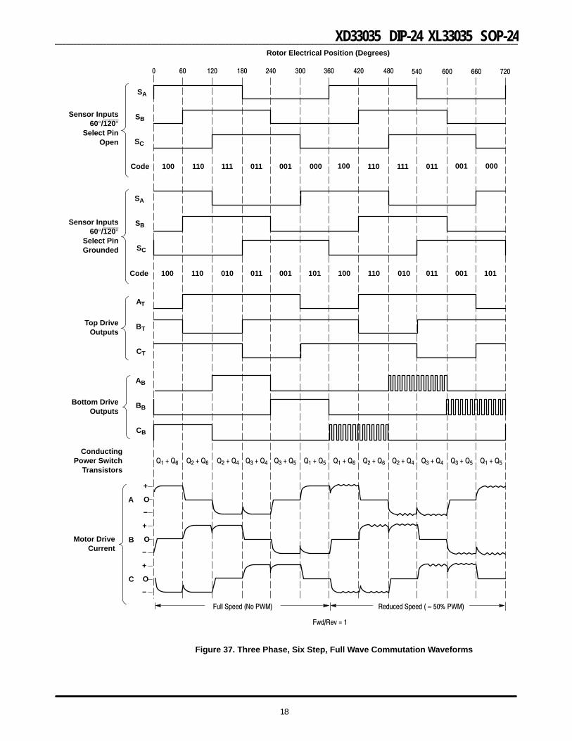
Figure 37. Three Phase, Six Step, Full Wave Commutation Waveforms
Rotor Electrical Position (Degrees)
100 000001011111110100000001011111110
720660600540480420360300240180120600
SA
SB
SC
Code
SC
SB
Code
SA
Sensor Inputs60°/120°
Select PinOpen
Sensor Inputs60°/120°
Select PinGrounded
AB
BB
Q2 + Q6
CB
Q2 + Q4 Q3 + Q4 Q3 + Q5 Q1 + Q5 Q1 + Q6
Bottom DriveOutputs
Q2 + Q6 Q2 + Q4 Q3 + Q4 Q3 + Q5
Motor DriveCurrent
B
Fwd/Rev = 1
C
−
O
+
−
O
+
ConductingPower Switch
TransistorsQ1 + Q5
Top DriveOutputs
Q1 + Q6
A
BT
AT
CT
−
O
+
100 110 001011 001011110100010 010 101101
Reduced Speed ( ≈ 50% PWM)Full Speed (No PWM)
18
XD33035 DIP-24 XL33035 SOP-24

Figure 38 shows a three phase, three step, half wave motorcontroller. This configuration is ideally suited forautomotive and other low voltage applications since there isonly one power switch voltage drop in series with a givenstator winding. Current flow is unidirectional or half wavebecause only one end of each winding is switched.Continuous braking with the typical half wave arrangementpresents a motor overheating problem since stator current islimited only by the winding resistance. This is due to the lackof upper power switch transistors, as in the full wave circuit,used to disconnect the windings from the supply voltage
VM. A unique solution is to provide braking until the motorstops and then turn off the bottom drives. This can beaccomplished by using the Fault Output in conjunction withthe Output Enable as an over current timer. ComponentsRDLY and CDLY are selected to give the motor sufficient timeto stop before latching the Output Enable and the top driveAND gates low. When enabling the motor, the brake switchis closed and the PNP transistor (along with resistors R1 andRDLY) are used to reset the latch by discharging CDLY. Thestator flyback voltage is clamped by a single zener and threediodes.
Figure 38. Three Phase, Three Step, Half Wave Motor Controller
Motor
9
24
20
QS
CT
R
RT
Oscillator
Gnd
ILimit
Error Amp
PWM
ThermalShutdown
ReferenceRegulator
Lockout
UndervoltageVM
4
2
1
21
16
10
11
13
8
12
3
17
22
7
6
5
Fwd/Rev
QR
S
19
Faster
60°/120°
SS
VM
SpeedSet
RotorPositionDecoder
18
Brake
15
14
23
CDLY
RDLY
R2
R1
25 μA
N
N
19
XD33035 DIP-24 XL33035 SOP-24

Three Phase Closed Loop ControllerThe 33035, by itself, is only capable of open loop
motor speed control. For closed loop motor speed control,the 33035 requires an input voltage proportional to themotor speed. Traditionally, this has been accomplished bymeans of a tachometer to generate the motor speed feedbackvoltage. Figure 39 shows an application whereby an33039, powered from the 6.25 V reference (Pin 8) of the33035, is used to generate the required feedback voltagewithout the need of a costly tachometer. The same Hallsensor signals used by the 33035 for rotor positiondecoding are utilized by the 33039. Every positive ornegative going transition of the Hall sensor signals on anyof the sensor lines causes the 33039 to produce an outputpulse of defined amplitude and time duration, as determinedby the external resistor R1 and capacitor C1. The output train
Figure 39. Closed Loop Brushless DC Motor ControlUsing The 33035 and 33039
Motor
TP2
0.05/1.0 W
0.1 33
TP1
1.0 k
VM (18 to 30 V)
10000.11.1 k
Close Loop
0.1
1.0 M
0.01Speed
Faster
4.7 k
F/RBrake
1.0 k
470
470
470
1N5819
1.1 k1.1 k
1.0 k
1
2
3
4
8
7
6
5
1
2
3
4
9
5
6
7
8
10
24
23
22
21
20
19
18
17
16
15
33035
33039
1.0 MR1
750 pFC1
10 k
S S
J2
100 k
10011
12
14
13
5.1 kEnable J1
330
47 μF
1N5355B18 V
2.2 k
0.1
1N4148
Latch OnFault
Fault
Reset
N
N
2.2 k
20
XD33035 DIP-24 XL33035 SOP-24
(J2) at Pin 22 of the 33035.Hall sensor electrical phasing by removing the jumper can easily be modified to accommodate 60/300 degree 120/240 degrees Hall sensor electrical phasing. The system system shown in Figure 39 is designed for a motor having breaking, and change of direction of the motor. The High currents can be expected during conditions of start−up, outputs drive a TMOS power MOSFET 3−phase bridge. controller and closes the feedback loop. The 33035 PWM reference level at Pin 13 of the 33035 motor motor speed. This speed proportional voltage establishes the produce a DC voltage level which is proportional to the amplifier of the 33035 configured as an integrator to of pulses at Pin 5 of the 33039 are integrated by the error

Sensor Phasing ComparisonThere are four conventions used to establish the relative
phasing of the sensor signals in three phase motors. With sixstep drive, an input signal change must occur every 60electrical degrees; however, the relative signal phasing isdependent upon the mechanical sensor placement. Acomparison of the conventions in electrical degrees is shownin Figure 40. From the sensor phasing table in Figure 41,note that the order of input codes for 60° phasing is thereverse of 300°. This means the 33035, when configuredfor 60° sensor electrical phasing, will operate a motor witheither 60° or 300° sensor electrical phasing, but resulting inopposite directions of rotation. The same is true for the partwhen it is configured for 120° sensor electrical phasing; themotor will operate equally, but will result in oppositedirections of rotation for 120° for 240° conventions.
Figure 40. Sensor Phasing Comparison
Rotor Electrical Position (Degrees)
300°
240°
720660600540480420360300240180120600
SB
SA
120°
60°
SC
SA
SB
SC
SC
SB
SA
SC
SB
SA
Sen
sor
Ele
ctri
cal P
has
ing
Sensor Electrical Phasing (Degrees)
60° 120° 240° 300°
SA SB SC SA SB SC SA SB SC SA SB SC
1 0 0 1 0 1 1 1 0 1 1 1
1 1 0 1 0 0 1 0 0 1 1 0
1 1 1 1 1 0 1 0 1 1 0 0
0 1 1 0 1 0 0 0 1 0 0 0
0 0 1 0 1 1 0 1 1 0 0 1
0 0 0 0 0 1 0 1 0 0 1 1
Figure 41. Sensor Phasing Table
In this data sheet, the rotor position is always given inelectrical degrees since the mechanical position is a functionof the number of rotating magnetic poles. The relationshipbetween the electrical and mechanical position is:
Electrical Degrees � Mechanical Degrees�#Rotor Poles2
�An increase in the number of magnetic poles causes more
electrical revolutions for a given mechanical revolution.General purpose three phase motors typically contain a fourpole rotor which yields two electrical revolutions for onemechanical.
Two and Four Phase Motor CommutationThe 33035 is also capable of providing a four step
output that can be used to drive two or four phase motors.The truth table in Figure 42 shows that by connecting sensorinputs SB and SC together, it is possible to truncate thenumber of drive output states from six to four. The outputpower switches are connected to BT, CT, BB, and CB.Figure 43 shows a four phase, four step, full wave motorcontrol application. Power switch transistors Q1 through Q8are Darlington type, each with an internal parasitic catchdiode. With four step drive, only two rotor position sensorsspaced at 90 electrical degrees are required. Thecommutation waveforms are shown in Figure 44.
Figure 45 shows a four phase, four step, half wave motorcontroller. It has the same features as the circuit in Figure 38,except for the deletion of speed control and braking.
Inputs Outputs
Sensor ElectricalSpacing* = 90°
Top Drives Bottom Drives
SA SB F/R BT CT BB CB
1100
0110
1111
1011
1101
0001
1000
1100
0110
0000
1110
0111
0100
0010
21
XD33035 DIP-24 XL33035 SOP-24
Commutation Truth TableFigure 42. Two and Four Phase, Four Step,
*With 33035 sensor input SB connected to SC.
33035 (60°/120° Select Pin Open)

CT
RT
VM
Enab
le
Fwd/
Rev
101312118177223654
91920
Lock
out
21
Rot
or
Und
ervo
ltage
241
Mo
tor
2
Ref
eren
ce
Ther
mal
Osc
illato
r
Gnd
16
Q5Q1
Q2
Q6
Q7
Q3
Q4
Q8
V M
R
CR
S
Posi
tion
Dec
oder
Shut
dow
n
Reg
ulat
or
Erro
r Am
p
PWM
I Lim
it
SRQ
RSQ
A B DC
S
S
18
1514
23
25
Aμ
Faul
tIn
d.
N
N
Figure 43. Four Phase, Four Step, Full Wave Motor Controller
22
XD33035 DIP-24 XL33035 SOP-24

ConductingPower Switch
Transistors
A
SA
SB
Code
Q3 + Q5
Rotor Electrical Position (Degrees)
Fwd/Rev = 1
-
O
+
−
−
D
C
+
O
−
O
+
B
+
CB
O
BB
CT
BT
Q2 + Q8Q1 + Q7Q4 + Q6Q3 + Q5Q2 + Q8Q1 + Q7Q4 + Q6
0001111000011010
Motor DriveCurrent
Bottom DriveOutputs
Top DriveOutputs
Sensor Inputs60°/120°
Select PinOpen
180 270 360 450 540 630 7200 90
Figure 44. Four Phase, Four Step, Full Wave Motor Controller
Full Speed (No PWM)
23
XD33035 DIP-24 XL33035 SOP-24

R
VM
RS
Mo
tor
SN
CT
RT
VM
Enab
le
Fwd/
Rev
101312118177223654
91920
Lock
out
21
Rot
or
Und
ervo
ltage
2412
Ref
eren
ce
Ther
mal
Osc
illato
r
Gnd
16
Posi
tion
Dec
oder
Shut
dow
n
Reg
ulat
or
Erro
r Am
p
PWM
I Lim
it
SRQ
RSQ
18
1514
23 Brak
e
25
Aμ
Faul
tIn
d.
C
NS
Figure 45. Four Phase, Four Step, Half Wave Motor Controller
24
XD33035 DIP-24 XL33035 SOP-24

Brush Motor ControlThough the 33035 was designed to control brushless
DC motors, it may also be used to control DC brush typemotors. Figure 46 shows an application of the 33035driving a MOSFET H−bridge affording minimal parts countto operate a brush−type motor. Key to the operation is theinput sensor code [100] which produces a top−left (Q1) anda bottom−right (Q3) drive when the controller’sforward/reverse pin is at logic [1]; top−right (Q4), bottom−left(Q2) drive is realized when the Forward/Reverse pin is atlogic [0]. This code supports the requirements necessary forH−bridge drive accomplishing both direction and speedcontrol.
The controller functions in a normal manner with a pulsewidth modulated frequency of approximately 25 kHz.Motor speed is controlled by adjusting the voltage presentedto the noninverting input of the error amplifier establishingthe PWM’s slice or reference level. Cycle−by−cycle currentlimiting of the motor current is accomplished by sensing thevoltage (100 mV) across the RS resistor to ground of theH−bridge motor current. The over current sense circuit
makes it possible to reverse the direction of the motor, usingthe normal forward/reverse switch, on the fly and not haveto completely stop before reversing.
LAYOUT CONSIDERATIONS
Do not attempt to construct any of the brushless motorcontrol circuits on wire−wrap or plug−in prototypeboards. High frequency printed circuit layout techniquesare imperative to prevent pulse jitter. This is usually causedby excessive noise pick−up imposed on the current sense orerror amp inputs. The printed circuit layout should containa ground plane with low current signal and high drive andoutput buffer grounds returning on separate paths back to thepower supply input filter capacitor VM. Ceramic bypasscapacitors (0.1 μF) connected close to the integrated circuitat VCC, VC, Vref and the error amp noninverting input maybe required depending upon circuit layout. This provides alow impedance path for filtering any high frequency noise.All high current loops should be kept as short as possibleusing heavy copper runs to minimize radiated EMI.
25
XD33035 DIP-24 XL33035 SOP-24

9
24
20
QS
0.005
R
10 k
Oscillator
Gnd
ILimit
Error Amp
PWM
ThermalShutdown
ReferenceRegulator
Lockout
Undervoltage+12 V
4
2
1
21
16
10
11
13
8
12
3
17
22
7
6
5
Fwd/Rev
QR
S
19
Faster
RotorPositionDecoder
18
Brake
15
14
23
25 μA
Figure 46. H−Bridge Brush−Type Controller
RS
1.0 k
0.001
22
22
DC BrushMotor
M
+12 V
1.0 k
1.0 k
Q1*
Q2*
Q4*
Q3*
Enable
10 k
FaultInd.
20 k
26
XD33035 DIP-24 XL33035 SOP-24

26 27
XD33035 DIP-24 XL33035 SOP-24