4.5V TO 18V INPUT 10 PIN SYNCHRONOUS BUCK CONTROLLER ...
40
1FEATURES CONTENTS DESCRIPTION APPLICATIONS 1 2 3 4 10 9 8 7 HDRV SW BOOT LDRV ENABLE FB COMP VDD TPS40192/3 5 6 BP5 PGD 11 GND UDG-06063 V OUT ON/OFF External Logic Supply 5V or Less, or BP5 V IN V OUT TPS40192, TPS40193 SLUS719B–MARCH 2007–REVISED SEPTEMBER 2007 www.ti.com 4.5-V TO 18-V INPUT 10-PIN SYNCHRONOUS BUCK CONTROLLER WITH POWER GOOD • Input Operating Voltage Range: 4.5 V to 18 V Device Ratings 3 • Up to 20-A Output Currents Electrical Characteristics 4 • Supports Pre-Biased Outputs Typical Characteristics 6 • 0.5% 0.591-V Reference • 600 kHz (TPS40192) and 300 kHz (TPS40193) Terminal Information 9 Switching Frequencies Application Information 11 • Three Selectable Thermally Compensated Design Example 17 Short Circuit Protection Levels Additional References 27 • Hiccup Restart from Faults • Internal 5-V Regulator • High and Low side FET RDS ON Current Sensing TPS40192 and TPS40193 are cost-optimized synchronous buck controllers that operate from 4.5 V • 10-Pin 3 mm × 3 mm SON Package to 18 V input. These controllers implement a • Internal 4-ms Soft-Start Time voltage-mode control architecture with the switching • Thermal Shutdown Protection at 145°C frequency fixed at either 600 kHz (TPS40192) or 300 kHz (TPS40193). The higher switching frequency facilitates the use of smaller inductor and output capacitors, thereby providing a compact • Cable Modem CPE power-supply solution. An adaptive anti-cross • Digital Set Top Box conduction scheme is used to prevent shoot through • Graphics/Audio Cards current in the power FETs. • Entry Level and Mid-Range Servers SIMPLIFIED APPLICATION DIAGRAM 1 Please be aware that an important notice concerning availability, standard warranty, and use in critical applications of Texas Instruments semiconductor products and disclaimers thereto appears at the end of this data sheet. PRODUCTION DATA information is current as of publication date. Copyright © 2007, Texas Instruments Incorporated Products conform to specifications per the terms of the Texas Instruments standard warranty. Production processing does not necessarily include testing of all parameters.
-
Upload
khangminh22 -
Category
Documents
-
view
2 -
download
0
Transcript of 4.5V TO 18V INPUT 10 PIN SYNCHRONOUS BUCK CONTROLLER ...

1FEATURES CONTENTS
DESCRIPTION
APPLICATIONS
1
2
3
4
10
9
8
7
HDRV
SW
BOOT
LDRV
ENABLE
FB
COMP
VDD
TPS40192/3
5 6BP5PGD
11
GND
UDG−06063
VOUT
ON/OFF External LogicSupply
5V or Less,or BP5
VIN
VOUT
TPS40192, TPS40193
SLUS719B–MARCH 2007–REVISED SEPTEMBER 2007www.ti.com
4.5-V TO 18-V INPUT 10-PIN SYNCHRONOUS BUCK CONTROLLER WITH POWER GOOD
• Input Operating Voltage Range: 4.5 V to 18 VDevice Ratings 3• Up to 20-A Output CurrentsElectrical Characteristics 4• Supports Pre-Biased OutputsTypical Characteristics 6• 0.5% 0.591-V Reference
• 600 kHz (TPS40192) and 300 kHz (TPS40193) Terminal Information 9Switching Frequencies Application Information 11
• Three Selectable Thermally CompensatedDesign Example 17Short Circuit Protection LevelsAdditional References 27• Hiccup Restart from Faults
• Internal 5-V Regulator• High and Low side FET RDSON Current
Sensing TPS40192 and TPS40193 are cost-optimizedsynchronous buck controllers that operate from 4.5 V• 10-Pin 3 mm × 3 mm SON Packageto 18 V input. These controllers implement a• Internal 4-ms Soft-Start Time voltage-mode control architecture with the switching
• Thermal Shutdown Protection at 145°C frequency fixed at either 600 kHz (TPS40192) or 300kHz (TPS40193). The higher switching frequencyfacilitates the use of smaller inductor and outputcapacitors, thereby providing a compact• Cable Modem CPEpower-supply solution. An adaptive anti-cross• Digital Set Top Box conduction scheme is used to prevent shoot through
• Graphics/Audio Cards current in the power FETs.• Entry Level and Mid-Range Servers
SIMPLIFIED APPLICATION DIAGRAM
1
Please be aware that an important notice concerning availability, standard warranty, and use in critical applications ofTexas Instruments semiconductor products and disclaimers thereto appears at the end of this data sheet.
PRODUCTION DATA information is current as of publication date. Copyright © 2007, Texas Instruments IncorporatedProducts conform to specifications per the terms of the TexasInstruments standard warranty. Production processing does notnecessarily include testing of all parameters.

www.ti.com
DESCRIPTION (continued)
TPS40192, TPS40193
SLUS719B–MARCH 2007–REVISED SEPTEMBER 2007
Short circuit detection is done by sensing the voltage drop across the low-side MOSFET when it is on andcomparing it with a user selected threshold of 100 mV, 200 mV or 280 mV. The threshold is set with a singleexternal resistor connected from COMP to GND. This resistor is sensed at startup and the selected threshold islatched. Pulse by pulse limiting (to prevent current runaway) is provided by sensing the voltage across thehigh-side MOSFET when it is on and terminating the cycle when the voltage drop rises above a fixed threshold of550 mV. When the controller senses an output short circuit, both MOSFETs are turned off and a timeout periodis observed before attempting to restart. This provides limited power dissipation in the event of a sustained fault.
ORDERING INFORMATIONTAPE AND REELTJ PACKAGE FREQUENCY (kHz) PART NUMBERQUANTITY
250 TPS40193DRCT300
3000 TPS40193DRCR-40°C to 85°C Plastic 10-Pin SON (DRC)
250 TPS40192DRCT600
3000 TPS40192DRCR
2 Submit Documentation Feedback Copyright © 2007, Texas Instruments Incorporated
Product Folder Link(s): TPS40192 TPS40193

www.ti.com
DEVICE RATINGS
ABSOLUTE MAXIMUM RATINGS
RECOMMENDED OPERATING CONDITIONS
PACKAGE DISSIPATION RATINGS
ELECTROSTATIC DISCHARGE (ESD) PROTECTION
TPS40192, TPS40193
SLUS719B–MARCH 2007–REVISED SEPTEMBER 2007
over operating free-air temperature range unless otherwise noted (1)
TPS40192/TPS40193 UNITVDD, ENABLE –0.3 to 20SW –5 to 25
Input voltage range BOOT, HDRV –0.3 to 30 VBOOT-SW, HDRV-SW (differential from BOOT or HDRV to SW) -0.3 to 6COMP, FB, BP5, LDRV, PGD –0.3 to 6
TJ Operating junction temperature range –40 to 150°C
Tstg Storage temperature –55 to 150
(1) Stresses beyond those listed under "absolute maximum ratings" may cause permanent damage to the device. These are stress ratingsonly, and functional operation of the device at these or any other conditions beyond those indicated under "recommended operatingconditions" is not implied. Exposure to absolute-maximum-rated conditions for extended periods may affect device reliability.
MIN NOM MAX UNITVVDD Input voltage 4.5 18 VTJ Operating Junction temperature -40 125 °C
RθJA High-K Board (1) Power Rating (W) Power Rating (W)PACKAGE AIRFLOW (LFM) (°C/W) TA = 25°C TA = 85°C0 (Natural Convection) 47.9 2.08 0.835
DRC 200 40.5 2.46 0.987400 38.2 2.61 1.04
(1) Ratings based on JEDEC High Thermal Conductivity (High K) Board. For more information on the test method, see TI Technical BriefSZZA017.
MIN TYP MAX UNITHuman Body Model (HBM) 2500
VCharged Device Model (CDM) 1500
Copyright © 2007, Texas Instruments Incorporated Submit Documentation Feedback 3
Product Folder Link(s): TPS40192 TPS40193

www.ti.com
ELECTRICAL CHARACTERISTICS
TPS40192, TPS40193
SLUS719B–MARCH 2007–REVISED SEPTEMBER 2007
TJ = –40°C to 85°C, VVDD= 12 Vdc, all parameters at zero power dissipation (unless otherwise noted)
PARAMETER TEST CONDITIONS MIN TYP MAX UNITREFERENCE
0°C ≤ TJ ≤ 85°C 588 591 594VFB Feedback voltage range mV
-40°C ≤ TJ ≤ 85°C 585 591 594INPUT SUPPLYVVDD Input voltage range 4.5 18.0 V
VENABLE = 3 V 2.5 4.0 mAIVDD Operating current
VENABLE = 0.6 V 45 70 μAON BOARD REGULATORV5VBP Output voltage VVDD > 6 V, I5VBP ≤ 10 mA 5.1 5.3 5.5 VVDO Regulator dropout voltage VVDD - VBP5 , VVDD = 5 V, IBP5 ≤ 25 mA 350 550 mVISC Regulator current limit threshold 50
mAIBP5 Average current 50OSCILLATOR
TPS40193 240 300 360fSW Switching frequency kHz
TPS40192 500 600 700VRMP Ramp amplitude (1) 1 VPWMDMAX Maximum duty cycle (1) 85%tON(min) Minimum controlled pulse (1) 110
HDRV off to LDRV on 50 nstDEAD Output driver dead time
LDRV off to HDRV on 25SOFT-STARTtSS Soft-start time 3 4 6tSSDLY Soft-start delay time 2 mstREG Time to regulation 6ERROR AMPLIFIERGBWP Gain bandwidth product (1) 7 10 MHzAOL DC gain (1) 60 dB
Input bias current (current out of FBIIB 100 nApin)IEAOP Output source current VFB = 0 V 1
mAIEAOM Output sink current VFB = 2 V 1SHORT CIRCUIT PROTECTIONtPSS(min) Minimum pulse during short circuit (1) 250
nstBLNK Blanking time (1) 60 90 120tOFF Off-time between restart attempts 30 50 ms
RCOMP(GND) = OPEN, TJ = 25°C 160 200 240Short circuit comparator thresholdVILIM RCOMP(GND) = 4 kΩ, TJ = 25°C 80 100 120voltage
mVRCOMP(GND) = 12 kΩ, TJ = 25°C 228 280 342Short circuit threshold voltage onVILIMH TJ = 25°C 400 550 650high-side MOSFET
(1) Ensured by design. Not production tested.
4 Submit Documentation Feedback Copyright © 2007, Texas Instruments Incorporated
Product Folder Link(s): TPS40192 TPS40193

www.ti.com
TPS40192, TPS40193
SLUS719B–MARCH 2007–REVISED SEPTEMBER 2007
ELECTRICAL CHARACTERISTICS (continued)TJ = –40°C to 85°C, VVDD= 12 Vdc, all parameters at zero power dissipation (unless otherwise noted)
PARAMETER TEST CONDITIONS MIN TYP MAX UNITOUTPUT DRIVERSRHDHI High-side driver pull-up resistance VBOOT - VSW = 4.5 V, IHDRV = -100 mA 3 6RHDLO High-side driver pull-down resistance VBOOT - VSW = 4.5 V, IHDRV = 100 mA 1.5 3.0
ΩRLDHI Low-side driver pull-up resistance ILDRV = -100 mA 2.5 5.0RLDLO Low-side driver pull-down resistance ILDRV = 100 mA 0.8 1.5tHRISE High-side driver rise time (2) 15 35tHFALL High-side driver fall time (2) 10 25
CLOAD = 1 nF nstLRISE Low-side driver rise time (2) 15 35tLFALL Low-side driver fall time (2) 10 25UVLOVUVLO Turn-on voltage 3.9 4.2 4.4 VUVLOHYST Hysteresis 700 800 900 mVSHUTDOWNVIH High-level input voltage, ENABLE 1.9 3.0
VVIL Low-level input votlage, ENABLE 0.6POWER GOODVOV Feedback voltage limit for powergood 650VUV Feedback voltage limit for powergood 525 mVVPG_HYST Powergood hysteresis voltage at FB pin 30RPGD Pulldown resistance of PGD pin VFB = 0 V 7 50 ΩIPDGLK Leakage current VFB = 0 V 7 12 μABOOT DIODEVDFWD Bootstrap diode forward voltage IBOOT = 5 mA 0.5 0.8 1.2 VTHERMAL SHUTDOWNTJSD Junction shutdown temperature (2) 145
°CTJSDH Hysteresis (2) 20
(2) Ensured by design. Not production tested.
Copyright © 2007, Texas Instruments Incorporated Submit Documentation Feedback 5
Product Folder Link(s): TPS40192 TPS40193

www.ti.com
TYPICAL CHARACTERISTICS
TJ − Junction T emperature − °C
VFB
− R
elat
ive
Rev
eref
nce
Vol
tage
Cha
nge
− %
−40 −25 −10 5 20 35 95 12550 65 80 110−0.50
−0.45
−0.40
−0.20
−0.15
−0.05
−0.35
−0.30
−0.25
0.00
0.50
−0.10
−40 −25 −10 5 20 35 95 125−4.5
−4.0
−3.5
−1.5
−1.0
−0.5
0.5
−3.0
−2.5
−2.0
0.0
50 65 80 110
f SW
− R
elat
ive
Osc
illat
or F
requ
ency
Cha
nge
− %
TJ − Junction T emperature − °C
I VD
D −
Shu
tdow
n C
urre
nt −
µA
TJ − Junction T emperature − °C
0
10
20
30
40
50
60
−40 −25 −10 5 20 35 9550 65 80 110 125
VENABLE < 0.6 V
VE
NA
BLE
− E
nabl
e T
hres
hold
Vol
tage
− V
TJ − Junction T emperature − °C
0
0.5
1.0
1.5
2.0
2.5
−40 −25 −10 5 20 35 95 12550 65 80 110
Turn On
Turn Off
TPS40192, TPS40193
SLUS719B–MARCH 2007–REVISED SEPTEMBER 2007
RELATIVE REFERENCE FEEDBACK VOLTAGE RELATIVE OSCILLATOR FREQUENCY CHANGEvs vs
JUNCTION TEMPERATURE JUNCTION TEMPERATURE
Figure 1. Figure 2.
SHUTDOWN INPUT CURRENT ENABLE THRESHOLD VOLTAGEvs vs
JUNCTION TEMPERATURE JUNCTION TEMPERATURE
Figure 3. Figure 4.
6 Submit Documentation Feedback Copyright © 2007, Texas Instruments Incorporated
Product Folder Link(s): TPS40192 TPS40193

www.ti.com
t SS −
Sof
t sta
rt T
ime
− m
s
TJ − Junction T emperature − °C
3.75
3.80
3.85
3.90
3.95
4.00
4.05
−40 −25 −10 5 20 35 95 12550 65 80 110 −40 −25 −10 5 20 35 95 12550 65 80 1100
50
150
200
250
350
400
100
300
VIL
IM −
Cur
rent
Lim
it T
hres
hold
− m
V
TJ − Junction T emperature − °C
RCOMP = 4 kΩ
RCOMP = OPEN
RCOMP = 12 kΩ
0
100
300
400
600
700
800
500
200
−40 −25 −10 5 20 35 95 12550 65 80 110
VIL
IMH
− C
urre
nt L
imit
Thr
esho
ld −
mV
TJ − Junction T emperature − °C
t RE
G −
Reg
ulat
ion
Tim
e −
ms
TJ − Junction T emperature − °C
4.4
5.3
5.7
6.1
6.3
5.5
4.7
−40 −25 −10 5 20 35 95 12550 65 80 110
4.9
5.1
5.5
5.9
TPS40192, TPS40193
SLUS719B–MARCH 2007–REVISED SEPTEMBER 2007
TYPICAL CHARACTERISTICS (continued)
SOFT START TIME LOW-SIDE MOSFET CURRENT LIMIT THRESHOLDvs vs
JUNCTION TEMPERATURE JUNCTION TEMPERATURE
Figure 5. Figure 6.
HIGH-SIDE MOSFET CURRENT LIMIT THRESHOLD TOTAL TIME TO REGULATIONvs vs
JUNCTION TEMPERATURE JUNCTION TEMPERATURE
Figure 7. Figure 8.
Copyright © 2007, Texas Instruments Incorporated Submit Documentation Feedback 7
Product Folder Link(s): TPS40192 TPS40193

www.ti.com
4 6 8 10 12 14 16 180
10
40
70
80
100
60
30
20
90
50
I VD
D −
Sup
ply
Cur
rent
−
µA
VVDD − Input V oltage − V
VENABLE < 0.6 V
VO
V, V
UV −
Pow
ergo
od T
hres
hold
Vol
tage
− m
V
TJ − Junction T emperature − °C
560
580
540
520
500
660
680
640
620
600
−40 −25 −10 5 20 35 95 12550 65 80 110
Overvoltage
Undervoltage
0.4 0.6 0.8 1.0 1.2 1.4 1.60
0.5
3.0
3.5
4.5
1.5
1.0
5.0
2.0
2.5
4.0
1-D - Freewheel Time - ms
I OC
-R
ela
tive
Overc
urr
en
tT
rip
Po
int
-A
TPS40192, TPS40193
SLUS719B–MARCH 2007–REVISED SEPTEMBER 2007
TYPICAL CHARACTERISTICS (continued)
POWERGOOD THRESHOLD VOLTAGE SHUTDOWN CURRENTvs vs
JUNCTION TEMPERATURE INPUT VOLTAGE
Figure 9. Figure 10.
RELATIVE OVERCURRENT TRIP POINTvs
FREEWHEEL TIME
Figure 11.
8 Submit Documentation Feedback Copyright © 2007, Texas Instruments Incorporated
Product Folder Link(s): TPS40192 TPS40193

www.ti.com
DEVICE INFORMATION
DRC PACKAGE(TOP VIEW)
PGD
5
VDD
4
COMP
3
FB
2
ENABLE
1
6 7 8 9 10
BP5 LDRV BOOT SW HDRV
TPS40192TPS40193
TPS40192, TPS40193
SLUS719B–MARCH 2007–REVISED SEPTEMBER 2007
Table 1. TERMINAL FUNCTIONSTERMINAL
I/O DESCRIPTIONNAME NO.
Gate drive voltage for the high-side N-channel MOSFET. A capacitor 100 nF typical must be connectedBOOT 8 I between this pin and SW.Output bypass for the internal regulator. Connect at least 1μF capacitor from this pin to GND. Largercapacitors, up to 4.7μF will improve noise performance when using a low side FET with a gate charge of
BP5 6 O 25nC or greater. Low power, low noise loads may be connected here if desired. The sum of the externalload and the gate drive requirements must not exceed 50 mA. This regulator is turned off when ENABLE ispulled low.
COMP 3 O Output of the error amplifier.Logic level input which starts or stops the controller from an external user command. A high-level turns the
ENABLE 1 I controller on. A weak internal pull-up holds this pin high so that the pin may be left floating if this function isnot used.Inverting input to the error amplifier. In normal operation the voltage on this pin is equal to the internalFB 2 I reference voltage (591 mV typical)
GND (11) - Thermal pad ground connection. Common reference for the device. Connect to the system GND.HDRV 10 O Bootstrapped output for driving the gate of the high side N channel FET.LDRV 7 O Output to the rectifier MOSFET gatePGD 5 O Open drain power good output
Sense line for the adaptive anti-cross conduction circuitry. Serves as common connection for the flying highSW 9 I side MOSFET driverVDD 4 I Power input to the controller
Copyright © 2007, Texas Instruments Incorporated Submit Documentation Feedback 9
Product Folder Link(s): TPS40192 TPS40193

www.ti.com
ENABLE 1
VDD 4
BP5 6
COMP 3
FB 2
GND PP
5 V
Regulator 4.2 V +
5 V
UVLO
+
Error
Amplifier
591 mV
SS
+
Fault
Controller
Soft Start
Ramp
Generator
PWM Logic
and
Anti-Cross
Conduction
+
VDD - 0.5 V
Oscillator
Short Circuit
Threshold
Selector
SD
UVLO
UVLO
SS
SD
FAULT
UVLO
+
CLK
10CLK
8
7
9
5
ENABLE
HDRV
SW
LDRV
PGD
5 V
Powergood
Control
FB
SD
FAULT
5 V
SC Threshold Latch
SC: -110 mV, -200 mV, or -280 mV
750 kW
VDD
SC
SD
+
FAULTOCL
OCH
UDG-06064
TPS40192, TPS40193
SLUS719B–MARCH 2007–REVISED SEPTEMBER 2007
10 Submit Documentation Feedback Copyright © 2007, Texas Instruments Incorporated
Product Folder Link(s): TPS40192 TPS40193
www.ti.com
APPLICATION INFORMATION
Introduction
Voltage Reference
Oscillator
UVLO
TPS40192, TPS40193
SLUS719B–MARCH 2007–REVISED SEPTEMBER 2007
The TPS40192 and TPS40193 are cost optimized controllers providing all the necessary features to construct ahigh performance DC/DC converter while keeping costs to a minimum. Support for pre-biased outputs eliminatesconcerns about damaging sensitive loads during startup. Strong gate drivers for the high side and rectifierN-channel MOSFETs decrease switching losses for increased efficiency. Adaptive gate drive timing preventsshoot through and minimizes body diode conduction in the rectifier MOSFET, also increasing efficiency.Selectable short circuit protection thresholds and hiccup recovery from a short circuit increase design flexibilityand minimize power dissipation in the event of a prolonged output fault. A dedicated enable pin (ENABLE) allowsthe converter to be placed in a very low quiescent current shutdown mode. Internally fixed switching frequencyand soft-start time reduce external component count, simplifying design and layout, as well as reducing footprintand cost. The 3 mm × 3 mm package size also contributes to a reduced overall converter footprint.
The band gap cell is designed with a trimmed 591 mV output. The 0.5% tolerance on the reference voltageallows the user to design a very accurate power-supply.
The TPS40192 has a fixed internal switching frequency of 600 kHz while the TPS40193 operates at 300 kHz.
When the input voltage is below the UVLO threshold, the device holds all gate drive outputs in the low (OFF)state. When the input rises above the UVLO threshold, and the ENABLE pin is above the turn ON threshold, theoscillator begins to operate and the start-up sequence is allowed to begin. The UVLO level is internally fixed at4.2 V.
Copyright © 2007, Texas Instruments Incorporated Submit Documentation Feedback 11
Product Folder Link(s): TPS40192 TPS40193

www.ti.com
Enable Functionality
4
1
5
ToEnableChip
VDD
ENABLE
GND
1.5 MΩ
200 kΩ
1 kΩ
1 kΩ
300 kΩ
200 Ω
UDG−05061
TPS40192, TPS40193
SLUS719B–MARCH 2007–REVISED SEPTEMBER 2007
The TPS40192 and TPS40193 have a dedicated ENABLE pin. This simplifies user level interface design sinceno multiplexed functions exist. Another benefit is a true low power shutdown mode of operation. When theENABLE pin is pulled to GND, all unnecessary functions, including the BP5 regulator, are turned off, reducing thedevice IDD current to 45-uA. A functionally equivalent circuit of the enable circuitry shown in Figure 12.
Figure 12. TPS40192 ENABLE Pin Internal Circuitry
If the ENABLE pin is left floating, the chip starts automatically. The pin must be pulled to less than 600 mV toguarantee that the TPS40192/3 is in shutdown mode. Note that the ENABLE pin is relatively high impedance. Insome situations, there could be enough noise nearby to cause the ENABLE pin to swing below the 600 mVthreshold and give erroneous shutdown commands to the rest of the device. There are two solutions to thisproblem should it arise.1. Place a capacitor from ENABLE to GND. A side effect of this is to delay the start of the converter while the
capacitor charges past the enable threshold2. Place a resistor from VDD to ENABLE. This causes more current to flow in the shutdown mode, but does not
delay converter startup. If a resistor is used, the total current into the ENABLE pin should be limited to nomore than 500 μA.
12 Submit Documentation Feedback Copyright © 2007, Texas Instruments Incorporated
Product Folder Link(s): TPS40192 TPS40193

www.ti.com
Startup Sequence and Timing
ENABLE
COMP
VOUT
SC ThresholdConfigured
(1 ms)
Soft Start Time (4 ms)
CompensationNetwork Zeroed
(1 ms) UDG−06062
TPS40192, TPS40193
SLUS719B–MARCH 2007–REVISED SEPTEMBER 2007
The TPS40192/3 startup sequence is as follows. After input power is applied, the 5-V onboard regulator comesup. Once this regulator comes up, the device goes through a period where it samples the impedance at theCOMP pin and determines the short circuit protection threshold voltage, by placing 400 mV on the COMP pin forapproximately 1 ms. During this time, the current is measured and compared against internal thresholds to selectthe short circuit protection threshold. After this, the COMP pin is brought low for 1 ms. This ensures that thefeedback loop is preconditioned at startup and no sudden output rise occurs at the output of the converter whenthe converter is allowed to start switching. After these initial two milliseconds, the internal soft-start circuitry isengaged and the converter is allowed to start. See Figure 13.
Figure 13. Startup Sequence
Copyright © 2007, Texas Instruments Incorporated Submit Documentation Feedback 13
Product Folder Link(s): TPS40192 TPS40193

www.ti.com
Selecting the Short Circuit Current
0.4 VR1
et
R1C1 10 A
(1)
2
C1 R1
C2
3
COMP
TPS40192/3
FB
UDG−06061
VOUT RCOMP
TPS40192, TPS40193
SLUS719B–MARCH 2007–REVISED SEPTEMBER 2007
A short circuit in the TPS40192/3 is detected by sensing the voltage drop across the low-side FET when it is on,and across the high-side FET when it is on. If the voltage drop across either FET exceeds the short circuitthreshold in any given switching cycle, a counter increments one count. If the voltage across the high-side FETwas higher that the short circuit threshold, that FET is turned off early. If the voltage drop across either FET doesnot exceed the short circuit threshold during a cycle, the counter is decremented for that cycle. If the counter fillsup (a count of 7) a fault condition is declared and the drivers turn off both MOSFETs. After a timeout ofapproximately 50 ms, the controller attempts to restart. If a short circuit is still present at the output, the currentquickly ramps up to the short circuit threshold and another fault condition is declared and the process of waitingfor the 50 ms an attempting to restart repeats. The low side threshold will increase as the low side on timedecreases due to blanking time and comparator response time. See Figure 11 for changes in the threshold asthe low side FET conduction time decreases.
The TPS40192/3 provides three selectable short circuit protection thresholds for the low side FET: 100 mV,200 mV and 280 mV. The particular threshold is selected by connecting a resistor from COMP to GND. Table 2shows the short circuit thresholds for corresponding resistors from COMP to GND. When designing thecompensation for the feedback loop, remember that a low impedance compensation network combined with along network time constant can cause the short circuit threshold setting to not be as expected. The time constantand impedance of the network connected from COMP to FB should be as in Equation 1 to guarantee nointeraction with the short circuit threshold setting.
where• t is 1 ms, the sampling time of the short circuit threshold setting circuit• R1 and C1 are the values of the components in Figure 14
Figure 14. Short Circuit Threshold Feedback Network
14 Submit Documentation Feedback Copyright © 2007, Texas Instruments Incorporated
Product Folder Link(s): TPS40192 TPS40193

www.ti.com
ISCP(max) VILIM(max)
RDS(on)min (2)
ISCP(min) VILIM(min)
RDS(on)max (3)
IOUT(max) VILIM(min)
RDS(on)max (4)
TPS40192, TPS40193
SLUS719B–MARCH 2007–REVISED SEPTEMBER 2007
Table 2. Short Circuit Threshold Voltage SelectionCOMPARATOR RESISTANCE CURRENT LIMIT THRESHOLD
RCOMP (kΩ) VOLTAGE (mV)VILIM(V)
12 ±10% 280Open 200
4 ±10% 100
The range of short circuit current thresholds that can be expected is shown in Equation 2 and Equation 3.
where• ISCP is the short circuit current• VILIM is the short circuit threshold for the low-side MOSFET• RDS(on) is the channel resistance of the low-side MOSFET
Note that due to blanking time considerations, overcurrent threshold accuracy may fall off for duty cycle greaterthan 75% with the TPS40192, or 88% with the TPS40193. The reason for this is that the over current comparatorwill have only a very short time to sample the SW pin voltage under these conditions and may not have time torespond to voltages very near the threshold.
The short circuit protection threshold for the high-side MOSFET is fixed at 550 mV typical, 400 mV minimum.This threshold is in place to provide a maximum current output using pulse by pulse current limit in the case of afault. The pulse will be terminated when the voltage drop acros the high side FET exceeds the short circuitthreshold. The maximum amount of current that can be guaranteed to be sourced from a converter can be foundby Equation 4.
where• IOUT(max) is the maximum current that the converter is guaranteed to source• VILIMH(min) is the short circuit threshold for the high-side MOSFET (400 mV)• RDS(on)max is the maximum resistance of the high-side MOSFET
If the required current from the converter is greater than the calculated IOUT(max) , a lower resistance high-sideMOSFET must be chosen. Both the high side and low side thresholds use temperature compensation toapproximate the change in resistance for a typical power MOSFET. This will help couneract shifts in overcurrentthresholds as temperature increases. For this to be effective, the MOSFETs and the IC must be well coupledthermally.
Copyright © 2007, Texas Instruments Incorporated Submit Documentation Feedback 15
Product Folder Link(s): TPS40192 TPS40193

www.ti.com
5-V Regulator
IG fSW QG (high) QG (low)
(5)
TPS40192, TPS40193
SLUS719B–MARCH 2007–REVISED SEPTEMBER 2007
These devices have an on board 5-V regulator that allows the parts to operate from a single voltage feed. Noseparate 5-V feed to the part is required. This regulator needs to have a minimum of 1-μF of capacitance on theBP5 pin to guarantee stability. A ceramic capacitor is suggested for this purpose.
This regulator can also be used to supply power to nearby circuitry, eliminating the need for a separate LDO insome cases. If this pin is used for external loads, be aware that this is the power supply for the internals of theTPS40192/3. While efforts have been made to reduce sensitivity, any noise induced on this line has an adverseeffect on the overall performance of the internal circuitry and shows up as increased pulse jitter, or skewedreference voltage. Also, when the device is disabled by pulling the EN pin low, this regulator is turned off and willnot be available to supply power.
The amount of power available from this pin varies with the size of the power MOSFETs that the drivers mustoperate. Larger MOSFETs require more gate drive current and reduce the amount of power available on this pinfor other tasks. The total current that can be drwan from this pin by both the gate drive and external loads cannotexceed 50mA. The IC itself will use up to 4mA from the regulator and the total gate drive current can be foundfrom Equation 5.
For regulator stability, a 1-μF capacitor is required to be connected from BP5 to GND. In some applications usinghigher gate charge MOSFETs, a larger capacitor is required for noise suppression. For a total gate charge ofboth the high and low side MOSFETs greater than 20 nC, a 2.2-μF or larger capacitor is recommended.
where• IG is the required gate drive current• fSW is the switching frequency (600 kHz for TPS40192, and 300 kHz for TPS40193)• QG(high) is the gate charge requirement for the high-side FET when VGS=5 V• QG(low) is the gate charge requirement for the low-side FET when VGS=5 V
16 Submit Documentation Feedback Copyright © 2007, Texas Instruments Incorporated
Product Folder Link(s): TPS40192 TPS40193

www.ti.com
Pre-Bias Startup
Drivers
Power Good
Thermal Shutdown
TPS40192, TPS40193
SLUS719B–MARCH 2007–REVISED SEPTEMBER 2007
The TPS40192/3 contains a unique circuit to prevent current from being pulled from the output during startup inthe condition the output is pre-biased. When the soft-start commands a voltage higher than the pre-bias level(internal soft-start becomes greater than feedback voltage [VFB]), the controller slowly activates synchronousrectification by starting the first LDRV pulses with a narrow on-time. It then increments that on-time on acycle-by-cycle basis until it coincides with the time dictated by (1-D), where D is the duty cycle of the converter.This scheme prevents the initial sinking of the pre-bias output, and ensures that the out voltage (VOUT) starts andramps up smoothly into regulation and the control loop is given time to transition from pre-biased startup tonormal mode operation with minimal disturbance to the output voltage. The amount of time from the start ofswitching until the low-side MOSFET is turned on for the full (1-D) interval is defined by 32 clock cycles.
The drivers for the external HDRV and LDRV MOSFETs are capable of driving a gate-to-source voltage of 5 V.The LDRV driver switches between VDD and GND, while HDRV driver is referenced to SW and switchesbetween BOOT and SW. The drivers have non-overlapping timing that is governed by an adaptive delay circuit tominimize body diode conduction in the synchronous rectifier. The drivers are capable of driving MOSFETS thatare appropriate for a 15-A (TPS40192) or 20A (TPS40193) converter.
The TPS40192/3 provides an indication that output power is good for the converter. This is an open drain signaland pulls low when any condition exists that would indicate that the output of the supply might be out ofregulation. These conditions include:• VFB is more than ±10% from nominal• soft-start is active• an undervoltage condition exists for the device• a short circuit condition has been detected• die temperature is over (145°C)
NOTE:
When there is no power to the device, PGOOD is not able to pull close to GND if anauxiliary supply is used for the power good indication. In this case, a built in resistorconnected from drain to gate on the PGOOD pull down device makes the PGOOD pinlook approximately like a diode to GND.
If the junction temperature of the device reaches the thermal shutdown limit of 145°C, the PWM and the oscillatorare turned off and HDRV and LDRV are driven low, turning off both FETs. When the junction cools to therequired level (125°C nominal), the PWM inititates soft start as during a normal power up cycle.
Copyright © 2007, Texas Instruments Incorporated Submit Documentation Feedback 17
Product Folder Link(s): TPS40192 TPS40193

www.ti.com
Layout Recommendations and Sample Layout
TPS40192, TPS40193
SLUS719B–MARCH 2007–REVISED SEPTEMBER 2007
Layout Recommendations:• PowerPad™ is the device’s(U1) only GND connection. PowerPad™ must be connected to ground.• PowerPad™ should be directly connected to SYNC FET (Q3) source with short, wide trace.• Locate 3-5 vias in PowerPad™ land to remove heat from the device.• Connect input capacitors (C7 & C9) and output capacitors (C8 & C10) grounds directly to SYNC FET (Q3)
source with wide copper trace or solid power ground island.• Locate input capacitors (C7 & C9), MOSFETs (Q2 & Q3), inductor (L1) and output capacitor (C8 & C10) over
power ground island.• Use short, wide traces for LDRV and HDRV MOSFET connections.• Route SW trace near HDRV trace.• Route GND trace near LDRV trace.• Use separate analog ground island under feedback components (C1, C2, C3, R5, R6, R7, R8 & R10).• Connect ground islands at PowerPad™ with 10-mil wide trace opposite SYNC FET (Q2) source connection.
Sample Layout:
Figure 15. TPS40192/3 Sample Layout - Component Placement and Top Side Copper
Figure 16. TPS40192/3 Sample Layout - Bottom Side Copper (X-Ray view from Top)
18 Submit Documentation Feedback Copyright © 2007, Texas Instruments Incorporated
Product Folder Link(s): TPS40192 TPS40193

www.ti.com
DESIGN EXAMPLE
Introduction
TPS40192, TPS40193
SLUS719B–MARCH 2007–REVISED SEPTEMBER 2007
This example illustrates the design process and component selection for a 12 V to 1.8 V point-of-loadsynchronous buck regulator using the TPS40192. A definition of symbols used can be found in Table 8 of thisdatasheet.
Table 3. Design Example Electrical CharacteristicsPARAMETER TEST CONDITION MIN NOM MAX UNIT
VIN Input voltage 8 14VIN(ripple Input ripple IOUT = 10 A 0.6 V)
VOUT Output voltage 0 A ≤ IOUT ≤ 10 A 1.764 1.800 1.836Line regulation 8.0 V ≤ VIN ≤ 14 V 0.5%Load regulation 0 A ≤ IOUT ≤ 10 A 0.5%
VRIPPLE Output ripple IOUT = 10 A 36VOVER Output overshoot 3 A ≤ IOUT ≤ 7 A 50 mVVUNDER Output undershoot 50IOUT Output current 0 10
AISCP Short circuit current trip pointη Efficiency VIN =12 V, IOUT = 5 A 90%fSW Switching frequency 600 kHz
Size
The list of materials for this application is shown Table 7. The efficiency, line and load regulation from boardsbuilt using this design are shown in Figure 17 and Table 3. Gerber Files and additional application informationare available from the factory.
Figure 17. TPS40192 Sample Schematic
Copyright © 2007, Texas Instruments Incorporated Submit Documentation Feedback 19
Product Folder Link(s): TPS40192 TPS40193

www.ti.com
Design Procedure
Selecting the Switching Frequency
Inductor Selection
L VIN(max) VOUT
0.3 IOUT
VOUTVIN(max)
1fSW (6)
IL(rms) IL(avg)
2 1
12IRIPPLE
2 IOUT
2 112IRIPPLE
2
(7)
TPS40192, TPS40193
SLUS719B–MARCH 2007–REVISED SEPTEMBER 2007
For this design the TPS40192, with fSW = 600 kHz, is selected to reduce inductor and capacitor sizes.
The inductor is typically sized for approximately 30% peak-to-peak ripple current (IRIPPLE). Given this target ripplecurrent, the required inductor size can be calculated by Equation 6.
Solving this for• VIN(max) = 14 V• VOUT = 1.8 V• IOUT = 10A• fSW = 600 kHz
an inductor value of 0.87 μH is obtained.
A standard value of 1.0 μH is selected. Solving for IRIPPLE with 1.0 μH results in 2.6-A peak-to-peak ripple.
The RMS current through the inductor is approximated by Equation 7.
Using Equation 7, the maximum RMS current in the inductor is approximately 10.03 A
20 Submit Documentation Feedback Copyright © 2007, Texas Instruments Incorporated
Product Folder Link(s): TPS40192 TPS40193

www.ti.com
Output Capacitor Selection (C8)
VOVER ITRANCOUT
T ITRANCOUT
ITRAN L
VOUT
ITRAN2 L
VOUT COUT (8)
VUNDER ITRANCOUT
T ITRANCOUT
ITRAN L
VIN VOUT
ITRAN2 L
VIN VOUT COUT (9)
COUT(min) ITRAN(max)
2 L
VOUT VOVER (10)
ESRMAX VRIPPLE(tot) VRIPPLE(cap)
COUT
VRIPPLE(tot) IRIPPLECOUTfSW
IRIPPLE (11)
Peak Current Rating of the Inductor
ICHARGE VOUT COUT
TSS (12)
IL(peak) IOUT(max) 12
IRIPPLE ICHARGE (13)
TPS40192, TPS40193
SLUS719B–MARCH 2007–REVISED SEPTEMBER 2007
The selection of the output capacitor is typically driven by the output transient response. The Equation 8 andEquation 9 overestimate the voltage deviation to account for delays in the loop bandwidth and can be used todetermine the required output capacitance.
If• VIN(min) > 2 × VOUT, use overshoot to calculate minimum output capacitance.• VIN(min) < 2 × VOUT, use undershoot to calculate minimum output capacitance.
Based on a 4-A load transient with a maximum 50 mV overshoot at 8.0 V input, calculate a minimum 178-μFoutput capacitance.
With a minimum capacitance, the maximum allowable ESR is determined by the maximum ripple voltage and isapproximated by Equation 11.
Based on 178 μF of capacitance, 2.6-A ripple current, 600-kHz switching frequency and 36-mV ripple voltage,calculate a capacitive ripple of 24.3 mV and a maximum ESR of 4.4 mΩ.
Two 1206 100-μF, 6.3-V X5R ceramic capacitors are selected to provide more than 178-μF of minimumcapacitance and less than 4.4 mΩ of ESR (2.5 mΩ each).
With output capacitance, it is possible to calculate the charge current during start-up and determine the minimumsaturation current rating for the inductor. The start-up charging current is approximated by Equation 12.
Using the TPS40192's minimum soft-start time of 3.0 ms, COUT = 240 μF and VOUT = 1.8 V, ICHARGE = 144 mA.
Table 4. Inductor RequirementsPARAMETER SYMBOL VALUE UNITS
Inductance L 1.0 μHRMS current (thermal rating) IL(rms) 10.03
APeak current (saturation rating) IL(peak) 11.3
A PG0083.102 1.0-μH is selected for its small size, low DCR (6.6 mΩ) and high current handling capability (12 Athermal, 17 A saturation)
Copyright © 2007, Texas Instruments Incorporated Submit Documentation Feedback 21
Product Folder Link(s): TPS40192 TPS40193

www.ti.com
Input Capacitor Selection (C7)
CIN(min) ILOAD VOUT
VRIPPLE(cap) VIN fSW (14)
ESRMAX VRIPPLE(esr)
ILOAD 12
IRIPPLE (15)
IRMS(Cin) IIN(rms) IIN(avg) IOUT 112
IRIPPLEVOUTVIN
VOUT IOUT
VIN (16)
TPS40192, TPS40193
SLUS719B–MARCH 2007–REVISED SEPTEMBER 2007
The input voltage ripple is divided between capacitance and ESR. For this design VRIPPLE(cap) = 400 mV andVRIPPLE(ESR) = 200 mV. The minimum capacitance and maximum ESR are estimated by Equation 14.
For this design CIN > 9.375 μF and ESR < 17.7 mΩ . The RMS current in the input capacitors is estimated byEquation 16.
For this design VIN = 14 V, VOUT = 1.8 V, IOUT=10 A and IRIPPLE = 2.6 A calculate an RMS of 2.37 A, so the totalof our input capacitors must support 2.37 A of RMS ripple current.
Two 1210 10-μF 25V X5R ceramic capacitors with about 2 mΩ ESR and a 2-ARMS current rating are selected.Higher voltage capacitors are selected to minimize capacitance loss at the DC bias voltage to ensure thecapacitors have sufficient capacitance at the working voltage.
22 Submit Documentation Feedback Copyright © 2007, Texas Instruments Incorporated
Product Folder Link(s): TPS40192 TPS40193

www.ti.com
MOSFET Switch Selection (Q1, Q2)
PG1_SW 12
VIN IOUT TSW fSW 12
VIN IOUT QGD1
VDDVTHRDRV
fSW
(17)
QGD1 PG1SW
VIN IOUT
VDD VTRDRV
1fSW (18)
PG1COM IOUT 112
IRIPPLE2 RDS(on) D IL(rms) RDS(on)Q1
VOUTVIN (19)
RDS(on)Q1 PQ1C(on)
IL(rms)
2
VOUTVIN (20)
RDS(on)Q2 PQ2C(on)
IL(rms)
2 1
VOUTVIN
(21)
TPS40192, TPS40193
SLUS719B–MARCH 2007–REVISED SEPTEMBER 2007
The switching losses for the high-side FET are estimated by Equation 17.
For this design switching losses will be highest at high-line Designing for 1 W of total losses in each MOSFETSand 60% of the total high-side FET losses in switching losses, we can estimate our maximum gate-drain chargefor the design by using Equation 18.
For a 2-V gate threshold MOSFET, the TPS40192's 5-V gate drive, and the TPS40192's 2.5-Ω drive resistance,we estimate a maximum gate-to-drain charge of 8.5 nC. The switching losses of the synchronous rectifier arelower than the switching losses of the main FET because the voltage across the FET at the point of switching isreduced to the forward voltage drop across the body diode of the SR FET and are estimated by usingEquation 19.
The conduction losses in the main FET are estimated by the RMS current through the FET times its RDS(on).
Estimating about 40% of total MOSFET losses to be high-side conduction losses, the maximum RDS(on) of thehigh-side FET can be estimated by using Equation 20.
For this design with IL_RMS = 11.22 ARMS and 8 V to 1.8 V design, calculate RDS(on)Q1 < 17.3 mΩ for our mainswitching FET.
Estimating 80% of total low-side MOSFET losses in conduction losses, repeat the calculation for thesynchronous rectifier, whose losses are dominated by the conduction losses. Calculate the maximum RDS(on) ofthe synchronous rectifier by Equation 21.
For this design IL(RMS) = 10.22 A at VIN = 14 V to 1.8 V RDS(on)Q2(max) = 8.8 mΩ.
Table 5. Inductor Requirements VIN = 4.5 VPARAMETER SYMBOL VALUE UNITS
High-side MOSFET on-resistance RDS(on) 17.3 mΩHigh-side MOSFET gate-to-drain QGD1 8.5 nCchargeLow-side MOSFET on-resistance RDS(on)Q2 8.8 mΩ
The IRF7466 has an RDS(on)MAX of 17 mΩ at 4.5-V gate drive and only 8.0-nC VGD "Miller" charge with a 4.5-Vgate drive, and is chosen as a high-side FET. The IRF7834 has an RDS(on)MAX of 5.5 mΩ at 4.5-V gate drive and44 nC of total gate charge. These two FETs have maximum total gate charges of 23 nC and 44 nC respectively,which draws 40.2-mA from the 5-V regulator, less than its 50-mA minimum rating.
Copyright © 2007, Texas Instruments Incorporated Submit Documentation Feedback 23
Product Folder Link(s): TPS40192 TPS40193

www.ti.com
Boot Strap Capacitor
CBOOST 20 QG1 (22)
Input Bypass Capacitor (C6)
BP5 Bypass Capacitor (C5)
CBP5 100 MAXQG1, QG2
(23)
Input Voltage Filter Resistor (R11)
RVDD VRVDD(max)
IDD 50 mV
3 mA QG1, QG2 fSW (24)
Short Circuit Protection (R9)
VCS IL(peak) RDS(on) (25)
TPS40192, TPS40193
SLUS719B–MARCH 2007–REVISED SEPTEMBER 2007
To ensure proper charging of the high-side FET gate, limit the ripple voltage on the boost capacitor to less than50 mV.
Based on the IRF7466 MOSFET with a gate charge of 23 nC, we calculate minimum of 460 nF of capacitance.The next higher standard value of 470 nF is selected for the bootstrap capacitor.
As suggested the TPS40192/93 datasheet, select a 1.0-μF ceramic bypass capacitor for VDD.
The TPS40192 recommends a minimum 1.0-μF ceramic capacitance to stabilize the 5-V regulator. To limitregulator noise to less than 10 mV, the bypass capacitor is sized by using Equation 23.
Since Q2 is larger than Q1 and Q2's total gate charge is 44 nC, a BP5 capacitor of 4.4-μF is calculated, and thenext larger standard value of 4.7 μF is selected to limit noise on the BP5 regulator.
VIN(min) > 6.0 V so a 0 Ω resistor is placed in the VDD resistor location. If VIN(min) was < 6.0 V, an optional 1Ω to 2Ω series VDD resistor could be used to filter switching noise from the device. Limit the voltage drop across thisresistor to less than 50 mV.
Driving the two FETs with 23 nC and 44 nC respectively, we calculate a maximum IVDD current of 43 mA andwould select a 1-Ωresistor.
The TPS40192/93 use the negative drop across the low-side FET during the OFF time to measure the inductorcurrent. The voltage drop across the low-side FET is given by Equation 25.
When 8 V ≤ VIN ≤14 V, IL(peak) = 11.5 A Using the IRF7834 MOSFET, we calculate a peak voltage drop of63.3 mV.
The TPS40192's internal temperature coefficient helps compensate for the MOSFET's RDS(on) temperaturecoefficient. For this design select the short circuit protection voltage threshold of 110 mV by selecting R9 =3.9 kΩ.
24 Submit Documentation Feedback Copyright © 2007, Texas Instruments Incorporated
Product Folder Link(s): TPS40192 TPS40193

www.ti.com
Feedback Compensation
AMOD dVOUT
dVCOMP dD
VCOMP VIN dt
dVRAMP 1
TSW VIN
(26)
AMOD VIN
VRAMP(pp) (27)
fRES 12 L C (28)
fESR 12 COUT RESR (29)
TPS40192, TPS40193
SLUS719B–MARCH 2007–REVISED SEPTEMBER 2007
Modeling the Power StageThe DC gain of the modulator is given by Equation 26.
Since the peak-to-peak ramp voltage given in the Electrical Characteristics Table is projected from the rampslope over a full switching period, the modulator gain can be calculated as Equation 27.
This design finds a maximum modulator gain of 14 (23.0 dB). The L-C filter applies a double pole at theresonance frequency described in Equation 28.
For this design with a 1.0-μH inductor and 2 100-μF capacitors, the resonance frequency is approximately11.3 kHz. At any lower frequency, the power stage has a DC gain of 23 dB and at any higher frequency thepower stage gain drops off at -40 dB per decade. The ESR zero is approximated in Equation 29.
Copyright © 2007, Texas Instruments Incorporated Submit Documentation Feedback 25
Product Folder Link(s): TPS40192 TPS40193

www.ti.com
Frequency (Log Scale)
fRES
fESR
0 dB
−40 dB/decade
−20 dB/decade
AMOD
+
2
+
3
11
Power Pad
ToPWM
R8
R10
C2
R6
C3
C1
R7
VOUT
VFB
UDG−06068
TPS40192, TPS40193
SLUS719B–MARCH 2007–REVISED SEPTEMBER 2007
For COUT = 2, 100-μF and RESR = 2.5 mΩ each, fESR = 636 kHz, greater than 1/5th the switching frequency andoutside the scope of the error amplifier design. The gain of the power stage would change to -20 dB per decadeabove fESR. The straight line approximation the power stage gain is described in Figure 18.
Figure 18. Approximation of Power Stage Gain
The following compensation design procedure assumes fESR > fRES. For designs using large high-ESR bulkcapacitors on the output where fESR < fRES. Type-II compensation can be used but is not addressed in thisdocument.
Figure 19. Type-III Compensator Used with TPS40040/41
26 Submit Documentation Feedback Copyright © 2007, Texas Instruments Incorporated
Product Folder Link(s): TPS40192 TPS40193
www.ti.com
Feedback Divider (R7, R8)
R7 VFB R8
VOUT VFB (30)
Error Amplifier Compensation (R6, R10, C1, C2, C3)
APS(fco) AMOD(dc) 40 LOG fCOfRES
(31)
C2 12 R8 fZ2 (32)
TPS40192, TPS40193
SLUS719B–MARCH 2007–REVISED SEPTEMBER 2007
Select R8 to be between 10 kΩ and 100 kΩ. For this design, select 20 kΩ. R7 is then selected to produce thedesired output voltage when VFB = 0.591 V using Equation 30.
VFB = 0.591 V and R8 = 20 kΩ for VOUT = 1.8 V, R7 = 9.78 kΩ, so the value of 9.76 kΩ is selected as the closeststandard value. A slightly lower nominal value increases the nominal output voltage slightly to compensate forsome trace impedance at load.
Place two zeros at 50% and 100% of the resonance frequency to boost the phase margin before resonancefrequency generates -180° of phase shift. For fRES = 11.7 kHz, FZ1 = 5.8 kHz and FZ2 = 11 kHz. Selecting thecrossover frequency (fCO) of the control loop between 3 times the LC filter resonance and 1/5th the switchingfrequency. For most applications 1/10th the switching frequency provides a good balance between ease ofdesign and fast transient response.• If fESR < fCO FP1 = fESR and FP2 = 4 × fCO.• If fESR > 2 × fCO; FP1 = fCO and FP2 = 8 × fCO.
For this design• fSW = 600 kHz,• fRES = 11.7 kHz• fESR = 636 kHz• fCO = 60 kHz and since• fESR > 2 × fCO, FP1 = fCO = 60 kHz and FP2 = 4 × fCO = 500 kHz.
Since fCO < fESR the power stage gain at the desired crossover can be approximated in Equation 31.
APS(FCC) = -5.4 dB, and the error amplifier gain between the poles should be should be 105.4 dB/20 = 1.86.
Table 6. Error Amplifier Design ParametersPARAMETER SYMBOL VALUE UNITS
First zero frequency FZ1 5.8Second zero frequency FZ2 11.0
kHzFirst pole frequency FP1 60Second pole frequency FP2 500Midband gain AMID(band) 1.86 V/V
Approximate C2 with the formula described in Equation 32.
Copyright © 2007, Texas Instruments Incorporated Submit Documentation Feedback 27
Product Folder Link(s): TPS40192 TPS40193

www.ti.com
R10 12 C2 fP1 (33)
R6 AMID(band) (R10 R8)
R10 R8 (34)
C3 12 R6 fZ1 (35)
C1 12 R6 fP1 (36)
Frequency (Log Scale)
0 dB
fP1
fZ1
fP2
fZ2
AMID(band)
TPS40192, TPS40193
SLUS719B–MARCH 2007–REVISED SEPTEMBER 2007
C2 = 1000 pf (A standard capacitor value to calculated 723 pF) and approximate R6 with the formula describedin Equation 33.
R10 = 2.61 kΩ (Closest standard resistor value to calculated 2.65 kΩ ) Calculate R3 with Equation 34.
With AMID(band) = 1.86, R10 = 2.61 kΩ and R8 = 20 kΩ , R6 = 4.22 kΩ (Closest standard resistor value tocalculated 4.29 kΩ ).
Calculate C1 and C3 using Equation 35 and Equation 36.
For R6 = 4.22kΩ , C1 = 100 pF (a standard value close to 75 pF) C3 = 1000 pF (the closest standard value to7.5 nF) error amplifier straight line approximation transfer function is described in Figure 20.
Figure 20. Error Amplifier Transfer Function Approximation
28 Submit Documentation Feedback Copyright © 2007, Texas Instruments Incorporated
Product Folder Link(s): TPS40192 TPS40193

www.ti.com
List of Materials
TPS40192, TPS40193
SLUS719B–MARCH 2007–REVISED SEPTEMBER 2007
Table 7. List of MaterialsRefDeQTY Value Description Size Part Number MFRs
1 C1 100 pF Capacitor, Ceramic, 10V, C0G, 10% 0603 STD STD1 C2 1000 pF Capacitor, Ceramic, 10V, C0G, 10% 0603 STD STD1 C3 10 nF Capacitor, Ceramic, 10V, C0G, 10% 0603 STD STD1 C4 1.0 μF Capacitor, Ceramic, 25V, X5R, 20% 0805 STD STD1 C5 4.7 μF Capacitor, Ceramic, 10V, X5R, 20% 0805 STD STD1 C6 470 nF Capacitor, Ceramic, 10V, X5R, 20% 0603 Std Std2 C7 10 μF Capacitor, Ceramic, 25V, X5R, 20% 1210 C3225X7R1E106M TDK2 C8 100 μF Capacitor, Ceramic, 6.3V, X5R, 20% 1210 C3225X5R0J107M TDK1 C11 1.0 μF Capacitor, Ceramic, 6.3V, X5R, 20% 0603 STD STD1 L1 1.0 μH Inductor, SMT, 1.0-μF, 6.6 mΩ, 12 A / 17 A 0.268 x PG0083.102 Pulse
0.268 inch1 Q1 2N7002W Mosfet, N-Ch, VDS 60 V, RDS(on) 2 Ω, IDD 115 mA SOT-323 2N7002W-7 Diodes Inc
(SC-70)1 Q2 IRF7466 Transistor, MOSFET, N-channel, 30 V, SO8 IRF7466 IR
RDS(on) 17 mΩ, 9 A1 Q3 IRF7834 Transistor, MOSFET, N-channel, 30 V, SO8 IRF7834 IR
RDS(on) 5.5 mΩ, 9 A1 R1 5.1 kΩ Resistor, Chip, 1/16W, 5% 0603 Std Std1 R2 2 kΩ Resistor, Chip, 1/16W, 5% 0603 Std Std1 R4 100 kΩ Resistor, Chip, 1/16W, 1% 0603 Std Std1 R6 4.22 kΩ Resistor, Chip, 1/16W, 1% 0603 Std Std1 R7 9.76 kΩ Resistor, Chip, 1/16W, 1% 0603 Std Std1 R8 20 kΩ Resistor, Chip, 1/16W, 1% 0603 Std Std1 R9 3.9 kΩ Resistor, Chip, 1/16W, 5% 0603 Std Std1 R10 2.61 kΩ Resistor, Chip, 1/16W, 1% 0603 Std Std2 R11, 0 Resistor, Chip, 1/16W, 5% 0603 Std Std
R131 R12 100 kΩ Resistor, Chip, 1/16W, 5% 0603 Std Std1 U1 TPS40192DRC Cost Optimized Midrange Input Votlage DRC10 TPS40192DRC TI
High-Frequancy Synchronous Buck Controller
Copyright © 2007, Texas Instruments Incorporated Submit Documentation Feedback 29
Product Folder Link(s): TPS40192 TPS40193

www.ti.com
DEFINITION OF SYMBOLS
TPS40192, TPS40193
SLUS719B–MARCH 2007–REVISED SEPTEMBER 2007
Table 8. Definition of SymbolsSYMBOL DESCRIPTIONVIN(max) Maximum Operating Input VoltageVIN(min) Minimum Operating Input VoltageVIN(ripple) Peak to Peak AC ripple voltage on VIN
VOUT Target Output VoltageVOUT(ripple) Peak to Peak AC ripple voltage on VOUT
IOUT(max) Maximum Operating Load CurrentIRIPPLE Peak-to-Peak ripple current through InductorIL(peak) Peak Current through InductorIL(rms) Root Mean Squared Current through InductorIRMS(Cin) Root Mean Squared Current through Input CapacitorfSW Switching FrequencyfCO Desired Control Loop Crossover frequencyAMOD Low Frequency Gain of the PWM Modulator ( VOUT / VCONTROL)VCONTROL PWM Control Voltage (Error Amplifier Output Voltage VCOMP)fRES L-C Filter Resonant FrequencyfESR Output Capacitors' ESR zero FrequencyFP1 First Pole Frequency in Error Amplifier CompensationFP2 Second Pole Frequency in Error Amplifier CompensationFZ1 First Zero Frequency in Error Amplifier CompensationFZ2 Second Pole Frequency in Error Amplifier CompensationQG1 Total Gate Charge of Main MOSFETQG2 Total Gate Charge of SR MOSFETRDS(on)Q1 "ON" Drain to Source Resistance of Main MOSFETRDS(on)Q2 "ON" Drain to Source Resistance of SR MOSEFTPQ1C(on) Conduction Losses in Main Switching MOSFETPQ1SW Switching Losses in Main Switching MOSFETPQ2C(on) Conduction Losses in Synchronous Rectifier MOSFETQGD Gate to Drain Charge of Synchronous Rectifier MOSFETQGS Gate to Source Charge of Synchronous Rectifier MOSFET
30 Submit Documentation Feedback Copyright © 2007, Texas Instruments Incorporated
Product Folder Link(s): TPS40192 TPS40193

www.ti.com
ADDITIONAL REFERENCES
Related Parts
References
TPS40192, TPS40193
SLUS719B–MARCH 2007–REVISED SEPTEMBER 2007
The following parts have characteristics similar to the TPS40192/3 and may be of interest.
Related PartsDEVICE DESCRIPTION
TPS40100 Midrange Input Synchronous Controller with Advanced Sequencing and Output MarginingTPS40075 Wide Input Synchronous Controller with Voltage Feed ForwardTPS40190 Low Pin Count Synchronous Buck Controller
These references may be found on the web at www.power.ti.com under Technical Documents. Many designtools and links to additional references, including design software, may also be found at www.power.ti.com1. Under The Hood Of Low Voltage DC/DC Converters, SEM1500 Topdevice 5, 2002 Seminar Series2. Understanding Buck Power Stages in Switchmode Power Supplies, SLVA057, March 19993. Design and Application Guide for High Speed MOSFET Gate Drive Circuits, SEM 1400, 2001 Seminar
Series4. Designing Stable Control Loops, SEM 1400, 2001 Seminar Series5. Additional PowerPADTM information may be found in Applications Briefs SLMA002 and SLMA0046. QFN/SON PCB Attachment, Texas Instruments Literature Number SLUA271, June 2002
Copyright © 2007, Texas Instruments Incorporated Submit Documentation Feedback 31
Product Folder Link(s): TPS40192 TPS40193

PACKAGE OPTION ADDENDUM
www.ti.com 15-Jul-2022
PACKAGING INFORMATION
Orderable Device Status(1)
Package Type PackageDrawing
Pins PackageQty
Eco Plan(2)
Lead finish/Ball material
(6)
MSL Peak Temp(3)
Op Temp (°C) Device Marking(4/5)
Samples
HPA00351DRCR ACTIVE VSON DRC 10 3000 TBD Call TI Call TI -40 to 85 Samples
TPS40192DRCR ACTIVE VSON DRC 10 3000 RoHS & Green NIPDAU Level-2-260C-1 YEAR -40 to 85 0192 Samples
TPS40192DRCT ACTIVE VSON DRC 10 250 RoHS & Green NIPDAU Level-2-260C-1 YEAR -40 to 85 0192 Samples
TPS40193DRCR ACTIVE VSON DRC 10 3000 RoHS & Green NIPDAU Level-2-260C-1 YEAR -40 to 85 0193 Samples
TPS40193DRCRG4 ACTIVE VSON DRC 10 3000 RoHS & Green NIPDAU Level-2-260C-1 YEAR -40 to 85 0193 Samples
TPS40193DRCT ACTIVE VSON DRC 10 250 RoHS & Green NIPDAU Level-2-260C-1 YEAR -40 to 85 0193 Samples
(1) The marketing status values are defined as follows:ACTIVE: Product device recommended for new designs.LIFEBUY: TI has announced that the device will be discontinued, and a lifetime-buy period is in effect.NRND: Not recommended for new designs. Device is in production to support existing customers, but TI does not recommend using this part in a new design.PREVIEW: Device has been announced but is not in production. Samples may or may not be available.OBSOLETE: TI has discontinued the production of the device.
(2) RoHS: TI defines "RoHS" to mean semiconductor products that are compliant with the current EU RoHS requirements for all 10 RoHS substances, including the requirement that RoHS substancedo not exceed 0.1% by weight in homogeneous materials. Where designed to be soldered at high temperatures, "RoHS" products are suitable for use in specified lead-free processes. TI mayreference these types of products as "Pb-Free".RoHS Exempt: TI defines "RoHS Exempt" to mean products that contain lead but are compliant with EU RoHS pursuant to a specific EU RoHS exemption.Green: TI defines "Green" to mean the content of Chlorine (Cl) and Bromine (Br) based flame retardants meet JS709B low halogen requirements of <=1000ppm threshold. Antimony trioxide basedflame retardants must also meet the <=1000ppm threshold requirement.
(3) MSL, Peak Temp. - The Moisture Sensitivity Level rating according to the JEDEC industry standard classifications, and peak solder temperature.
(4) There may be additional marking, which relates to the logo, the lot trace code information, or the environmental category on the device.
(5) Multiple Device Markings will be inside parentheses. Only one Device Marking contained in parentheses and separated by a "~" will appear on a device. If a line is indented then it is a continuationof the previous line and the two combined represent the entire Device Marking for that device.
(6) Lead finish/Ball material - Orderable Devices may have multiple material finish options. Finish options are separated by a vertical ruled line. Lead finish/Ball material values may wrap to twolines if the finish value exceeds the maximum column width.
Addendum-Page 1
PACKAGE OPTION ADDENDUM
www.ti.com 15-Jul-2022
Important Information and Disclaimer:The information provided on this page represents TI's knowledge and belief as of the date that it is provided. TI bases its knowledge and belief on informationprovided by third parties, and makes no representation or warranty as to the accuracy of such information. Efforts are underway to better integrate information from third parties. TI has taken andcontinues to take reasonable steps to provide representative and accurate information but may not have conducted destructive testing or chemical analysis on incoming materials and chemicals.TI and TI suppliers consider certain information to be proprietary, and thus CAS numbers and other limited information may not be available for release.
In no event shall TI's liability arising out of such information exceed the total purchase price of the TI part(s) at issue in this document sold by TI to Customer on an annual basis.
Addendum-Page 2

PACKAGE MATERIALS INFORMATION
www.ti.com 3-Jun-2022
TAPE AND REEL INFORMATION
Reel Width (W1)
REEL DIMENSIONS
A0B0K0W
Dimension designed to accommodate the component lengthDimension designed to accommodate the component thicknessOverall width of the carrier tapePitch between successive cavity centers
Dimension designed to accommodate the component width
TAPE DIMENSIONS
K0 P1
B0 W
A0Cavity
QUADRANT ASSIGNMENTS FOR PIN 1 ORIENTATION IN TAPE
Pocket Quadrants
Sprocket Holes
Q1 Q1Q2 Q2
Q3 Q3Q4 Q4 User Direction of Feed
P1
ReelDiameter
*All dimensions are nominal
Device PackageType
PackageDrawing
Pins SPQ ReelDiameter
(mm)
ReelWidth
W1 (mm)
A0(mm)
B0(mm)
K0(mm)
P1(mm)
W(mm)
Pin1Quadrant
TPS40192DRCR VSON DRC 10 3000 330.0 12.4 3.3 3.3 1.1 8.0 12.0 Q2
TPS40192DRCT VSON DRC 10 250 180.0 12.4 3.3 3.3 1.1 8.0 12.0 Q2
TPS40193DRCR VSON DRC 10 3000 330.0 12.4 3.3 3.3 1.1 8.0 12.0 Q2
TPS40193DRCT VSON DRC 10 250 180.0 12.4 3.3 3.3 1.1 8.0 12.0 Q2
Pack Materials-Page 1

PACKAGE MATERIALS INFORMATION
www.ti.com 3-Jun-2022
TAPE AND REEL BOX DIMENSIONS
Width (mm)
W L
H
*All dimensions are nominal
Device Package Type Package Drawing Pins SPQ Length (mm) Width (mm) Height (mm)
TPS40192DRCR VSON DRC 10 3000 367.0 367.0 35.0
TPS40192DRCT VSON DRC 10 250 210.0 185.0 35.0
TPS40193DRCR VSON DRC 10 3000 367.0 367.0 35.0
TPS40193DRCT VSON DRC 10 250 210.0 185.0 35.0
Pack Materials-Page 2

www.ti.com
GENERIC PACKAGE VIEW
This image is a representation of the package family, actual package may vary.Refer to the product data sheet for package details.
VSON - 1 mm max heightDRC 10PLASTIC SMALL OUTLINE - NO LEAD3 x 3, 0.5 mm pitch
4226193/A
www.ti.com
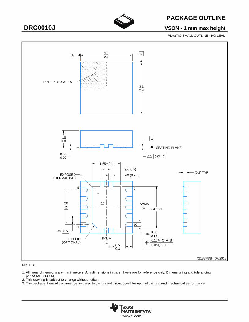
PACKAGE OUTLINE
C
10X 0.300.18
2.4 0.1
2X2
1.65 0.1
8X 0.5
1.00.8
10X 0.50.3
0.050.00
A 3.12.9
B
3.12.9
(0.2) TYP4X (0.25)
2X (0.5)
VSON - 1 mm max heightDRC0010JPLASTIC SMALL OUTLINE - NO LEAD
4218878/B 07/2018
PIN 1 INDEX AREA
SEATING PLANE
0.08 C
1
5 6
10
(OPTIONAL)PIN 1 ID 0.1 C A B
0.05 C
THERMAL PADEXPOSED
SYMM
SYMM11
NOTES: 1. All linear dimensions are in millimeters. Any dimensions in parenthesis are for reference only. Dimensioning and tolerancing per ASME Y14.5M. 2. This drawing is subject to change without notice. 3. The package thermal pad must be soldered to the printed circuit board for optimal thermal and mechanical performance.
SCALE 4.000

www.ti.com
EXAMPLE BOARD LAYOUT
0.07 MINALL AROUND0.07 MAX
ALL AROUND
10X (0.24)
(2.4)
(2.8)
8X (0.5)
(1.65)
( 0.2) VIATYP
(0.575)
(0.95)
10X (0.6)
(R0.05) TYP
(3.4)
(0.25)
(0.5)
VSON - 1 mm max heightDRC0010JPLASTIC SMALL OUTLINE - NO LEAD
4218878/B 07/2018
SYMM
1
5 6
10
LAND PATTERN EXAMPLEEXPOSED METAL SHOWN
SCALE:20X
11SYMM
NOTES: (continued) 4. This package is designed to be soldered to a thermal pad on the board. For more information, see Texas Instruments literature number SLUA271 (www.ti.com/lit/slua271).5. Vias are optional depending on application, refer to device data sheet. If any vias are implemented, refer to their locations shown on this view. It is recommended that vias under paste be filled, plugged or tented.
SOLDER MASKOPENINGSOLDER MASK
METAL UNDER
SOLDER MASKDEFINED
EXPOSED METAL
METALSOLDER MASKOPENING
SOLDER MASK DETAILS
NON SOLDER MASKDEFINED
(PREFERRED)
EXPOSED METAL

www.ti.com
EXAMPLE STENCIL DESIGN
(R0.05) TYP
10X (0.24)
10X (0.6)
2X (1.5)
2X(1.06)
(2.8)
(0.63)
8X (0.5)
(0.5)
4X (0.34)
4X (0.25)
(1.53)
VSON - 1 mm max heightDRC0010JPLASTIC SMALL OUTLINE - NO LEAD
4218878/B 07/2018
NOTES: (continued) 6. Laser cutting apertures with trapezoidal walls and rounded corners may offer better paste release. IPC-7525 may have alternate design recommendations.
SOLDER PASTE EXAMPLEBASED ON 0.125 mm THICK STENCIL
EXPOSED PAD 11:
80% PRINTED SOLDER COVERAGE BY AREASCALE:25X
SYMM
1
56
10
EXPOSED METALTYP11
SYMM

IMPORTANT NOTICE AND DISCLAIMERTI PROVIDES TECHNICAL AND RELIABILITY DATA (INCLUDING DATA SHEETS), DESIGN RESOURCES (INCLUDING REFERENCE DESIGNS), APPLICATION OR OTHER DESIGN ADVICE, WEB TOOLS, SAFETY INFORMATION, AND OTHER RESOURCES “AS IS” AND WITH ALL FAULTS, AND DISCLAIMS ALL WARRANTIES, EXPRESS AND IMPLIED, INCLUDING WITHOUT LIMITATION ANY IMPLIED WARRANTIES OF MERCHANTABILITY, FITNESS FOR A PARTICULAR PURPOSE OR NON-INFRINGEMENT OF THIRD PARTY INTELLECTUAL PROPERTY RIGHTS.These resources are intended for skilled developers designing with TI products. You are solely responsible for (1) selecting the appropriate TI products for your application, (2) designing, validating and testing your application, and (3) ensuring your application meets applicable standards, and any other safety, security, regulatory or other requirements.These resources are subject to change without notice. TI grants you permission to use these resources only for development of an application that uses the TI products described in the resource. Other reproduction and display of these resources is prohibited. No license is granted to any other TI intellectual property right or to any third party intellectual property right. TI disclaims responsibility for, and you will fully indemnify TI and its representatives against, any claims, damages, costs, losses, and liabilities arising out of your use of these resources.TI’s products are provided subject to TI’s Terms of Sale or other applicable terms available either on ti.com or provided in conjunction with such TI products. TI’s provision of these resources does not expand or otherwise alter TI’s applicable warranties or warranty disclaimers for TI products.TI objects to and rejects any additional or different terms you may have proposed. IMPORTANT NOTICE
Mailing Address: Texas Instruments, Post Office Box 655303, Dallas, Texas 75265Copyright © 2022, Texas Instruments Incorporated