SYNCHRONOUS PRESETTABLE 4-BIT COUNTER
16
M54/74HC160/161 M54/74HC162/163 April 1993 SYNCHRONOUS PRESETTABLE 4-BIT COUNTER B1R (Plastic Package) ORDER CODES : M54HCXXXF1R M74HCXXXM1R M74HCXXXB1R M74HCXXXC1R F1R (Ceramic Package) M1R (Micro Package) C1R (Chip Carrier) PIN CONNECTIONS (top view) NC = No Inter- nal Con- DESCRIPTION . HIGH SPEED fMAX = 63 MHz (TYP.) AT VCC =5V . LOW POWER DISSIPATION I CC =4 μA (MAX.) AT 25 °C . OUTPUT DRIVE CAPABILITY 10 LSTTL LOADS . BALANCED PROPAGATION DELAYS t PLH =t PHL . HIGH NOISE IMMUNITY VNIH =VNIL = 28 % VCC (MIN.) . WIDE OPERATING VOLTAGE RANGE V CC (OPR) = 2 V TO 6 V . PIN AND FUNCTION COMPATIBLE WITH 54/74LS160 ∼ 163 M54/74HC160 Decade, Asynchronous Clear M54/74HC161Binary, Asynchronous Clear M54/74HC162 Decade, Synchronous Clear M54/74HC163Binary, Synchronous Clear The M54/74HC160, 161, 162 and 163 are high speed CMOS SYNCHRONOUS PRESETTABLE COUNTERS fabricated with silicon gate C 2 MOS technology. They have the same the high speed operation simi- lar to equivalent LSTTL while maintaining the CMOS low power dissipation. The M54/74HC160/162 are BCDDecade counters and the M54/74HC161/163 are 4 bit binary counter- s. The CLOCK input is active on the rising edge. Both LOAD and CLEAR inputs are active Low. Presetting of all four IC’s is synchronous on the ris- ing edge of the CLOCK. The function on the M54/74HC162/163 is syn- chronous to CLOCK, while the M54/74HC160/161 counters are cleared asynchronously. Two enable inputs(TE and PE) and CARRYoutput are provided to enable easy cascading of counters, which facilities easy implementation of N-bit counters without using external gates. All inputs are equipped with protection circuits against staticdischarge and transient excess volt- age. 1/16
-
Upload
khangminh22 -
Category
Documents
-
view
5 -
download
0
Transcript of SYNCHRONOUS PRESETTABLE 4-BIT COUNTER

M54/74HC160/161M54/74HC162/163
April 1993
SYNCHRONOUS PRESETTABLE 4-BIT COUNTER
B1R(Plastic Package)
ORDER CODES :M54HCXXXF1R M74HCXXXM1RM74HCXXXB1R M74HCXXXC1R
F1R(Ceramic Package)
M1R(Micro Package)
C1R(Chip Carrier)
PIN CONNECTIONS (top view)
NC =No Inter-nal Con-
DESCRIPTION
.HIGH SPEEDfMAX = 63 MHz (TYP.) AT VCC = 5 V.LOW POWER DISSIPATIONICC = 4 µA (MAX.) AT 25 °C.OUTPUT DRIVE CAPABILITY10 LSTTL LOADS.BALANCED PROPAGATION DELAYStPLH = tPHL.HIGH NOISE IMMUNITYVNIH = VNIL = 28 % VCC (MIN.).WIDE OPERATING VOLTAGE RANGEVCC (OPR) = 2 V TO 6 V.PIN AND FUNCTION COMPATIBLEWITH 54/74LS160 ∼ 163
M54/74HC160 Decade, Asynchronous ClearM54/74HC161 Binary, Asynchronous ClearM54/74HC162 Decade, Synchronous ClearM54/74HC163 Binary, Synchronous Clear
The M54/74HC160, 161, 162 and 163 are highspeed CMOS SYNCHRONOUS PRESETTABLECOUNTERS fabricated with silicon gate C2MOStechnology.
They have the same the high speed operation simi-lar to equivalent LSTTL while maintaining theCMOS low power dissipation.
The M54/74HC160/162 are BCD Decade countersand the M54/74HC161/163 are 4 bit binary counter-s.
The CLOCK input is active on the rising edge. BothLOAD and CLEAR inputs are active Low.
Presetting of all four IC’s is synchronous on the ris-ing edge of the CLOCK.
The function on the M54/74HC162/163 is syn-chronous to CLOCK, while the M54/74HC160/161counters are cleared asynchronously.
Two enable inputs (TE and PE) and CARRYoutputare provided to enable easy cascading of counters,which facilities easy implementation of N-bitcounters without using external gates.
All inputs are equipped with protection circuitsagainst static discharge and transient excess volt-age.
1/16

INPUT AND OUTPUT EQUIVALENT CIRCUIT
IEC LOGIC SYMBOL (HC161)IEC LOGIC SYMBOL (HC160)
IEC LOGIC SYMBOL (HC162) IEC LOGIC SYMBOL (HC163)
PIN DESCRIPTION
PIN No SYMBOL NAME AND FUNCTION
1 CLEAR Asynchronous Masterreset
2 CLOCK Clock Input (LOW toHIGH, Edge-triggered)
3, 4, 5, 6 A, B, C, D Data Inputs
7 ENABLE P Count Enable Input
10 ENABLET Count Enable Carry Input
9 LOAD Parallel Enable Input
14, 13, 12,11
QA to QD Flip Flop Outputs
15 CARRYOUTPUT
Terminal Count Output
8 GND Ground (0V)
16 VCC Positive Supply Voltage
M54/M74HC160/161/162/163
2/16
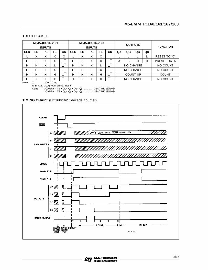
TRUTH TABLE
M54/74HC160/161 M54/74HC162/163OUTPUTS
FUNCTIONINPUTS INPUTS
CLR LD PE TE CK CLR LD PE TE CK QA QB QC QD
L X X X X L X X X L L L L RESET TO ”0”
H L X X H L X X A B C D PRESET DATA
H H X L H H X L NO CHANGE NO COUNT
H H L X H H L X NO CHANGE NO COUNT
H H H H H H H H COUNT UP COUNT
H X X X X X X X NO CHANGE NO COUNTNote: X : Don’t Care
A, B, C, D : Logi level of data inputsCarry : CARRY = TE • QA • QB • QC • QD ............ (M54/74HC160/162)
: CARRY = TE • QA • QB • QC • QD ............ (M54/74HC161/163)
TIMING CHART (HC160/162 : decade counter)
M54/M74HC160/161/162/163
3/16

TIMING CHART (HC161/163 : binary counter)
M54/M74HC160/161/162/163
4/16

LOGIC DIAGRAM
LOGIC DIAGRAM
HC160
HC161
M54/M74HC160/161/162/163
5/16

LOGIC DIAGRAM
LOGIC DIAGRAM
HC163
HC162
M54/M74HC160/161/162/163
6/16

ABSOLUTE MAXIMUM RATINGS
Symbol Parameter Value Unit
VCC Supply Voltage -0.5 to +7 V
VI DC Input Voltage -0.5 to VCC + 0.5 V
VO DC Output Voltage -0.5 to VCC + 0.5 V
IIK DC Input Diode Current ± 20 mA
IOK DC Output Diode Current ± 20 mA
IO DC Output Source Sink Current Per Output Pin ± 25 mA
ICC or IGND DC VCC or Ground Current ± 50 mA
PD Power Dissipation 500 (*) mW
Tstg Storage Temperature -65 to +150 oC
TL Lead Temperature (10 sec) 300 oCAbsolute MaximumRatings are those values beyond whichdamage to the device may occur. Functional operation under these condition isnot implied.(*) 500 mW: ≅ 65 oC derate to 300 mW by 10mW/oC: 65 oC to 85 oC
RECOMMENDED OPERATING CONDITIONS
Symbol Parameter Value Unit
VCC Supply Voltage 2 to 6 V
VI Input Voltage 0 to VCC V
VO Output Voltage 0 to VCC V
Top Operating Temperature: M54HC SeriesM74HC Series
-55 to +125-40 to +85
oCoC
tr, tf Input Rise and Fall Time VCC = 2 V 0 to 1000 ns
VCC = 4.5 V 0 to 500
VCC = 6 V 0 to 400
M54/M74HC160/161/162/163
7/16

DC SPECIFICATIONS
Symbol Parameter
Test Conditions Value
UnitVCC
(V)
TA = 25 oC54HC and 74HC
-40 to 85 oC74HC
-55 to 125 oC54HC
Min. Typ. Max. Min. Max. Min. Max.
VIH High Level InputVoltage
2.0 1.5 1.5 1.5V4.5 3.15 3.15 3.15
6.0 4.2 4.2 4.2
VIL Low Level InputVoltage
2.0 0.5 0.5 0.5V4.5 1.35 1.35 1.35
6.0 1.8 1.8 1.8
VOH High LevelOutput Voltage
2.0VI =VIH
orVIL
IO=-20 µA1.9 2.0 1.9 1.9
V4.5 4.4 4.5 4.4 4.4
6.0 5.9 6.0 5.9 5.9
4.5 IO=-4.0 mA 4.18 4.31 4.13 4.10
6.0 IO=-5.2 mA 5.68 5.8 5.63 5.60
VOL Low Level OutputVoltage
2.0VI =VIH
orVIL
IO= 20 µA0.0 0.1 0.1 0.1
V4.5 0.0 0.1 0.1 0.1
6.0 0.0 0.1 0.1 0.1
4.5 IO= 4.0 mA 0.17 0.26 0.33 0.40
6.0 IO= 5.2 mA 0.18 0.26 0.33 0.40
II Input LeakageCurrent
6.0VI = VCC or GND ±0.1 ±1 ±1 µA
ICC Quiescent SupplyCurrent
6.0 VI = VCC or GND 4 40 80 µA
M54/M74HC160/161/162/163
8/16

AC ELECTRICAL CHARACTERISTICS (CL = 50 pF, Input tr = tf = 6 ns)
Symbol Parameter
Test Conditions Value
UnitVCC
(V)
TA = 25 oC54HC and 74HC
-40 to 85 oC74HC
-55 to 125 oC54HC
Min. Typ. Max. Min. Max. Min. Max.tTLH
tTHL
Output TransitionTime
2.0 25 75 95 110ns4.5 7 15 19 22
6.0 6 13 16 19
tPLH
tPHL
PropagationDelay Time(CLOCK - Q)
2.0 48 125 155 190ns4.5 16 25 31 38
6.0 14 21 26 32
tPLH
tPHL
PropagationDelay Time(CLOCK-CARRY)
2.0COUNT MODE
57 150 190 225ns4.5 19 30 38 45
6.0 16 26 32 38
tPLH PropagationDelay Time(CLOCK-CARRY)
2.0PRESET MODE
66 175 220 265ns4.5 22 35 44 53
6.0 19 30 37 45
tPHL PropagationDelay Time(CLOCK-CARRY)
2.0PRESET MODE
72 200 250 300ns4.5 24 40 50 60
6.0 20 34 43 51
tPLH
tPHL
PropagationDelay Time(ENT-CARRY)
2.0 39 100 125 150ns4.5 13 20 25 30
6.0 11 17 21 26
tPLH PropagationDelay Time(CLEAR - Q)
2.0 forHC160/161
only
60 150 190 225ns4.5 20 30 38 45
6.0 17 26 32 38
tPHL PropagationDelay Time(CLEAR-CARRY)
2.0 forHC160/161
only
72 200 250 300ns4.5 24 40 50 60
6.0 20 34 43 51
fMAX Maximum ClockFrequency
2.0 6.2 18 5 4.2MHz4.5 31 53 25 21
6.0 37 62 30 25
tW(H)
tW(L)
Minimum PulseWidth(CLOCK)
2.0 18 75 95 110ns4.5 6 15 19 22
6.0 6 13 16 19
tW(L) Minimum PulseWidth(CLEAR)
2.0 forHC160/161
only
24 75 95 110ns4.5 7 15 19 22
6.0 6 13 16 19
ts Minimum Set-upTime(LOAD, PE, TE)
2.0 40 100 125 150ns4.5 10 20 25 30
6.0 8 17 21 26
ts Minimum Set-upTime(A, B, C, D)
2.0 20 75 95 110ns4.5 5 15 19 22
6.0 3 13 16 19
ts Minimum Set-upTime(CLEAR)
2.0 forHC162/163
only
20 75 95 110ns4.5 5 15 19 22
6.0 3 13 16 19
M54/M74HC160/161/162/163
9/16
AC ELECTRICAL CHARACTERISTICS (CL = 50 pF, Input tr = tf = 6 ns)
Symbol Parameter
Test Conditions Value
UnitVCC
(V)
TA = 25 oC54HC and 74HC
-40 to 85 oC74HC
-55 to 125 oC54HC
Min. Typ. Max. Min. Max. Min. Max.th Minimum Hold
Time(A, B - CK)
2.0 0 0 0ns4.5 0 0 0
6.0 0 0 0
tREM MinimumRemoval Time
2.0 18 50 65 75ns4.5 4 10 13 15
6.0 3 9 11 13
CIN Input Capacitance 5 10 10 10 pF
CPD (*) Power DissipationCapacitance
50pF
(*) CPD is defined as the value of the IC’s internal equivalent capacitance which is calculated from the operating current consumption without load.(Refer to Test Circuit). Average operting current can be obtained by the followingequation. ICC(opr) = CPD • VCC • fIN + ICC
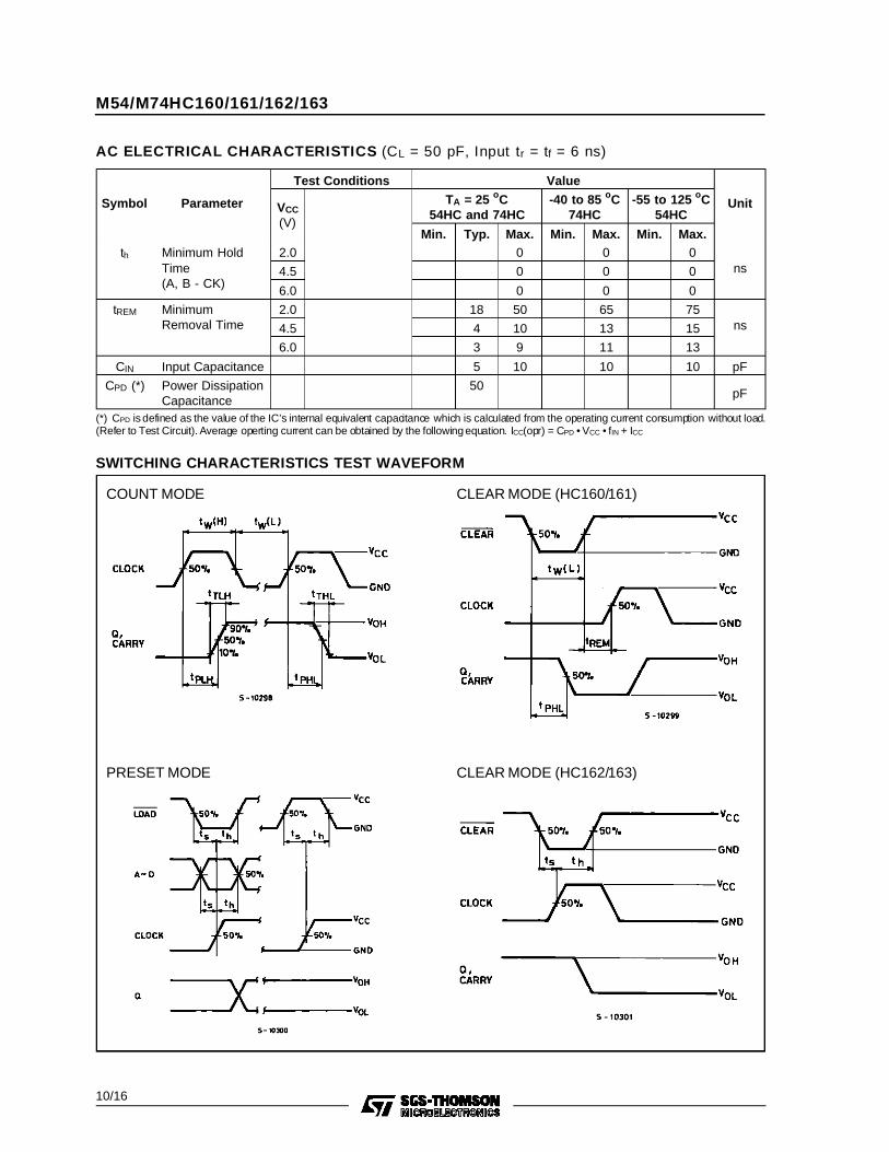
SWITCHING CHARACTERISTICS TEST WAVEFORM
COUNT MODE CLEAR MODE (HC160/161)
PRESET MODE CLEAR MODE (HC162/163)
M54/M74HC160/161/162/163
10/16
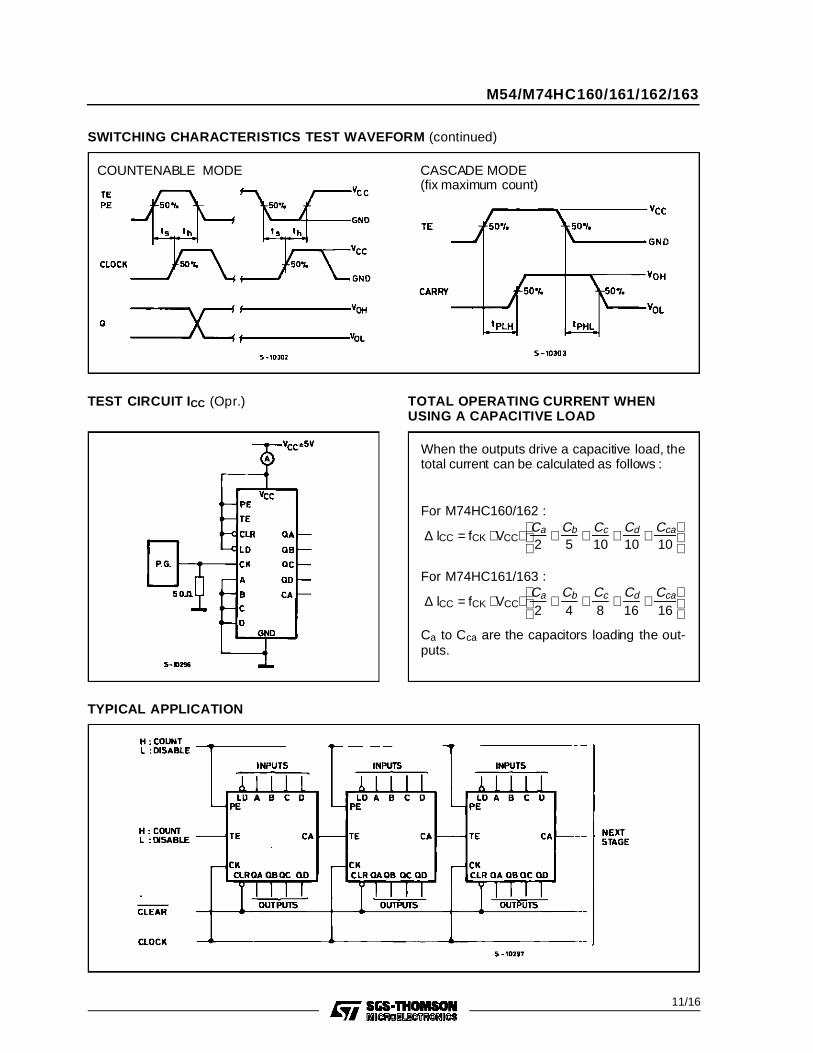
TEST CIRCUIT ICC (Opr.)
SWITCHING CHARACTERISTICS TEST WAVEFORM (continued)
TOTAL OPERATING CURRENT WHENUSING A CAPACITIVE LOAD
TYPICAL APPLICATION
COUNTENABLE MODE CASCADE MODE(fix maximum count)
When the outputs drive a capacitive load, thetotal current can be calculated as follows :
For M74HC160/162 :
∆ lCC = fCK ⋅ VCC⋅ Ca
2+ Cb
5+ Cc
10+ Cd
10+ Cca
10
For M74HC161/163 :
∆ lCC = fCK ⋅ VCC⋅
Ca
2+
Cb
4+
Cc
8+
Cd
16+
Cca
16
Ca to Cca are the capacitors loading the out-puts.
M54/M74HC160/161/162/163
11/16

Plastic DIP16 (0.25) MECHANICAL DATA
DIM.mm inch
MIN. TYP. MAX. MIN. TYP. MAX.
a1 0.51 0.020
B 0.77 1.65 0.030 0.065
b 0.5 0.020
b1 0.25 0.010
D 20 0.787
E 8.5 0.335
e 2.54 0.100
e3 17.78 0.700
F 7.1 0.280
I 5.1 0.201
L 3.3 0.130
Z 1.27 0.050
P001C
M54/M74HC160/161/162/163
12/16
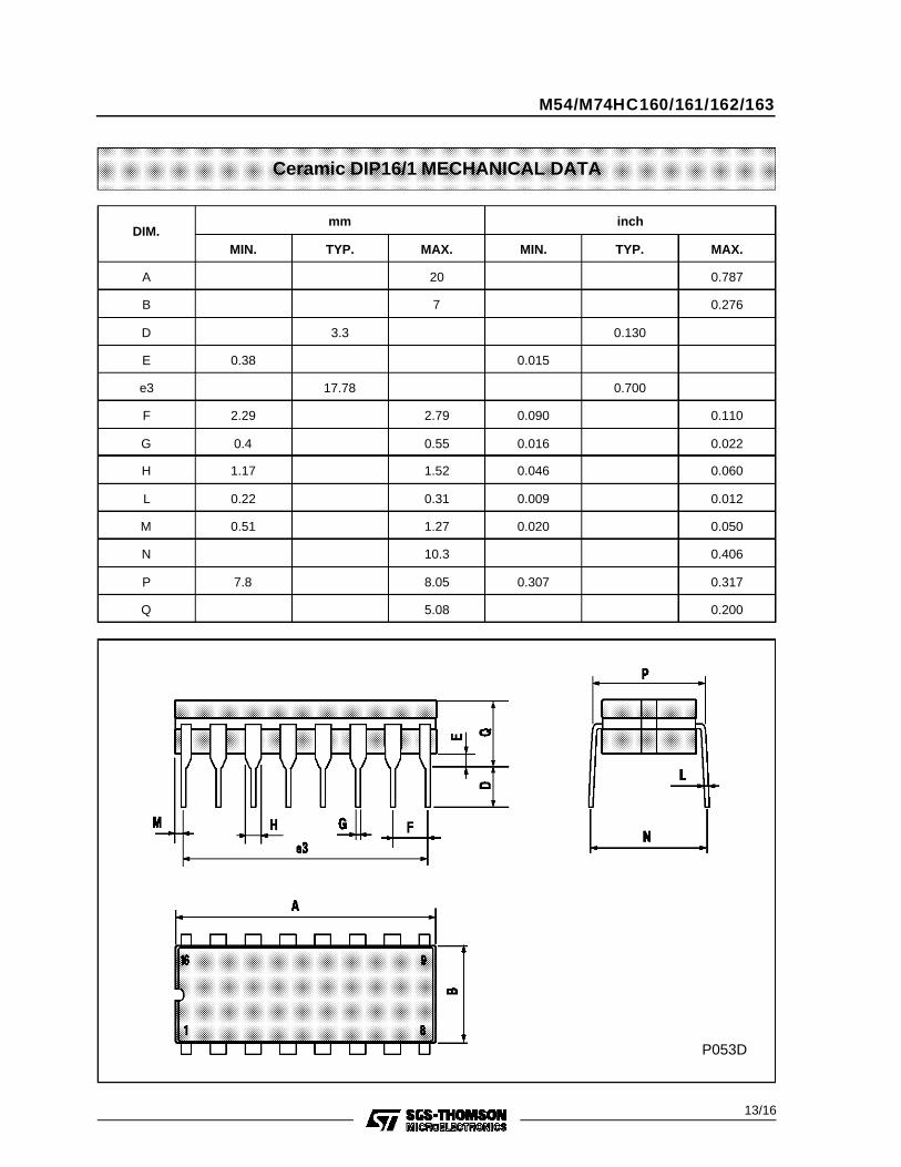
Ceramic DIP16/1 MECHANICAL DATA
DIM.mm inch
MIN. TYP. MAX. MIN. TYP. MAX.
A 20 0.787
B 7 0.276
D 3.3 0.130
E 0.38 0.015
e3 17.78 0.700
F 2.29 2.79 0.090 0.110
G 0.4 0.55 0.016 0.022
H 1.17 1.52 0.046 0.060
L 0.22 0.31 0.009 0.012
M 0.51 1.27 0.020 0.050
N 10.3 0.406
P 7.8 8.05 0.307 0.317
Q 5.08 0.200
P053D
M54/M74HC160/161/162/163
13/16

SO16 (Narrow) MECHANICAL DATA
DIM.mm inch
MIN. TYP. MAX. MIN. TYP. MAX.
A 1.75 0.068
a1 0.1 0.2 0.004 0.007
a2 1.65 0.064
b 0.35 0.46 0.013 0.018
b1 0.19 0.25 0.007 0.010
C 0.5 0.019
c1 45° (typ.)
D 9.8 10 0.385 0.393
E 5.8 6.2 0.228 0.244
e 1.27 0.050
e3 8.89 0.350
F 3.8 4.0 0.149 0.157
G 4.6 5.3 0.181 0.208
L 0.5 1.27 0.019 0.050
M 0.62 0.024
S 8° (max.)
P013H
M54/M74HC160/161/162/163
14/16

PLCC20 MECHANICAL DATA
DIM.mm inch
MIN. TYP. MAX. MIN. TYP. MAX.
A 9.78 10.03 0.385 0.395
B 8.89 9.04 0.350 0.356
D 4.2 4.57 0.165 0.180
d1 2.54 0.100
d2 0.56 0.022
E 7.37 8.38 0.290 0.330
e 1.27 0.050
e3 5.08 0.200
F 0.38 0.015
G 0.101 0.004
M 1.27 0.050
M1 1.14 0.045
P027A
M54/M74HC160/161/162/163
15/16

Information furnished is believed to be accurate and reliable. However, SGS-THOMSON Microelectronics assumes no responsability for theconsequences of use of such information nor for any infringement of patents or other rights of third parties which may results from its use. Nolicense is granted by implication or otherwise under any patent or patent rights of SGS-THOMSON Microelectronics. Specificationsmentionedin this publication are subject to change without notice. This publication supersedes and replaces all information previously supplied.SGS-THOMSON Microelectronicsproducts are not authorized foruse ascritical components in life support devices or systems without expresswritten approval of SGS-THOMSON Microelectonics.
1994 SGS-THOMSON Microelectronics - All Rights Reserved
SGS-THOMSON Microelectronics GROUP OF COMPANIESAustralia - Brazil - France - Germany - Hong Kong - Italy - Japan - Korea - Malaysia - Malta - Morocco - The Netherlands -
Singapore - Spain - Sweden - Switzerland - Taiwan - Thailand - United Kingdom - U.S.A
M54/M74HC160/161/162/163
16/16