32 Bit RISC Microcontroller TMPM374FWUG
608
32 Bit RISC Microcontroller TX03 Series TMPM374FWUG
-
Upload
khangminh22 -
Category
Documents
-
view
1 -
download
0
Transcript of 32 Bit RISC Microcontroller TMPM374FWUG

32 Bit RISC MicrocontrollerTX03 Series
TMPM374FWUG

© 2011 TOSHIBA CORPORATION All Rights Reserved

************************************************************************************************************************* ARM, Cortex and Thumb are registered trademarks of ARM Limited (or its subsidiaries) in the EU
and/or elsewhere. All rights reserved.*************************************************************************************************************************
R
TMPM374FWUG

General precautions on the use of Toshiba MCUs
This Page explains general precautions on the use of Toshiba MCUs.
Note that if there is a difference between the general precautions and the description in the body of the docu-ment, the description in the body of document has higher priority.
1. The MCUs’ operation at power-on
At power-on, internal state of the MCUs is unstable. Therefore, state of the pins is undefined until re-set operation is completed.
When a reset is performed by an external reset pin, pins of the MCUs that use the reset pin are unde-fined until reset operation by the external pin is completed.
Also, when a reset is performed by the internal power-on reset, pins of the MCUs that use the internalpower-on reset are undefined until power supply voltage reaches the voltage at which power-on reset is val-id.
2. Unused pins
Unused input/output ports of the MCUs are prohibited to use. The pins are high-impedance.
Generally, if MCUs operate while the high-impedance pins left open, electrostatic damage or latch-upmay occur in the internal LSI due to induced voltage influenced from external noise.
Toshiba recommend that each unused pin should be connected to the power supply pins or GND pinsvia resistors.
3. Clock oscillation stability
A reset state must be released after the clock oscillation becomes stable. If the clock is changed to anoth-er clock while the program is in progress, wait until the clock is stable.
TMPM374FWUG
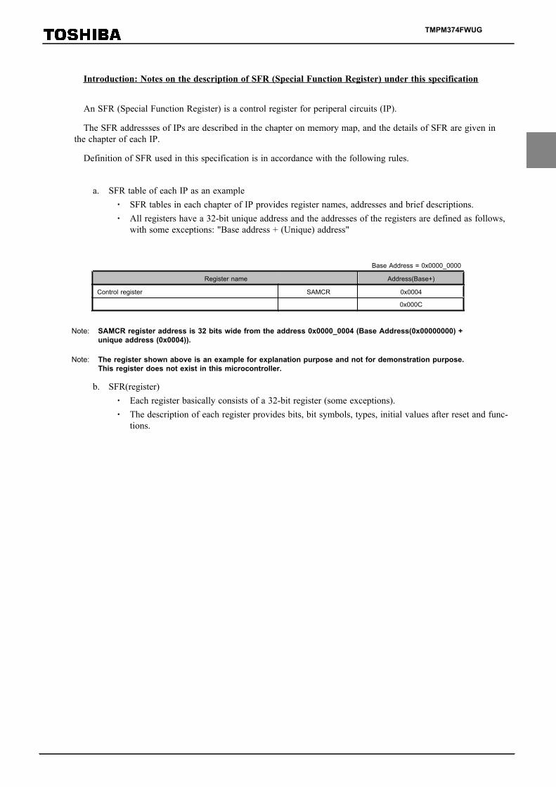
Introduction: Notes on the description of SFR (Special Function Register) under this specification
An SFR (Special Function Register) is a control register for periperal circuits (IP).
The SFR addressses of IPs are described in the chapter on memory map, and the details of SFR are given inthe chapter of each IP.
Definition of SFR used in this specification is in accordance with the following rules.
a. SFR table of each IP as an example・ SFR tables in each chapter of IP provides register names, addresses and brief descriptions.・ All registers have a 32-bit unique address and the addresses of the registers are defined as follows,
with some exceptions: "Base address + (Unique) address"
Base Address = 0x0000_0000
Register name Address(Base+)
Control register SAMCR 0x0004
0x000C
Note: SAMCR register address is 32 bits wide from the address 0x0000_0004 (Base Address(0x00000000) +unique address (0x0004)).
Note: The register shown above is an example for explanation purpose and not for demonstration purpose.This register does not exist in this microcontroller.
b. SFR(register)・ Each register basically consists of a 32-bit register (some exceptions).・ The description of each register provides bits, bit symbols, types, initial values after reset and func-
tions.
TMPM374FWUG

1.2.2 SAMCR(Control register)
31 30 29 28 27 26 25 24
bit symbol - - - - - - - -
After reset 0 0 0 0 0 0 0 0
23 22 21 20 19 18 17 16
bit symbol - - - - - - - -
After reset 0 0 0 0 0 0 0 0
15 14 13 12 11 10 9 8
bit symbol - - - - - - MODE
After reset 0 0 0 0 0 0 0 0
7 6 5 4 3 2 1 0
bit symbol MODE TDATA
After reset 0 0 0 1 0 0 0 0
Bit Bit Symbol Type Function
31-10 − R "0" can be read.
9-7 MODE[2:0] R/W Operation mode settings000 : Sample mode 0001 : Sample mode 1010 : Sample mode 2011 : Sample mode 3The settings other than those above: Reserved
6-0 TDATA[6:0] W Transmitted data
Note: The Type is divided into three as shown below.
R / W READ WRITE
R READ
W WRITE
c. Data descriptopn
Meanings of symbols used in the SFR description are as shown below.・ x:channel numbers/ports・ n,m:bit numbers
d. Register descriptoption
Registers are described as shown below.・ Register name <Bit Symbol>
Exmaple: SAMCR<MODE>="000" or SAMCR<MODE[2:0]>="000"
<MODE[2:0]> indicates bit 2 to bit 0 in bit symbol mode (3bit width).・ Register name [Bit]
Example: SAMCR[9:7]="000"
It indicates bit 9 to bit 7 of the register SAMCR (32 bit width).
TMPM374FWUG

Revision History
Date Revision Comment
2011/8/1 1 First Release
2013/4/15 2 Contents Revised
2014/12/19 3 Contents Revised

Table of Contents
General precautions on the use of Toshiba MCUs
TMPM374FWUG
1.1 Features......................................................................................................................................11.2 Block Diagram...........................................................................................................................51.3 Pin Layout (Top view)..............................................................................................................61.4 Pin names and Functions...........................................................................................................7
1.4.1 Sorted by Port......................................................................................................................................................................71.5 Pin Numbers and Power Supply Pins.....................................................................................10
2. Processor Core
2.1 Information on the processor core..........................................................................................112.2 Configurable Options..............................................................................................................112.3 Exceptions/ Interruptions.........................................................................................................12
2.3.1 Number of Interrupt Inputs...............................................................................................................................................122.3.2 Number of Priority Level Interrupt Bits...........................................................................................................................122.3.3 SysTick..............................................................................................................................................................................122.3.4 SYSRESETREQ................................................................................................................................................................122.3.5 LOCKUP...........................................................................................................................................................................122.3.6 Auxiliary Fault Status register..........................................................................................................................................12
2.4 Events......................................................................................................................................132.5 Power Management.................................................................................................................132.6 Exclusive access......................................................................................................................13
3. Memory Map
3.1 Memory Map...........................................................................................................................153.1.1 TMPM374FWUGMemory Map........................................................................................................................................15
3.2 Details of SFR area.................................................................................................................16
4. Reset operation
4.1 Initial state...............................................................................................................................174.2 Reset operation........................................................................................................................174.3 After Reset...............................................................................................................................17
5. Clock / Mode Control
i
5.1 Features....................................................................................................................................195.2 Registers..................................................................................................................................20
5.2.1 Register List.......................................................................................................................................................................205.2.2 CGSYSCR (System control register)................................................................................................................................215.2.3 CGOSCCR (Oscillation control register).........................................................................................................................225.2.4 CGSTBYCR (Standby control register)...........................................................................................................................245.2.5 CGPLLSEL (PLL Selection Register)..............................................................................................................................25
5.3 Clock control...........................................................................................................................265.3.1 Clock Type........................................................................................................................................................................265.3.2 Initial Values after Reset...................................................................................................................................................265.3.3 Clock system Diagram......................................................................................................................................................275.3.4 Clock Multiplication Circuit (PLL)..................................................................................................................................28
5.3.4.1 The sequence of PLL setting5.3.5 Warm-up function..............................................................................................................................................................305.3.6 System Clock.....................................................................................................................................................................325.3.7 Prescaler Clock Control.....................................................................................................................................................33
5.4 Modes and Mode Transitions..................................................................................................345.4.1 Mode Transitions...............................................................................................................................................................34
5.5 Operation Mode.......................................................................................................................355.5.1 NORMAL mode................................................................................................................................................................35
5.6 Low Power Consumption Modes............................................................................................365.6.1 IDLE Mode........................................................................................................................................................................365.6.2 STOP mode........................................................................................................................................................................375.6.3 Low power Consumption Mode Setting...........................................................................................................................385.6.4 Operational Status in Each Mode.....................................................................................................................................385.6.5 Releasing the Low Power Consumption Mode................................................................................................................395.6.6 Warm-up............................................................................................................................................................................415.6.7 Clock Operation in Mode Transition................................................................................................................................42
5.6.7.1 Transition of operation modes : NORMAL → STOP → NORMAL
6. Exceptions
6.1 Overview..................................................................................................................................436.1.1 Exception types..................................................................................................................................................................436.1.2 Handling Flowchart...........................................................................................................................................................44
6.1.2.1 Exception Request and Detection6.1.2.2 Exception Handling and Branch to the Interrupt Service Routine (Pre-emption)6.1.2.3 Executing an ISR6.1.2.4 Exception exit
6.2 Reset Exceptions.....................................................................................................................506.3 Non-Maskable Interrupts (NMI).............................................................................................506.4 SysTick....................................................................................................................................506.5 Interrupts..................................................................................................................................51
6.5.1 Interrupt Sources................................................................................................................................................................516.5.1.1 Interrupt route6.5.1.2 Generation of Interrupt Requests6.5.1.3 Transmission of Interrupt Requests6.5.1.4 Precautions when using external interrupt pins6.5.1.5 List of Interrupt Sources6.5.1.6 Active level
6.5.2 Interrupt Handling.............................................................................................................................................................566.5.2.1 Flowchart6.5.2.2 Preparation6.5.2.3 Detection by Clock Generator6.5.2.4 Detection by CPU6.5.2.5 CPU processing6.5.2.6 Interrupt Service Routine (ISR)
6.6 Exception / Interrupt-Related Registers..................................................................................636.6.1 Register List.......................................................................................................................................................................636.6.2 NVIC Registers..................................................................................................................................................................64
6.6.2.1 SysTick Control and Status Register6.6.2.2 SysTick Reload Value Register6.6.2.3 SysTick Correct Value Register
ii

6.6.2.4 SysTick Calibration Value Register6.6.2.5 Interrupt Set-Enable Register 16.6.2.6 Interrupt Set-Enable Register 26.6.2.7 Interrupt Set-Enable Register 36.6.2.8 Interrupt Clear-Enable Register 16.6.2.9 Interrupt Clear-Enable Register 26.6.2.10 Interrupt Clear-Enable Register 36.6.2.11 Interrupt Set-Pending Register 16.6.2.12 Interrupt Set-Pending Register 26.6.2.13 Interrupt Set-Pending Register 36.6.2.14 Interrupt Clear-Pending Register 16.6.2.15 Interrupt Clear-Pending Register 26.6.2.16 Interrupt Clear-Pending Register 36.6.2.17 Interrupt Priority Register6.6.2.18 Vector Table Offset Register6.6.2.19 Application Interrupt and Reset Control Register6.6.2.20 System Handler Priority Register6.6.2.21 System Handler Control and State Register
6.6.3 Clock generator registers...................................................................................................................................................986.6.3.1 CGIMCGB (CG Interrupt Mode Control Register B)6.6.3.2 CGIMCGD (CG Interrupt Mode Control Register D)6.6.3.3 CGICRCG (CG Interrupt Request Clear Register)6.6.3.4 CGNMIFLG (NMI Flag Register)6.6.3.5 CGRSTFLG (Reset Flag Register)
7. Internal High-speed Oscillation Adjustment Function
7.1 Structure.................................................................................................................................1077.2 Registers................................................................................................................................108
7.2.1 Register list...................................................................................................................................................................... 1087.2.2 TRMOSCPRO (Protect register).....................................................................................................................................1087.2.3 TRMOSCEN (Enable register).......................................................................................................................................1097.2.4 TRMOSCINIT (Initial trimming value monitor register)..............................................................................................1107.2.5 TRMOSCSET (Trimming value setting register)...........................................................................................................111
7.3 Operational Description.........................................................................................................1127.3.1 Outline.............................................................................................................................................................................1127.3.2 Adjustment range.............................................................................................................................................................1127.3.3 Internal Oscillation Frequency Measurement using TMRB...........................................................................................112
8. Input / Output Ports
8.1 Port Functions........................................................................................................................1138.1.1 Function list.....................................................................................................................................................................1138.1.2 Port Registers Outline.....................................................................................................................................................1158.1.3 Port States in STOP Mode..............................................................................................................................................116
8.2 Port functions.........................................................................................................................1178.2.1 Port A (PA4 to PA6).......................................................................................................................................................117
8.2.1.1 Port A Circuit Type8.2.1.2 Port A register8.2.1.3 PADATA (Port A data register)8.2.1.4 PACR (Port A output control register)8.2.1.5 PAFR1 (Port A function register 1)8.2.1.6 PAFR2 (Port A function register 2)8.2.1.7 PAOD (Port A open drain control register)8.2.1.8 PAPUP (Port A pull-up control register)8.2.1.9 PAPDN (Port A pull-down control register)8.2.1.10 PAIE (Port A input control register)
8.2.2 Port B (PB3 to PB6)........................................................................................................................................................1268.2.2.1 Port B Circuit Type8.2.2.2 Port B register8.2.2.3 PBDATA (Port B data register)8.2.2.4 PBCR (Port B output control register)8.2.2.5 PBFR1 (Port B function register 1)8.2.2.6 PBOD (Port B open drain control register)8.2.2.7 PBPUP (Port B pull-up control register)8.2.2.8 PBPDN (Port B pull-down control register)
iii

8.2.2.9 PBIE (Port B input control register)8.2.3 Port E (PE0 to PE2,PE4,PE6 to 7).................................................................................................................................131
8.2.3.1 Port E Circuit Type8.2.3.2 Port E register8.2.3.3 PEDATA (Port E data register)8.2.3.4 PECR (Port E output control register)8.2.3.5 PEFR1 (Port E function register 1)8.2.3.6 PEFR2 (Port E function register 2)8.2.3.7 PEOD (Port E open drain control register)8.2.3.8 PEPUP (Port E pull-up control register)8.2.3.9 PEPDN (Port E pull-down control register)8.2.3.10 PEIE (Port E input control register)
8.2.4 Port F (PF0, PF2 to PF4)................................................................................................................................................1408.2.4.1 Port F Circuit Type8.2.4.2 Port F register8.2.4.3 PFDATA (Port F data register)8.2.4.4 PFCR (Port F output control register)8.2.4.5 PFFR1 (Port F function register 1)8.2.4.6 PFFR2 (Port F function register 2)8.2.4.7 PFFR3 (Port F function register 3)8.2.4.8 PFOD (Port F open drain control register)8.2.4.9 PFPUP (Port F pull-up control register)8.2.4.10 PFPDN (Port F pull-down control register)8.2.4.11 PFIE (Port F input control register)
8.2.5 Port G (PG0 to PG7).......................................................................................................................................................1498.2.5.1 Port G Circuit Type8.2.5.2 Port G register8.2.5.3 PGDATA (Port G data register)8.2.5.4 PGCR (Port G output control register)8.2.5.5 PGFR1 (Port G function register 1)8.2.5.6 PGOD (Port G open drain control register)8.2.5.7 PGPUP (Port G pull-up control register)8.2.5.8 PGPDN (Port G pull-down control register)8.2.5.9 PGIE (Port G input control register)
8.2.6 Port I (PI3).......................................................................................................................................................................1548.2.6.1 Port I Circuit Type8.2.6.2 Port I register8.2.6.3 PIDATA (Port I data register)8.2.6.4 PICR (Port I output control register)8.2.6.5 PIOD (Port I open drain control register)8.2.6.6 PIPUP (Port I pull-up control register)8.2.6.7 PIPDN (Port I pull-down control register)8.2.6.8 PIIE (Port I input control register)
8.2.7 Port J (PJ0,PJ6 to PJ7)....................................................................................................................................................1588.2.7.1 Port J Circuit Type8.2.7.2 Port J register8.2.7.3 PJDATA (Port J data register)8.2.7.4 PJCR (Port J output control register)8.2.7.5 PJFR1 (Port J function register 1)8.2.7.6 PJOD (Port J open drain control register)8.2.7.7 PJPUP (Port J pull-up control register)8.2.7.8 PJPDN (Port J pull-down control register)8.2.7.9 PJIE (Port J input control register)
8.2.8 Port K (PK0 to PK1).......................................................................................................................................................1668.2.8.1 Port K Circuit Type8.2.8.2 Port K register8.2.8.3 PKDATA (Port K data register)8.2.8.4 PKCR (Port K output control register)8.2.8.5 PKFR1 (Port K function register 1)8.2.8.6 PKOD (Port K open drain control register)8.2.8.7 PKPUP (Port K pull-up control register)8.2.8.8 PKPDN (Port K pull-down control register)8.2.8.9 PKIE (Port K input control register)
8.2.9 Port M (PM0 to PM1).....................................................................................................................................................1718.2.9.1 Port M Circuit Type8.2.9.2 Port M register8.2.9.3 PMDATA (Port M data register)8.2.9.4 PMCR (Port M output control register)8.2.9.5 PMOD (Port M open drain control register)8.2.9.6 PMPUP (Port M pull-up control register)8.2.9.7 PMPDN (Port M pull-down control register)8.2.9.8 PMIE (Port M input control register)
8.3 Block Diagrams of Ports.......................................................................................................1758.3.1 Port Types........................................................................................................................................................................1758.3.2 Type T1............................................................................................................................................................................176
iv
8.3.3 Type T2............................................................................................................................................................................1778.3.4 Type T3............................................................................................................................................................................1788.3.5 Type T4............................................................................................................................................................................1798.3.6 Type T5............................................................................................................................................................................1808.3.7 Type T6............................................................................................................................................................................1818.3.8 Type T7............................................................................................................................................................................1828.3.9 Type T8............................................................................................................................................................................1838.3.10 Type T9..........................................................................................................................................................................1848.3.11 Type T10........................................................................................................................................................................1858.3.12 Type T11........................................................................................................................................................................1868.3.13 Type T12........................................................................................................................................................................1878.3.14 Type T13........................................................................................................................................................................1888.3.15 Type T14........................................................................................................................................................................1898.3.16 Type T15........................................................................................................................................................................1908.3.17 Type T16........................................................................................................................................................................1918.3.18 Type T17........................................................................................................................................................................1928.3.19 Type T18........................................................................................................................................................................1938.3.20 Type T19........................................................................................................................................................................1948.3.21 Type T20........................................................................................................................................................................1958.3.22 Type T21........................................................................................................................................................................196
8.4 Appendix Port Setting List....................................................................................................1978.4.1 Port A Setting..................................................................................................................................................................1978.4.2 Port B Setting..................................................................................................................................................................1988.4.3 Port E Setting..................................................................................................................................................................1998.4.4 Port F Setting...................................................................................................................................................................2008.4.5 Port G Setting..................................................................................................................................................................2018.4.6 Port I Setting....................................................................................................................................................................2028.4.7 Port J Setting...................................................................................................................................................................2038.4.8 Port K Setting..................................................................................................................................................................2048.4.9 Port M Setting.................................................................................................................................................................204
9. 16-bit Timer / Event Counters (TMRB)
9.1 Outline...................................................................................................................................2059.2 Differences in the Specifications..........................................................................................2069.3 Configuration.........................................................................................................................2079.4 Registers................................................................................................................................208
9.4.1 Register list according to channel...................................................................................................................................2089.4.2 TBxEN(Enable register)..................................................................................................................................................2099.4.3 TBxRUN(RUN register)..................................................................................................................................................2109.4.4 TBxCR(Control register).................................................................................................................................................2119.4.5 TBxMOD(Mode register)................................................................................................................................................2129.4.6 TBxFFCR(Flip-flop control register)..............................................................................................................................2139.4.7 TBxST(Status register)....................................................................................................................................................2149.4.8 TBxIM(Interrupt mask register)......................................................................................................................................2159.4.9 TBxUC(Up counter capture register)..............................................................................................................................2169.4.10 TBxRG0(Timer register 0)............................................................................................................................................2179.4.11 TBxRG1(Timer register 1)............................................................................................................................................2179.4.12 TBxCP0(Capture register 0)..........................................................................................................................................2189.4.13 TBxCP1(Capture register 1)..........................................................................................................................................218
9.5 Description of Operations for Each Circuit..........................................................................2199.5.1 Prescaler...........................................................................................................................................................................2199.5.2 Up-counter (UC)..............................................................................................................................................................2219.5.3 Timer registers (TBxRG0, TBxRG1).............................................................................................................................2219.5.4 Capture.............................................................................................................................................................................2219.5.5 Capture register (TBxCP0, TBxCP1).............................................................................................................................2219.5.6 Up counter capture register (TBxUC)............................................................................................................................2229.5.7 Comparators (CP0, CP1).................................................................................................................................................2229.5.8 Timer Flip-flop (TBxFF0)...............................................................................................................................................2229.5.9 Capture interrupt (INTCAPx0, INTCAPx1)...................................................................................................................222
9.6 Description of Operations for Each Mode............................................................................2239.6.1 16-bit Interval Timer Mode.............................................................................................................................................2239.6.2 16-bit Event Counter Mode.............................................................................................................................................223
v
9.6.3 16-bit PPG (Programmable Pulse Generation) Output Mode........................................................................................2249.6.4 External trigger Programmable Pulse Generation Output Mode (PPG)........................................................................226
9.7 Applications using the Capture Function..............................................................................2279.7.1 One-shot pulse output triggered by an external pulse....................................................................................................2279.7.2 Pulse width measurement................................................................................................................................................229
10. Serial Channel (SIO/UART)
10.1 Overview............................................................................................................................23110.2 Difference in the Specifications of SIO Modules...............................................................23110.3 Configuration.......................................................................................................................23210.4 Registers Description...........................................................................................................233
10.4.1 Registers List in Each Channel.....................................................................................................................................23310.4.2 SCxEN (Enable Register)..............................................................................................................................................23410.4.3 SCxBUF (Buffer Register)............................................................................................................................................23510.4.4 SCxCR (Control Register)............................................................................................................................................23610.4.5 SCxMOD0 (Mode Control Register 0).........................................................................................................................23710.4.6 SCxMOD1 (Mode Control Register 1).........................................................................................................................23810.4.7 SCxMOD2 (Mode Control Register 2).........................................................................................................................23910.4.8 SCxBRCR (Baud Rate Generator Control Register), SCxBRADD (Baud Rate Generator Control Register 2).......24110.4.9 SCxFCNF (FIFO Configuration Register)....................................................................................................................24310.4.10 SCxRFC (RX FIFO Configuration Register).............................................................................................................24410.4.11 SCxTFC (TX FIFO Configuration Register) (Note2)................................................................................................24510.4.12 SCxRST (RX FIFO Status Register)..........................................................................................................................24610.4.13 SCxTST (TX FIFO Status Register)...........................................................................................................................247
10.5 Operation in Each Mode.....................................................................................................24810.6 Data Format.........................................................................................................................249
10.6.1 Data Format List............................................................................................................................................................24910.6.2 Parity Control................................................................................................................................................................250
10.6.2.1 Transmission10.6.2.2 Receiving Data
10.6.3 STOP Bit Length...........................................................................................................................................................25010.7 Clock Control......................................................................................................................251
10.7.1 Prescaler.........................................................................................................................................................................25110.7.2 Serial Clock Generation Circuit....................................................................................................................................253
10.7.2.1 Baud Rate Generator10.7.2.2 Clock Selection Circuit
10.8 Transmit/Receive Buffer and FIFO....................................................................................25810.8.1 Configuration.................................................................................................................................................................25810.8.2 Transmit/Receive Buffer...............................................................................................................................................25810.8.3 FIFO...............................................................................................................................................................................259
10.9 Status Flag...........................................................................................................................25910.10 Error Flag...........................................................................................................................259
10.10.1 OERR Flag..................................................................................................................................................................26010.10.2 PERR Flag...................................................................................................................................................................26010.10.3 FERR Flag...................................................................................................................................................................260
10.11 Receive..............................................................................................................................26110.11.1 Receive Counter..........................................................................................................................................................26110.11.2 Receive Control Unit...................................................................................................................................................261
10.11.2.1 I/O interface mode10.11.2.2 UART Mode
10.11.3 Receive Operation.......................................................................................................................................................26110.11.3.1 Receive Buffer10.11.3.2 Receive FIFO Operation10.11.3.3 I/O interface mode with SCLK output10.11.3.4 Read Received Data10.11.3.5 Wake-up Function10.11.3.6 Overrun Error
10.12 Transmission......................................................................................................................26510.12.1 Transmission Counter..................................................................................................................................................26510.12.2 Transmission Control..................................................................................................................................................265
10.12.2.1 I/O Interface Mode
vi

10.12.2.2 UART Mode10.12.3 Transmit Operation......................................................................................................................................................266
10.12.3.1 Operation of Transmission Buffer10.12.3.2 Transmit FIFO Operation10.12.3.3 I/O interface Mode/Transmission by SCLK Output10.12.3.4 Under-run error
10.13 Handshake function...........................................................................................................26910.14 Interrupt/Error Generation Timing....................................................................................270
10.14.1 RX Interrupts...............................................................................................................................................................27010.14.1.1 Single Buffer / Double Buffer10.14.1.2 FIFO
10.14.2 TX interrupts................................................................................................................................................................27110.14.2.1 Single Buffer / Double Buffer10.14.2.2 FIFO
10.14.3 Error Generation..........................................................................................................................................................27210.14.3.1 UART Mode10.14.3.2 IO Interface Mode
10.15 Software Reset...................................................................................................................27210.16 Operation in Each Mode...................................................................................................273
10.16.1 Mode 0 (I/O interface mode)......................................................................................................................................27310.16.1.1 Transmitting Data10.16.1.2 Receive10.16.1.3 Transmit and Receive (Full-duplex)
10.16.2 Mode 1 (7-bit UART mode).......................................................................................................................................28410.16.3 Mode 2 (8-bit UART mode).......................................................................................................................................28410.16.4 Mode 3 (9-bit UART mode).......................................................................................................................................285
10.16.4.1 Wake up function10.16.4.2 Protocol
11. 12-Bit Analog-to-Digital Converter
11.1 Functions and features.........................................................................................................28711.2 Block Diagram.....................................................................................................................28711.3 List of Registers...................................................................................................................28811.4 Register Descriptions...........................................................................................................290
11.4.1 ADBCLK (Clock Setting Register)..............................................................................................................................29011.4.2 ADBMOD0 (Mode Setting Register 0) .......................................................................................................................29111.4.3 ADBMOD1 (Mode Setting Register 1) .......................................................................................................................29211.4.4 ADBMOD2 (Mode Setting Register 2) .......................................................................................................................29311.4.5 ADBCMPCR0(Monitoring Setting Register 0)............................................................................................................29411.4.6 ADBCMPCR1(Monitoring Setting Register 1)............................................................................................................29511.4.7 ADBCMP0(Conversion Result Compare Register 0)..................................................................................................29611.4.8 ADBCMP1(Conversion Result Compare Register 1)..................................................................................................29611.4.9 ADBREG0(Conversion Result Register 0)...................................................................................................................29711.4.10 ADBREG1(Conversion Result Register 1).................................................................................................................29811.4.11 ADBREG2(Conversion Result Register 2).................................................................................................................29911.4.12 ADBREG3(Conversion Result Register 3).................................................................................................................30011.4.13 ADBREG4(Conversion Result Register 4).................................................................................................................30111.4.14 ADBREG5(Conversion Result Register 5).................................................................................................................30211.4.15 ADBREG6(Conversion Result Register 6).................................................................................................................30311.4.16 ADxBREG7(Conversion Result Register 7)...............................................................................................................30411.4.17 ADBREG8(Conversion Result Register 8).................................................................................................................30511.4.18 ADBREG9(Conversion Result Register 9).................................................................................................................30611.4.19 ADBREG10(Conversion Result Register 10).............................................................................................................30711.4.20 ADBREG11(Conversion Result Register 11).............................................................................................................30811.4.21 PMD Trigger Program Registers................................................................................................................................309
11.4.21.1 ADBPSEL6 to ADBPSEL11(PMD Trigger Program Number Select Register 6 to 11)11.4.21.2 ADBPINTS0 to 5(PMD Trigger Interrupt Select Register 0 to 5)11.4.21.3 ADBPSET0 to 5(PMD Trigger Program Register 0 to 5)
11.4.22 ADBTSET03 / ADBTSET47 / ADBTSET811 (Timer Trigger Program Registers) ...............................................32711.4.23 ADBSSET03 / ADBSSET47 / ADBSSET811( Software Trigger Program Registers )...........................................33111.4.24 ADBASET03 / ADBASET47 / ADBASET811( Constant Conversion Program Registers )...................................335
11.5 Operation Descriptions........................................................................................................33911.5.1 Analog Reference Voltages...........................................................................................................................................339
vii
11.5.2 Starting AD Conversion................................................................................................................................................33911.5.3 AD Conversion Monitoring Function...........................................................................................................................340
11.6 Timing chart of AD conversion..........................................................................................34111.6.1 Software trigger Conversion.........................................................................................................................................34111.6.2 Constant Conversion......................................................................................................................................................34211.6.3 AD conversion by trigger..............................................................................................................................................343
12. Motor Control Circuit (PMD: Programmable Motor Driver)
12.1 PMD Input/Output Signals..................................................................................................34612.2 PMD Circuit........................................................................................................................34712.3 PMD Registers.....................................................................................................................348
12.3.1 PMD1MDEN(PMD Enable Register)...........................................................................................................................34912.3.2 PMD1PORTMD(Port Output Mode Register).............................................................................................................35012.3.3 PMD1MODESEL (Mode Select Register)...................................................................................................................35112.3.4 Pulse Width Modulation Circuit...................................................................................................................................352
12.3.4.1 PMD1MDCR (PMD Control Register)12.3.4.2 PMD1CNTSTA (PWM Counter Status Register)12.3.4.3 PMD1MDCNT(PWM Counter Register)12.3.4.4 PMD1MDPRD(PWM Period Register)12.3.4.5 PMD1CMPU ( PWM Compare Registers of U Phase )12.3.4.6 PMD1CMPV (PWM Compare Registers of V Phase)12.3.4.7 PMD1CMPW (PWM Compare Registers of W Phase)
12.3.5 Conduction Control Circuit...........................................................................................................................................36212.3.5.1 PMD1MDPOT (PMD Output Setting Register)12.3.5.2 PMD1MDOUT(PMD Output Control Register)
12.3.6 Protection Control Circuit.............................................................................................................................................36612.3.6.1 EMG Protection Circuit12.3.6.2 PMD1EMGREL (EMG Release Register)12.3.6.3 PMD1EMGCR (EMG Control Register)12.3.6.4 PMD1EMGSTA (EMG Status Register)12.3.6.5 OVV Protection Control Circuit (OVV Block)12.3.6.6 PMD1OVVCR (OVV Control Register)12.3.6.7 PMD1OVVSTA (OVV Status Register)
12.3.7 Dead Time Circuit.........................................................................................................................................................37512.3.7.1 PMD1DTR (Dead Time Register )
12.3.8 Sync Trigger Generation Circuit...................................................................................................................................37712.3.8.1 PMD1TRGCMP0 (Trigger Compare Registers 0)12.3.8.2 PMD1TRGCMP1 (Trigger Compare Registers1)12.3.8.3 PMD1TRGCMP2 (Trigger Compare Registers 2)12.3.8.4 PMD1TRGCMP3 (Trigger Compare Registers 3)12.3.8.5 PMD1TRGCR (Trigger Control Register )12.3.8.6 PMD1TRGMD (Trigger Output Mode Setting Register)12.3.8.7 PMD1TRGSEL (Trigger Output Select Register)
13. Vector Engine (VE)
13.1 Overview..............................................................................................................................38713.1.1 Features..........................................................................................................................................................................38713.1.2 Key Specifications.........................................................................................................................................................388
13.2 Configuration.......................................................................................................................38813.2.1 Interaction among Vector Engine, Motor Control Circuit and A/D Converter...........................................................389
13.3 List of Registers...................................................................................................................39113.3.1 List of Registers............................................................................................................................................................39113.3.2 VE Control Registers....................................................................................................................................................394
13.3.2.1 VEEN (VE enable/disable register)13.3.2.2 VECPURUNTRG (CPU start trigger selection register)13.3.2.3 VETASKAPP(Task selection register)13.3.2.4 VEACTSCH (Operation schedule selection register)13.3.2.5 VEREPTIME (Schedule repeat count)13.3.2.6 VETRGMODE (Start trigger mode)13.3.2.7 VEERRINTEN (Error interrupt enable/disable)13.3.2.8 VECOMPEND (VE forced termination)13.3.2.9 VEERRDET (Error detection)13.3.2.10 VESCHTASKRUN (Schedule executing flag/executing task)
viii

13.3.2.11 VETMPREG0 (Temporary register 0)13.3.2.12 VETMPREG1 (Temporary register 1)13.3.2.13 VETMPREG2 (Temporary register 2)13.3.2.14 VETMPREG3 (Temporary register 3)13.3.2.15 VETMPREG4 (Temporary register 4)13.3.2.16 VETMPREG5 (Temporary register 5)
13.3.3 Common Registers........................................................................................................................................................40713.3.3.1 VETADC (Common ADC conversion time)
13.3.4 Channel-Specific Registers............................................................................................................................................40813.3.4.1 VEMODE1 (Task control mode Registers)13.3.4.2 VEFMODE1(Flow control Register)13.3.4.3 VETPWM1(PWM period rate control Register)13.3.4.4 VEOMEGA1(Rotation speed control Register)13.3.4.5 VETHETA1(Motor phase control Register)13.3.4.6 VECOS1/VESIN1/VECOSM1/VESINM113.3.4.7 VEIDREF1/VEIQREF1(dq Current Reference Registers)13.3.4.8 VEVD1/VEVQ1(d-axis/q-axis Voltage Registers)13.3.4.9 VECIDKI1/VECIDKP1/VEVCIQKI1/VECIQKP1(PI Control Coefficient Registers)13.3.4.10 VEVDIH1/VEVDILH1/VEVQIH1/VEVQILH1(PI Control Integral Term Registers)13.3.4.11 VEMCTLF1(Status flags Register)13.3.4.12 VEFPWMCHG1(Switching speed (for 2-phase modulation and shift PWM))13.3.4.13 VEMDPRD1(PWM period control Register)13.3.4.14 VEMINPLS1(Minimum pulse width)13.3.4.15 VESECTOR1/VESECTORM1(Sector information Register)13.3.4.16 VEIAO1/VEIBO1/VEICO1(Zero-Current Registers)13.3.4.17 VEIAADC1/VEIBADC1/VEICADC1(Current ADC Result Registers)13.3.4.18 VEVDC1(Supply Voltage Register)13.3.4.19 VEID1/VEIQ1(d-axis/q-axis Current Registers)13.3.4.20 VECMPU1 / VECMPV1/ VECMPW1(PWM Duty Register)13.3.4.21 VEOUTCR1(6-Phase Output Control Register)13.3.4.22 VETRGCRC1(Synchronizing trigger correction value Register)13.3.4.23 VETRGCMP01/VETRGCMP11(Trigger timing setting Register)13.3.4.24 VETRGSEL1(Synchronizing trigger selection Register)13.3.4.25 VEEMGRS1(EMG return control Register)
13.4 Description of Operations...................................................................................................43713.4.1 Schedule Management...................................................................................................................................................437
13.4.1.1 Schedule Control13.4.1.2 Start Control
13.4.2 Summary of Tasks.........................................................................................................................................................44013.4.2.1 Current Control13.4.2.2 SIN/COS Computation13.4.2.3 Output Voltage Conversion (Coordinate axis Conversion/Phase Conversion)13.4.2.4 Output Control13.4.2.5 Trigger Generation13.4.2.6 Input Processing13.4.2.7 Input Current Conversion (Phase Conversion/Coordinate axis Conversion)
13.5 Combinations of the VE Channel and ADC Unit..............................................................450
14. Encoder Input Circuit (ENC)
14.1 Outline.................................................................................................................................45114.2 Differences between channels.............................................................................................45114.3 Block Diagram.....................................................................................................................45114.4 Registers..............................................................................................................................452
14.4.1 List of Registers............................................................................................................................................................45214.4.2 EN1TNCR(Encoder Input Control Register)................................................................................................................45314.4.3 EN1RELOAD(Encoder Counter Reload Register).......................................................................................................45714.4.4 EN1INT(Encoder Compare Register)...........................................................................................................................45814.4.5 EN1CNT (Encoder Counter).........................................................................................................................................459
14.5 Operational Description.......................................................................................................46114.5.1 Encoder mode................................................................................................................................................................46114.5.2 Sensor mode..................................................................................................................................................................461
14.5.2.1 Event Count Mode14.5.2.2 Timer count mode
14.5.3 Timer mode....................................................................................................................................................................46114.6 Function...............................................................................................................................462
14.6.1 Mode operation outline.................................................................................................................................................46214.6.1.1 Encoder mode
ix

14.6.1.2 Sensor mode (event count)14.6.1.3 Sensor mode (Timer count)14.6.1.4 Timer mode
14.6.2 Counter and interrupt generate operation when <CMPEN> = 1.................................................................................46914.6.2.1 Encoder mode14.6.2.2 Sensor mode (event count)14.6.2.3 Sensor mode (Timer count)14.6.2.4 Timer mode
14.6.3 Counter and interrupt generate operation when <CMPEN> = 0.................................................................................47114.6.3.1 Encoder mode14.6.3.2 Sensor mode (event count)14.6.3.3 Sensor mode (Timer count)14.6.3.4 Timer mode
14.6.4 Encoder rotation direction.............................................................................................................................................47314.6.5 Counter Circuit..............................................................................................................................................................474
14.6.5.1 Operation Description14.6.6 Interrupt.........................................................................................................................................................................475
14.6.6.1 Operational Description
15. Power-on-Reset Circuit (POR)
15.1 Structure...............................................................................................................................47715.2 Function...............................................................................................................................477
16. Low Voltage Detection Circuit (VLTD)
16.1 Structure...............................................................................................................................47916.2 Registers..............................................................................................................................480
16.2.1 Register List...................................................................................................................................................................48016.2.2 VDCR (Voltage detection control register)..................................................................................................................480
16.3 Operation Description.........................................................................................................48116.3.1 Control...........................................................................................................................................................................48116.3.2 Function.........................................................................................................................................................................481
16.3.2.1 Enabling/disabling the voltage detection operation16.3.2.2 Selecting the detection voltage level
17. Ocsillation Frequency Detector (OFD)
17.1 Block diagram.....................................................................................................................48417.2 Registers..............................................................................................................................485
17.2.1 Register List...................................................................................................................................................................48517.2.1.1 OFDCR1 (Oscillation frequency detection control register)17.2.1.2 OFDCR2 (Oscillation frequency detection control register 2)17.2.1.3 OFDMNPLLOFF (Lower detection frequency setting register (In case of PLL OFF))17.2.1.4 OFDMNPLLON (Lower detection frequency setting register (In case of PLL ON))17.2.1.5 OFDMXPLLOFF (Higher detection frequency setting register (In case of PLL OFF))17.2.1.6 OFDMXPLLON (Higher detection frequency setting register (In case of PLL ON))
17.3 Operational Description.......................................................................................................49217.3.1 Setting............................................................................................................................................................................49217.3.2 Operation.......................................................................................................................................................................49317.3.3 Detection Frequency......................................................................................................................................................49417.3.4 Available Operation Mode............................................................................................................................................49517.3.5 Example of Operational Procedure...............................................................................................................................495
18. Watchdog Timer(WDT)
18.1 Configuration.......................................................................................................................49718.2 Register................................................................................................................................498
x

18.2.1 WDMOD(Watchdog Timer Mode Register) ...............................................................................................................49818.2.2 WDCR (Watchdog Timer Control Register)................................................................................................................500
18.3 Operations............................................................................................................................50118.3.1 Basic Operation.............................................................................................................................................................50118.3.2 Operation Mode and Status...........................................................................................................................................501
18.4 Operation when malfunction (runaway) is detected...........................................................50218.4.1 INTWDT interrupt generation.......................................................................................................................................50218.4.2 Internal reset generation................................................................................................................................................503
18.5 Control register....................................................................................................................50418.5.1 Watchdog Timer Mode Register (WDMOD)...............................................................................................................50418.5.2 Watchdog Timer Control Register(WDCR).................................................................................................................50418.5.3 Setting example.............................................................................................................................................................505
18.5.3.1 Disabling control18.5.3.2 Enabling control18.5.3.3 Watchdog timer clearing control18.5.3.4 Detection time of watchdog timer
19. Flash
19.1 Flash Memory......................................................................................................................50719.1.1 Features..........................................................................................................................................................................50719.1.2 Block Diagram of the Flash Memory Section..............................................................................................................509
19.2 Operation Mode...................................................................................................................51019.2.1 Reset Operation.............................................................................................................................................................51119.2.2 User Boot Mode (Single chip mode)............................................................................................................................511
19.2.2.1 (1-A) Method 1: Storing a Programming Routine in the Flash Memory19.2.2.2 (1-B) Method 2: Transferring a Programming Routine from an External Host
19.2.3 Single Boot Mode..........................................................................................................................................................52019.2.3.1 (2-A) Using the Program in the On-Chip Boot ROM
19.2.4 Configuration for Single Boot Mode............................................................................................................................52319.2.5 Memory Map.................................................................................................................................................................52419.2.6 Interface specification....................................................................................................................................................52519.2.7 Data Transfer Format....................................................................................................................................................52619.2.8 Restrictions on internal memories.................................................................................................................................52619.2.9 Transfer Format for Boot Program...............................................................................................................................526
19.2.9.1 RAM Transfer19.2.9.2 Chip Erase and Protect Bit Erase
19.2.10 Operation of Boot Program.........................................................................................................................................52919.2.10.1 RAM Transfer Command19.2.10.2 Chip and Protection Bit Erase Command19.2.10.3 Acknowledge Responses19.2.10.4 Determination of a Serial Operation Mode19.2.10.5 Password19.2.10.6 Checksum Calculation
19.2.11 General Boot Program Flowchart...............................................................................................................................54119.3 On-board Programming of Flash Memory (Rewrite/Erase)...............................................542
19.3.1 Flash Memory................................................................................................................................................................54219.3.1.1 Block Configuration19.3.1.2 Basic Operation19.3.1.3 Reset (Hardware reset)19.3.1.4 Commands19.3.1.5 Flash control / status register19.3.1.6 List of Command Sequences
19.3.2 Address bit configuration for bus write cycles.............................................................................................................55119.3.2.1 Flowchart
20. ROM protection
20.1 Outline.................................................................................................................................55520.2 Feature.................................................................................................................................555
20.2.1 Write/ erase-protection function....................................................................................................................................55520.2.2 Security function............................................................................................................................................................555
xi
20.3 Register................................................................................................................................55620.3.1 FCFLCS (Flash control register)...................................................................................................................................55720.3.2 FCSECBIT(Security bit register)..................................................................................................................................558
20.4 Writing and erasing.............................................................................................................55920.4.1 Protection bits................................................................................................................................................................55920.4.2 Security bit.....................................................................................................................................................................559
21. Debug Interface
21.1 Specification Overview.......................................................................................................56121.2 Features of SWJ-DP............................................................................................................56121.3 Features of ETM..................................................................................................................56121.4 Pin Functions.......................................................................................................................56221.5 Connection with a Debug Tool...........................................................................................563
21.5.1 How to connect..............................................................................................................................................................56321.5.2 When use general purpose port.....................................................................................................................................563
21.6 Peripherals operation during HALT mode.........................................................................563
22. Port Section Equivalent Circuit Schematic
22.1 PA4 to 6, PB3 to 6, PE0 to 2, PE4, PE6 to 7, PF0, PF2 to 4, PG0 to 7...........................56522.2 PI3, PJ0, PJ6 to 7, PK0 to 1................................................................................................56522.3 PM0 to 1..............................................................................................................................56622.4 X1, X2.................................................................................................................................56622.5 RESET.................................................................................................................................56622.6 MODE..................................................................................................................................56722.7 VREFHB, VREFLB............................................................................................................56722.8 VOUT15, VOUT3...............................................................................................................567
23. Electrical Characteristics
23.1 Absolute Maximum Ratings................................................................................................56923.2 DC Electrical Characteristics (1/2).....................................................................................57023.3 DC Electrical Characteristics (2/2) ....................................................................................57123.4 12-bit ADC Electrical Characteristics ...............................................................................57223.5 AC Electrical Characteristics..............................................................................................573
23.5.1 AC measurement condition...........................................................................................................................................57323.5.2 Serial Channel Timing (SIO/UART)............................................................................................................................573
23.5.2.1 I/O Interface mode (VDD=4.5V to 5.5V)23.5.3 Event Counter................................................................................................................................................................57523.5.4 Capture...........................................................................................................................................................................57523.5.5 External Interrupt...........................................................................................................................................................57523.5.6 Debug Communication..................................................................................................................................................576
23.5.6.1 AC measurement condition23.5.6.2 SWD Interface23.5.6.3 JTAG Interface
23.5.7 TRACE Output..............................................................................................................................................................57723.5.8 Flash Characteristics......................................................................................................................................................57723.5.9 Internal Oscillator..........................................................................................................................................................577
23.6 Oscillation Circuit...............................................................................................................57823.6.1 Recommended ceramic oscillator.................................................................................................................................578
23.7 Notes on the power on........................................................................................................57923.7.1 Using Power On Reset only..........................................................................................................................................579
xii

23.7.2 Using External Reset.....................................................................................................................................................58023.7.2.1 IN case of the time of external reset shorter then POR23.7.2.2 IN case of the time of external reset longer then tPWUP23.7.2.3 IN case of the rising time of power line longer then tPWUP
24. Package Dimensions
xiii

xiv

CMOS 32-Bit Microcontroller
TMPM374FWUG
TMPM374FWUG is a 32-bit RISC microprocessor series with an ARM® Cortex®-M3 microprocessor core.
Product NameROM
(FLASH)RAM Package
TMPM374FWUG 128 Kbyte 6 Kbyte LQFP44(10mm x 10mm, 0.80mm pitch)
Features of the TMPM374FWUG are as follows:
1.1 Features
1. ARM Cortex-M3 microprocessor corea. Improved code efficiency has been realized through the use of Thumb®-2 instruction.
・ New 16-bit Thumb instructions for improved program flow
・ New 32-bit Thumb instructions for improved performance
・ New Thumb mixed 16-/32-bit instruction set can produce faster, more efficient code.b. Both high performance and low power consumption have been achieved.
[High performance]
・ 32-bit multiplication (32 × 32 = 32bit) can be executed with one clock.
・ Division takes between 2 and 12 cycles depending on dividend and devisor
[Low power consumption]
・ Optimized design using a low power consumption library
・ Standby function that stops the operation of the micro controller corec. High-speed interrupt response suitable for real-time control
・ An interruptible long instruction.
・ Stack push automatically handled by hardware.
2. On Chip program memory and data memory・ On-chip RAM : 6Kbyte・ On-chip FlashROM : 128Kbyte
TMPM374FWUG
Page 1 2014/12/19

3. 16-bit timer (TMRB) : 8 channels・ 16-bit interval timer mode・ 16-bit event counter mode・ Input capture function・ External trigger PPG output
4. Watchdog timer (WDT) : 1 channel
Watchdog timer (WDT) generates a reset or a non-maskable interrupt (NMI).
5. Power_On reset function (POR)
6. Voltage detect function (VLTD)
7. Oscillation frequency detect function (OFD)
8. Vector engine (VE) : 1unit・ Calculation circuit for motor control
9. Programmable motor driver (PMD) : 1channel・ 3phase complementary PWM generator・ Synchronous AD convert start trigger generator・ Emergency protective function (EMG )
10. Encoder input circuit (ENC) : 1channel・ Correspond to incremental encoder (AB / ABZ)・ Rotation direction detection・ Counter for absolute position detection・ Comparator for position detection・ Noise filter・ 3 phase sensor input
11. General-purpose serial interface(SIO/UART) : 3channels
Either UART mode or synchronous mode can be selected (4byte FIFO equipped)
12. 12 bit AD converter (ADC) : 1unit ( Analog input : 6channels)・ Start by the internal trigger : TMRB interrupt / PMD trigger・ Constant conversion mode・ AD monitoring 2channels・ Conversion speed 2 μsec (@ADC conversion clock = 40 MHz)
TMPM374FWUG1.1 Features
Page 22014/12/19

13. Input/ output ports (PORT) : 33 pins
I/O pin : 33 pins
TMPM374FWUG
Page 3 2014/12/19

14. Interrupt source・ Internal 44 factors : The order of precedence can be set over 7 levels. (except the watchdog timer in-
terrupt)・ External 7 factors : The order of precedence can be set over 7 levels.
15. Standby mode
Standby modes : IDLE, STOP
16. Clock generator (CG)・ On-chip PLL (8 times)・ Clock gear function : The high-speed clock can be divided into 1/1, 1/2, 1/4, 1/8 or 1/16.
17. Endian
Little endian
18. Internal high-speed oscillation circuit
19. Maximum operating frequency : 80 MHz
20. Operating voltage range
4.5 V to 5.5 V ( with on-chip regulator )
21. Temperature range・ −40°C to 85°C (except during Flash writing / 1 to 80 MHz)・ −40°C to 105°C (except during Flash writing / 1 to 32 MHz)・ 0°C to 70°C (during Flash writing / erasing)
22. Package・ LQFP44 (10 mm × 10 mm, 0.8 mm pitch)
TMPM374FWUG1.1 Features
Page 42014/12/19
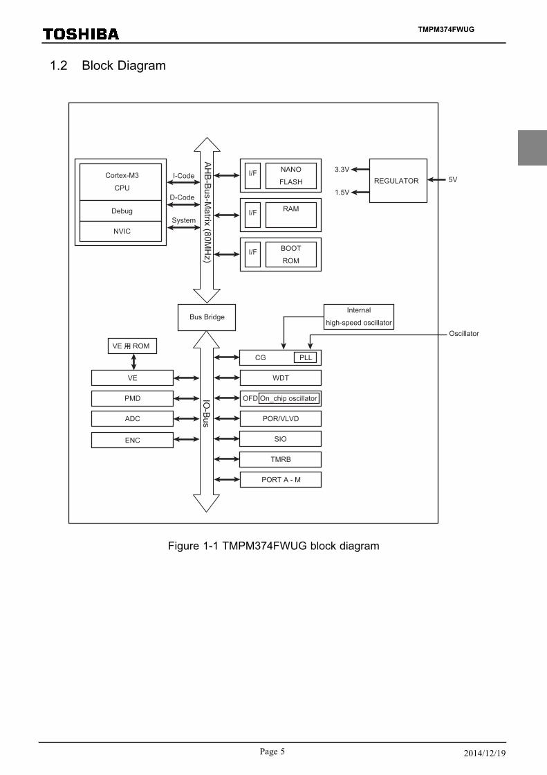
1.2 Block Diagram
I-Code
AH
B-B
us-Matrix (80M
Hz)
D-Code
System
Cortex-M3
CPU
Debug
NVIC
Bus Bridge
I/F NANO
FLASH
I/F RAM
I/F BOOT
ROM
REGULATOR3.3V
1.5V
5V
CG PLL
WDT
OFD On_chip oscillator
POR/VLVD
SIO
TMRB
PORT A - M
VE
PMD
ADC
ENC
VE ROMIO
-Bus
Oscillator
Internal
high-speed oscillator
Figure 1-1 TMPM374FWUG block diagram
TMPM374FWUG
Page 5 2014/12/19

1.3 Pin Layout (Top view)
The pin layout of TMPM374FWUG is a figure below.
Figure 1-2 Pin Layout (LQFP44)
TMPM374FWUG1.3 Pin Layout (Top view)
Page 62014/12/19
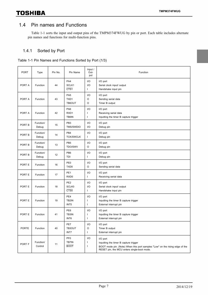
1.4 Pin names and FunctionsTable 1-1 sorts the input and output pins of the TMPM374FWUG by pin or port. Each table includes alternate
pin names and functions for multi-function pins.
1.4.1 Sorted by Port
Table 1-1 Pin Names and Functions Sorted by Port (1/3)
PORT Type Pin No. Pin NameInput /Out-put
Function
PORT A Function 44PA4SCLK1CTS1
I/OI/OI
I/O portSerial clock input/ outputHandshake input pin
PORT A Function 43PA5TXD1TB6OUT
I/OOO
I/O portSending serial dataTimer B output
PORT A Function 42PA6RXD1TB6IN
I/OII
I/O portReceiving serial dataInputting the timer B capture trigger
PORT BFunction/
Debug15
PB3TMS/SWDIO
I/OI/O
I/O portDebug pin
PORT BFunction/
Debug14
PB4TCK/SWCLK
I/OI
I/O portDebug pin
PORT BFunction/
Debug13
PB5TDO/SWV
I/OO
I/O portDebug pin
PORT BFunction/
Debug12
PB6TDI
I/OI
I/O portDebug pin
PORT E Function 16PE0TXD0
I/OO
I/O portSending serial data
PORT E Function 17PE1RXD0
I/OI
I/O portReceiving serial data
PORT E Function 18PE2SCLK0CTS0
I/OI/OI
I/O portSerial clock input/ outputHandshake input pin
PORT E Function 19PE4TB2ININT5
I/OII
I/O portInputting the timer B capture triggerExternal interrupt pin
PORT E Function 41PE6TB3ININT6
I/OII
I/O portInputting the timer B capture triggerExternal interrupt pin
PORTE Function 40PE7TB3OUTINT7
I/OOI
I/O portTimer B outputExternal interrupt pin
PORT FFunction/Control
11
PF0TB7INBOOT
I/OII
I/O portInputting the timer B capture triggerBOOT mode pin. (Note) When this port samples "Low" on the rising edge of theRESET pin, the MCU enters single-boot mode.
TMPM374FWUG
Page 7 2014/12/19

Table 1-1 Pin Names and Functions Sorted by Port (2/3)
PORT Type Pin No. Pin NameInput /Out-put
Function
PORT F Function 20
PF2ENCA1SCLK3CTS3
I/OII/OI
I/O portEncoder InputSerial clock input/ outputHandshake input pin
PORT F Function 21PF3ENCB1TXD3
I/OIO
I/O portEncoder InputSending serial data
PORT F Function 22PF4ENCZ1RXD3
I/OII
I/O portEncoder InputReceiving serial data
PORT G Function 1PG0UO1
I/OO
I/O portU-phase output pin
PORT G Function 2PG1XO1
I/OO
I/O portX-phase output pin
PORT G Function 3PG2VO1
I/OO
I/O portV-phase output pin
PORT G Function 4PG3YO1
I/OO
I/O portY-phase output pin
PORT G Function 5PG4WO1
I/OO
I/O portW-phase output pin
PORT G Function 6PG5ZO1
I/OO
I/O portZ-phase output pin
PORT G Function 7PG6EMG1
I/OI
I/O portEmergency status detection input
PORT G Function 8PG7OVV1
I/OI
I/O portOvervoltage Detection Input
PORT I Function 32PI3AINB2
I/OI
I/O portAnalog input
PORT J Function 33PJ0AINB3
I/OI
I/O portAnalog input
PORT J Function 34PJ6INTCAINB9
I/OII
I/O portExternal interrupt pinAnalog input
PORT J Function 35PJ7INTDAINB10
I/OII
I/O portExternal interrupt pinAnalog input
PORT K Function 36PK0INTEAINB11
I/OII
I/O portExternal interrupt pinAnalog input
PORT K Function 37PK1INTFAINB12
I/OII
I/O portExternal interrupt pinAnalog input
PORTM
Function/ Clock
24PM0X1
I/OI
I/O portConnected to a high-speed oscillator
TMPM374FWUG1.4 Pin names and Functions
Page 82014/12/19

Table 1-1 Pin Names and Functions Sorted by Port (3/3)
PORT Type Pin No. Pin NameInput /Out-put
Function
PORTM
Function/ Clock
26PM1X2
I/OO
I/O portConnected to a high-speed oscillator
- Control 28 MODE IMode pin(note) MODE pin must be connected to GND.
- Function 31 RESET IReset input pin(note) With a pull-up and a noise filter (about 30ns (typical value))
- PS 9 DVSS − GND pin
- PS 25 DVSS − GND pin
- PS 10 DVDD5 − Power supply pin
- PS 23 DVDD5 − Power supply pin
- PS 29 RVDD5 − Power supply pin
- PS 27 VOUT15 − Power supply pin
- PS 30 VOUT3 − Power supply pin
- PS 38AVSSBVREFLB
−AD converter: GND pin (Note 1)Supplying the AD converter with a reference power supply.
- PS 39AVDD5BVREFHB
−Supplying the AD converter with a power supply. (Note2)Supplying the AD converter with a reference power supply.
Note 1: AVSS must be connected to GND even if the AD converter is not used.Note 2: Must be connected to power supply even if AD converter is not used.
TMPM374FWUG
Page 9 2014/12/19
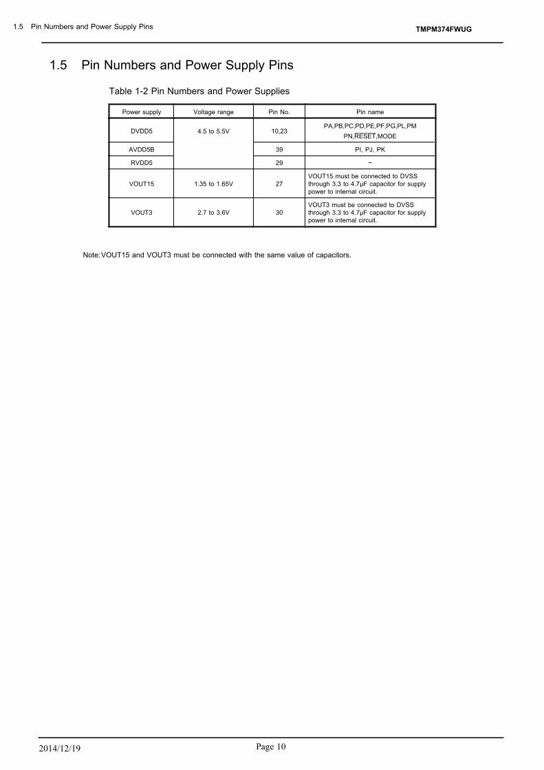
1.5 Pin Numbers and Power Supply Pins
Table 1-2 Pin Numbers and Power Supplies
Power supply Voltage range Pin No. Pin name
DVDD5 4.5 to 5.5V 10,23PA,PB,PC,PD,PE,PF,PG,PL,PM
PN,RESET,MODE
AVDD5B 39 PI, PJ, PK
RVDD5 29 −
VOUT15 1.35 to 1.65V 27VOUT15 must be connected to DVSSthrough 3.3 to 4.7μF capacitor for supplypower to internal circuit.
VOUT3 2.7 to 3.6V 30VOUT3 must be connected to DVSSthrough 3.3 to 4.7μF capacitor for supplypower to internal circuit.
Note:VOUT15 and VOUT3 must be connected with the same value of capacitors.
TMPM374FWUG1.5 Pin Numbers and Power Supply Pins
Page 102014/12/19

2. Processor Core
The TX03 series has a high-performance 32-bit processor core (the ARM Cortex-M3 processor core). For infor-mation on the operations of this processor core, please refer to the "Cortex-M3 Technical Reference Manual" is-sued by ARM Limited.This chapter describes the functions unique to the TX03 series that are not explained inthat document.
2.1 Information on the processor coreThe following table shows the revision of the processor core in the TMPM374FWUG.
Refer to the detailed information about the CPU core and architecture, refer to the ARM manual "Cortex-M ser-ies processors" in the following URL:
http://infocenter.arm.com/help/index.jsp
Product Name Core Revision
TMPM374FWUG r2p0
2.2 Configurable OptionsThe Cortex-M3 core has optional blocks. The optional blocks of the revision r2p0 are ETM™, MPU and WIC.
The following table shows the configurable options in the TMPM374FWUG.
Configurable Options Implementation
FPBTwo literal comparators
Six instruction comparators
DWT Four comparators
ITM Present
MPU Absent
ETM Present
AHB-AP Present
AHB Trace Macrocell In-terface Present
TPIU Present
WIC Absent
Debug Port JTAG / Serial wire
TMPM374FWUG
Page 11 2014/12/19

2.3 Exceptions/ InterruptionsExceptions and interruptions are described in the following section.
2.3.1 Number of Interrupt Inputs
The number of interrupt inputs can optionally be defined from 1 to 240 in the Cortex-M3 core.
TMPM374FWUG has 51 interrupt inputs. The number of interrupt inputs is reflected in <INTLINESNUM[4:0]> bit of NVIC register. In this product, if read <INTLINESNUM[4:0]> bit, 0x00 is read out.
2.3.2 Number of Priority Level Interrupt Bits
The Cortex-M3 core can optionally configure the number of priority level interrupt bits from 3 bits to 8 bits.
TMPM374FWUG has 3 priority level interrupt bits. The number of priority level interrupt bits is used for as-signing a priority level in the interrupt priority registers and system handler priority registers.
2.3.3 SysTick
The Cortex-M3 core has a SysTick timer which can generate SysTick exception.
For the detail of SysTick exception, refer to the section of "SysTick" in the exception and the register of Sy-sTick in the NVIC register.
2.3.4 SYSRESETREQ
The Cortex-M3 core outputs SYSRESETREQ signal when <SYSRESETREQ> bit of Application Inter-rupt and Reset Control Register are set.
TMPM374FWUG provides the same operation when SYSRESETREQ signal are output.
2.3.5 LOCKUP
When irreparable exception generates, the Cortex-M3 core outputs LOCKUP signal to show a serious er-ror included in software.
TMPM374FWUG does not use this signal. To return from LOCKUP status, it is necessary to use non-mask-able interruput (NMI) or reset.
2.3.6 Auxiliary Fault Status register
The Cortex-M3 core provides auxiliary fault status registers to supply additional system fault informationto software.
However, TMPM374FWUG is not defined this function. If auxiliary fault status register is read, always"0x0000_0000" is read out.
TMPM374FWUG
2. Processor Core
2.3 Exceptions/ Interruptions
Page 122014/12/19

2.4 EventsThe Cortex-M3 core has event output signals and event input signals. An event output signal is output by SEV in-
struction execution. If an event is input, the core returns from low-power consumption mode caused by WFE instruc-tion.
TMPM374FWUG does not use event output signals and event input signals. Please do not use SEV instructionand WFE instruction.
2.5 Power ManagementThe Cortex-M3 core provides power management system which uses SLEEPING signal and SLEEPDEEP sig-
nal. SLEEPDEEP signals are output when <SLEEPDEEP> bit of System Control Register is set.
These signals are output in the following circumstances:
-Wait-For-Interrupt (WFI) instruction execution
-Wait-For-Event (WFE) instruction execution
-the timing when interrupt-service-routine (ISR) exit in case that <SLEEPONEXIT> bit of System Control Reg-ister is set.
TMPM374FWUG does not use SLEEPDEEP signal so that <SLEEPDEEP> bit must not be set. And alsoevent signal is not used so that please do not use WFE instruction.
For detail of power management, refer to the Chapter "Clock/Mode control."
2.6 Exclusive accessIn Cortex-M3 core, the DCode bus system supports exclusive access. However TMPM374FWUG does not use
this function.
TMPM374FWUG
Page 13 2014/12/19

TMPM374FWUG
2. Processor Core
2.6 Exclusive access
Page 142014/12/19

3. Memory Map
3.1 Memory MapThe memory maps for TMPM374FWUG are based on the ARM Cortex-M3 processor core memory map. The in-
ternal ROM, internal RAM and special function registers (SFR) of TMPM374FWUG are mapped to the Code,SRAM and peripheral regions of the Cortex-M3 respectively. The special function register (SFR) means the con-trol registers of all input/output ports and peripheral functions. The SRAM and SFR areas are all included in thebit-band region.
The CPU register area is the processor core’s internal register region.
For more information on each region, see the "Cortex-M3 Technical Reference Manual".
Note that access to regions indicated as "Fault" causes a memory fault if memory faults are enabled, or causesa hard fault if memory faults are disabled. Also, do not access the vendor-specific region.
3.1.1 TMPM374FWUGMemory Map
Figure 3-1 shows the memory map of the TMPM374FWUG.
SFR
RAM (6K)
Internal ROM (128K)
Vendor-Specific
CPU Register Region
Fault
Fault
Fault
SFR
Fault
Figure 3-1 Memory Map
TMPM374FWUG
Page 15 2014/12/19

3.2 Details of SFR areaTable 3-1shows the details of the SFR area.
Do not access a reserved area in Table 3-1. See the chapter of each peripheral function for details.
Table 3-1 Details of SFR
Start Address End Address Peripheral
0x4000_0000 0x4000_033F PORT
0x4000_0340 0x4000_FFFF Reserved
0x4001_0000 0x4001_01FF TMRB
0x4001_0200 0x4001_04FF Reserved
0x4001_0500 0x4001_053F ENC
0x4001_0540 0x4002_007F Reserved
0x4002_0080 0x4002_017F SIO/UART
0x4002_0180 0x4003_01F Reserved
0x4003_0200 0x4003_02FF ADC
0x4003_0300 0x4003_FFFF Reserved
0x4004_0000 0x4004_003F WDT
0x4004_0040 0x4004_01FF Reserved
0x4004_0200 0x4004_023F CG
0x4004_0240 0x4004_02FF Reserved
0x4004_0300 0x4004_030F TRM
0x4004_0310 0x4004_07FF Reserved
0x4004_0800 0x4004_083F OFD
0x4004_0840 0x4004_08FF Reserved
0x4004_0900 0x4004_093F VLTD
0x4004_0940 0x4004_FFFF Reserved
0x4005_0000 0x4005_01FF VE
0x4005_0200 0x4005_047F Reserved
0x4005_0480 0x4005_04FF PMD
0x4005_0500 0x4007_FFFF Reserved
0x4008_0000 0x41FF_EFFF Hard fault
0x41FF_F000 0x41FF_F03F FLASH
0x41FF_F040 0x41FF_FFFF Reserved
TMPM374FWUG
3. Memory Map
3.2 Details of SFR area
Page 162014/12/19

4. Reset operation
4.1 Initial stateThe internal circuits, register settings and pin status are undefined right after the power-on. The state continues un-
til the RESET pin receives "Low" level signal after all the power supply voltage is applied.
4.2 Reset operationTMPM374FWUG has Power-on reset circuit, power-on reset signal is generated when power supply is turned
on. When reset from external RESET pin, input reset signal to RESET pin at "Low" level for minimum durationof 1.2μsec while power supply voltage is in the operating range.
4.3 After ResetWhen the reset is released, the system control register and the internal I/O register of the Cortex-M3 processor
core are initialized. Note that the PLL multiplication circuit stops after releasing the reset. Therefore, setCGOSCCR register and CGPLLSEL register to use PLL multiplication circuit.
After the reset exception handling is executed, the program branches off to the interrupt service routine. The ad-dress with which the interrupt service routine starts is stored in 0x0000_0004.
Note 1: It is possible to turn power on after RESET pin is set to "Low".Note 2: The reset operation may alter the internal RAM state.
TMPM374FWUG
Page 17 2014/12/19

TMPM374FWUG
4. Reset operation
4.3 After Reset
Page 182014/12/19

5. Clock / Mode Control
5.1 FeaturesThe clock/mode control block enables to select clock gear, prescaler clock and warm-up of the PLL clock multi-
plication circuit and oscillator.
There is also low power consumption mode which can reduce power consumption by mode transitions.
This chapter describes how to control clock operating modes and mode transitions.
The clock/mode control block has the following functions:
・ Controls the system clock・ Controls the prescaler clock・ Controls the PLL multiplication circuit・ Controls the warm-up timer
In addition to NORMAL mode, the TMPM374FWUG can operate in six types of low power mode to reduce pow-er consumption according to its usage conditions.
TMPM374FWUG
Page 19 2014/12/19

5.2 Registers
5.2.1 Register List
The following table shows the CG-related registers and addresses.
Base Address = 0x4004_0200
Register name Address (Base+)
System control register CGSYSCR 0x0000
Oscillation control register CGOSCCR 0x0004
Standby control register CGSTBYCR 0x0008
PLL selection register CGPLLSEL 0x000C
TMPM374FWUG
5. Clock / Mode Control
5.2 Registers
Page 202014/12/19

5.2.2 CGSYSCR (System control register)
31 30 29 28 27 26 25 24
bit symbol - - - - - - - -
After reset 0 0 0 0 0 0 0 0
23 22 21 20 19 18 17 16
bit symbol - - - - - - - -
After reset 0 0 0 0 0 0 0 1
15 14 13 12 11 10 9 8
bit symbol - - - FPSEL - PRCK
After reset 0 0 0 0 0 0 0 0
7 6 5 4 3 2 1 0
bit symbol - - - - - GEAR
After reset 0 0 0 0 0 0 0 0
Bit Bit Symbol Type Function
31-18 − R Read as "0".
17-16 − R/W Write as "01".
15-13 − R Read as "0".
12 FPSEL R/W Selects fperiph source clock0: fgear1: fc
11 − R Read as "0".
10- 8 PRCK[2:0] R/W Prescaler clock000: fperiph001: fperiph/2010: fperiph/4011: fperiph/8100: fperiph/16101: fperiph/32110: Reserved111: ReservedSpecifies the prescaler clock to peripheral I/O.
7-3 − R Read as "0".
2-0 GEAR[2:0] R/W High-speed clock (fc) gear000: fc001: Reserved010: Reserved011: Reserved100: fc/2101: fc/4110: fc/8111: fc/16
TMPM374FWUG
Page 21 2014/12/19

5.2.3 CGOSCCR (Oscillation control register)
31 30 29 28 27 26 25 24
bit symbol WUODR
After reset 1 0 0 0 0 0 0 0
23 22 21 20 19 18 17 16
bit symbol WUODR WUPSEL2 HOSCON OSCSEL XEN2
After reset 0 0 0 0 0 0 0 1
15 14 13 12 11 10 9 8
bit symbol - - - - - - - XEN1
After reset 0 0 0 0 0 0 0 0
7 6 5 4 3 2 1 0
bit symbol - - - - WUPSEL1 PLLON WUEF WUEON
After reset 0 0 0 0 0 0 0 0
Bit Bit Symbol Type Function
31-20 WUODR[11:0] R/W Specifies count time of the warm-up timer.
19 WUPSEL2 R/W Clock source for Warm-up timer(WUP)0: Internal (OSC2)1: External (OSC1)Select source clock for warm-up timer between external oscillator (OSC1) and internal oscillator (OSC2).
18 HOSCON R/W Port M or external oscillator (X1/X2) (Note1)0: PORT M1: External oscillator (X1/X2)Specifies Port M or X1/X2.When the external oscillator (OSC1) is used, Port M registers (PMCR/PMPUP/PMPDN/PMIE) should be dis-abled. After reset, the port M registers are disabled.
17 OSCSEL R/W Selection of high-speed oscillator0: Internal (OSC2)1: External (OSC1)Select high-speed oscillator between external oscillator (OSC1) and internal oscillator (OSC2). Confirm <OS-CSEL> become "1" then halt the OSC2 immediately after switching over to OSC1. Do not select OSC2again after switching to OSC1.
16 XEN2 R/W High-speed oscillator2 (Internal)0: Stop1:OscillationSpecifies operation of the high-speed oscillator 2 (OSC2).
15-12 − R/W Write as "0".
11-10 − R Read as "0".
9 − R/W Write as "0".
8 XEN1 R/W High-speed oscillator1 (External)0: Stop1:OscillationSpecifies operation of the high-speed oscillator 1 (OSC1).
7-4 − R/W Read as "0".
3 WUPSEL1 R/W Clock source for Warm-up timerWrite as "0".
2 PLLON R/W PLL operation0: Stop1: OscillationSpecifies operation of the PLL.It stops after reset.Setting the bit is required.
TMPM374FWUG
5. Clock / Mode Control
5.2 Registers
Page 222014/12/19

Bit Bit Symbol Type Function
1 WUEF R Status of warm-up timer (WUP) (Note2)0: Warm-up completed.1: Warm-up operationEnable to monitor the status of the warm-up timer.
0 WUEON W Operation of warm-up timer (Note2)0: don't care1: Starting warm-upEnables to start the warm-up timer.
Note 1: When the <HOSCON> is set to "1", the all registers for Port M can not be accessed and the read data fromthese registers are always "0". If one of the Port M registers except PMDATA and PMOD is not equal to the ini-tial value, the <HOSCON> can not be set to "1".
Note 2: Do not write "1" to <WUEON>, at the setting of returning from stop mode with automatic warming-up. When warm-ing-up is started by software (<WUOEN> = "1" ), please monitor <WUEF> and confirm warming-up is comple-ted. After <WUEN> turn to "0" operation mode can be changed to stop mode.
TMPM374FWUG
Page 23 2014/12/19

5.2.4 CGSTBYCR (Standby control register)
31 30 29 28 27 26 25 24
bit symbol - - - - - - - -
After reset 0 0 0 0 0 0 0 0
23 22 21 20 19 18 17 16
bit symbol - - - - - - - DRVE
After reset 0 0 0 0 0 0 0 0
15 14 13 12 11 10 9 8
bit symbol - - - - - - - RXEN
After reset 0 0 0 0 0 0 0 1
7 6 5 4 3 2 1 0
bit symbol - - - - - STBY
After reset 0 0 0 0 0 0 1 1
Bit Bit Symbol Type Function
31-18 − R Read as "0".
17 − R/W Write as "0".
16 DRVE R/W Pin status in STOP mode0: Inactive1: Active
15-10 − R Read as "0".
9 − R/W Write as "0".
8 RXEN R/W High-speed oscillator operation after releasing STOP mode. Write as "1".
7-3 − R Read as "0".
2-0 STBY[2:0] R/W Low power consumption mode000: Reserved001: STOP010: Reserved011: IDLE100: Reserved101: Reserved110: Reserved111: Reserved To enter STOP mode, disable the oscillation (OSC1 or OSC2) which is unused as system clock.
TMPM374FWUG
5. Clock / Mode Control
5.2 Registers
Page 242014/12/19

5.2.5 CGPLLSEL (PLL Selection Register)
31 30 29 28 27 26 25 24
bit symbol - - - - - - - -
After reset 0 0 0 0 0 0 0 0
23 22 21 20 19 18 17 16
bit symbol - - - - - - - -
After reset 0 0 0 0 0 0 0 0
15 14 13 12 11 10 9 8
bit symbol - - - - - - - -
After reset 1 0 1 0 0 0 0 1
7 6 5 4 3 2 1 0
bit symbol - - - - - - - PLLSEL
After reset 0 0 1 1 1 1 1 0
Bit Bit Symbol Type Function
31-16 − R Read as "0".
15-12 − R/W Write as "1010".
11 − R Read as "0".
10-1 − R/W Write as "00_1001_1111".
0 PLLSEL R/W Use of PLL0: fosc use1: PLL UseSpecifies use or disuse of the clock multiplied by the PLL."fosc" is automatically set after reset. Resetting is required when using the PLL.
Note 1: Be sure to disable OFD when enabling PLL. Especially, be careful setting PLL in the initial routine because OFDis available after OFD reset.Example :OFDCR1<OFDWEN7:0>= "0xF9" : Sets control register write enable codeOFDCR2<OFDEN7:0>= "0x00" : Disable OFDCGPLLSEL<PLLSEL>= "1" : Enable PLLOFDMNPLLON= "xxxx" : Sets lower detection frequencyOFDMXPLLON= "yyyy" : Sets higher detection frequencyOFDCR2<OFDEN7:0>= "0xE4" : Enable OFDOFDCR1<OFDWEN7:0>= "0x06" : Sets control register write disable code
Note 2: The maximum operating frequency is 32 MHz when using within the range from 85 to 100 °C. Be careful not to ex-ceed the maximum operating frequency by dividing system clock when using PLL.
TMPM374FWUG
Page 25 2014/12/19
5.3 Clock control
5.3.1 Clock Type
Each clock is defined as follows :
fosc1 : Clock input from external high-speed oscillator (X1 and X2)
fosc2 : Clock input from internal high-speed oscillator
fosc : High-speed clock specified by CGOSCCR<OSCSEL>
fPLL : Clock octupled by PLL (x 8)
fc : Clock specified by CGPLLSEL<PLLSEL> (high-speed clock)
fgear : Clock specified by CGSYSCR<GEAR[2:0]>
fsys : The same clock as fgear (system clock)
fperiph : Clock specified by CGSYSCR<FPSEL>
φT0 : Clock specified by CGSYSCR<PRCK[2:0]> (Prescaler clock)
The high-speed clock fc and the prescaler clock φT0 are dividable as follows.
High-speed clock : fc, fc/2, fc/4, fc/8, fc/16
Prescaler clock : fperiph, fperiph/2, fperiph/4, fperiph/8, fperiph/16, fperiph/32
5.3.2 Initial Values after Reset
Reset operation initializes the clock configuration as follows.
External high-speed oscillator (OSC1) : Stop (X1,X2)
Internal high-speed oscillator (OSC2) : Oscillating
PLL (Phase locked loop circuit) : Stop
High-speed clock gear : fc (no frequency dividing)
Reset operation causes all the clock configurations to be the same as fOSC2.
fC = fOSC2
fSYS = fC ( = fOSC2 )
fperiph = fC ( = fOSC2 )
φT0 = fperiph ( = fOSC2 )
TMPM374FWUG
5. Clock / Mode Control
5.3 Clock control
Page 262014/12/19

5.3.3 Clock system Diagram
Figure 5-1 shows the clock system diagram.
Warm-up timer
CGOSCCR<WUEON>CGOSCCR<WUODR[11:0]>
Internaloscillator
PLL
AD conversion clockOFD monitoring clock
CGSYSCR<FPSEL>
fgear
fperiph(to Peripheral I/O)
fsys
CGPLLSEL<PLLSEL>
CGOSCCR<WUPSEL2>
Externaloscillator
CGOSCCR<XEN2>
Starts oscillation after reset
fosc2
CGOSCCR<PLLON>Stops after releasing reset
CGOSCCR<XEN1>
Stops oscillation after reset
fPLL= fOSC×8
fcCGSYSCR
<GEAR[2:0]>
Peripheral I/O prescaler input TMRB, SIO, SBI
1/321/161/8
CGSYSCR<PRCK[2:0]>
1/41/2fperiph
T0
SysTick external refference clock CPU
AHB-Bus I/O CPU, ROM, RAM, BOOT ROM
IO-Bus I/O TMRB, WDT, VE, PMD, SIO, ADC, PORT, OFD, ENC, VLTD
fosc1
fosc1/81/41/2 1/16
CGOSCCR<OSCSEL>
1/32
X2
X1
TMRB, SIO
Figure 5-1 Clock Block Diagram
The input clocks selector shown with an arrow are set as default after reset.
TMPM374FWUG
Page 27 2014/12/19
5.3.4 Clock Multiplication Circuit (PLL)
This circuit outputs the fPLL clock that is octuple of the high-speed oscillator output clock (fosc.) As a re-sult, the input frequency to oscillator can be low, and the internal clock be made high-speed.
The PLL is disabled after reset. To enable the PLL, set "1" to the CGOSCCR<PLLON> bit and set "1" tothe CGPLLSEL<PLLSEL>. Then fPLL clock output is octuple of the high-speed oscillator (fosc).
The PLL requires a certain amount of time to be stabilized, which should be secured using the warm-up func-tionor other methods.
Note:When the PLL starts operation, it is necessary to wait at least 200μs for stabilization of the PLL.
TMPM374FWUG
5. Clock / Mode Control
5.3 Clock control
Page 282014/12/19
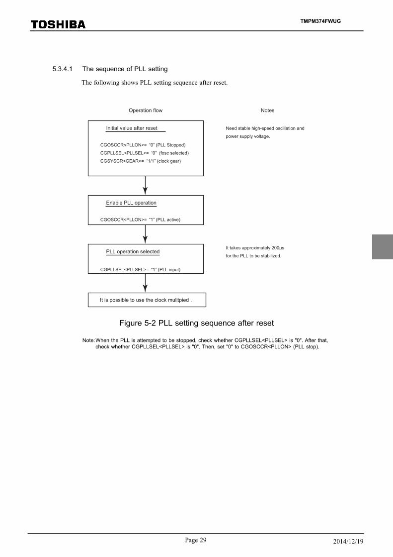
5.3.4.1 The sequence of PLL setting
The following shows PLL setting sequence after reset.
Initial value after reset
CGOSCCR<PLLON>= “0” (PLL Stopped)
CGPLLSEL<PLLSEL>= “0” (fosc selected)
CGSYSCR<GEAR>= “1/1” (clock gear)
Need stable high-speed oscillation and
power supply voltage.
Operation flow Notes
It is possible to use the clock mulitpied .
Enable PLL operation
CGOSCCR<PLLON>= “1” (PLL active)
PLL operation selected
CGPLLSEL<PLLSEL>= “1” (PLL input)
It takes approximately 200μs
for the PLL to be stabilized.
Figure 5-2 PLL setting sequence after reset
Note:When the PLL is attempted to be stopped, check whether CGPLLSEL<PLLSEL> is "0". After that,check whether CGPLLSEL<PLLSEL> is "0". Then, set "0" to CGOSCCR<PLLON> (PLL stop).
TMPM374FWUG
Page 29 2014/12/19

5.3.5 Warm-up function
The warm-up function secures the stability time for the oscillator and the PLL with the warm-up timer.The warm-up function is used when returning from STOP mode. For detail function, describes in "5.6.6 Warm-up".
Note:Do not shift to STOP mode, during operating warm-up timer.
In this case, an interrupt for returning from low power consumption mode triggers the automatic timercount. After the specified time is reached, the system clock is output and the CPU starts operation.
How to configure the warm-up function.
1. Specify the count up clock
Specify the count up clock for the warm-up counter in the CGOSCCR<WUPSEL1> and <WU-PSEL2> bit. (Write "0" to <WUPSEL1> and write "0" or "1" to <WUPSEL2>. "0" specifies inter-nal oscillator and "1" specifies external oscillator.)
2. Specify the warm-up counter value
The warm-up time can be selected by setting the CGOSCCR<WUODR[11:0]>.
The following shows the warm-up setting and example.
Warm-up cycles = Setting value of warm-up time
Input cycle by frequency(s)
<example 1>Setting 5 ms of warm-up time with 8MHz oscillator
Setting value of warm-up time
Input cycle by frequency(s)=
5ms
1/8MHz = 40,000 0x9C40
Drop the last 4 bits, set 0x9C4 into the CGOSCCR<WUODR[11:0]>.
3. Confirm the start and completion of warm-up
The CGOSCCR<WUEON><WUEF> is used to confirm the start and completion of warm-upthrough software (instruction).
Note: The warm-up timer operates according to the oscillation clock, and it may contain errors if there is any fluctua-tion in the oscillation frequency. Therefore, the warm-up time should be taken as approximate time.
TMPM374FWUG
5. Clock / Mode Control
5.3 Clock control
Page 302014/12/19
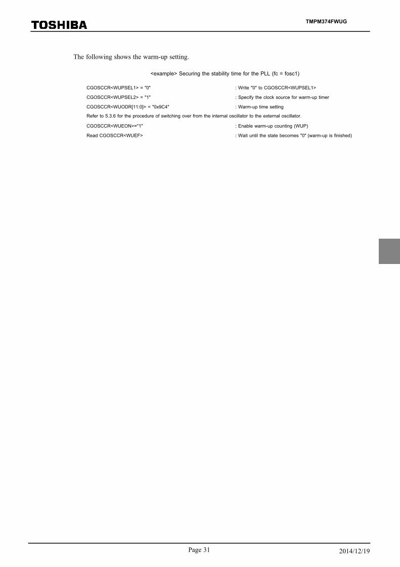
The following shows the warm-up setting.
<example> Securing the stability time for the PLL (fc = fosc1)
CGOSCCR<WUPSEL1> = "0" : Write "0" to CGOSCCR<WUPSEL1>
CGOSCCR<WUPSEL2> = "1" : Specify the clock source for warm-up timer
CGOSCCR<WUODR[11:0]> = "0x9C4" : Warm-up time setting
Refer to 5.3.6 for the procedure of switching over from the internal oscillator to the external oscillator.
CGOSCCR<WUEON>="1" : Enable warm-up counting (WUP)
Read CGOSCCR<WUEF> : Wait until the state becomes "0" (warm-up is finished)
TMPM374FWUG
Page 31 2014/12/19
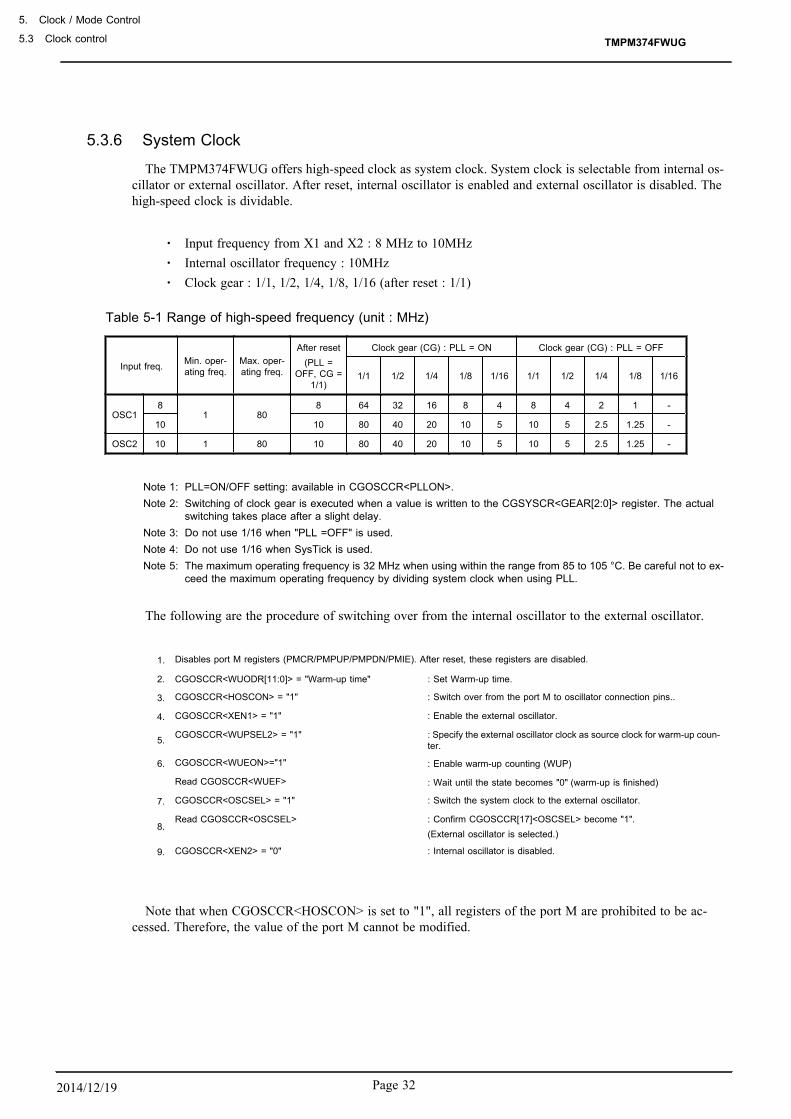
5.3.6 System Clock
The TMPM374FWUG offers high-speed clock as system clock. System clock is selectable from internal os-cillator or external oscillator. After reset, internal oscillator is enabled and external oscillator is disabled. Thehigh-speed clock is dividable.
・ Input frequency from X1 and X2 : 8 MHz to 10MHz・ Internal oscillator frequency : 10MHz・ Clock gear : 1/1, 1/2, 1/4, 1/8, 1/16 (after reset : 1/1)
Table 5-1 Range of high-speed frequency (unit : MHz)
Input freq. Min. oper-ating freq.
Max. oper-ating freq.
After reset(PLL =
OFF, CG =1/1)
Clock gear (CG) : PLL = ON Clock gear (CG) : PLL = OFF
1/1 1/2 1/4 1/8 1/16 1/1 1/2 1/4 1/8 1/16
OSC18
1 808 64 32 16 8 4 8 4 2 1 -
10 10 80 40 20 10 5 10 5 2.5 1.25 -
OSC2 10 1 80 10 80 40 20 10 5 10 5 2.5 1.25 -
Note 1: PLL=ON/OFF setting: available in CGOSCCR<PLLON>.Note 2: Switching of clock gear is executed when a value is written to the CGSYSCR<GEAR[2:0]> register. The actual
switching takes place after a slight delay.Note 3: Do not use 1/16 when "PLL =OFF" is used.Note 4: Do not use 1/16 when SysTick is used.Note 5: The maximum operating frequency is 32 MHz when using within the range from 85 to 105 °C. Be careful not to ex-
ceed the maximum operating frequency by dividing system clock when using PLL.
The following are the procedure of switching over from the internal oscillator to the external oscillator.
1. Disables port M registers (PMCR/PMPUP/PMPDN/PMIE). After reset, these registers are disabled.
2. CGOSCCR<WUODR[11:0]> = "Warm-up time" : Set Warm-up time.
3. CGOSCCR<HOSCON> = "1" : Switch over from the port M to oscillator connection pins..
4. CGOSCCR<XEN1> = "1" : Enable the external oscillator.
5. CGOSCCR<WUPSEL2> = "1" : Specify the external oscillator clock as source clock for warm-up coun-ter.
6. CGOSCCR<WUEON>="1" : Enable warm-up counting (WUP)
Read CGOSCCR<WUEF> : Wait until the state becomes "0" (warm-up is finished)
7. CGOSCCR<OSCSEL> = "1" : Switch the system clock to the external oscillator.
8.Read CGOSCCR<OSCSEL> : Confirm CGOSCCR[17]<OSCSEL> become "1".
(External oscillator is selected.)
9. CGOSCCR<XEN2> = "0" : Internal oscillator is disabled.
Note that when CGOSCCR<HOSCON> is set to "1", all registers of the port M are prohibited to be ac-cessed. Therefore, the value of the port M cannot be modified.
TMPM374FWUG
5. Clock / Mode Control
5.3 Clock control
Page 322014/12/19
5.3.7 Prescaler Clock Control
Each peripheral function has a prescaler for dividing a clock. As the clock φT0 to be input to each prescal-er, the "fperiph" clock specified in the CGSYSCR<FPSEL> can be divided according to the setting in theCGSYSCR<PRCK[2:0]>. After the controller is reset, fperiph/1 is selected as φT0.
Note:When the clock gear is used, specify the time for the prescaler output Tn, which is from each periph-eral function, to be slower than fsys ( Tn < fsys). Do not switch the clock gear while the timer coun-ter or other peripheral functions are operating.
TMPM374FWUG
Page 33 2014/12/19

5.4 Modes and Mode Transitions
5.4.1 Mode Transitions
NORMAL mode use the high-speed clock for the system clock .
IDLE and STOP modes can be used as low power consumption mode that enables to reduce power consump-tion by halting processor core operation.
Figure 5-3 shows mode transition diagram.
For a detail of sleep-on-exit, refer to "Cortex-M3 Technical Reference Manual".
Reset has been performed.
Interrupt(Note)
NORMAL mode
Reset
IDLE mode(Stops CPU)
(Selectable IO Operation)
STOP mode(Halts all circuit)
Instruction/sleep on exit
Instruction/sleep on exit
Interrupt(Note)
Figure 5-3 Mode Transition Diagram
Note:The warm-up is needed. The warm-up time must be set in NORMAL mode before changing toSTOP mode. Regarding warm-up time, refer to "5.6.6 Warm-up".
TMPM374FWUG
5. Clock / Mode Control
5.4 Modes and Mode Transitions
Page 342014/12/19

5.5 Operation ModeAs an operation mode, NORMAL is available. The features of NORMAL mode are described in the following sec-
tion.
5.5.1 NORMAL mode
This mode is to operate the CPU core and the peripheral hardware by using the high-speed clock.
It is shifted to NORMAL mode after reset.
TMPM374FWUG
Page 35 2014/12/19
5.6 Low Power Consumption ModesThe TMPM374FWUG has two low power consumption modes: IDLE and STOP. To shift to low power consump-
tion mode, specify the mode in the system control register CGSTBYCR<STBY[2:0]> and execute the WFI (WaitFor Interrupt) instruction.In this case, execute reset or generate the interrupt to release the mode. Releasing by theinterrupt requires settings in advance. See the chapter "Exceptions" for details.
Note 1: The TMPM374FWUG does not offer any event for releasing low power consumption mode. Transition to lowpower consumption mode by executing the WFE (Wait For Event) instruction is prohibited.
Note 2: The TMPM374FWUG does not support low power consumption mode configured with the SLEEPDEEP bit inthe Cortex-M3 core. Setting the <SLEEPDEEP> bit of the system control register is prohibited.
The features of each mode are described as follows.
5.6.1 IDLE Mode
Only the CPU is stopped in this mode. Each peripheral function has one bit in its control register for ena-bling or disabling operation in IDLE mode. When IDLE mode is entered, peripheral functions for which oper-ation in IDLE mode is disabled stop operation and hold the state at that time.
The following peripheral functions can be enabled or disabled in IDLE mode. For setting details, see the chap-ter on each peripheral function.
・ 16-bit timer / event counter (TMRB)・ Serial channel (SIO/UART)・ Watchdog timer (WDT)・ Vector Engine (VE)
Note:WDT should be stopped before entering IDLE mode.
TMPM374FWUG
5. Clock / Mode Control
5.6 Low Power Consumption Modes
Page 362014/12/19

5.6.2 STOP mode
All the internal circuits including the internal oscillator are brought to a stop in STOP mode.
By releasing STOP mode, the device returns to the preceding mode of STOP mode and starts operation.
STOP mode enables to select the pin status by setting the CGSTBYCR<DRVE>. Table 5-2 shows the pin sta-tus in STOP mode.
Table 5-2 Pin States in STOP mode
Pin name I/O <DRVE> = 0 <DRVE> = 1
Notport
RESET, MODE Input only ο
VOUT15, VOUT3 Output only ο
Port
X1 Input only ×
X2 Output only "High" level output
TMSTCKTDI
Input ο
TDO/SWV OutputEnabled when data is valid.
Disabled when data is invalid.
SWCLK Input ο
SWDIO
Input ο
OutputEnabled when data is valid.
Disabled when data is invalid.
UO1, VO1, WO1, XO1,YO1, ZO1 Output × ο
INT5, INT6, INT7INTC, INTD, INTEINTF
Input ο
Other function pins otherthan the above or theports that are used as gen-eral purpose ports.
Input × ο
Output × ο
ο : Input or output enabled.× : Input or output disabled.
TMPM374FWUG
Page 37 2014/12/19

5.6.3 Low power Consumption Mode Setting
Low power consumption mode is specified by the setting of the standby control register CGSTBYCR<STBY[2:0]>.
Table 5-3 shows the mode setting in the <STBY[2:0]>.
Table 5-3 Low power consumption mode setting
ModeCGSTBYCR<STBY[2:0]>
STOP 001
IDLE 011
Note:Do not set any value other than those shown above in <STBY[2:0]>.
5.6.4 Operational Status in Each Mode
Table 5-4 shows the operational status in each mode.
Table 5-4 Operational Status in Each Mode
Block NORMAL IDLE STOP
Processor core ο × ×
I/O port ο ο * (Note1)
PMD ο ο ×
ENC ο ο ×
OFD ο ο ×
ADC ο ο ×
VE ο
ON/OFF se-lectable for
each module
×
SIO ο ×
TMRB ο ×
WDT ο ×
VLTD ο ο ο (Note2)
POR ο ο ο (Note2)
CG ο ο ×
PLL ο ο ×
High-speed oscilla-tor (fc) ο ο ×
ο : Operating
× : Stopped
Note 1: It depends on CGSTBYCR<DRVE>.Note 2: The blocks are not stopped even though the clock is halted.
TMPM374FWUG
5. Clock / Mode Control
5.6 Low Power Consumption Modes
Page 382014/12/19
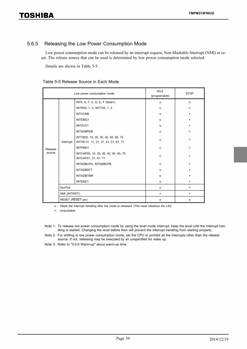
5.6.5 Releasing the Low Power Consumption Mode
Low power consumption mode can be released by an interrupt request, Non-Maskable Interrupt (NMI) or re-set. The release source that can be used is determined by low power consumption mode selected.
Details are shown in Table 5-5.
Table 5-5 Release Source in Each Mode
Low power consumption modeIDLE
(programable)STOP
Releasesource
Interrupt
INT5, 6, 7, C, D, E, F (Note1) ο ο
INTRX0, 1, 3, INTTX0, 1, 3 ο ×
INTVCNB ο ×
INTEMG1 ο ×
INTOVV1 ο ×
INTADBPDB ο ×
INTTB00, 10, 20, 30, 40, 50, 60, 70INTTB 01, 11, 21, 31, 41, 51, 61, 71
ο ×
INTPMD1 ο ×
INTCAP00, 10, 20, 30, 40, 50, 60, 70INTCAP21, 31, 61, 71
ο ×
INTADBCPA, INTADBCPB ο ×
INTADBSFT ο ×
INTADBTMR ο ×
INTENC1 ο ×
SysTick ο ×
NMI (INTWDT) × ×
RESET (RESET pin) ο ο
ο :× :
Starts the interrupt handling after the mode is released. (The reset initializes the LSI)Unavailable
Note 1: To release low power consumption mode by using the level mode interrupt, keep the level until the interrupt han-dling is started. Changing the level before then will prevent the interrupt handling from starting properly.
Note 2: For shifting to low power consumption mode, set the CPU to prohibit all the interrupts other than the releasesource. If not, releasing may be executed by an unspecified for wake up.
Note 3: Refer to "5.6.6 Warm-up" about warm-up time.
TMPM374FWUG
Page 39 2014/12/19

・ Release by interrupt request
To release low power consumption mode by an interrupt, the CPU must be set in advance to de-tect the interrupt. In addition to the setting in the CPU, the clock generator must be set to detectthe interrupt to be used to release STOP modes.
・ Release by Non-Maskable Interrupt (NMI)
There is a watchdog timer interrupt (INTWDT) as a non-maskable interrupt source. INTWDTcan only be used in IDLE mode.
Note: Note that the WDT cannot be cleared by the CPU operation in IDLE mode.
・ Release by reset
All low power consumption modes can be released by reset from the RESET pin. After that, themode switches to NORMAL mode and all the registers are initialized as is the case with normal reset.
・ Release by SysTick interrupt
SysTick interrupt can only be used in IDLE mode.
Refer to "Interrupts" for detail.
TMPM374FWUG
5. Clock / Mode Control
5.6 Low Power Consumption Modes
Page 402014/12/19

5.6.6 Warm-up
Mode transition may require the warm-up so that the internal oscillator provides stable oscillation.
In the mode transition from STOP to the NORMAL, the warm-up counter is activated automatically. Andthen the system clock output is started after the elapse of configured warm-up time. It is necessary to set a os-cillator to be used for warm-up in the CGOSCCR<WUPSEL1><WUPSEL2> (Note1) and to set a warm-uptime in the CGOSCCR<WUODR> before executing the instruction to enter STOP mode.
Note 1: Always set CGOSCCR<WUPSEL1> to "0".Note 2: In STOP modes, the PLL is disabled. When returning from these modes, configure the warm-up time in con-
sideration of the stability time of the PLL and the internal oscillator. It takes approximately 200μs for thePLL to be stabilized.
Note 3: Do not write "1" to CGOSCCR<WUEON> bit, at the setting of returning from low consumption modewith automatic warming-up.
Table 5-6 shows whether the warm-up setting of each mode transition is required or not.
Table 5-6 Warm-up setting in mode transition
Mode transition Warm-up setting
NORMAL → IDLE Not required
NORMAL → STOP Not required
IDLE → NORMAL Not required
STOP → NORMAL Auto-warm-up
TMPM374FWUG
Page 41 2014/12/19

5.6.7 Clock Operation in Mode Transition
The clock operation in mode transition are described Chapter 5.6.7.1.
5.6.7.1 Transition of operation modes : NORMAL → STOP → NORMAL
When returning to NORMAL mode from STOP mode, the warm-up is activated automatically. It is nec-essary to set the warm-up time before entering STOP mode.
Returning to NORMAL mode by reset does not induce the automatic warm-up. Keep the reset signal as-serted until the oscillator operation becomes stable.
fsys(System clock)
STOP
fosc
NORMALNORMALMode
Warm-up
System clock stops High-speed clock starts oscillatingWarm-up starts
WFI execute/sleep on exit Release event occurs
Warm-up completes.System clock starts.
TMPM374FWUG
5. Clock / Mode Control
5.6 Low Power Consumption Modes
Page 422014/12/19

6. Exceptions
This chapter describes features, types and handling of exceptions.
Exceptions have close relation to the CPU core. Refer to "Cortex-M3 Technical Reference Manual" if needed.
6.1 OverviewExceptions have close relation to the CPU core. Refer to "Cortex-M3 Technical Reference Manual" if needed.
There are two types of exceptions: those that are generated when some error condition occurs or when an instruc-tion to generate an exception is executed; and those that are generated by hardware, such as an interrupt request sig-nal from an external pin or peripheral function.
All exceptions are handled by the Nested Vectored Interrupt Controller (NVIC) in the CPU according to the re-spective priority levels. When an exception occurs, the CPU stores the current state to the stack and branches tothe corresponding interrupt service routine (ISR). Upon completion of the ISR, the information stored to the stackis automatically restored.
6.1.1 Exception types
The following types of exceptions exist in the Cortex-M3.
For detailed descriptions on each exception, refer to "Cortex-M3 Technical Reference Manual".
・ Reset・ Non-Maskable Interrupt (NMI)・ Hard Fault・ Memory Management・ Bus Fault・ Usage Fault・ SVCall (Supervisor Call)・ Debug Monitor・ PendSV・ SysTick・ External Interrupt
TMPM374FWUG
Page 43 2014/12/19

6.1.2 Handling Flowchart
The following shows how an exception/interrupt is handled. In the following descriptions, indicates hardware handling. indicates software handling.
Each step is described later in this chapter.
Processing Description See
Detection by CG/CPU The CG/CPU detects the exception request. Section 6.1.2.1
Handling by CPU The CPU handles the exception request.
Section 6.1.2.2
Branch to ISR The CPU branches to the corresponding interrupt service routine (ISR).
Execution of ISR Necessary processing is executed. Section 6.1.2.4
Return from exception The CPU branches to another ISR or returns to the previous program. Section 6.1.2.4
TMPM374FWUG
6. Exceptions
6.1 Overview
Page 442014/12/19

6.1.2.1 Exception Request and Detection
(1) Exception occurrence
Exception sources include instruction execution by the CPU, memory accesses, and interrupt re-quests from external interrupt pins or peripheral functions.
An exception occurs when the CPU executes an instruction that causes an exception or when an er-ror condition occurs during instruction execution.
An exception also occurs by an instruction fetch from the Execute Never (XN) region or an ac-cess violation to the Fault region.
An interrupt request is generated from an external interrupt pin or peripheral function.For inter-rupts that are used for releasing a standby mode, relevant settings must be made in the clock genera-tor. For details, refer to "6.5 Interrupts".
(2) Exception detection
If multiple exceptions occur simultaneously, the CPU takes the exception with the highest priority.
Table 6-1 shows the priority of exceptions. "Configurable" means that you can assign a priority lev-el to that exception. Memory Management, Bus Fault and Usage Fault exceptions can be enabled ordisabled. If a disabled exception occurs, it is handled as Hard Fault.
Table 6-1 Exception Types and Priority
No. Exception type Priority Description
1 Reset −3 (highest) Reset pin, WDT, POR, VLTD, OFD or SYSRETREQ
2 Non-Maskable Interrupt −2 WDT
3 Hard Fault −1 Fault that cannot activate because a higher-priority fault is being han-dled or it is disabled
4 Memory Management ConfigurableException from the Memory Protection Unit (MPU) (Note 1)Instruction fetch from the Execute Never (XN) region
5 Bus Fault Configurable Access violation to the Hard Fault region of the memory map
6 Usage Fault Configurable Undefined instruction execution or other faults related to instruction ex-ecution
7~10 Reserved −
11 SVCall Configurable System service call with SVC instruction
12 Debug Monitor Configurable Debug monitor when the CPU is not faulting
13 Reserved −
14 PendSV Configurable Pendable system service request
15 SysTick Configurable Notification from system timer
16~ External interrupt Configurable External interrupt pin or peripheral function (Note2)
Note 1: This product does not contain the MPU.Note 2: External interrupts have different sources and numbers in each product. For details,
see"6.5.1.5 List of Interrupt Sources".
TMPM374FWUG
Page 45 2014/12/19
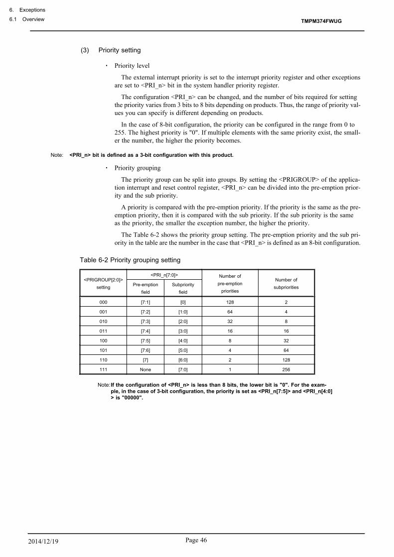
(3) Priority setting
・ Priority level
The external interrupt priority is set to the interrupt priority register and other exceptionsare set to <PRI_n> bit in the system handler priority register.
The configuration <PRI_n> can be changed, and the number of bits required for settingthe priority varies from 3 bits to 8 bits depending on products. Thus, the range of priority val-ues you can specify is different depending on products.
In the case of 8-bit configuration, the priority can be configured in the range from 0 to255. The highest priority is "0". If multiple elements with the same priority exist, the small-er the number, the higher the priority becomes.
Note: <PRI_n> bit is defined as a 3-bit configuration with this product.
・ Priority grouping
The priority group can be split into groups. By setting the <PRIGROUP> of the applica-tion interrupt and reset control register, <PRI_n> can be divided into the pre-emption prior-ity and the sub priority.
A priority is compared with the pre-emption priority. If the priority is the same as the pre-emption priority, then it is compared with the sub priority. If the sub priority is the sameas the priority, the smaller the exception number, the higher the priority.
The Table 6-2 shows the priority group setting. The pre-emption priority and the sub pri-ority in the table are the number in the case that <PRI_n> is defined as an 8-bit configuration.
Table 6-2 Priority grouping setting
<PRIGROUP[2:0]>setting
<PRI_n[7:0]> Number ofpre-emption
priorities
Number ofsubprioritiesPre-emption
fieldSubpriority
field
000 [7:1] [0] 128 2
001 [7:2] [1:0] 64 4
010 [7:3] [2:0] 32 8
011 [7:4] [3:0] 16 16
100 [7:5] [4:0] 8 32
101 [7:6] [5:0] 4 64
110 [7] [6:0] 2 128
111 None [7:0] 1 256
Note: If the configuration of <PRI_n> is less than 8 bits, the lower bit is "0". For the exam-ple, in the case of 3-bit configuration, the priority is set as <PRI_n[7:5]> and <PRI_n[4:0]> is "00000".
TMPM374FWUG
6. Exceptions
6.1 Overview
Page 462014/12/19

6.1.2.2 Exception Handling and Branch to the Interrupt Service Routine (Pre-emption)
When an exception occurs, the CPU suspends the currently executing process and branches to the inter-rupt service routine. This is called "pre-emption".
(1) Stacking
When the CPU detects an exception, it pushes the contents of the following eight registers to thestack in the following order :
・ Program Counter (PC)・ Program Status Register (xPSR)・ r0 to r3・ r12・ Link Register (LR)
The SP is decremented by eight words by the completion of the stack push.The following showsthe state of the stack after the register contents have been pushed.
Old SP → <previous>
xPSR
PC
LR
r12
r3
r2
r1
SP → r0
(2) fetching an ISR
The CPU enables instruction to fetch the interrupt processing with data store to the register.
Prepare a vector table containing the top addresses of ISRs for each exception.After reset, the vec-tor table is located at address 0x0000_0000 in the Code area.By setting the Vector Table Offset Reg-ister, you can place the vector table at any address in the Code or SRAM space.
The vector table should also contain the initial value of the main stack.
(3) Late-arriving
If the CPU detects a higher priority exception before executing the ISR for a previous exception,the CPU handles the higher priority exception first. This is called "late-arriving".
A late-arriving exception causes the CPU to fetch a new vector address for branching to the corre-sponding ISR, but the CPU does not newly push the register contents to the stack.
(4) Vector table
The vector table is configured as shown below.
TMPM374FWUG
Page 47 2014/12/19
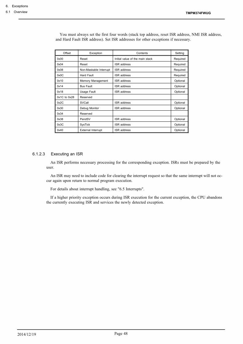
You must always set the first four words (stack top address, reset ISR address, NMI ISR address,and Hard Fault ISR address). Set ISR addresses for other exceptions if necessary.
Offset Exception Contents Setting
0x00 Reset Initial value of the main stack Required
0x04 Reset ISR address Required
0x08 Non-Maskable Interrupt ISR address Required
0x0C Hard Fault ISR address Required
0x10 Memory Management ISR address Optional
0x14 Bus Fault ISR address Optional
0x18 Usage Fault ISR address Optional
0x1C to 0x28 Reserved
0x2C SVCall ISR address Optional
0x30 Debug Monitor ISR address Optional
0x34 Reserved
0x38 PendSV ISR address Optional
0x3C SysTick ISR address Optional
0x40 External Interrupt ISR address Optional
6.1.2.3 Executing an ISR
An ISR performs necessary processing for the corresponding exception. ISRs must be prepared by theuser.
An ISR may need to include code for clearing the interrupt request so that the same interrupt will not oc-cur again upon return to normal program execution.
For details about interrupt handling, see "6.5 Interrupts".
If a higher priority exception occurs during ISR execution for the current exception, the CPU abandonsthe currently executing ISR and services the newly detected exception.
TMPM374FWUG
6. Exceptions
6.1 Overview
Page 482014/12/19
6.1.2.4 Exception exit
(1) Execution after returning from an ISR
When returning from an ISR, the CPU takes one of the following actions :
・ Tail-chaining
If a pending exception exists and there are no stacked exceptions or the pending excep-tion has higher priority than all stacked exceptions, the CPU returns to the ISR of the pend-ing exception.
In this case, the CPU skips the pop of eight registers and push of eight registers when ex-iting one ISR and entering another. This is called "tail-chaining".
・ Returning to the last stacked ISR
If there are no pending exceptions or if the highest priority stacked exception is of high-er priority than the highest priority pending exception, the CPU returns to the last stackedISR.
・ Returning to the previous program
If there are no pending or stacked exceptions, the CPU returns to the previous program.
(2) Exception exit sequence
When returning from an ISR, the CPU performs the following operations :
・ Pop eight registers
Pops the eight registers (PC, xPSR, r0 to r3, r12 and LR) from the stack and adjust theSP.
・ Load current active interrupt number
Loads the current active interrupt number from the stacked xPSR. The CPU uses this totrack which interrupt to return to.
・ Select SP
If returning to an exception (Handler Mode), SP is SP_main. If returning to ThreadMode, SP can be SP_main or SP_process.
TMPM374FWUG
Page 49 2014/12/19

6.2 Reset ExceptionsReset exceptions are generated from the following six sources.
Use the Reset Flag (CGRSTFLG) Register of the Clock Generator to identify the source of a reset.
・ External reset pin
A reset exception occurs when an external reset pin changes from "Low" to "High".
・ Reset exception by POR
Please refer the chapter "POR Power on Reset circuit" for detail.
・ Reset exception by VLTD
Please refer the chapter "VLTD Voltage Detection Circuit" for detail.
・ Reset exception by OFD
Please refer the chapter "OFD Oscillation Frequency Detector" for detail.
・ Reset exception by WDT
The watchdog timer (WDT) has a reset generating feature. For details, see the chapter on the WDT.
・ Reset exception by SYSRESETREQ
A reset can be generated by setting the SYSRESETREQ bit in the NVIC's Application Interrupt and Re-set Control Register.
6.3 Non-Maskable Interrupts (NMI)The watchdog timer (WDT) has a non-maskable interrupt generating feature. For details, see the chapter on the
WDT.
Use the NMI Flag (CGNMIFLG) Register of the clock generator to identify the source of a non-maskable interrupt.
6.4 SysTickSysTick provides interrupt features using the CPU's system timer.
When you set a value in the SysTick Reload Value Register and enable the SysTick features in the SysTick Con-trol and Status Register, the counter loads with the value set in the Reload Value Register and begins countingdown.When the counter reaches "0", a SysTick exception occurs.You may be pending exceptions and use a flagto know when the timer reaches "0".
The SysTick Calibration Value Register holds a reload value for counting 10 ms with the system timer. Thecount clock frequency varies with each product, and so the value set in the SysTick Calibration Value Register al-so varies with each product.
Note:In this product, fosc which is selected by CGOSCCR <OSCSEL> by 32 is used as external reference clock.
TMPM374FWUG
6. Exceptions
6.2 Reset Exceptions
Page 502014/12/19

6.5 InterruptsThis chapter describes routes, sources and required settings of interrupts.
The CPU is notified of interrupt requests by the interrupt signal from each interrupt source.
It sets priority on interrupts and handles an interrupt request with the highest priority.
Interrupt requests for clearing a standby mode are notified to the CPU via the clock generator. Therefore, appro-priate settings must be made in the clock generator.
6.5.1 Interrupt Sources
6.5.1.1 Interrupt route
Figure 6-1 shows an interrupt request route.
The interrupts issued by the peripheral function that is not used to release standby are directly input tothe CPU (route1).
The peripheral function interrupts used to release standby (route 2) and interrupts from the external inter-rupt pin (route 3) are input to the clock generator and are input to the CPU through the logic for releas-ing standby (route 4 and 5).
If interrupts from the external interrupt pins are not used to release standby, they are directly input tothe CPU, not through the logic for standby release (route 6).
Peripheralfunction
CPU
Exitingstandbymode
Clock generatorPeripheralfunction
Interrupt request
Externalinterruptpin
<INTxEN>
0
1Port
Figure 6-1 Interrupt Route
TMPM374FWUG
Page 51 2014/12/19

6.5.1.2 Generation of Interrupt Requests
An interrupt request is generated from an external pin or peripheral function assigned as an interruptsource or by setting the NVIC's Interrupt Set-Pending Register.
・ From external pin
Set the port control register so that the external pin can perform as an interrupt function pin.・ From peripheral function
Set the peripheral function to make it possible to output interrupt requests.
See the chapter of each peripheral function for details.・ By setting Interrupt Set-Pending Register (forced pending)
An interrupt request can be generated by setting the relevant bit of the Interrupt Set-Pend-ing Register.
6.5.1.3 Transmission of Interrupt Requests
An interrupt signal from an external pin or peripheral function is directly sent to the CPU unless it isused to exit a standby mode.
Interrupt requests from interrupt sources that can be used for clearing a standby mode are transmittedto the CPU via the clock generator. For these interrupt sources, appropriate settings must be made in theclock generator in advance. External interrupt sources not used for exiting a standby mode can be used with-out setting the clock generator.
6.5.1.4 Precautions when using external interrupt pins
If you use external interrupts, be aware the followings not to generate unexpected interrupts.
If input disabled (PxIE<PxmIE>="0"), inputs from external interrupt pins are "High". Also, if external in-terrupts are not used as a trigger to release standby (route 6 of Figure 6-1), input signals from the exter-nal interrupt pins are directly sent to the CPU. Since the CPU recognizes "High" input as an interrupt, inter-rupts occur if corresponding interrupts are enabled by the CPU as inputs are being disabled.
To use the external interrupt without setting it as a standby trigger, set the interrupt pin input as "Low"and enable it. Then, enable interrupts on the CPU.
TMPM374FWUG
6. Exceptions
6.5 Interrupts
Page 522014/12/19
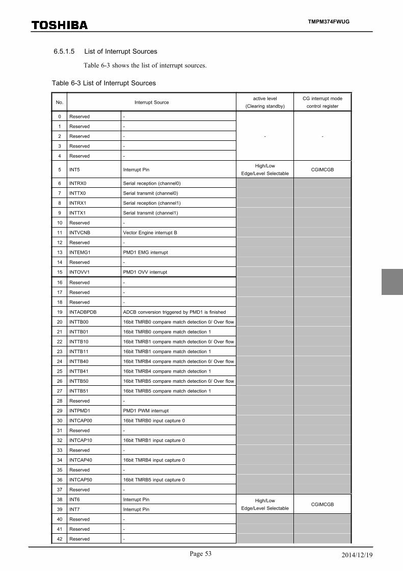
6.5.1.5 List of Interrupt Sources
Table 6-3 shows the list of interrupt sources.
Table 6-3 List of Interrupt Sources
No. Interrupt Sourceactive level
(Clearing standby)CG interrupt mode
control register
0 Reserved -
- -
1 Reserved -
2 Reserved -
3 Reserved -
4 Reserved -
5 INT5 Interrupt PinHigh/Low
Edge/Level SelectableCGIMCGB
6 INTRX0 Serial reception (channel0)
7 INTTX0 Serial transmit (channel0)
8 INTRX1 Serial reception (channel1)
9 INTTX1 Serial transmit (channel1)
10 Reserved -
11 INTVCNB Vector Engine interrupt B
12 Reserved -
13 INTEMG1 PMD1 EMG interrupt
14 Reserved -
15 INTOVV1 PMD1 OVV interrupt
16 Reserved -
17 Reserved -
18 Reserved -
19 INTADBPDB ADCB conversion triggered by PMD1 is finished
20 INTTB00 16bit TMRB0 compare match detection 0/ Over flow
21 INTTB01 16bit TMRB0 compare match detection 1
22 INTTB10 16bit TMRB1 compare match detection 0/ Over flow
23 INTTB11 16bit TMRB1 compare match detection 1
24 INTTB40 16bit TMRB4 compare match detection 0/ Over flow
25 INTTB41 16bit TMRB4 compare match detection 1
26 INTTB50 16bit TMRB5 compare match detection 0/ Over flow
27 INTTB51 16bit TMRB5 compare match detection 1
28 Reserved -
29 INTPMD1 PMD1 PWM interrupt
30 INTCAP00 16bit TMRB0 input capture 0
31 Reserved -
32 INTCAP10 16bit TMRB1 input capture 0
33 Reserved -
34 INTCAP40 16bit TMRB4 input capture 0
35 Reserved -
36 INTCAP50 16bit TMRB5 input capture 0
37 Reserved -
38 INT6 Interrupt Pin High/LowEdge/Level Selectable
CGIMCGB39 INT7 Interrupt Pin
40 Reserved -
41 Reserved -
42 Reserved -
TMPM374FWUG
Page 53 2014/12/19
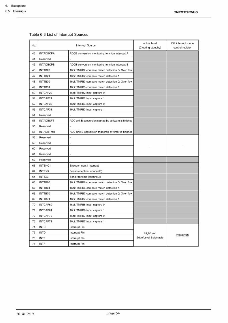
Table 6-3 List of Interrupt Sources
No. Interrupt Sourceactive level
(Clearing standby)CG interrupt mode
control register
43 INTADBCPA ADCB conversion monitoring function interrupt A
44 Reserved -
45 INTADBCPB ADCB conversion monitoring function interrupt B
46 INTTB20 16bit TMRB2 compare match detection 0/ Over flow
47 INTTB21 16bit TMRB2 compare match detection 1
48 INTTB30 16bit TMRB3 compare match detection 0/ Over flow
49 INTTB31 16bit TMRB3 compare match detection 1
50 INTCAP20 16bit TMRB2 input capture 0
51 INTCAP21 16bit TMRB2 input capture 1
52 INTCAP30 16bit TMRB3 input capture 0
53 INTCAP31 16bit TMRB3 input capture 1
54 Reserved -
55 INTADBSFT ADC unit B conversion started by software is finished
56 Reserved -
57 INTADBTMR ADC unit B conversion triggered by timer is finished
58 Reserved -
- -59 Reserved -
60 Reserved -
61 Reserved -
62 Reserved -
63 INTENC1 Encoder input1 interrupt
64 INTRX3 Serial reception (channel3)
65 INTTX3 Serial transmit (channel3)
66 INTTB60 16bit TMRB6 compare match detection 0/ Over flow
67 INTTB61 16bit TMRB6 compare match detection 1
68 INTTB70 16bit TMRB7 compare match detection 0/ Over flow
69 INTTB71 16bit TMRB7 compare match detection 1
70 INTCAP60 16bit TMRB6 input capture 0
71 INTCAP61 16bit TMRB6 input capture 1
72 INTCAP70 16bit TMRB7 input capture 0
73 INTCAP71 16bit TMRB7 input capture 1
74 INTC Interrupt Pin
High/LowEdge/Level Selectable
CGIMCGD75 INTD Interrupt Pin
76 INTE Interrupt Pin
77 INTF Interrupt Pin
TMPM374FWUG
6. Exceptions
6.5 Interrupts
Page 542014/12/19
6.5.1.6 Active level
The active level indicates which change in signal of an interrupt source triggers an interrupt. The CPU rec-ognizes interrupt signals in "High" level as interrupt. Interrupt signals directly sent from peripheral func-tions to the CPU are configured to output "High" to indicate an interrupt request.
Active level is set to the clock generator for interrupts which can be a trigger to release standby. Inter-rupt requests from peripheral functions are set as rising-edge or falling-edge triggered. Interrupt requestsfrom interrupt pins can be set as level-sensitive ("High" or "Low") or edge-triggered (rising or falling).
If an interrupt source is used for clearing a standby mode, setting the relevant clock generator registeris also required. Enable the CGIMCGx<INTxEN> bit and specify the active level in theCGIMCGx<EMCGx> bits. You must set the active level for interrupt requests from each peripheral func-tion as shown in Table 6-3
An interrupt request detected by the clock generator is notified to the CPU with a signal in "High" level.
TMPM374FWUG
Page 55 2014/12/19

6.5.2 Interrupt Handling
6.5.2.1 Flowchart
The following shows how an interrupt is handled.
The following shows how an exception/interrupt is handled. In the following descriptions, indicates hardware handling. indicates software handling.
TMPM374FWUG
6. Exceptions
6.5 Interrupts
Page 562014/12/19

Processing Details See
Setting for detection
Set the relevant NVIC registers for detecting interrupts.Set the clock generator as well if each interrupt source is used to clear a stand-by mode.ο Common settingNVIC registersο setting to clear standby modeClock generator
"6.5.2.2 Preparation"
setting for sending
interrupt signal
Execute an appropriate setting to send the interrupt signal depending on the in-terrupt type.ο Setting for interrupt from external pinPortο Setting for interrupt from peripheral functionPeripheral function (See the chapter of each peripheral function for details.)
Interrupt generation An interrupt request is generated.
CG detects interrupt(clearing standby mode)
Clearingstandby mode
Not clearingstandby mode
Interrupt lines used for clearing a standby mode are connected to the CPU viathe clock generator. "6.5.2.3 Detection by
Clock Generator"
CPU detects interrupt.
The CPU detects the interrupt.
"6.5.2.4 Detection byCPU"
If multiple interrupt requests occur simultaneously, the interrupt request withthe highest priority is detected according to the priority order.
CPU handles interrupt.
The CPU handles the interrupt. "6.5.2.5 CPU process-
ing"
The CPU pushes register contents to the stack before entering the ISR.
ISR execution Program for the ISR.Clear the interrupt source if needed.
"6.5.2.6 Interrupt Serv-ice Routine (ISR)"
Return to preceding
program Configure to return to the preceding program of the ISR.
TMPM374FWUG
Page 57 2014/12/19

6.5.2.2 Preparation
When preparing for an interrupt, you need to pay attention to the order of configuration to avoid any un-expected interrupt on the way.
Initiating an interrupt or changing its configuration must be implemented in the following order basical-ly. Disable the interrupt by the CPU. Configure from the farthest route from the CPU. Then enable the in-terrupt by the CPU.
To configure the clock generator, you must follow the order indicated here not to cause any unexpec-ted interrupt. First, configure the precondition. Secondly, clear the data related to the interrupt in theclock generator and then enable the interrupt.
The following sections are listed in the order of interrupt handling and describe how to configure them.
1. Disabling interrupt by CPU
2. CPU registers setting
3. Preconfiguration (1) (Interrupt from external pin)
4. Preconfiguration (2) (Interrupt from peripheral function)
5. Preconfiguration (3) (Interrupt Set-Pending Register)
6. Configuring the clock generator
7. Enabling interrupt by CPU
(1) Disabling interrupt by CPU
To make the CPU for not accepting any interrupt, write "1" to the corresponding bit of the PRI-MASK Register. All interrupts and exceptions other than non-maskable interrupts and hard faultscan be masked.
Use "MSR" instruction to set this register.
Interrupt mask register
PRIMASK ← "1"(Interrupt disabled)
Note 1: PRIMASK register cannot be modified by the user access level.Note 2: If a fault causes when "1" is set to the PRIMASK register, it is treated as a hard fault.
TMPM374FWUG
6. Exceptions
6.5 Interrupts
Page 582014/12/19

(2) CPU registers setting
You can assign a priority level by writing to <PRI_n> field in an Interrupt Priority Register ofthe NVIC register.
Each interrupt source is provided with eight bits for assigning a priority level from 0 to 255, butthe number of bits actually used varies with each product.Priority level 0 is the highest priority lev-el.If multiple sources have the same priority, the smallest-numbered interrupt source has the highestpriority.
You can assign grouping priority by using the <PRIGROUP> in the Application Interrupt and Re-set Control Register.
NVIC register
<PRI_n> ← "prioryty"
<PRIGROUP> ← "group priority" (This is configurable if required.)
Note:"n" indicates the corresponding exceptions/interrupts.This product uses three bits for assigning a priority level.
(3) Preconfiguration (1) (Interrupt from external pin)
Set "1" to the port function register of the corresponding pin. Setting PxFRn[m] allows the pin tobe used as the function pin. Setting PxIE[m] allows the pin to be used as the input port.
Port register
PxFRn<PxmFn> ← "1"
PxIE<PxmIE> ← "1"
Note:x: port number / m: corresponding bit / n: function register number In modes other thanSTOP mode, setting PxIE to enable input enables the corresponding interrupt input regard-less of the PxFR setting. Be careful not to enable interrupts that are not used. Also, beaware of the description of "6.5.1.4 Precautions when using external interrupt pins".
(4) Preconfiguration (2) (Interrupt from peripheral function)
The setting varies depending on the peripheral function to be used. See the chapter of each periph-eral function for details.
(5) Preconfiguration (3) (Interrupt Set-Pending Register)
To generate an interrupt by using the Interrupt Set-Pending Register, set "1" to the correspondingbit of this register.
NVIC register
Interrupt Set-Pending [m] ← "1"
Note:m: corresponding bit
TMPM374FWUG
Page 59 2014/12/19

(6) Configuring the clock generator
For an interrupt source to be used for exiting a standby mode, you need to set the active leveland enable interrupts in the CGIMCG register of the clock generator. The CGIMCG register is capa-ble of configuring each source.
Before enabling an interrupt, clear the corresponding interrupt request already held. This canavoid unexpected interrupt.To clear corresponding interrupt request, write a value corresponding tothe interrupt to be used to the CGICRCG register.See "6.6.3.3 CGICRCG (CG Interrupt RequestClear Register)" for each value.
Interrupt requests from external pins can be used without setting the clock generator if they arenot used for exiting a standby mode. However, an "High" pulse or "High"-level signal must be in-put so that the CPU can detect it as an interrupt request. Also, be aware of the description of"6.5.1.4 Precautions when using external interrupt pins".
Clock generator register
CGIMCGn<EMCGm> ← active level
CGICRCG<ICRCG> ← Value corresponding to the interrupt to be used
CGIMCGn<INTmEN> ← "1" (interrupt enabled)
Note:n: register number / m: number assigned to interrupt source
(7) Enabling interrupt by CPU
Enable the interrupt by the CPU as shown below.
Clear the suspended interrupt in the Interrupt Clear-Pending Register. Enable the intended inter-rupt with the Interrupt Set-Enable Register. Each bit of the register is assigned to a single interruptsource.
Writing "1" to the corresponding bit of the Interrupt Clear-Pending Register clears the suspended in-terrupt. Writing "1" to the corresponding bit of the Interrupt Set-Enable Register enables the inten-ded interrupt.
To generate interrupts in the Interrupt Set-Pending Register setting, factors to trigger interruptsare lost if pending interrupts are cleared. Thus, this operation is not necessary.
At the end, PRIMASK register is zero cleared.
NVIC register
Interrupt Clear-Pending [m] ← "1"
Interrupt Set-Pending [m] ← "1"
Interrupt mask register
PRIMASK ← "0"
Note 1: m : corresponding bitNote 2: PRIMASK register cannot be modified by the user access level.
TMPM374FWUG
6. Exceptions
6.5 Interrupts
Page 602014/12/19

6.5.2.3 Detection by Clock Generator
If an interrupt source is used for exiting a standby mode, an interrupt request is detected according tothe active level specified in the clock generator, and is notified to the CPU.
An edge-triggered interrupt request, once detected, is held in the clock generator. A level-sensitive inter-rupt request must be held at the active level until it is detected, otherwise the interrupt request will ceaseto exist when the signal level changes from active to inactive.
When the clock generator detects an interrupt request, it keeps sending the interrupt signal in "High" lev-el to the CPU until the interrupt request is cleared in the CG Interrupt Request Clear (CGICRCG) Regis-ter. If a standby mode is exited without clearing the interrupt request, the same interrupt will be detectedagain when normal operation is resumed. Be sure to clear each interrupt request in the ISR.
6.5.2.4 Detection by CPU
The CPU detects an interrupt request with the highest priority.
6.5.2.5 CPU processing
On detecting an interrupt, the CPU pushes the contents of PC, PSR, r0-r3, r12 and LR to the stack thenenter the ISR.
TMPM374FWUG
Page 61 2014/12/19
6.5.2.6 Interrupt Service Routine (ISR)
An ISR requires specific programming according to the application to be used. This section describeswhat is recommended at the service routine programming and how the source is cleared.
(1) Pushing during ISR
An ISR normally pushes register contents to the stack and handles an interrupt as required. The Cor-tex-M3 core automatically pushes the contents of PC, PSR, r0-r3, r12 and LR to the stack. No extraprogramming is required for them.
Push the contents of other registers if needed.
Interrupt requests with higher priority and exceptions such as NMI are accepted even when anISR is being executed. We recommend you to push the contents of general-purpose registers thatmight be rewritten.
(2) Clearing an interrupt source
If an interrupt source is used for clearing a standby mode, each interrupt request must be clearedwith the CG Interrupt Request Clear (CGICRCG) Register.
If an interrupt source is set as level-sensitive, an interrupt request continues to exist until it iscleared at its source. Therefore, the interrupt source must be cleared. Clearing the interrupt source au-tomatically clears the interrupt request signal from the clock generator.
If an interrupt is set as edge-sensitive, clear an interrupt request by setting the corresponding val-ue in the CGICRCG register. When an active edge occurs again, a new interrupt request will be detec-ted.
TMPM374FWUG
6. Exceptions
6.5 Interrupts
Page 622014/12/19

6.6 Exception / Interrupt-Related RegistersThe CPU's NVIC registers and clock generator registers described in this chapter are shown below with their re-
spective addresses.
6.6.1 Register List
NVIC registers Base Address = 0xE000_E000
Register name Address
SysTick Control and Status Register 0x0010
SysTick Reload Value Register 0x0014
SysTick Current Value Register 0x0018
SysTick Calibration Value Register 0x001C
Interrupt Set-Enable Register 1 0x0100
Interrupt Set-Enable Register 2 0x0104
Interrupt Set-Enable Register 3 0x0108
Interrupt Clear-Enable Register 1 0x0180
Interrupt Clear-Enable Register 2 0x0184
Interrupt Clear-Enable Register 3 0x0188
Interrupt Set-Pending Register 1 0x0200
Interrupt Set-Pending Register 2 0x0204
Interrupt Set-Pending Register 3 0x0208
Interrupt Clear-Pending Register 1 0x0280
Interrupt Clear-Pending Register 2 0x0284
Interrupt Clear-Pending Register 3 0x0288
Interrupt Priority Register 0x0400 to 0x0460
Vector Table Offset Register 0x0D08
Application Interrupt and Reset Control Register 0x0D0C
System Handler Priority Register 0x0D18, 0x0D1C, 0x0D20
System Handler Control and State Register 0x0D24
Clock generator register Base Address = 0x4004_0200
Register name Address
CG Interrupt Request Clear Register CGICRCG 0x0014
NMI Flag Register CGNMIFLG 0x0018
Reset Flag Register CGRSTFLG 0x001C
Reserved - 0x0020
CG Interrupt Mode Control Register B CGIMCGB 0x0024
Reserved - 0x0028
CG Interrupt Mode Control Register D CGIMCGD 0x002C
Reserved - 0x0030
Reserved - 0x0034
Reserved - 0x0038
Reserved - 0x003C
Note:Access to the "Reserved" areas is prohibited.
TMPM374FWUG
Page 63 2014/12/19

6.6.2 NVIC Registers
6.6.2.1 SysTick Control and Status Register
31 30 29 28 27 26 25 24
bit symbol - - - - - - - -
After reset 0 0 0 0 0 0 0 0
23 22 21 20 19 18 17 16
bit symbol - - - - - - - COUNTFLAG
After reset 0 0 0 0 0 0 0 0
15 14 13 12 11 10 9 8
bit symbol - - - - - - - -
After reset 0 0 0 0 0 0 0 0
7 6 5 4 3 2 1 0
bit symbol - - - - - CLKSOURCE TICKINT ENABLE
After reset 0 0 0 0 0 0 0 0
Bit Bit Symbol Type Function
31-17 − R Read as 0.
16 COUNTFLAG R/W 0: Timer not counted to 01: Timer counted to 0Returns "1" if timer counted to "0" since last time this was read.Clears on read of any part of the SysTick Control and Status Register.
15-3 − R Read as 0.
2 CLKSOURCE R/W 0: External reference clock (fosc/32) (Note)1: CPU clock (fsys)
1 TICKINT R/W 0: Do not pend SysTick1: Pend SysTick
0 ENABLE R/W 0: Disable1: EnableIf "1" is set, it reloads with the value of the Reload Value Register and starts operation.
Note:In this product, fosc which is selected by CGOSCCR <OSCSEL> by 32 is used as external refer-rence clock.
TMPM374FWUG
6. Exceptions
6.6 Exception / Interrupt-Related Registers
Page 642014/12/19
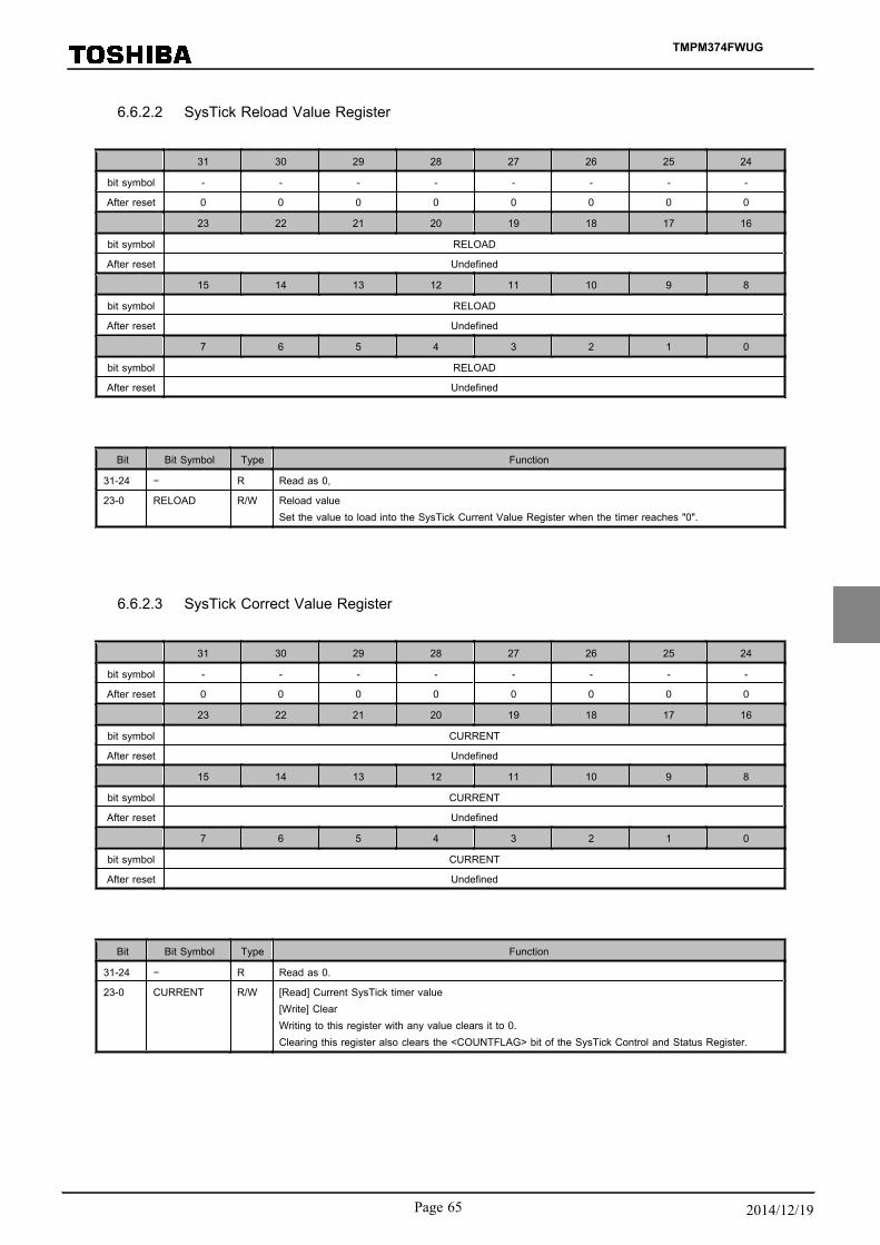
6.6.2.2 SysTick Reload Value Register
31 30 29 28 27 26 25 24
bit symbol - - - - - - - -
After reset 0 0 0 0 0 0 0 0
23 22 21 20 19 18 17 16
bit symbol RELOAD
After reset Undefined
15 14 13 12 11 10 9 8
bit symbol RELOAD
After reset Undefined
7 6 5 4 3 2 1 0
bit symbol RELOAD
After reset Undefined
Bit Bit Symbol Type Function
31-24 − R Read as 0,
23-0 RELOAD R/W Reload valueSet the value to load into the SysTick Current Value Register when the timer reaches "0".
6.6.2.3 SysTick Correct Value Register
31 30 29 28 27 26 25 24
bit symbol - - - - - - - -
After reset 0 0 0 0 0 0 0 0
23 22 21 20 19 18 17 16
bit symbol CURRENT
After reset Undefined
15 14 13 12 11 10 9 8
bit symbol CURRENT
After reset Undefined
7 6 5 4 3 2 1 0
bit symbol CURRENT
After reset Undefined
Bit Bit Symbol Type Function
31-24 − R Read as 0.
23-0 CURRENT R/W [Read] Current SysTick timer value[Write] ClearWriting to this register with any value clears it to 0.Clearing this register also clears the <COUNTFLAG> bit of the SysTick Control and Status Register.
TMPM374FWUG
Page 65 2014/12/19

6.6.2.4 SysTick Calibration Value Register
31 30 29 28 27 26 25 24
bit symbol NOREF SKEW - - - - - -
After reset 0 0 0 0 0 0 0 0
23 22 21 20 19 18 17 16
bit symbol TENMS
After reset 0 0 0 0 0 0 0 0
15 14 13 12 11 10 9 8
bit symbol TENMS
After reset 0 0 0 0 1 0 0 1
7 6 5 4 3 2 1 0
bit symbol TENMS
After reset 1 1 0 0 0 1 0 0
Bit Bit Symbol Type Function
31 NOREF R 0: Reference clock provided1: No reference clock
30 SKEW R 0: Calibration value is 10 ms.1: Calibration value is not 10ms.
29-24 − R Read as 0.
23-0 TENMS R Calibration valueReload value to use for 10 ms timing (0xC35) by external reffernce clock. (Note)
Note:In the case of a multishot, please use <TENMS>-1.
TMPM374FWUG
6. Exceptions
6.6 Exception / Interrupt-Related Registers
Page 662014/12/19

6.6.2.5 Interrupt Set-Enable Register 1
31 30 29 28 27 26 25 24
bit symbol -SETENA
(Interrupt 30)SETENA
(Interrupt 29)-
SETENA(Interrupt 27)
SETENA(Interrupt 26)
SETENA(Interrupt 25)
SETENA(Interrupt 24)
After reset 0 0 0 0 0 0 0 0
23 22 21 20 19 18 17 16
bit symbolSETENA
(Interrupt 23)SETENA
(Interrupt 22)SETENA
(Interrupt 21)SETENA
(Interrupt 20)SETENA
(Interrupt 19)- - -
After reset 0 0 0 0 0 0 0 0
15 14 13 12 11 10 9 8
bit symbolSETENA
(Interrupt 15)-
SETENA(Interrupt 13)
-SETENA
(Interrupt 11)-
SETENA(Interrupt 9)
SETENA(Interrupt 8)
After reset 0 0 0 0 0 0 0 0
7 6 5 4 3 2 1 0
bit symbolSETENA
(Interrupt 7)SETENA
(Interrupt 6)SETENA
(Interrupt 5)- - - - -
After reset 0 0 0 0 0 0 0 0
Bit Bit Symbol Type Function
31 − R/W Write as 0.
30-29 SETENA R/W Interrupt number [30:29][Write]1: Enable[Read]0: Disabled1: EnabledEach bit corresponds to the specified number of interrupts.Writing "1" to a bit in this register enables the corresponding interrupt. Writing "0" has no effect.Reading the bits can see the enable/disable condition of the corresponding interrupts.
28 − R/W Write as 0.
27-19 SETENA R/W Interrupt number [27:19][Write]1: Enable[Read]0: Disabled1: EnabledEach bit corresponds to the specified number of interrupts.Writing "1" to a bit in this register enables the corresponding interrupt. Writing "0" has no effect.Reading the bits can see the enable/disable condition of the corresponding interrupts.
18-16 − R/W Write as 0.
15 SETENA R/W Interrupt number [15][Write]1: Enable[Read]0: Disabled1: EnabledEach bit corresponds to the specified number of interrupts.Writing "1" to a bit in this register enables the corresponding interrupt. Writing "0" has no effect.Reading the bits can see the enable/disable condition of the corresponding interrupts.
14 − R/W Write as 0.
TMPM374FWUG
Page 67 2014/12/19

Bit Bit Symbol Type Function
13 SETENA R/W Interrupt number [13][Write]1: Enable[Read]0: Disabled1: EnabledEach bit corresponds to the specified number of interrupts.Writing "1" to a bit in this register enables the corresponding interrupt. Writing "0" has no effect.Reading the bits can see the enable/disable condition of the corresponding interrupts.
12 − R/W Write as 0.
11 SETENA R/W Interrupt number [11][Write]1: Enable[Read]0: Disabled1: EnabledEach bit corresponds to the specified number of interrupts.Writing "1" to a bit in this register enables the corresponding interrupt. Writing "0" has no effect.Reading the bits can see the enable/disable condition of the corresponding interrupts.
10 − R/W Write as 0.
9-5 SETENA R/W Interrupt number [9:5][Write]1: Enable[Read]0: Disabled1: EnabledEach bit corresponds to the specified number of interrupts.Writing "1" to a bit in this register enables the corresponding interrupt. Writing "0" has no effect.Reading the bits can see the enable/disable condition of the corresponding interrupts.
4-0 − R/W Write as 0.
Note:For descriptions of interrupts and interrupt numbers, see Section "6.5.1.5 List of Interrupt Sources".
TMPM374FWUG
6. Exceptions
6.6 Exception / Interrupt-Related Registers
Page 682014/12/19

6.6.2.6 Interrupt Set-Enable Register 2
31 30 29 28 27 26 25 24
bit symbolSETENA
(Interrupt 63)- - - - -
SETENA(Interrupt 57)
-
After reset 0 0 0 0 0 0 0 0
23 22 21 20 19 18 17 16
bit symbolSETENA
(Interrupt 55)-
SETENA(Interrupt 53)
SETENA(Interrupt 52)
SETENA(Interrupt 51)
SETENA(Interrupt 50)
SETENA(Interrupt 49)
SETENA(Interrupt 48)
After reset 0 0 0 0 0 0 0 0
15 14 13 12 11 10 9 8
bit symbolSETENA
(Interrupt 47)SETENA
(Interrupt 46)SETENA
(Interrupt 45)-
SETENA(Interrupt 43)
- - -
After reset 0 0 0 0 0 0 0 0
7 6 5 4 3 2 1 0
bit symbolSETENA
(Interrupt 39)SETENA
(Interrupt 38)-
SETENA(Interrupt 36)
-SETENA
(Interrupt 34)-
SETENA(Interrupt 32)
After reset 0 0 0 0 0 0 0 0
Bit Bit Symbol Type Function
31 SETENA R/W Interrupt number [63][Write]1: Enable[Read]0: Disabled1: EnabledEach bit corresponds to the specified number of interrupts.Writing "1" to a bit in this register enables the corresponding interrupt. Writing "0" has no effect.Reading the bits can see the enable/disable condition of the corresponding interrupts.
30-26 − R/W Write as 0.
25 SETENA R/W Interrupt number [57][Write]1: Enable[Read]0: Disabled1: EnabledEach bit corresponds to the specified number of interrupts.Writing "1" to a bit in this register enables the corresponding interrupt. Writing "0" has no effect.Reading the bits can see the enable/disable condition of the corresponding interrupts.
24 − R/W Write as 0.
23 SETENA R/W Interrupt number [55][Write]1: Enable[Read]0: Disabled1: EnabledEach bit corresponds to the specified number of interrupts.Writing "1" to a bit in this register enables the corresponding interrupt. Writing "0" has no effect.Reading the bits can see the enable/disable condition of the corresponding interrupts.
22 − R/W Write as 0.
TMPM374FWUG
Page 69 2014/12/19

Bit Bit Symbol Type Function
21-13 SETENA R/W Interrupt number [53:45][Write]1: Enable[Read]0: Disabled1: EnabledEach bit corresponds to the specified number of interrupts.Writing "1" to a bit in this register enables the corresponding interrupt. Writing "0" has no effect.Reading the bits can see the enable/disable condition of the corresponding interrupts.
12 − R/W Write as 0.
11 SETENA R/W Interrupt number [43][Write]1: Enable[Read]0: Disabled1: EnabledEach bit corresponds to the specified number of interrupts.Writing "1" to a bit in this register enables the corresponding interrupt. Writing "0" has no effect.Reading the bits can see the enable/disable condition of the corresponding interrupts.
10-8 − R/W Write as 0.
7-6 SETENA R/W Interrupt number [39:38][Write]1: Enable[Read]0: Disabled1: EnabledEach bit corresponds to the specified number of interrupts.Writing "1" to a bit in this register enables the corresponding interrupt. Writing "0" has no effect.Reading the bits can see the enable/disable condition of the corresponding interrupts.
5 − R/W Write as 0.
4 SETENA R/W Interrupt number [36][Write]1: Enable[Read]0: Disabled1: EnabledEach bit corresponds to the specified number of interrupts.Writing "1" to a bit in this register enables the corresponding interrupt. Writing "0" has no effect.Reading the bits can see the enable/disable condition of the corresponding interrupts.
3 − R/W Write as 0.
2 SETENA R/W Interrupt number [34][Write]1: Enable[Read]0: Disabled1: EnabledEach bit corresponds to the specified number of interrupts.Writing "1" to a bit in this register enables the corresponding interrupt. Writing "0" has no effect.Reading the bits can see the enable/disable condition of the corresponding interrupts.
1 − R/W Write as 0.
TMPM374FWUG
6. Exceptions
6.6 Exception / Interrupt-Related Registers
Page 702014/12/19
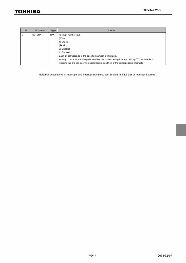
Bit Bit Symbol Type Function
0 SETENA R/W Interrupt number [32][Write]1: Enable[Read]0: Disabled1: EnabledEach bit corresponds to the specified number of interrupts.Writing "1" to a bit in this register enables the corresponding interrupt. Writing "0" has no effect.Reading the bits can see the enable/disable condition of the corresponding interrupts.
Note:For descriptions of interrupts and interrupt numbers, see Section "6.5.1.5 List of Interrupt Sources".
TMPM374FWUG
Page 71 2014/12/19

6.6.2.7 Interrupt Set-Enable Register 3
31 30 29 28 27 26 25 24
bit symbol - - - - - - - -
After reset 0 0 0 0 0 0 0 0
23 22 21 20 19 18 17 16
bit symbol - - - - - - - -
After reset 0 0 0 0 0 0 0 0
15 14 13 12 11 10 9 8
bit symbol - -SETENA
(Interrupt 77)SETENA
(Interrupt 76)SETENA
(Interrupt 75)SETENA
(Interrupt 74)SETENA
(Interrupt 73)SETENA
(Interrupt 72)
After reset 0 0 0 0 0 0 0 0
7 6 5 4 3 2 1 0
bit symbolSETENA
(Interrupt 71)SETENA
(Interrupt 70)SETENA
(Interrupt 69)SETENA
(Interrupt 68)SETENA
(Interrupt 67)SETENA
(Interrupt 66)SETENA
(Interrupt 65)SETENA
(Interrupt 64)
After reset 0 0 0 0 0 0 0 0
Bit Bit Symbol Type Function
31-14 − R/W Read as 0.
13-0 SETENA R/W Interrupt number [77:64][Write]1: Enable[Read]0: Disabled1: EnabledEach bit corresponds to the specified number of interrupts.Writing "1" to a bit in this register enables the corresponding interrupt. Writing "0" has no effect.Reading the bits can see the enable/disable condition of the corresponding interrupts.
Note:For descriptions of interrupts and interrupt numbers, see Section "6.5.1.5 List of Interrupt Sources".
TMPM374FWUG
6. Exceptions
6.6 Exception / Interrupt-Related Registers
Page 722014/12/19
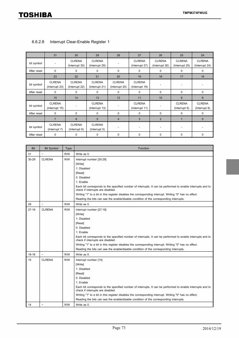
6.6.2.8 Interrupt Clear-Enable Register 1
31 30 29 28 27 26 25 24
bit symbol -CLRENA
(Interrupt 30)CLRENA
(Interrupt 29)-
CLRENA(Interrupt 27)
CLRENA(Interrupt 26)
CLRENA(Interrupt 25)
CLRENA(Interrupt 24)
After reset 0 0 0 0 0 0 0 0
23 22 21 20 19 18 17 16
bit symbolCLRENA
(Interrupt 23)CLRENA
(Interrupt 22)CLRENA
(Interrupt 21)CLRENA
(Interrupt 20)CLRENA
(Interrupt 19)- - -
After reset 0 0 0 0 0 0 0 0
15 14 13 12 11 10 9 8
bit symbolCLRENA
(Interrupt 15)-
CLRENA(Interrupt 13)
-CLRENA
(Interrupt 11)-
CLRENA(Interrupt 9)
CLRENA(Interrupt 8)
After reset 0 0 0 0 0 0 0 0
7 6 5 4 3 2 1 0
bit symbolCLRENA
(Interrupt 7)CLRENA
(Interrupt 6)CLRENA
(Interrupt 5)- - - - -
After reset 0 0 0 0 0 0 0 0
Bit Bit Symbol Type Function
31 − R/W Write as 0.
30-29 CLRENA R/W Interrupt number [30:29][Write]1: Disabled[Read]0: Disabled1: EnableEach bit corresponds to the specified number of interrupts. It can be performed to enable interrupts and tocheck if interrupts are disabled.Writing "1" to a bit in this register disables the corresponding interrupt. Writing "0" has no effect.Reading the bits can see the enable/disable condition of the corresponding interrupts.
28 − R/W Write as 0.
27-19 CLRENA R/W Interrupt number [27:19][Write]1: Disabled[Read]0: Disabled1: EnableEach bit corresponds to the specified number of interrupts. It can be performed to enable interrupts and tocheck if interrupts are disabled.Writing "1" to a bit in this register disables the corresponding interrupt. Writing "0" has no effect.Reading the bits can see the enable/disable condition of the corresponding interrupts.
18-16 − R/W Write as 0.
15 CLRENA R/W Interrupt number [15][Write]1: Disabled[Read]0: Disabled1: EnableEach bit corresponds to the specified number of interrupts. It can be performed to enable interrupts and tocheck if interrupts are disabled.Writing "1" to a bit in this register disables the corresponding interrupt. Writing "0" has no effect.Reading the bits can see the enable/disable condition of the corresponding interrupts.
14 − R/W Write as 0.
TMPM374FWUG
Page 73 2014/12/19

Bit Bit Symbol Type Function
13 CLRENA R/W Interrupt number [13][Write]1: Disabled[Read]0: Disabled1: EnableEach bit corresponds to the specified number of interrupts. It can be performed to enable interrupts and tocheck if interrupts are disabled.Writing "1" to a bit in this register disables the corresponding interrupt. Writing "0" has no effect.Reading the bits can see the enable/disable condition of the corresponding interrupts.
12 − R/W Write as 0.
11 CLRENA R/W Interrupt number [11][Write]1: Disabled[Read]0: Disabled1: EnableEach bit corresponds to the specified number of interrupts. It can be performed to enable interrupts and tocheck if interrupts are disabled.Writing "1" to a bit in this register disables the corresponding interrupt. Writing "0" has no effect.Reading the bits can see the enable/disable condition of the corresponding interrupts.
10 − R/W Write as 0.
9-5 CLRENA R/W Interrupt number [9:5][Write]1: Disabled[Read]0: Disabled1: EnableEach bit corresponds to the specified number of interrupts. It can be performed to enable interrupts and tocheck if interrupts are disabled.Writing "1" to a bit in this register disables the corresponding interrupt. Writing "0" has no effect.Reading the bits can see the enable/disable condition of the corresponding interrupts.
4-0 − R/W Write as 0.
Note:For descriptions of interrupts and interrupt numbers, see Section "6.5.1.5 List of Interrupt Sources".
TMPM374FWUG
6. Exceptions
6.6 Exception / Interrupt-Related Registers
Page 742014/12/19

6.6.2.9 Interrupt Clear-Enable Register 2
31 30 29 28 27 26 25 24
bit symbolCLRENA
(Interrupt 63)- - - - -
CLRENA(Interrupt 57)
-
After reset 0 0 0 0 0 0 0 0
23 22 21 20 19 18 17 16
bit symbolCLRENA
(Interrupt 55)-
CLRENA(Interrupt 53)
CLRENA(Interrupt 52)
CLRENA(Interrupt 51)
CLRENA(Interrupt 50)
CLRENA(Interrupt 49)
CLRENA(Interrupt 48)
After reset 0 0 0 0 0 0 0 0
15 14 13 12 11 10 9 8
bit symbolCLRENA
(Interrupt 47)CLRENA
(Interrupt 46)CLRENA
(Interrupt 45)-
CLRENA(Interrupt 43)
- - -
After reset 0 0 0 0 0 0 0 0
7 6 5 4 3 2 1 0
bit symbolCLRENA
(Interrupt 39)CLRENA
(Interrupt 38)-
CLRENA(Interrupt 36)
-CLRENA
(Interrupt 34)-
CLRENA(Interrupt 32)
After reset 0 0 0 0 0 0 0 0
Bit Bit Symbol Type Function
31 CLRENA R/W Interrupt number [63][Write]1: Disabled[Read]0: Disabled1: EnableEach bit corresponds to the specified number of interrupts. It can be performed to enable interrupts and tocheck if interrupts are disabled.Writing "1" to a bit in this register disables the corresponding interrupt. Writing "0" has no effect.Reading the bits can see the enable/disable condition of the corresponding interrupts.
30-26 − R/W Write as 0.
25 CLRENA R/W Interrupt number [57][Write]1: Disabled[Read]0: Disabled1: EnableEach bit corresponds to the specified number of interrupts. It can be performed to enable interrupts and tocheck if interrupts are disabled.Writing "1" to a bit in this register disables the corresponding interrupt. Writing "0" has no effect.Reading the bits can see the enable/disable condition of the corresponding interrupts.
24 − R/W Write as 0.
23 CLRENA R/W Interrupt number [55][Write]1: Disabled[Read]0: Disabled1: EnableEach bit corresponds to the specified number of interrupts. It can be performed to enable interrupts and tocheck if interrupts are disabled.Writing "1" to a bit in this register disables the corresponding interrupt. Writing "0" has no effect.Reading the bits can see the enable/disable condition of the corresponding interrupts.
22 − R/W Write as 0.
TMPM374FWUG
Page 75 2014/12/19
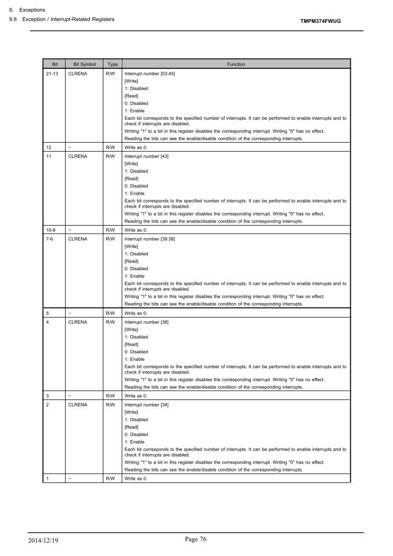
Bit Bit Symbol Type Function
21-13 CLRENA R/W Interrupt number [53:45][Write]1: Disabled[Read]0: Disabled1: EnableEach bit corresponds to the specified number of interrupts. It can be performed to enable interrupts and tocheck if interrupts are disabled.Writing "1" to a bit in this register disables the corresponding interrupt. Writing "0" has no effect.Reading the bits can see the enable/disable condition of the corresponding interrupts.
12 − R/W Write as 0.
11 CLRENA R/W Interrupt number [43][Write]1: Disabled[Read]0: Disabled1: EnableEach bit corresponds to the specified number of interrupts. It can be performed to enable interrupts and tocheck if interrupts are disabled.Writing "1" to a bit in this register disables the corresponding interrupt. Writing "0" has no effect.Reading the bits can see the enable/disable condition of the corresponding interrupts.
10-8 − R/W Write as 0.
7-6 CLRENA R/W Interrupt number [39:38][Write]1: Disabled[Read]0: Disabled1: EnableEach bit corresponds to the specified number of interrupts. It can be performed to enable interrupts and tocheck if interrupts are disabled.Writing "1" to a bit in this register disables the corresponding interrupt. Writing "0" has no effect.Reading the bits can see the enable/disable condition of the corresponding interrupts.
5 − R/W Write as 0.
4 CLRENA R/W Interrupt number [36][Write]1: Disabled[Read]0: Disabled1: EnableEach bit corresponds to the specified number of interrupts. It can be performed to enable interrupts and tocheck if interrupts are disabled.Writing "1" to a bit in this register disables the corresponding interrupt. Writing "0" has no effect.Reading the bits can see the enable/disable condition of the corresponding interrupts.
3 − R/W Write as 0.
2 CLRENA R/W Interrupt number [34][Write]1: Disabled[Read]0: Disabled1: EnableEach bit corresponds to the specified number of interrupts. It can be performed to enable interrupts and tocheck if interrupts are disabled.Writing "1" to a bit in this register disables the corresponding interrupt. Writing "0" has no effect.Reading the bits can see the enable/disable condition of the corresponding interrupts.
1 − R/W Write as 0.
TMPM374FWUG
6. Exceptions
6.6 Exception / Interrupt-Related Registers
Page 762014/12/19
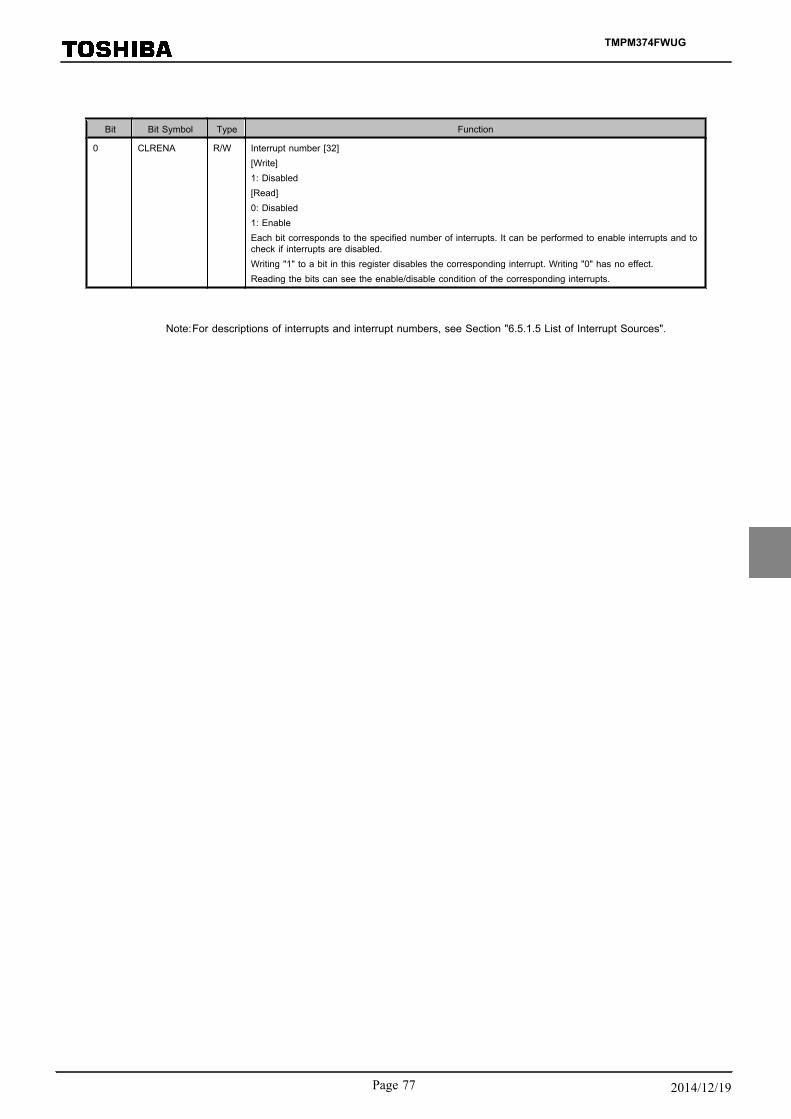
Bit Bit Symbol Type Function
0 CLRENA R/W Interrupt number [32][Write]1: Disabled[Read]0: Disabled1: EnableEach bit corresponds to the specified number of interrupts. It can be performed to enable interrupts and tocheck if interrupts are disabled.Writing "1" to a bit in this register disables the corresponding interrupt. Writing "0" has no effect.Reading the bits can see the enable/disable condition of the corresponding interrupts.
Note:For descriptions of interrupts and interrupt numbers, see Section "6.5.1.5 List of Interrupt Sources".
TMPM374FWUG
Page 77 2014/12/19
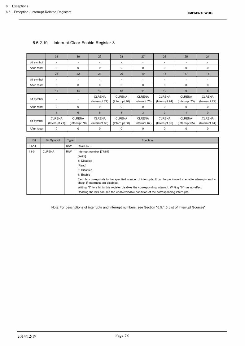
6.6.2.10 Interrupt Clear-Enable Register 3
31 30 29 28 27 26 25 24
bit symbol - - - - - - - -
After reset 0 0 0 0 0 0 0 0
23 22 21 20 19 18 17 16
bit symbol - - - - - - - -
After reset 0 0 0 0 0 0 0 0
15 14 13 12 11 10 9 8
bit symbol - -CLRENA
(Interrupt 77)CLRENA
(Interrupt 76)CLRENA
(Interrupt 75)CLRENA
(Interrupt 74)CLRENA
(Interrupt 73)CLRENA
(Interrupt 72)
After reset 0 0 0 0 0 0 0 0
7 6 5 4 3 2 1 0
bit symbolCLRENA
(Interrupt 71)CLRENA
(Interrupt 70)CLRENA
(Interrupt 69)CLRENA
(Interrupt 68)CLRENA
(Interrupt 67)CLRENA
(Interrupt 66)CLRENA
(Interrupt 65)CLRENA
(Interrupt 64)
After reset 0 0 0 0 0 0 0 0
Bit Bit Symbol Type Function
31-14 − R/W Read as 0.
13-0 CLRENA R/W Interrupt number [77:64][Write]1: Disabled[Read]0: Disabled1: EnableEach bit corresponds to the specified number of interrupts. It can be performed to enable interrupts and tocheck if interrupts are disabled.Writing "1" to a bit in this register disables the corresponding interrupt. Writing "0" has no effect.Reading the bits can see the enable/disable condition of the corresponding interrupts.
Note:For descriptions of interrupts and interrupt numbers, see Section "6.5.1.5 List of Interrupt Sources".
TMPM374FWUG
6. Exceptions
6.6 Exception / Interrupt-Related Registers
Page 782014/12/19

6.6.2.11 Interrupt Set-Pending Register 1
31 30 29 28 27 26 25 24
bit symbol -SETPEND
(Interrupt 30)SETPEND
(Interrupt 29)-
SETPEND(Interrupt 27)
SETPEND(Interrupt 26)
SETPEND(Interrupt 25)
SETPEND(Interrupt 24)
After reset Undefined Undefined Undefined Undefined Undefined Undefined Undefined Undefined
23 22 21 20 19 18 17 16
bit symbolSETPEND
(Interrupt 23)SETPEND
(Interrupt 22)SETPEND
(Interrupt 21)SETPEND
(Interrupt 20)SETPEND
(Interrupt 19)- - -
After reset Undefined Undefined Undefined Undefined Undefined Undefined Undefined Undefined
15 14 13 12 11 10 9 8
bit symbolSETPEND
(Interrupt 15)-
SETPEND(Interrupt 13)
-SETPEND
(Interrupt 11)-
SETPEND(Interrupt 9)
SETPEND(Interrupt 8)
After reset Undefined Undefined Undefined Undefined Undefined Undefined Undefined Undefined
7 6 5 4 3 2 1 0
bit symbolSETPEND
(Interrupt 7)SETPEND
(Interrupt 6)SETPEND
(Interrupt 5)- - - - -
After reset Undefined Undefined Undefined Undefined Undefined Undefined Undefined Undefined
Bit Bit Symbol Type Function
31 − R/W Write as 0.
30-29 SETPEND R/W Interrupt number [30:29][Write]1: Pend[Read]0: Not pending1: PendingEach bit corresponds to the specified number can force interrupts into the pending state and determineswhich interrupts are currently pending.Writing "1" to a bit in this register pends the corresponding interrupt. However, writing "1" has no effect onan interrupt that is already pending or is disabled. Writing "0" has no effect.Reading the bit returns the current state of the corresponding interrupts.Writing "1" to a corresponding bit in the Interrupt Clear-Pending Register clears the bit in this register.
28 − R/W Write as 0.
27-19 SETPEND R/W Interrupt number [27:19][Write]1: Pend[Read]0: Not pending1: PendingEach bit corresponds to the specified number can force interrupts into the pending state and determineswhich interrupts are currently pending.Writing "1" to a bit in this register pends the corresponding interrupt. However, writing "1" has no effect onan interrupt that is already pending or is disabled. Writing "0" has no effect.Reading the bit returns the current state of the corresponding interrupts.Writing "1" to a corresponding bit in the Interrupt Clear-Pending Register clears the bit in this register.
18-16 − R/W Write as 0.
TMPM374FWUG
Page 79 2014/12/19
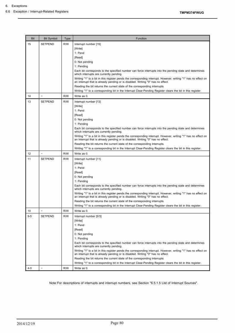
Bit Bit Symbol Type Function
15 SETPEND R/W Interrupt number [15][Write]1: Pend[Read]0: Not pending1: PendingEach bit corresponds to the specified number can force interrupts into the pending state and determineswhich interrupts are currently pending.Writing "1" to a bit in this register pends the corresponding interrupt. However, writing "1" has no effect onan interrupt that is already pending or is disabled. Writing "0" has no effect.Reading the bit returns the current state of the corresponding interrupts.Writing "1" to a corresponding bit in the Interrupt Clear-Pending Register clears the bit in this register.
14 − R/W Write as 0.
13 SETPEND R/W Interrupt number [13][Write]1: Pend[Read]0: Not pending1: PendingEach bit corresponds to the specified number can force interrupts into the pending state and determineswhich interrupts are currently pending.Writing "1" to a bit in this register pends the corresponding interrupt. However, writing "1" has no effect onan interrupt that is already pending or is disabled. Writing "0" has no effect.Reading the bit returns the current state of the corresponding interrupts.Writing "1" to a corresponding bit in the Interrupt Clear-Pending Register clears the bit in this register.
12 − R/W Write as 0.
11 SETPEND R/W Interrupt number [11][Write]1: Pend[Read]0: Not pending1: PendingEach bit corresponds to the specified number can force interrupts into the pending state and determineswhich interrupts are currently pending.Writing "1" to a bit in this register pends the corresponding interrupt. However, writing "1" has no effect onan interrupt that is already pending or is disabled. Writing "0" has no effect.Reading the bit returns the current state of the corresponding interrupts.Writing "1" to a corresponding bit in the Interrupt Clear-Pending Register clears the bit in this register.
10 − R/W Write as 0.
9-5 SETPEND R/W Interrupt number [9:5][Write]1: Pend[Read]0: Not pending1: PendingEach bit corresponds to the specified number can force interrupts into the pending state and determineswhich interrupts are currently pending.Writing "1" to a bit in this register pends the corresponding interrupt. However, writing "1" has no effect onan interrupt that is already pending or is disabled. Writing "0" has no effect.Reading the bit returns the current state of the corresponding interrupts.Writing "1" to a corresponding bit in the Interrupt Clear-Pending Register clears the bit in this register.
4-0 − R/W Write as 0.
Note:For descriptions of interrupts and interrupt numbers, see Section "6.5.1.5 List of Interrupt Sources".
TMPM374FWUG
6. Exceptions
6.6 Exception / Interrupt-Related Registers
Page 802014/12/19
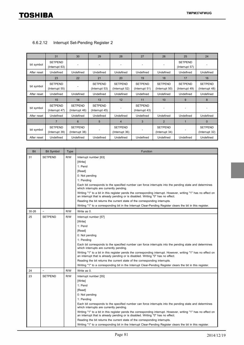
6.6.2.12 Interrupt Set-Pending Register 2
31 30 29 28 27 26 25 24
bit symbolSETPEND
(Interrupt 63)- - - - -
SETPEND(Interrupt 57)
-
After reset Undefined Undefined Undefined Undefined Undefined Undefined Undefined Undefined
23 22 21 20 19 18 17 16
bit symbolSETPEND
(Interrupt 55)-
SETPEND(Interrupt 53)
SETPEND(Interrupt 52)
SETPEND(Interrupt 51)
SETPEND(Interrupt 50)
SETPEND(Interrupt 49)
SETPEND(Interrupt 48)
After reset Undefined Undefined Undefined Undefined Undefined Undefined Undefined Undefined
15 14 13 12 11 10 9 8
bit symbolSETPEND
(Interrupt 47)SETPEND
(Interrupt 46)SETPEND
(Interrupt 45)-
SETPEND(Interrupt 43)
- - -
After reset Undefined Undefined Undefined Undefined Undefined Undefined Undefined Undefined
7 6 5 4 3 2 1 0
bit symbolSETPEND
(Interrupt 39)SETPEND
(Interrupt 38)-
SETPEND(Interrupt 36)
-SETPEND
(Interrupt 34)-
SETPEND(Interrupt 32)
After reset Undefined Undefined Undefined Undefined Undefined Undefined Undefined Undefined
Bit Bit Symbol Type Function
31 SETPEND R/W Interrupt number [63][Write]1: Pend[Read]0: Not pending1: PendingEach bit corresponds to the specified number can force interrupts into the pending state and determineswhich interrupts are currently pending.Writing "1" to a bit in this register pends the corresponding interrupt. However, writing "1" has no effect onan interrupt that is already pending or is disabled. Writing "0" has no effect.Reading the bit returns the current state of the corresponding interrupts.Writing "1" to a corresponding bit in the Interrupt Clear-Pending Register clears the bit in this register.
30-26 − R/W Write as 0.
25 SETPEND R/W Interrupt number [57][Write]1: Pend[Read]0: Not pending1: PendingEach bit corresponds to the specified number can force interrupts into the pending state and determineswhich interrupts are currently pending.Writing "1" to a bit in this register pends the corresponding interrupt. However, writing "1" has no effect onan interrupt that is already pending or is disabled. Writing "0" has no effect.Reading the bit returns the current state of the corresponding interrupts.Writing "1" to a corresponding bit in the Interrupt Clear-Pending Register clears the bit in this register.
24 − R/W Write as 0.
23 SETPEND R/W Interrupt number [55][Write]1: Pend[Read]0: Not pending1: PendingEach bit corresponds to the specified number can force interrupts into the pending state and determineswhich interrupts are currently pending.Writing "1" to a bit in this register pends the corresponding interrupt. However, writing "1" has no effect onan interrupt that is already pending or is disabled. Writing "0" has no effect.Reading the bit returns the current state of the corresponding interrupts.Writing "1" to a corresponding bit in the Interrupt Clear-Pending Register clears the bit in this register.
TMPM374FWUG
Page 81 2014/12/19

Bit Bit Symbol Type Function
22 − R/W Write as 0.
21-13 SETPEND R/W Interrupt number [53:45][Write]1: Pend[Read]0: Not pending1: PendingEach bit corresponds to the specified number can force interrupts into the pending state and determineswhich interrupts are currently pending.Writing "1" to a bit in this register pends the corresponding interrupt. However, writing "1" has no effect onan interrupt that is already pending or is disabled. Writing "0" has no effect.Reading the bit returns the current state of the corresponding interrupts.Writing "1" to a corresponding bit in the Interrupt Clear-Pending Register clears the bit in this register.
12 − R/W Write as 0.
11 SETPEND R/W Interrupt number [43][Write]1: Pend[Read]0: Not pending1: PendingEach bit corresponds to the specified number can force interrupts into the pending state and determineswhich interrupts are currently pending.Writing "1" to a bit in this register pends the corresponding interrupt. However, writing "1" has no effect onan interrupt that is already pending or is disabled. Writing "0" has no effect.Reading the bit returns the current state of the corresponding interrupts.Writing "1" to a corresponding bit in the Interrupt Clear-Pending Register clears the bit in this register.
10-8 − R/W Write as 0.
7-6 SETPEND R/W Interrupt number [39:38][Write]1: Pend[Read]0: Not pending1: PendingEach bit corresponds to the specified number can force interrupts into the pending state and determineswhich interrupts are currently pending.Writing "1" to a bit in this register pends the corresponding interrupt. However, writing "1" has no effect onan interrupt that is already pending or is disabled. Writing "0" has no effect.Reading the bit returns the current state of the corresponding interrupts.Writing "1" to a corresponding bit in the Interrupt Clear-Pending Register clears the bit in this register.
5 − R/W Write as 0.
4 SETPEND R/W Interrupt number [36][Write]1: Pend[Read]0: Not pending1: PendingEach bit corresponds to the specified number can force interrupts into the pending state and determineswhich interrupts are currently pending.Writing "1" to a bit in this register pends the corresponding interrupt. However, writing "1" has no effect onan interrupt that is already pending or is disabled. Writing "0" has no effect.Reading the bit returns the current state of the corresponding interrupts.Writing "1" to a corresponding bit in the Interrupt Clear-Pending Register clears the bit in this register.
3 − R/W Write as 0.
TMPM374FWUG
6. Exceptions
6.6 Exception / Interrupt-Related Registers
Page 822014/12/19

Bit Bit Symbol Type Function
2 SETPEND R/W Interrupt number [34][Write]1: Pend[Read]0: Not pending1: PendingEach bit corresponds to the specified number can force interrupts into the pending state and determineswhich interrupts are currently pending.Writing "1" to a bit in this register pends the corresponding interrupt. However, writing "1" has no effect onan interrupt that is already pending or is disabled. Writing "0" has no effect.Reading the bit returns the current state of the corresponding interrupts.Writing "1" to a corresponding bit in the Interrupt Clear-Pending Register clears the bit in this register.
1 − R/W Write as 0.
0 SETPEND R/W Interrupt number [32][Write]1: Pend[Read]0: Not pending1: PendingEach bit corresponds to the specified number can force interrupts into the pending state and determineswhich interrupts are currently pending.Writing "1" to a bit in this register pends the corresponding interrupt. However, writing "1" has no effect onan interrupt that is already pending or is disabled. Writing "0" has no effect.Reading the bit returns the current state of the corresponding interrupts.Writing "1" to a corresponding bit in the Interrupt Clear-Pending Register clears the bit in this register.
Note:For descriptions of interrupts and interrupt numbers, see Section "6.5.1.5 List of Interrupt Sources".
TMPM374FWUG
Page 83 2014/12/19

6.6.2.13 Interrupt Set-Pending Register 3
31 30 29 28 27 26 25 24
bit symbol - - - - - - - -
After reset Undefined Undefined Undefined Undefined Undefined Undefined Undefined Undefined
23 22 21 20 19 18 17 16
bit symbol - - - - - - - -
After reset Undefined Undefined Undefined Undefined Undefined Undefined Undefined Undefined
15 14 13 12 11 10 9 8
bit symbol - -SETPEND
(Interrupt 77)SETPEND
(Interrupt 76)SETPEND
(Interrupt 75)SETPEND
(Interrupt 74)SETPEND
(Interrupt 73)SETPEND
(Interrupt 72)
After reset Undefined Undefined Undefined Undefined Undefined Undefined Undefined Undefined
7 6 5 4 3 2 1 0
bit symbolSETPEND
(Interrupt 71)SETPEND
(Interrupt 70)SETPEND
(Interrupt 69)SETPEND
(Interrupt 68)SETPEND
(Interrupt 67)SETPEND
(Interrupt 66)SETPEND
(Interrupt 65)SETPEND
(Interrupt 64)
After reset Undefined Undefined Undefined Undefined Undefined Undefined Undefined Undefined
Bit Bit Symbol Type Function
31-14 − R/W Read as 0.
13-0 SETPEND R/W Interrupt number [77:64][Write]1: Pend[Read]0: Not pending1: PendingEach bit corresponds to the specified number can force interrupts into the pending state and determineswhich interrupts are currently pending.Writing "1" to a bit in this register pends the corresponding interrupt. However, writing "1" has no effect onan interrupt that is already pending or is disabled. Writing "0" has no effect.Reading the bit returns the current state of the corresponding interrupts.Writing "1" to a corresponding bit in the Interrupt Clear-Pending Register clears the bit in this register.
Note:For descriptions of interrupts and interrupt numbers, see Section "6.5.1.5 List of Interrupt Sources".
TMPM374FWUG
6. Exceptions
6.6 Exception / Interrupt-Related Registers
Page 842014/12/19

6.6.2.14 Interrupt Clear-Pending Register 1
31 30 29 28 27 26 25 24
bit symbol -CLRPEND
(Interrupt 30)CLRPEND
(Interrupt 29)-
CLRPEND(Interrupt 27)
CLRPEND(Interrupt 26)
CLRPEND(Interrupt 25)
CLRPEND(Interrupt 24)
After reset Undefined Undefined Undefined Undefined Undefined Undefined Undefined Undefined
23 22 21 20 19 18 17 16
bit symbolCLRPEND
(Interrupt 23)CLRPEND
(Interrupt 22)CLRPEND
(Interrupt 21)CLRPEND
(Interrupt 20)CLRPEND
(Interrupt 19)- - -
After reset Undefined Undefined Undefined Undefined Undefined Undefined Undefined Undefined
15 14 13 12 11 10 9 8
bit symbolCLRPEND
(Interrupt 15)-
CLRPEND(Interrupt 13)
-CLRPEND
(Interrupt 11)-
CLRPEND(Interrupt 9)
CLRPEND(Interrupt 8)
After reset Undefined Undefined Undefined Undefined Undefined Undefined Undefined Undefined
7 6 5 4 3 2 1 0
bit symbolCLRPEND(Interrupt 7)
CLRPEND(Interrupt 6)
CLRPEND(Interrupt 5)
- - - - -
After reset Undefined Undefined Undefined Undefined Undefined Undefined Undefined Undefined
Bit Bit Symbol Type Function
31 − R/W Write as 0.
30-29 CLRPEND R/W Interrupt number [30:29][Write]1: Clear pending interrupt[Read]0: Not pending1: PendingEach bit corresponds to the specified number can force interrupts into the pending state and determineswhich interrupts are currently pending.Writing "1" to a bit in this register clears the corresponding pending interrupt. However, writing "1" has no ef-fect on an interrupt that is already being serviced. Writing "0" has no effect.Reading the bit returns the current state of the corresponding interrupts.
28 − R/W Write as 0.
27-19 CLRPEND R/W Interrupt number [27:19][Write]1: Clear pending interrupt[Read]0: Not pending1: PendingEach bit corresponds to the specified number can force interrupts into the pending state and determineswhich interrupts are currently pending.Writing "1" to a bit in this register clears the corresponding pending interrupt. However, writing "1" has no ef-fect on an interrupt that is already being serviced. Writing "0" has no effect.Reading the bit returns the current state of the corresponding interrupts.
18-16 − R/W Write as 0.
15 CLRPEND R/W Interrupt number [15][Write]1: Clear pending interrupt[Read]0: Not pending1: PendingEach bit corresponds to the specified number can force interrupts into the pending state and determineswhich interrupts are currently pending.Writing "1" to a bit in this register clears the corresponding pending interrupt. However, writing "1" has no ef-fect on an interrupt that is already being serviced. Writing "0" has no effect.Reading the bit returns the current state of the corresponding interrupts.
14 − R/W Write as 0.
TMPM374FWUG
Page 85 2014/12/19

Bit Bit Symbol Type Function
13 CLRPEND R/W Interrupt number [13][Write]1: Clear pending interrupt[Read]0: Not pending1: PendingEach bit corresponds to the specified number can force interrupts into the pending state and determineswhich interrupts are currently pending.Writing "1" to a bit in this register clears the corresponding pending interrupt. However, writing "1" has no ef-fect on an interrupt that is already being serviced. Writing "0" has no effect.Reading the bit returns the current state of the corresponding interrupts.
12 − R/W Write as 0.
11 CLRPEND R/W Interrupt number [11][Write]1: Clear pending interrupt[Read]0: Not pending1: PendingEach bit corresponds to the specified number can force interrupts into the pending state and determineswhich interrupts are currently pending.Writing "1" to a bit in this register clears the corresponding pending interrupt. However, writing "1" has no ef-fect on an interrupt that is already being serviced. Writing "0" has no effect.Reading the bit returns the current state of the corresponding interrupts.
10 − R/W Write as 0.
9-5 CLRPEND R/W Interrupt number [9:5][Write]1: Clear pending interrupt[Read]0: Not pending1: PendingEach bit corresponds to the specified number can force interrupts into the pending state and determineswhich interrupts are currently pending.Writing "1" to a bit in this register clears the corresponding pending interrupt. However, writing "1" has no ef-fect on an interrupt that is already being serviced. Writing "0" has no effect.Reading the bit returns the current state of the corresponding interrupts.
4-0 − R/W Write as 0.
Note:For descriptions of interrupts and interrupt numbers, see Section "6.5.1.5 List of Interrupt Sources".
TMPM374FWUG
6. Exceptions
6.6 Exception / Interrupt-Related Registers
Page 862014/12/19

6.6.2.15 Interrupt Clear-Pending Register 2
31 30 29 28 27 26 25 24
bit symbolCLRPEND
(Interrupt 63)- - - - -
CLRPEND(Interrupt 57)
-
After reset Undefined Undefined Undefined Undefined Undefined Undefined Undefined Undefined
23 22 21 20 19 18 17 16
bit symbolCLRPEND
(Interrupt 55)-
CLRPEND(Interrupt 53)
CLRPEND(Interrupt 52)
CLRPEND(Interrupt 51)
CLRPEND(Interrupt 50)
CLRPEND(Interrupt 49)
CLRPEND(Interrupt 48)
After reset Undefined Undefined Undefined Undefined Undefined Undefined Undefined Undefined
15 14 13 12 11 10 9 8
bit symbolCLRPEND
(Interrupt 47)CLRPEND
(Interrupt 46)CLRPEND
(Interrupt 45)-
CLRPEND(Interrupt 43)
- - -
After reset Undefined Undefined Undefined Undefined Undefined Undefined Undefined Undefined
7 6 5 4 3 2 1 0
bit symbolCLRPEND
(Interrupt 39)CLRPEND
(Interrupt 38)-
CLRPEND(Interrupt 36)
-CLRPEND
(Interrupt 34)-
CLRPEND(Interrupt 32)
After reset Undefined Undefined Undefined Undefined Undefined Undefined Undefined Undefined
Bit Bit Symbol Type Function
31 CLRPEND R/W Interrupt number [63][Write]1: Clear pending interrupt[Read]0: Not pending1: PendingEach bit corresponds to the specified number can force interrupts into the pending state and determineswhich interrupts are currently pending.Writing "1" to a bit in this register clears the corresponding pending interrupt. However, writing "1" has no ef-fect on an interrupt that is already being serviced. Writing "0" has no effect.Reading the bit returns the current state of the corresponding interrupts.
30-26 − R/W Write as 0.
25 CLRPEND R/W Interrupt number [57][Write]1: Clear pending interrupt[Read]0: Not pending1: PendingEach bit corresponds to the specified number can force interrupts into the pending state and determineswhich interrupts are currently pending.Writing "1" to a bit in this register clears the corresponding pending interrupt. However, writing "1" has no ef-fect on an interrupt that is already being serviced. Writing "0" has no effect.Reading the bit returns the current state of the corresponding interrupts.
24 − R/W Write as 0.
23 CLRPEND R/W Interrupt number [55][Write]1: Clear pending interrupt[Read]0: Not pending1: PendingEach bit corresponds to the specified number can force interrupts into the pending state and determineswhich interrupts are currently pending.Writing "1" to a bit in this register clears the corresponding pending interrupt. However, writing "1" has no ef-fect on an interrupt that is already being serviced. Writing "0" has no effect.Reading the bit returns the current state of the corresponding interrupts.
22 − R/W Write as 0.
TMPM374FWUG
Page 87 2014/12/19

Bit Bit Symbol Type Function
21-13 CLRPEND R/W Interrupt number [53:45][Write]1: Clear pending interrupt[Read]0: Not pending1: PendingEach bit corresponds to the specified number can force interrupts into the pending state and determineswhich interrupts are currently pending.Writing "1" to a bit in this register clears the corresponding pending interrupt. However, writing "1" has no ef-fect on an interrupt that is already being serviced. Writing "0" has no effect.Reading the bit returns the current state of the corresponding interrupts.
12 − R/W Write as 0.
11 CLRPEND R/W Interrupt number [43][Write]1: Clear pending interrupt[Read]0: Not pending1: PendingEach bit corresponds to the specified number can force interrupts into the pending state and determineswhich interrupts are currently pending.Writing "1" to a bit in this register clears the corresponding pending interrupt. However, writing "1" has no ef-fect on an interrupt that is already being serviced. Writing "0" has no effect.Reading the bit returns the current state of the corresponding interrupts.
10-8 − R/W Write as 0.
7-6 CLRPEND R/W Interrupt number [39:38][Write]1: Clear pending interrupt[Read]0: Not pending1: PendingEach bit corresponds to the specified number can force interrupts into the pending state and determineswhich interrupts are currently pending.Writing "1" to a bit in this register clears the corresponding pending interrupt. However, writing "1" has no ef-fect on an interrupt that is already being serviced. Writing "0" has no effect.Reading the bit returns the current state of the corresponding interrupts.
5 − R/W Write as 0.
4 CLRPEND R/W Interrupt number [36][Write]1: Clear pending interrupt[Read]0: Not pending1: PendingEach bit corresponds to the specified number can force interrupts into the pending state and determineswhich interrupts are currently pending.Writing "1" to a bit in this register clears the corresponding pending interrupt. However, writing "1" has no ef-fect on an interrupt that is already being serviced. Writing "0" has no effect.Reading the bit returns the current state of the corresponding interrupts.
3 − R/W Write as 0.
2 CLRPEND R/W Interrupt number [34][Write]1: Clear pending interrupt[Read]0: Not pending1: PendingEach bit corresponds to the specified number can force interrupts into the pending state and determineswhich interrupts are currently pending.Writing "1" to a bit in this register clears the corresponding pending interrupt. However, writing "1" has no ef-fect on an interrupt that is already being serviced. Writing "0" has no effect.Reading the bit returns the current state of the corresponding interrupts.
1 − R/W Write as 0.
TMPM374FWUG
6. Exceptions
6.6 Exception / Interrupt-Related Registers
Page 882014/12/19

Bit Bit Symbol Type Function
0 CLRPEND R/W Interrupt number [32][Write]1: Clear pending interrupt[Read]0: Not pending1: PendingEach bit corresponds to the specified number can force interrupts into the pending state and determineswhich interrupts are currently pending.Writing "1" to a bit in this register clears the corresponding pending interrupt. However, writing "1" has no ef-fect on an interrupt that is already being serviced. Writing "0" has no effect.Reading the bit returns the current state of the corresponding interrupts.
Note:For descriptions of interrupts and interrupt numbers, see Section "6.5.1.5 List of Interrupt Sources".
TMPM374FWUG
Page 89 2014/12/19
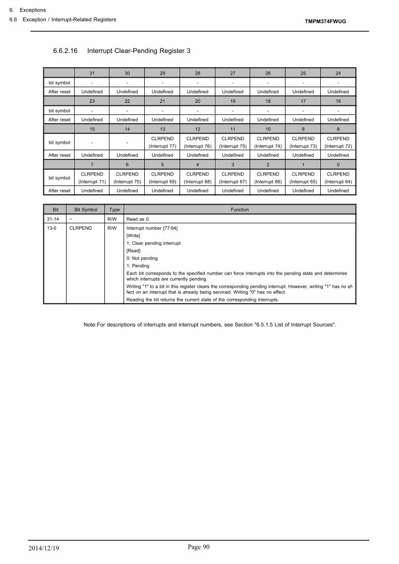
6.6.2.16 Interrupt Clear-Pending Register 3
31 30 29 28 27 26 25 24
bit symbol - - - - - - - -
After reset Undefined Undefined Undefined Undefined Undefined Undefined Undefined Undefined
23 22 21 20 19 18 17 16
bit symbol - - - - - - - -
After reset Undefined Undefined Undefined Undefined Undefined Undefined Undefined Undefined
15 14 13 12 11 10 9 8
bit symbol - -CLRPEND
(Interrupt 77)CLRPEND
(Interrupt 76)CLRPEND
(Interrupt 75)CLRPEND
(Interrupt 74)CLRPEND
(Interrupt 73)CLRPEND
(Interrupt 72)
After reset Undefined Undefined Undefined Undefined Undefined Undefined Undefined Undefined
7 6 5 4 3 2 1 0
bit symbolCLRPEND
(Interrupt 71)CLRPEND
(Interrupt 70)CLRPEND
(Interrupt 69)CLRPEND
(Interrupt 68)CLRPEND
(Interrupt 67)CLRPEND
(Interrupt 66)CLRPEND
(Interrupt 65)CLRPEND
(Interrupt 64)
After reset Undefined Undefined Undefined Undefined Undefined Undefined Undefined Undefined
Bit Bit Symbol Type Function
31-14 − R/W Read as 0.
13-0 CLRPEND R/W Interrupt number [77:64][Write]1: Clear pending interrupt[Read]0: Not pending1: PendingEach bit corresponds to the specified number can force interrupts into the pending state and determineswhich interrupts are currently pending.Writing "1" to a bit in this register clears the corresponding pending interrupt. However, writing "1" has no ef-fect on an interrupt that is already being serviced. Writing "0" has no effect.Reading the bit returns the current state of the corresponding interrupts.
Note:For descriptions of interrupts and interrupt numbers, see Section "6.5.1.5 List of Interrupt Sources".
TMPM374FWUG
6. Exceptions
6.6 Exception / Interrupt-Related Registers
Page 902014/12/19

6.6.2.17 Interrupt Priority Register
Each interrupt is provided with eight bits of an Interrupt Priority Register.
The following shows the addresses of the Interrupt Priority Registers corresponding to interrupt numbers.
31 24 23 16 15 8 7 0
0xE000_E400 − − − −
0xE000_E404 PRI_7 PRI_6 PRI_5 −
0xE000_E408 PRI_11 − PRI_9 PRI_8
0xE000_E40C PRI_15 − PRI_13 −
0xE000_E410 PRI_19 − − −
0xE000_E414 PRI_23 PRI_22 PRI_21 PRI_20
0xE000_E418 PRI_27 PRI_26 PRI_25 PRI_24
0xE000_E41C − PRI_30 PRI_29 −
0xE000_E420 − PRI_34 − PRI_32
0xE000_E424 PRI_39 PRI_38 − PRI_36
0xE000_E428 PRI_43 − − −
0xE000_E42C PRI_47 PRI_46 PRI_45 −
0xE000_E430 PRI_51 PRI_50 PRI_49 PRI_48
0xE000_E434 PRI_55 − PRI_53 PRI_52
0xE000_E438 − − PRI_57 −
0xE000_E43C PRI_63 − − −
0xE000_E440 PRI_67 PRI_66 PRI_65 PRI_64
0xE000_E444 PRI_71 PRI_70 PRI_69 PRI_68
0xE000_E448 PRI_75 PRI_74 PRI_73 PRI_72
0xE000_E44C − − PRI_77 PRI_76
The number of bits to be used for assigning a priority varies with each product. This product uses threebits for assigning a priority.
The following shows the fields of the Interrupt Priority Registers for interrupt numbers 0 to 3. The Inter-rupt Priority Registers for all other interrupt numbers have the identical fields. Unused bits return "0"when read, and writing to unused bits has no effect.
TMPM374FWUG
Page 91 2014/12/19

31 30 29 28 27 26 25 24
bit symbol PRI_3 − − − − −
After reset 0 0 0 0 0 0 0 0
23 22 21 20 19 18 17 16
bit symbol PRI_2 − − − − −
After reset 0 0 0 0 0 0 0 0
15 14 13 12 11 10 9 8
bit symbol PRI_1 − − − − −
After reset 0 0 0 0 0 0 0 0
7 6 5 4 3 2 1 0
bit symbol PRI_0 − − − − −
After reset 0 0 0 0 0 0 0 0
Bit Bit Symbol Type Function
31-29 PRI_3 R/W Priority of interrupt number 3
28-24 − R Read as 0,
23-21 PRI_2 R/W Priority of interrupt number 2
20-16 − R Read as 0,
15-13 PRI_1 R/W Priority of interrupt number 1
12-8 − R Read as 0,
7-5 PRI_0 R/W Priority of interrupt number 0
4-0 − R Read as 0,
TMPM374FWUG
6. Exceptions
6.6 Exception / Interrupt-Related Registers
Page 922014/12/19

6.6.2.18 Vector Table Offset Register
31 30 29 28 27 26 25 24
bit symbol - - TBLBASE TBLOFF
After reset 0 0 0 0 0 0 0 0
23 22 21 20 19 18 17 16
bit symbol TBLOFF
After reset 0 0 0 0 0 0 0 0
15 14 13 12 11 10 9 8
bit symbol TBLOFF
After reset 0 0 0 0 0 0 0 0
7 6 5 4 3 2 1 0
bit symbol TBLOFF - - - - - - -
After reset 0 0 0 0 0 0 0 0
Bit Bit Symbol Type Function
31-30 − R Read as 0,
29 TBLBASE R/W Table baseThe vector table is in:0: Code space1: SRAM space
28-7 TBLOFF R/W Offset valueSet the offset value from the top of the space specified in TBLBASE.The offset must be aligned based on the number of exceptions in the table.This means that the minimumalignment is 32 words that you can use for up to 16 interrupts.For more interrupts, you must adjust the align-ment by rounding up to the next power of two.
6-0 − R Read as 0,
TMPM374FWUG
Page 93 2014/12/19
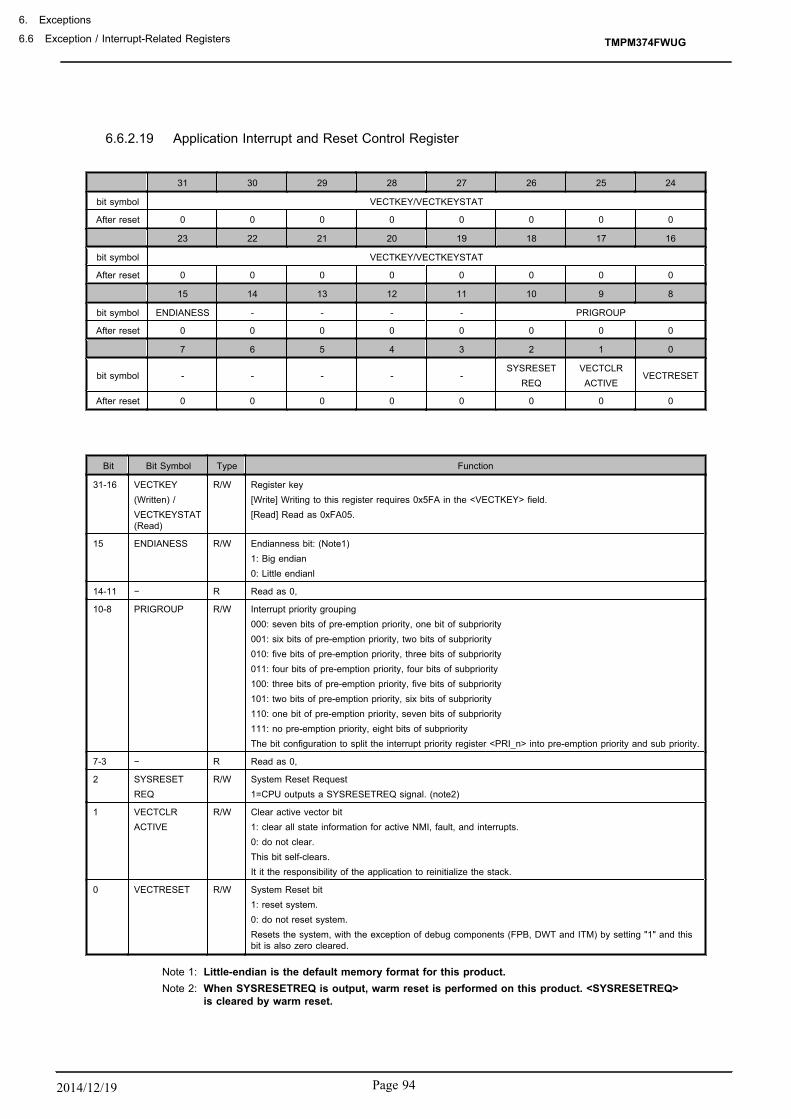
6.6.2.19 Application Interrupt and Reset Control Register
31 30 29 28 27 26 25 24
bit symbol VECTKEY/VECTKEYSTAT
After reset 0 0 0 0 0 0 0 0
23 22 21 20 19 18 17 16
bit symbol VECTKEY/VECTKEYSTAT
After reset 0 0 0 0 0 0 0 0
15 14 13 12 11 10 9 8
bit symbol ENDIANESS - - - - PRIGROUP
After reset 0 0 0 0 0 0 0 0
7 6 5 4 3 2 1 0
bit symbol - - - - -SYSRESET
REQVECTCLRACTIVE
VECTRESET
After reset 0 0 0 0 0 0 0 0
Bit Bit Symbol Type Function
31-16 VECTKEY(Written) /VECTKEYSTAT(Read)
R/W Register key[Write] Writing to this register requires 0x5FA in the <VECTKEY> field.[Read] Read as 0xFA05.
15 ENDIANESS R/W Endianness bit: (Note1)1: Big endian0: Little endianl
14-11 − R Read as 0,
10-8 PRIGROUP R/W Interrupt priority grouping000: seven bits of pre-emption priority, one bit of subpriority001: six bits of pre-emption priority, two bits of subpriority010: five bits of pre-emption priority, three bits of subpriority011: four bits of pre-emption priority, four bits of subpriority100: three bits of pre-emption priority, five bits of subpriority101: two bits of pre-emption priority, six bits of subpriority110: one bit of pre-emption priority, seven bits of subpriority111: no pre-emption priority, eight bits of subpriorityThe bit configuration to split the interrupt priority register <PRI_n> into pre-emption priority and sub priority.
7-3 − R Read as 0,
2 SYSRESETREQ
R/W System Reset Request1=CPU outputs a SYSRESETREQ signal. (note2)
1 VECTCLRACTIVE
R/W Clear active vector bit1: clear all state information for active NMI, fault, and interrupts.0: do not clear.This bit self-clears.It it the responsibility of the application to reinitialize the stack.
0 VECTRESET R/W System Reset bit1: reset system.0: do not reset system.Resets the system, with the exception of debug components (FPB, DWT and ITM) by setting "1" and thisbit is also zero cleared.
Note 1: Little-endian is the default memory format for this product.Note 2: When SYSRESETREQ is output, warm reset is performed on this product. <SYSRESETREQ>
is cleared by warm reset.
TMPM374FWUG
6. Exceptions
6.6 Exception / Interrupt-Related Registers
Page 942014/12/19
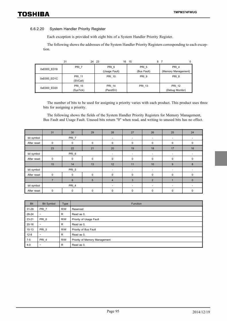
6.6.2.20 System Handler Priority Register
Each exception is provided with eight bits of a System Handler Priority Register.
The following shows the addresses of the System Handler Priority Registers corresponding to each excep-tion.
31 24 23 16 15 8 7 0
0xE000_ED18PRI_7
PRI_6
(Usage Fault)PRI_5
(Bus Fault)PRI_4
(Memory Management)
0xE000_ED1CPRI_11(SVCall)
PRI_10
PRI_9
PRI_8
0xE000_ED20PRI_15
(SysTick)PRI_14
(PendSV)PRI_13
PRI_12
(Debug Monitor)
The number of bits to be used for assigning a priority varies with each product. This product uses threebits for assigning a priority.
The following shows the fields of the System Handler Priority Registers for Memory Management,Bus Fault and Usage Fault. Unused bits return "0" when read, and writing to unused bits has no effect.
31 30 29 28 27 26 25 24
bit symbol PRI_7 - - - - -
After reset 0 0 0 0 0 0 0 0
23 22 21 20 19 18 17 16
bit symbol PRI_6 - - - - -
After reset 0 0 0 0 0 0 0 0
15 14 13 12 11 10 9 8
bit symbol PRI_5 - - - - -
After reset 0 0 0 0 0 0 0 0
7 6 5 4 3 2 1 0
bit symbol PRI_4 - - - - -
After reset 0 0 0 0 0 0 0 0
Bit Bit Symbol Type Function
31-29 PRI_7 R/W Reserved
28-24 − R Read as 0,
23-21 PRI_6 R/W Priority of Usage Fault
20-16 − R Read as 0,
15-13 PRI_5 R/W Priority of Bus Fault
12-8 − R Read as 0,
7-5 PRI_4 R/W Priority of Memory Management
4-0 − R Read as 0,
TMPM374FWUG
Page 95 2014/12/19

6.6.2.21 System Handler Control and State Register
31 30 29 28 27 26 25 24
bit symbol - - - - - - - -
After reset 0 0 0 0 0 0 0 0
23 22 21 20 19 18 17 16
bit symbol - - - - -USGFAULT
ENABUSFAULT
ENAMEMFAULT
ENA
After reset 0 0 0 0 0 0 0 0
15 14 13 12 11 10 9 8
bit symbolSVCALLPENDED
BUSFAULTPENDED
MEMFAULTPENDED
USGFAULTPENDED
SYSTICKACT PENDSVACT -MONITOR
ACT
After reset 0 0 0 0 0 0 0 0
7 6 5 4 3 2 1 0
bit symbol SVCALLACT - - -USGFAULT
ACT-
BUSFAULTACT
MEMFAULTACT
After reset 0 0 0 0 0 0 0 0
Bit Bit Symbol Type Function
31-19 − R Read as 0,
18 USGFAULTENA
R/W Usage Fault0: Disabled1: Enabled
17 BUSFAULTENA
R/W Bus Fault0: Disable1: Enable
16 MEMFAULTENA
R/W Memory Management0: Disable1: Enable
15 SVCALLPENDED
R/W SVCall0: Not pended1: Pended
14 BUSFAULTPENDED
R/W Bus Fault0: Not pended1: Pended
13 MEMFAULTPENDED
R/W Memory Management0: Not pended1: Pended
12 USGFAULTPENDED
R/W Usage Fault0: Not pended1: Pended
11 SYSTICKACT R/W SysTick0: Inactive1: Active
10 PENDSVACT R/W PendSV0: Inactive1: Active
9 − R Read as 0,
8 MONITORACT R/W Debug monitor0: Inactive1: Active
7 SVCALLACT R/W SVCall0: Inactive1: Active
6-4 − R Read as 0,
TMPM374FWUG
6. Exceptions
6.6 Exception / Interrupt-Related Registers
Page 962014/12/19

Bit Bit Symbol Type Function
3 USGFAULTACT
R/W Usage Fault0: Inactive1: Active
2 − R Read as 0,
1 BUSFAULTACT
R/W Bus Fault0: Inactive1: Active
0 MEMFAULTACT
R/W Memory management0: Inactive1: Active
Note:You must clear or set the active bits with extreme caution because clearing and setting these bits does not re-pair stack contents.
TMPM374FWUG
Page 97 2014/12/19

6.6.3 Clock generator registers
Be sure to set the active level of the release request when an interrupt is enabled for releasing STOP/IDLEmode.
1. When using interrupts, be sure to follow the sequence of actions shown below:a. If the external intrrupt request pin shared with other general ports, enable the port to receive
the interrupt.b. Set the conditions including the active state at the initial state.c. Clear interrupt requests.d. Enable interrupts.
2. Each setting must be performed while the interrupts are disabled.
3. In the TMPM374, seven factors (INT5 to INT7 and INT9 to INTF) are available as the release fac-tors. Registers in the CG are used for selecting edge/level of active state and for specifying the inter-rupt to release STOP/IDLE mode.
4. If INT5 to INT7 and INT9 to INTF, which are used to release STOP/IDLE mode, are used as the nor-mal interrupts, the setting of the CG is not necessarily required.
TMPM374FWUG
6. Exceptions
6.6 Exception / Interrupt-Related Registers
Page 982014/12/19
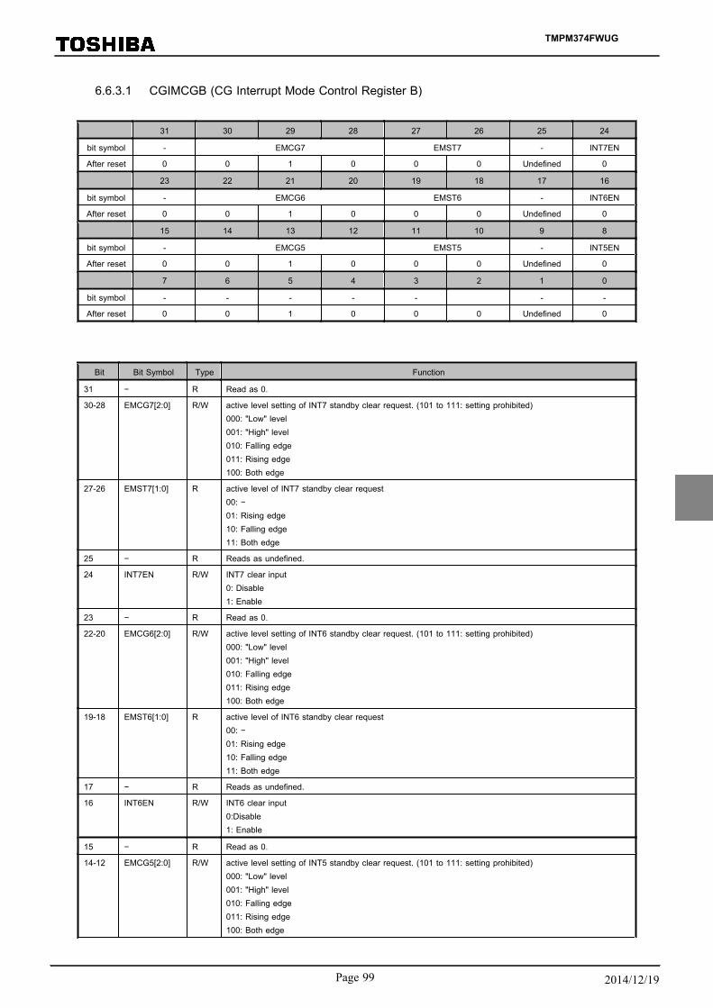
6.6.3.1 CGIMCGB (CG Interrupt Mode Control Register B)
31 30 29 28 27 26 25 24
bit symbol - EMCG7 EMST7 - INT7EN
After reset 0 0 1 0 0 0 Undefined 0
23 22 21 20 19 18 17 16
bit symbol - EMCG6 EMST6 - INT6EN
After reset 0 0 1 0 0 0 Undefined 0
15 14 13 12 11 10 9 8
bit symbol - EMCG5 EMST5 - INT5EN
After reset 0 0 1 0 0 0 Undefined 0
7 6 5 4 3 2 1 0
bit symbol - - - - - - -
After reset 0 0 1 0 0 0 Undefined 0
Bit Bit Symbol Type Function
31 − R Read as 0.
30-28 EMCG7[2:0] R/W active level setting of INT7 standby clear request. (101 to 111: setting prohibited)000: "Low" level001: "High" level010: Falling edge011: Rising edge100: Both edge
27-26 EMST7[1:0] R active level of INT7 standby clear request00: −01: Rising edge10: Falling edge11: Both edge
25 − R Reads as undefined.
24 INT7EN R/W INT7 clear input0: Disable1: Enable
23 − R Read as 0.
22-20 EMCG6[2:0] R/W active level setting of INT6 standby clear request. (101 to 111: setting prohibited)000: "Low" level001: "High" level010: Falling edge011: Rising edge100: Both edge
19-18 EMST6[1:0] R active level of INT6 standby clear request00: −01: Rising edge10: Falling edge11: Both edge
17 − R Reads as undefined.
16 INT6EN R/W INT6 clear input0:Disable1: Enable
15 − R Read as 0.
14-12 EMCG5[2:0] R/W active level setting of INT5 standby clear request. (101 to 111: setting prohibited)000: "Low" level001: "High" level010: Falling edge011: Rising edge100: Both edge
TMPM374FWUG
Page 99 2014/12/19

Bit Bit Symbol Type Function
11-10 EMST5[1:0] R active level of INT5 standby clear request00: −01: Rising edge10: Falling edge11: Both edge
9 − R Reads as undefined.
8 INT5EN R/W INT5 clear input0: Disable1: Enable
7 − R Read as 0.
6-4 − R/W Write optional value.
3-2 − R Read as 0.
1 − R Read as undefined.
0 − R/W Write as 0.
Note 1: <EMSTx> is effective only when <EMCGx[2:0]> is set to "100" for both rising and falling edge. The active level usedfor the reset of standby can be checked by referring <EMSTx>. If interrupts are cleared with the CGICRCG register,<EMSTx> is also cleared.
Note 2: Please specify the bit for the edge first and then specify the bit for the <INTxEN>. Setting them simultaneously is pro-hibited.
TMPM374FWUG
6. Exceptions
6.6 Exception / Interrupt-Related Registers
Page 1002014/12/19

6.6.3.2 CGIMCGD (CG Interrupt Mode Control Register D)
31 30 29 28 27 26 25 24
bit symbol - EMCGF EMSTF - INTFEN
After reset 0 0 1 0 0 0 Undefined 0
23 22 21 20 19 18 17 16
bit symbol - EMCGE EMSTE - INTEEN
After reset 0 0 1 0 0 0 Undefined 0
15 14 13 12 11 10 9 8
bit symbol - EMCGD EMSTD - INTDEN
After reset 0 0 1 0 0 0 Undefined 0
7 6 5 4 3 2 1 0
bit symbol - EMCGC EMSTC - INTCEN
After reset 0 0 1 0 0 0 Undefined 0
Bit Bit Symbol Type Function
31 − R Read as 0.
30-28 EMCGF[2:0] R/W active level setting of INTF standby clear request. (101 to 111: setting prohibited)000: "Low" level001: "High" level010: Falling edge011: Rising edge100: Both edge
27-26 EMSTF[1:0] R active level of INTF standby clear request00: −01: Rising edge10: Falling edge11: Both edge
25 − R Reads as undefined.
24 INTFEN R/W INTF clear input0: Disable1: Enable
23 − R Read as 0.
22-20 EMCGE[2:0] R/W active level setting of INTE standby clear request. (101 to 111: setting prohibited)000: "Low" level001: "High" level010: Falling edge011: Rising edge100: Both edge
19-18 EMSTE[1:0] R active level of INTE standby clear request00: −01: Rising edge10: Falling edge11: Both edge
17 − R Reads as undefined.
16 INTEEN R/W INTE clear input0: Disable1: Enable
15 − R Read as 0.
14-12 EMCGD[2:0] R/W active level setting of INTD standby clear request. (101 to 111: setting prohibited)000: "Low" level001: "High" level010: Falling edge011: Rising edge100: Both edge
TMPM374FWUG
Page 101 2014/12/19

Bit Bit Symbol Type Function
11-10 EMSTD[1:0] R active level of INTD standby clear request00: −01: Rising edge10: Falling edge11: Both edge
9 − R Reads as undefined.
8 INTDEN R/W INTD clear input0: Disable1: Enable
7 − R Read as 0.
6-4 EMCGC[2:0] R/W active level setting of INTC standby clear request. (101 to 111: setting prohibited)000: "Low" level001: "High" level010: Falling edge011: Rising edge100: Both edge
3-2 EMSTC[1:0] R active level of INTC standby clear request00: −01: Rising edge10: Falling edge11: Both edge
1 − R Reads as undefined.
0 INTCEN R/W INTC clear input0: Disable1: Enable
Note 1: <EMSTx> is effective only when <EMCGx[2:0]> is set to "100" for both rising and falling edge. The active level usedfor the reset of standby can be checked by referring <EMSTx>. If interrupts are cleared with the CGICRCG register,<EMSTx> is also cleared.
Note 2: Please specify the bit for the edge first and then specify the bit for the <INTxEN>. Setting them simultaneously is pro-hibited.
TMPM374FWUG
6. Exceptions
6.6 Exception / Interrupt-Related Registers
Page 1022014/12/19

6.6.3.3 CGICRCG (CG Interrupt Request Clear Register)
31 30 29 28 27 26 25 24
bit symbol - - - - - - - -
After reset 0 0 0 0 0 0 0 0
23 22 21 20 19 18 17 16
bit symbol - - - - - - - -
After reset 0 0 0 0 0 0 0 0
15 14 13 12 11 10 9 8
bit symbol - - - - - - - -
After reset 0 0 0 0 0 0 0 0
7 6 5 4 3 2 1 0
bit symbol - - - ICRCG
After reset 0 0 0 0 0 0 0 0
Bit Bit Symbol Type Function
31-5 − R Read as 0,
4-0 ICRCG[4:0] W Clear interrupt requests.
0_0000:Reserved 0_1000: Reserved
0_0001: Reserved 0_1001: Reserved
0_0010: Reserved 0_1010:Reserved
0_0011: Reserved 0_1011: Reserved
0_0100: Reserved 0_1100:INTC
0_0101: INT5 0_1101: INTD
0_0110: INT6 0_1110: INTE
0_ 0111: INT7 0_1111: INTF 1_0000 to 1_1111: Reserved
Read as 0.
TMPM374FWUG
Page 103 2014/12/19

6.6.3.4 CGNMIFLG (NMI Flag Register)
31 30 29 28 27 26 25 24
bit symbol - - - - - - - -
After reset 0 0 0 0 0 0 0 0
23 22 21 20 19 18 17 16
bit symbol - - - - - - - -
After reset 0 0 0 0 0 0 0 0
15 14 13 12 11 10 9 8
bit symbol - - - - - - - -
After reset 0 0 0 0 0 0 0 0
7 6 5 4 3 2 1 0
bit symbol - - - - - - - NMIFLG0
After reset 0 0 0 0 0 0 0 0
Bit Bit Symbol Type Function
31-1 − R Read as 0.
0 NMIFLG0 R NMI source generation flag0: not applicable1: generated from WDT
Note:<NMIFLG> are cleared to "0" when they are read.
TMPM374FWUG
6. Exceptions
6.6 Exception / Interrupt-Related Registers
Page 1042014/12/19

6.6.3.5 CGRSTFLG (Reset Flag Register)
31 30 29 28 27 26 25 24
bit symbol - - - - - - - -
After Power-onreset 0 0 0 0 0 0 0 0
23 22 21 20 19 18 17 16
bit symbol - - - - - - - -
After Power-onreset 0 0 0 0 0 0 0 0
15 14 13 12 11 10 9 8
bit symbol - - - - - - - -
After Power-onreset 0 0 0 0 0 0 0 0
7 6 5 4 3 2 1 0
bit symbol - - OFDRSTF DBGRSTF VLTDRSTF WDTRSTF PINRSTF PONRSTF
After Power-onreset 0 0 0 0 0 0 0 1
Bit Bit Symbol Type Function
31-6 − R Read as 0.
5 OFDRSTF R/W OFD reset flag (Note1)0: "0" is written1: Reset from OFD
4 DBGRSTF R/W Debug reset flag (Note1)0: "0" is written1: Reset from SYSRESETREQ
3 VLTDRSTF R/W VLTD reset flag0: "0" is written1: Reset from VLTD
2 WDTRSTF R/W WDT reset flag0: "0" is written1: Reset from WDT
1 PINRSTF R/W RESET pin flag0: "0" is written1: Reset from RESET pin
0 PONRSTF R/W Power-on flag0: "0" is written1: Reset from power-on reset
Note 1: This flag indicates a reset generated by the SYSRESETREQ bit of the Application Interrupt and Reset Control Regis-ter of the CPU's NVIC.
Note 2: This product has power-on reset circuit and this register is initialized only by power-on reset. Therefore, "1" is set tothe <PONRSTF> bit in initial reset state right after power-on. Note that this bit is not set by the second and subse-quent resets and this register is not cleared automatically. Write "0" to clear the register.
TMPM374FWUG
Page 105 2014/12/19

TMPM374FWUG
6. Exceptions
6.6 Exception / Interrupt-Related Registers
Page 1062014/12/19

7. Internal High-speed Oscillation Adjustment Function
TMPM374FWUG has the internal high-speed oscillation adjustment function.
Note:This adjustment function is not applicable to the reference clock for OFD.
7.1 StructureThe internal oscillation adjustment function uses the pulse width measurement function of 16-bit timer/event coun-
ter (TMRB).
Figure 7-1 shows the function configuration.
CPU TMRB
InternalHigh-speedOscillator
TRMOSCINIT
TRMOSCSET
TRMOSCEN
clockInitial vaiueread
Trimming dataset
Capture Interrupt
TBxIN
Figure 7-1 Function block diagram
TMPM374FWUG
Page 107 2014/12/19

7.2 Registers
7.2.1 Register list
The control registers and its addresses are as follows.
Base Address = 0x4004 _ 0300
Register name Address(Base+)
Protect register TRMOSCPRO 0x0000
Enable register TRMOSCEN 0x0004
Initial trimming value monitoring register TRMOSCINIT 0x0008
Trimming value setting register TRMOSCSET 0x000C
7.2.2 TRMOSCPRO (Protect register)
31 30 29 28 27 26 25 24
bit symbol - - - - - - - -
After reset 0 0 0 0 0 0 0 0
23 22 21 20 19 18 17 16
bit symbol - - - - - - - -
After reset 0 0 0 0 0 0 0 0
15 14 13 12 11 10 9 8
bit symbol - - - - - - - -
After reset 0 0 0 0 0 0 0 0
7 6 5 4 3 2 1 0
bit symbol PROTECT
After reset 0 0 0 0 0 0 0 0
Bit Bit Symbol Type Function
31-8 − R Read as "0".
7-0 PROTECT[7:0] R/W Writing register control0xC1 : EnableOther than 0xC1 : DesableWhen "0xC1" is set, TRMOSCEN, TRMOSCINIT and TRMOSCSET are allowed to write.
TMPM374FWUG
7. Internal High-speed Oscillation Adjustment Function
7.2 Registers
Page 1082014/12/19

7.2.3 TRMOSCEN (Enable register)
31 30 29 28 27 26 25 24
bit symbol - - - - - - - -
After reset 0 0 0 0 0 0 0 0
23 22 21 20 19 18 17 16
bit symbol - - - - - - - -
After reset 0 0 0 0 0 0 0 0
15 14 13 12 11 10 9 8
bit symbol - - - - - - - -
After reset 0 0 0 0 0 0 0 0
7 6 5 4 3 2 1 0
bit symbol - - - - - - - TRIMEN
After reset 0 0 0 0 0 0 0 0
Bit Bit Symbol Type Function
31-1 − R Read as "0".
0 TRIMEN R/W Trimming control0 : Disable1 : EnableWhen "1" is set, a trimming value of the internal oscillator is switched from a value of TRIMOSCINIT to a val-ue of TRMOSCSET.
TMPM374FWUG
Page 109 2014/12/19

7.2.4 TRMOSCINIT (Initial trimming value monitor register)
31 30 29 28 27 26 25 24
bit symbol - - - - - - - -
After reset 0 0 0 0 0 0 0 0
23 22 21 20 19 18 17 16
bit symbol - - - - - - - -
After reset 0 0 0 0 0 0 0 0
15 14 13 12 11 10 9 8
bit symbol - - TRIMINITC
After reset 0 0 Undifined
7 6 5 4 3 2 1 0
bit symbol - - - - TRIMINITF
After reset 0 0 0 0 Undefined
Bit Bit Symbol Type Function
31-14 − R Read as "0".
13-8 TRIMINITC[5:0]
R/W Initial coarse trimming valueEnables to monitor initial coarse trimming value.
7-4 − R Read as "0".
3-0 TRIMINITF[3:0] R/W Initial fine trimming valueEnables to monitor initial fine trimming value.
For details about the specific setting and adjustment value of coarse trimming and fine trimming, refer to "Ta-ble 7-1 Adjustment range".
TMPM374FWUG
7. Internal High-speed Oscillation Adjustment Function
7.2 Registers
Page 1102014/12/19

7.2.5 TRMOSCSET (Trimming value setting register)
31 30 29 28 27 26 25 24
bit symbol - - - - - - - -
After reset 0 0 0 0 0 0 0 0
23 22 21 20 19 18 17 16
bit symbol - - - - - - - -
After reset 0 0 0 0 0 0 0 0
15 14 13 12 11 10 9 8
bit symbol - - TRIMSETC
After reset 0 0 0 0 0 0 0 0
7 6 5 4 3 2 1 0
bit symbol - - - - TRIMSETF
After reset 0 0 0 0 0 0 0 0
Bit Bit Symbol Type Function
31-14 − R Read as "0".
13-8 TRIMSETC[5:0]
R/W Coarse trimming value settingSets the coarse trimming value.
7-4 − R Read as "0".
3-0 TRIMSETF[4:0] R/W Fine trimming value settingSets the fine trimming value.
For details about the specific setting and adjustment value of coarse trimming and fine trimming, refer to "Ta-ble 7-1 Adjustment range".
TMPM374FWUG
Page 111 2014/12/19

7.3 Operational Description
7.3.1 Outline
Oscillation is adjusted using coarse trimming values and fine trimming values.
The value setting before shipping can be checked with TRMOSCINIT<TRIMINITC> and <TRIMINITF>.When the value changing, set a new value to TRMOSCSET<TRIMSETC> and <TRIMSETF>. By setting"1" to TRMOSCEN<TRIMEN>, a setting value of the internal oscillator will be changed.
Note:After reset, writing to TRMOSCSET and TRMOSCEN is prohibited. When writing to these bits,TRMOSCPRO<PROTECT> must be set to "0xC1".
7.3.2 Adjustment range
In the coarse trimming, −57.6% to +55.8% adjustment by 1.8%-step is feasible. In the fine trimming,−2.4% to +2.1% adjustment by 0.3%-step is feasible. Table 7-1 shows a adjustment range.
Note:Each step value is assumed based on the typical condition. In the coarse trimming, it has ±0.2% mar-gin of error. In the fine trimming, it has ±0.1% margin of error.
Table 7-1 Adjustment range
Coarse trimming Fine trimming
<TRIMSETC>Frequency
change(typ.)
<TRIMSETF>Frequency
change(typ.)
011111 +55.8% 0111 +2.1%
・ ・ ・ ・
000001 +1.8% 0001 +0.3%
000000 ±0% 0000 ±0%
111111 −1.8% 1111 −0.3%
111110 −3.6% 1110 −0.6%
・ ・ ・ ・
100000 −57.6% 1000 −2.4%
7.3.3 Internal Oscillation Frequency Measurement using TMRB
To measure a frequency of high-speed oscillator, the pulse width measurement function of TMRB can beused. First, choose an internal oscillator as a prescaler clock ΦT0 of TMRB. Second, input a pulse fromTBxIN. Third, capture an up-counter value at the rising edge of the pulse using the capture function. Finally,determine the adjustment value using a difference between a frequency of TBxIN calculated with capture val-ue and the actual frequency.
TMPM374FWUG
7. Internal High-speed Oscillation Adjustment Function
7.3 Operational Description
Page 1122014/12/19

8. Input / Output Ports
8.1 Port Functions
8.1.1 Function list
TMPM374FWUG has 33 ports. Besides the ports function, these ports can be used as I/O pins for peripher-al functions.
Table 8-1 shows the port function table.
Table 8-1 Port Function List
Port PIn Input /Out-put
Pull-upPull-down
SchmittInput
Noise FilterProgram-
mableOpen-drain
Function pin
PORTA
PA4 I/O Pull-up / Pull-down ο - ο SCLK1 , CTS1
PA5 I/O Pull-up / Pull-down ο - ο TXD1 , TB6OUT
PA6 I/O Pull-up / Pull-down ο - ο RXD1 , TB6IN
PORTB
PB3 I/O Pull-up / Pull-down ο - ο TMS / SWDIO
PB4 I/O Pull-up / Pull-down ο - ο TCK / SWCLK
PB5 I/O Pull-up / Pull-down ο - ο TDO / SWV
PB6 I/O Pull-up / Pull-down ο - ο TDI
PORTE
PE0 I/O Pull-up / Pull-down ο - ο TXD0
PE1 I/O Pull-up / Pull-down ο - ο RXD0
PE2 I/O Pull-up / Pull-down ο - ο SCLK0 , CTS0
PE4 I/O Pull-up / Pull-down ο ο ο TB2IN , INT5
PE6 I/O Pull-up / Pull-down ο ο ο TB3IN , INT6
PE7 I/O Pull-up / Pull-down ο ο ο TB3OUT , INT7
PORTF
PF0 I/O Pull-up / Pull-down ο - ο TB7IN , BOOT
PF2 I/O Pull-up / Pull-down ο - ο ENCA1 , SCLK3 , CTS3
PF3 I/O Pull-up / Pull-down ο - ο ENCB1 , TXD3
PF4 I/O Pull-up / Pull-down ο - ο ENCZ1 , RXD3
PORTG
PG0 I/O Pull-up / Pull-down ο - ο UO1
PG1 I/O Pull-up / Pull-down ο - ο XO1
PG2 I/O Pull-up / Pull-down ο - ο VO1
PG3 I/O Pull-up / Pull-down ο - ο YO1
PG4 I/O Pull-up / Pull-down ο - ο WO1
PG5 I/O Pull-up / Pull-down ο - ο ZO1
PG6 I/O Pull-up / Pull-down ο - ο EMG1
PG7 I/O Pull-up / Pull-down ο - ο OVV1
PORTI
PI3 I/O Pull-up / Pull-down ο - ο AINB2
ο : Exist- : Not Exist
TMPM374FWUG
Page 113 2014/12/19

Table 8-1 Port Function List
Port PIn Input /Out-put
Pull-upPull-down
SchmittInput
Noise FilterProgram-
mableOpen-drain
Function pin
PORTJ
PJ0 I/O Pull-up / Pull-down ο - ο AINB3
PJ6 I/O Pull-up / Pull-down ο ο ο INTC , AINB9
PJ7 I/O Pull-up / Pull-down ο ο ο INTD , AINB10
PORTK
PK0 I/O Pull-up / Pull-down ο ο ο INTE , AINB11
PK1 I/O Pull-up / Pull-down ο ο ο INTF , AINB12
PORTM
PM0 I/O Pull-up / Pull-down ο - ο X1
PM1 I/O Pull-up / Pull-down ο - ο X2
ο : Exist- : Not Exist
Note:The noise elimination width of the noise filter is approximately 30 ns under typical conditions.
TMPM374FWUG
8. Input / Output Ports
8.1 Port Functions
Page 1142014/12/19

8.1.2 Port Registers Outline
The following registers need to be configured to use ports.
・ PxDATA: Port x data register
To read / write port data.
・ PxCR: Port x output control register
To control output.
PxIE needs to be configured to control input.
・ PxFRn: Port x function register n
To set function.
An assigned function can be activated by setting "1".
・ PxOD: Port x open drain control register
To control the programmable open drain.
Programmable open drain is function to be materialized pseudo-open-drain by setting the PxOD.
When PxOD is set "1",output buffer is disabled and pseudo-open-drain is materialized.
・ PxPUP: Port x pull-up control register
To control programmable pull ups.
・ PxPDN: Port x pull-down control register
To control programmable pull downs.
・ PxIE:Port x input control register
To control inputs.
For avoided through current, default setting prohibits inputs.
TMPM374FWUG
Page 115 2014/12/19

8.1.3 Port States in STOP Mode
Input and output in STOP mode are enabled / disabled by the CGSTBYCR<DRVE> bit.
If PxIE or PxCR is enabled with <DRVE>=1, input or output is enabled respectively in STOP mode.If<DRVE>=0, both input and output are disabled in STOP mode except for some ports even if PxIE orPxCR are enabled.
Table 8-2 shows the pin conditions in STOP mode.
Table 8-2 Port conditions in STOP mode
Pin name I/O <DRVE> = 0 <DRVE> = 1
Not port RESET, MODE Input only ο
Port
X1 Input only ×
X2 Output only "High" level output
TMSTCKTDI
Input ο
TDO OutputEnabled when data is valid.
Disabled when data is invalid.
SWCLK Input ο
SWDIO
Input ο
OutputEnabled when data is valid.
Disabled when data is invalid.
SWV Output ο
UO1VO1WO1XO1YO1ZO1
OutputEnabled when data is valid.
Disabled when data is invalid.
INT5INT6, INT7INTC, INTD, INTEINTF
Input ο
Other function pins otherthan the above or theports that are used as gen-eral purpose ports.
Input × ο
Output × ο
ο : Input or output enabled.× : Input or output disabled.
TMPM374FWUG
8. Input / Output Ports
8.1 Port Functions
Page 1162014/12/19
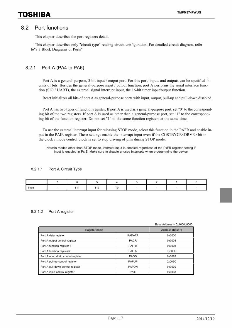
8.2 Port functionsThis chapter describes the port registers detail.
This chapter describes only "circuit type" reading circuit configuration. For detailed circuit diagram, referto"8.3 Block Diagrams of Ports".
8.2.1 Port A (PA4 to PA6)
Port A is a general-purpose, 3-bit input / output port. For this port, inputs and outputs can be specified inunits of bits. Besides the general-purpose input / output function, port A performs the serial interface func-tion (SIO / UART), the external signal interrupt input, the 16-bit timer input/output function.
Reset initializes all bits of port A as general-purpose ports with input, output, pull-up and pull-down disabled.
Port A has two types of function register. If port A is used as a general-purpose port, set "0" to the correspond-ing bit of the two registers. If port A is used as other than a general-purpose port, set "1" to the correspond-ing bit of the function register. Do not set "1" to the some function registers at the same time.
To use the external interrupt input for releasing STOP mode, select this function in the PAFR and enable in-put in the PAIE register. These settings enable the interrupt input even if the CGSTBYCR<DRVE> bit inthe clock / mode control block is set to stop driving of pins during STOP mode.
Note:In modes other than STOP mode, interrupt input is enabled regardless of the PxFR register setting ifinput is enabled in PxIE. Make sure to disable unused interrupts when programming the device.
8.2.1.1 Port A Circuit Type
7 6 5 4 3 2 1 0
Type - T11 T13 T9 - - - -
8.2.1.2 Port A register
Base Address = 0x4000_0000
Register name Address (Base+)
Port A data register PADATA 0x0000
Port A output control register PACR 0x0004
Port A function register 1 PAFR1 0x0008
Port A function register2 PAFR2 0x000C
Port A open drain control register PAOD 0x0028
Port A pull-up control register PAPUP 0x002C
Port A pull-down control register PAPDN 0x0030
Port A input control register PAIE 0x0038
TMPM374FWUG
Page 117 2014/12/19

8.2.1.3 PADATA (Port A data register)
31 30 29 28 27 26 25 24
bit symbol - - - - - - - -
After reset 0 0 0 0 0 0 0 0
23 22 21 20 19 18 17 16
bit symbol - - - - - - - -
After reset 0 0 0 0 0 0 0 0
15 14 13 12 11 10 9 8
bit symbol - - - - - - - -
After reset 0 0 0 0 0 0 0 0
7 6 5 4 3 2 1 0
bit symbol - PA6 PA5 PA4 - - - -
After reset 0 0 0 0 0 0 0 0
Bit Bit Symbol Type Function
31-8 − R Read as 0.
7 − R/W Write 0.
6-4 PA6 to PA4 R/W Port A data register
3-0 − R/W Write 0.
TMPM374FWUG
8. Input / Output Ports
8.2 Port functions
Page 1182014/12/19

8.2.1.4 PACR (Port A output control register)
31 30 29 28 27 26 25 24
bit symbol - - - - - - - -
After reset 0 0 0 0 0 0 0 0
23 22 21 20 19 18 17 16
bit symbol - - - - - - - -
After reset 0 0 0 0 0 0 0 0
15 14 13 12 11 10 9 8
bit symbol - - - - - - - -
After reset 0 0 0 0 0 0 0 0
7 6 5 4 3 2 1 0
bit symbol - PA6C PA5C PA4C - - - -
After reset 0 0 0 0 0 0 0 0
Bit Bit Symbol Type Function
31-8 − R Read as 0.
7 − R/W Write 0.
6-4 PA6C to PA4C R/W Output0: Disable1: Enable
3-0 − R/W Write 0.
TMPM374FWUG
Page 119 2014/12/19

8.2.1.5 PAFR1 (Port A function register 1)
31 30 29 28 27 26 25 24
bit symbol - - - - - - - -
After reset 0 0 0 0 0 0 0 0
23 22 21 20 19 18 17 16
bit symbol - - - - - - - -
After reset 0 0 0 0 0 0 0 0
15 14 13 12 11 10 9 8
bit symbol - - - - - - - -
After reset 0 0 0 0 0 0 0 0
7 6 5 4 3 2 1 0
bit symbol - PA6F1 PA5F1 PA4F1 - - - -
After reset 0 0 0 0 0 0 0 0
Bit Bit Symbol Type Function
31-8 − R Read as 0.
7 − R/W Write 0.
6 PA6F1 R/W 0: PORT1: RXD1
5 PA5F1 R/W 0: PORT1: TXD1
4 PA4F1 R/W 0: PORT1: SCLK1
3-0 − R/W Write 0.
TMPM374FWUG
8. Input / Output Ports
8.2 Port functions
Page 1202014/12/19

8.2.1.6 PAFR2 (Port A function register 2)
31 30 29 28 27 26 25 24
bit symbol - - - - - - - -
After reset 0 0 0 0 0 0 0 0
23 22 21 20 19 18 17 16
bit symbol - - - - - - - -
After reset 0 0 0 0 0 0 0 0
15 14 13 12 11 10 9 8
bit symbol - - - - - - - -
After reset 0 0 0 0 0 0 0 0
7 6 5 4 3 2 1 0
bit symbol - PA6F2 PA5F2 PA4F2 - - - -
After reset 0 0 0 0 0 0 0 0
Bit Bit Symbol Type Function
31-8 − R Read as 0.
7 − R/W Write "0".
6 PA6F2 R/W 0: PORT1: TB6IN
5 PA5F2 R/W 0: PORT1: TB6OUT
4 PA4F2 R/W 0: PORT1: CTS1
3-0 − R Read as 0.
TMPM374FWUG
Page 121 2014/12/19

8.2.1.7 PAOD (Port A open drain control register)
31 30 29 28 27 26 25 24
bit symbol - - - - - - - -
After reset 0 0 0 0 0 0 0 0
23 22 21 20 19 18 17 16
bit symbol - - - - - - - -
After reset 0 0 0 0 0 0 0 0
15 14 13 12 11 10 9 8
bit symbol - - - - - - - -
After reset 0 0 0 0 0 0 0 0
7 6 5 4 3 2 1 0
bit symbol - PA6OD PA5OD PA4OD - - - -
After reset 0 0 0 0 0 0 0 0
Bit Bit Symbol Type Function
31-8 − R Read as 0.
7 − R/W Write "0".
6-4 PA6OD toPA4OD
R/W 0 : CMOS1 : Open-drain
3-0 − R/W Write "0".
TMPM374FWUG
8. Input / Output Ports
8.2 Port functions
Page 1222014/12/19

8.2.1.8 PAPUP (Port A pull-up control register)
31 30 29 28 27 26 25 24
bit symbol - - - - - - - -
After reset 0 0 0 0 0 0 0 0
23 22 21 20 19 18 17 16
bit symbol - - - - - - - -
After reset 0 0 0 0 0 0 0 0
15 14 13 12 11 10 9 8
bit symbol - - - - - - - -
After reset 0 0 0 0 0 0 0 0
7 6 5 4 3 2 1 0
bit symbol - PA6UP PA5UP PA4UP - - - -
After reset 0 0 0 0 0 0 0 0
Bit Bit Symbol Type Function
31-8 − R Read as 0.
7 − R/W Write "0".
6-4 PA6UP toPA4UP
R/W Pull-up0: Disable1: Enable
3-0 − R/W Write "0".
TMPM374FWUG
Page 123 2014/12/19
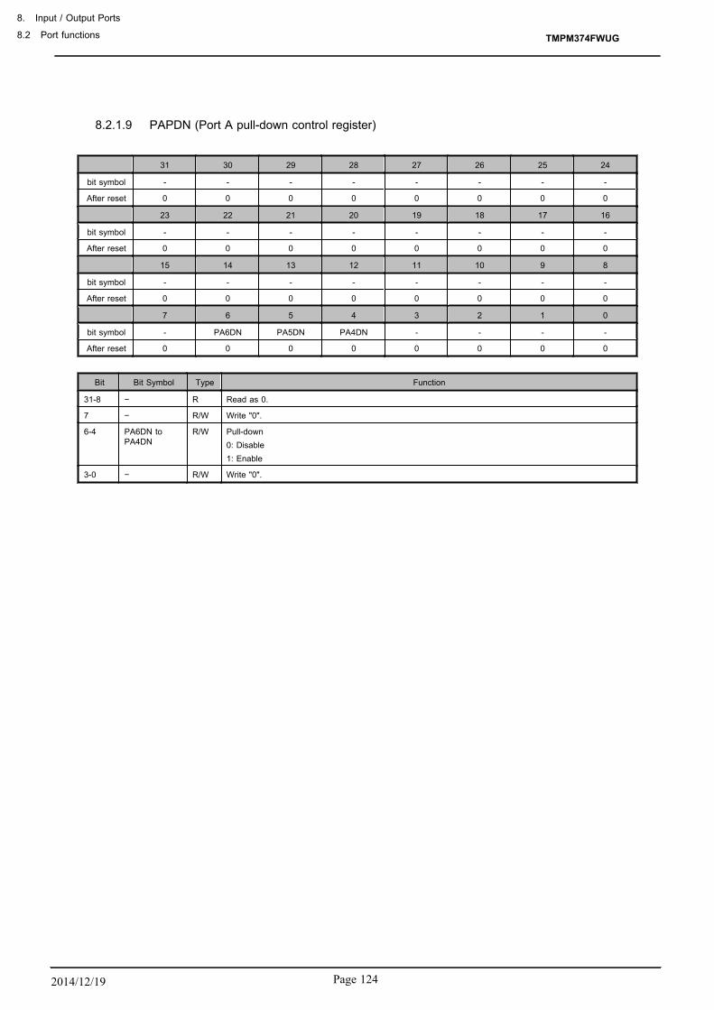
8.2.1.9 PAPDN (Port A pull-down control register)
31 30 29 28 27 26 25 24
bit symbol - - - - - - - -
After reset 0 0 0 0 0 0 0 0
23 22 21 20 19 18 17 16
bit symbol - - - - - - - -
After reset 0 0 0 0 0 0 0 0
15 14 13 12 11 10 9 8
bit symbol - - - - - - - -
After reset 0 0 0 0 0 0 0 0
7 6 5 4 3 2 1 0
bit symbol - PA6DN PA5DN PA4DN - - - -
After reset 0 0 0 0 0 0 0 0
Bit Bit Symbol Type Function
31-8 − R Read as 0.
7 − R/W Write "0".
6-4 PA6DN toPA4DN
R/W Pull-down0: Disable1: Enable
3-0 − R/W Write "0".
TMPM374FWUG
8. Input / Output Ports
8.2 Port functions
Page 1242014/12/19

8.2.1.10 PAIE (Port A input control register)
31 30 29 28 27 26 25 24
bit symbol - - - - - - - -
After reset 0 0 0 0 0 0 0 0
23 22 21 20 19 18 17 16
bit symbol - - - - - - - -
After reset 0 0 0 0 0 0 0 0
15 14 13 12 11 10 9 8
bit symbol - - - - - - - -
After reset 0 0 0 0 0 0 0 0
7 6 5 4 3 2 1 0
bit symbol - PA6IE PA5IE PA4IE - - - -
After reset 0 0 0 0 0 0 0 0
Bit Bit Symbol Type Function
31-8 − R Read as 0.
7 − R/W Write "0".
6-4 PA6IE to PA4IE R/W Input0: Disable1: Enable
3-0 − R/W Write "0".
TMPM374FWUG
Page 125 2014/12/19
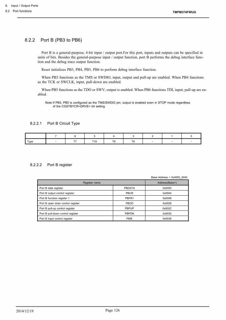
8.2.2 Port B (PB3 to PB6)
Port B is a general-purpose, 4-bit input / output port.For this port, inputs and outputs can be specified inunits of bits. Besides the general-purpose input / output function, port B performs the debug interface func-tion and the debug trace output function.
Reset initializes PB3, PB4, PB5, PB6 to perform debug interface function.
When PB3 functions as the TMS or SWDIO, input, output and pull-up are enabled. When PB4 functionsas the TCK or SWCLK, input, pull-down are enabled.
When PB5 functions as the TDO or SWV, output is enabled. When PB6 functions TDI, input, pull-up are en-abled.
Note:If PB3, PB5 is configured as the TMS/SWDIO pin, output is enabled even in STOP mode regardlessof the CGSTBYCR<DRVE> bit setting.
8.2.2.1 Port B Circuit Type
7 6 5 4 3 2 1 0
Type - T7 T19 T8 T6 - - -
8.2.2.2 Port B register
Base Address = 0x4000_0040
Register name Address(Base+)
Port B data register PBDATA 0x0000
Port B output control register PBCR 0x0004
Port B function register 1 PBFR1 0x0008
Port B open drain control register PBOD 0x0028
Port B pull-up control register PBPUP 0x002C
Port B pull-down control register PBPDN 0x0030
Port B input control register PBIE 0x0038
TMPM374FWUG
8. Input / Output Ports
8.2 Port functions
Page 1262014/12/19

8.2.2.3 PBDATA (Port B data register)
31 30 29 28 27 26 25 24
bit symbol - - - - - - - -
After reset 0 0 0 0 0 0 0 0
23 22 21 20 19 18 17 16
bit symbol - - - - - - - -
After reset 0 0 0 0 0 0 0 0
15 14 13 12 11 10 9 8
bit symbol - - - - - - - -
After reset 0 0 0 0 0 0 0 0
7 6 5 4 3 2 1 0
bit symbol - PB6 PB5 PB4 PB3 - - -
After reset 0 0 0 0 0 0 0 0
Bit Bit Symbol Type Function
31-8 − R Read as 0.
7 − R/W Write "0".
6-3 PB6 to PB3 R/W Port B data register
2-0 − R/W Write "0".
8.2.2.4 PBCR (Port B output control register)
31 30 29 28 27 26 25 24
bit symbol - - - - - - - -
After reset 0 0 0 0 0 0 0 0
23 22 21 20 19 18 17 16
bit symbol - - - - - - - -
After reset 0 0 0 0 0 0 0 0
15 14 13 12 11 10 9 8
bit symbol - - - - - - - -
After reset 0 0 0 0 0 0 0 0
7 6 5 4 3 2 1 0
bit symbol - PB6C PB5C PB4C PB3C - - -
After reset 0 0 1 0 1 0 0 0
Bit Bit Symbol Type Function
31-8 − R Read as 0.
7 − R/W Write "0".
6-3 PB6C to PB3C R/W Output0: Disable1: Enable
2-0 − R/W Write "0".
TMPM374FWUG
Page 127 2014/12/19

8.2.2.5 PBFR1 (Port B function register 1)
31 30 29 28 27 26 25 24
bit symbol - - - - - - - -
After reset 0 0 0 0 0 0 0 0
23 22 21 20 19 18 17 16
bit symbol - - - - - - - -
After reset 0 0 0 0 0 0 0 0
15 14 13 12 11 10 9 8
bit symbol - - - - - - - -
After reset 0 0 0 0 0 0 0 0
7 6 5 4 3 2 1 0
bit symbol - PB6F1 PB5F1 PB4F1 PB3F1 - - -
After reset 1 1 1 1 1 0 0 0
Bit Bit Symbol Type Function
31-8 − R Read as 0.
7 − R/W Write "0".
6 PB6F1 R/W 0: PORT1: TDI
5 PB5F1 R/W 0: PORT1: TDO / SWV
4 PB4F1 R/W 0: PORT1: TCK / SWCLK
3 PB3F1 R/W 0: PORT1: TMS / SWDIO
2-0 − R/W Write "0".
TMPM374FWUG
8. Input / Output Ports
8.2 Port functions
Page 1282014/12/19

8.2.2.6 PBOD (Port B open drain control register)
31 30 29 28 27 26 25 24
bit symbol - - - - - - - -
After reset 0 0 0 0 0 0 0 0
23 22 21 20 19 18 17 16
bit symbol - - - - - - - -
After reset 0 0 0 0 0 0 0 0
15 14 13 12 11 10 9 8
bit symbol - - - - - - - -
After reset 0 0 0 0 0 0 0 0
7 6 5 4 3 2 1 0
bit symbol - PB6OD PB5OD PB4OD PB3OD - - -
After reset 0 0 0 0 0 0 0 0
Bit Bit Symbol Type Function
31-8 − R Read as 0.
7 − R/W Write "0".
6-3 PB6OD toPB3OD
R/W 0 : CMOS1 : Open-drain
2-0 − R/W Write "0".
8.2.2.7 PBPUP (Port B pull-up control register)
31 30 29 28 27 26 25 24
bit symbol - - - - - - - -
After reset 0 0 0 0 0 0 0 0
23 22 21 20 19 18 17 16
bit symbol - - - - - - - -
After reset 0 0 0 0 0 0 0 0
15 14 13 12 11 10 9 8
bit symbol - - - - - - - -
After reset 0 0 0 0 0 0 0 0
7 6 5 4 3 2 1 0
bit symbol - PB6UP PB5UP PB4UP PB3UP - - -
After reset 1 1 0 0 1 0 0 0
Bit Bit Symbol Type Function
31-8 − R Read as 0.
7 − R/W Write "0".
6-3 PB6UP toPB3UP
R/W Pull-up0: Disable1: Enable
2-0 − R/W Write "0".
TMPM374FWUG
Page 129 2014/12/19
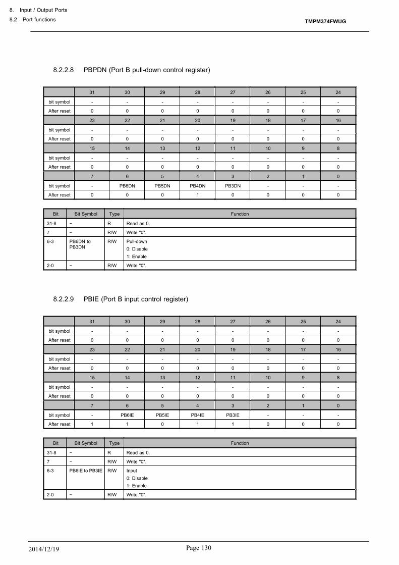
8.2.2.8 PBPDN (Port B pull-down control register)
31 30 29 28 27 26 25 24
bit symbol - - - - - - - -
After reset 0 0 0 0 0 0 0 0
23 22 21 20 19 18 17 16
bit symbol - - - - - - - -
After reset 0 0 0 0 0 0 0 0
15 14 13 12 11 10 9 8
bit symbol - - - - - - - -
After reset 0 0 0 0 0 0 0 0
7 6 5 4 3 2 1 0
bit symbol - PB6DN PB5DN PB4DN PB3DN - - -
After reset 0 0 0 1 0 0 0 0
Bit Bit Symbol Type Function
31-8 − R Read as 0.
7 − R/W Write "0".
6-3 PB6DN toPB3DN
R/W Pull-down0: Disable1: Enable
2-0 − R/W Write "0".
8.2.2.9 PBIE (Port B input control register)
31 30 29 28 27 26 25 24
bit symbol - - - - - - - -
After reset 0 0 0 0 0 0 0 0
23 22 21 20 19 18 17 16
bit symbol - - - - - - - -
After reset 0 0 0 0 0 0 0 0
15 14 13 12 11 10 9 8
bit symbol - - - - - - - -
After reset 0 0 0 0 0 0 0 0
7 6 5 4 3 2 1 0
bit symbol - PB6IE PB5IE PB4IE PB3IE - - -
After reset 1 1 0 1 1 0 0 0
Bit Bit Symbol Type Function
31-8 − R Read as 0.
7 − R/W Write "0".
6-3 PB6IE to PB3IE R/W Input0: Disable1: Enable
2-0 − R/W Write "0".
TMPM374FWUG
8. Input / Output Ports
8.2 Port functions
Page 1302014/12/19

8.2.3 Port E (PE0 to PE2,PE4,PE6 to 7)
Port E is a general-purpose, 6-bit input / output port. For this port, inputs and outputs can be specified inunits of bits. Besides the general-purpose input / output function, port E performs the serial interface func-tion (SIO / UART), the external signal interrupt input and the 16-bit timer input/output function.
The function registers are general-purpose ports after reset. Inputs or outputs with pull-up/-down are disabled.
Port E has two types of function register. If port E is used as a general-purpose port, set "0" to the correspond-ing bit of the two registers. If port E is used as other than a general-purpose port, set "1" to the correspond-ing bit of the function register.Do not set "1" to the some function registers at the same time.
To use the external interrupt input for releasing STOP mode, select this function in the PEFR2 and enable in-put in the PEIE register. These settings enable the interrupt input even if the CGSTBYCR<DRVE> bit in theclock / mode control block is set to stop driving of pins during STOP mode.
Note:In modes other than STOP mode, interrupt input is enabled regardless of the PxFR register setting ifinput is enabled in PxIE. Make sure to disable unused interrupts when programming the device.
8.2.3.1 Port E Circuit Type
7 6 5 4 3 2 1 0
Type T14 T12 - T12 - T9 T3 T2
8.2.3.2 Port E register
Base Address = 0x4000_0100
Register name Address(Base+)
Port E data register PEDATA 0x0000
Port E output control register PECR 0x0004
Port E function register 1 PEFR1 0x0008
Port E function register 2 PEFR2 0x000C
Port E open drain control register PEOD 0x0028
Port E pull-up control register PEPUP 0x002C
Port E pull-down control register PEPDN 0x0030
Port E input control register PEIE 0x0038
TMPM374FWUG
Page 131 2014/12/19

8.2.3.3 PEDATA (Port E data register)
31 30 29 28 27 26 25 24
bit symbol - - - - - - - -
After reset 0 0 0 0 0 0 0 0
23 22 21 20 19 18 17 16
bit symbol - - - - - - - -
After reset 0 0 0 0 0 0 0 0
15 14 13 12 11 10 9 8
bit symbol - - - - - - - -
After reset 0 0 0 0 0 0 0 0
7 6 5 4 3 2 1 0
bit symbol PE7 PE6 - PE4 - PE2 PE1 PE0
After reset 0 0 0 0 0 0 0 0
Bit Bit Symbol Type Function
31-8 − R Read as 0.
7-6 PE7 to PE6 R/W Port E data register
5 − R/W Write "0".
4 PE4 R/W Port E data register
3 − R/W Write "0".
2-0 PE2 to PE0 R/W Port E data register
TMPM374FWUG
8. Input / Output Ports
8.2 Port functions
Page 1322014/12/19

8.2.3.4 PECR (Port E output control register)
31 30 29 28 27 26 25 24
bit symbol - - - - - - - -
After reset 0 0 0 0 0 0 0 0
23 22 21 20 19 18 17 16
bit symbol - - - - - - - -
After reset 0 0 0 0 0 0 0 0
15 14 13 12 11 10 9 8
bit symbol - - - - - - - -
After reset 0 0 0 0 0 0 0 0
7 6 5 4 3 2 1 0
bit symbol PE7C PE6C - PE4C - PE2C PE1C PE0C
After reset 0 0 0 0 0 0 0 0
Bit Bit Symbol Type Function
31-8 − R Read as 0.
7-6 PE7C to PE6C R/W Output0: Disable1: Enable
5 − R/W Write "0".
4 PE4C R/W Output0: Disable1: Enable
3 − R/W Write "0".
2-0 PE2C to PE0C R/W Output0: Disable1: Enable
TMPM374FWUG
Page 133 2014/12/19

8.2.3.5 PEFR1 (Port E function register 1)
31 30 29 28 27 26 25 24
bit symbol - - - - - - - -
After reset 0 0 0 0 0 0 0 0
23 22 21 20 19 18 17 16
bit symbol - - - - - - - -
After reset 0 0 0 0 0 0 0 0
15 14 13 12 11 10 9 8
bit symbol - - - - - - - -
After reset 0 0 0 0 0 0 0 0
7 6 5 4 3 2 1 0
bit symbol PE7F1 PE6F1 - PE4F1 - PE2F1 PE1F1 PE0F1
After reset 0 0 0 0 0 0 0 0
Bit Bit Symbol Type Function
31-8 − R Read as 0.
7 PE7F1 R/W 0: PORT1:TB3OUT
6 PE6F1 R/W 0: PORT1:TB3IN
5 − R/W Write "0".
4 PE4F1 R/W 0: PORT1: TB2IN
3 − R/W Write "0".
2 PE2F1 R/W 0: PORT1: SCLK0
1 PE1F1 R/W 0: PORT1: RXD0
0 PE0F1 R/W 0: PORT1: TXD0
TMPM374FWUG
8. Input / Output Ports
8.2 Port functions
Page 1342014/12/19
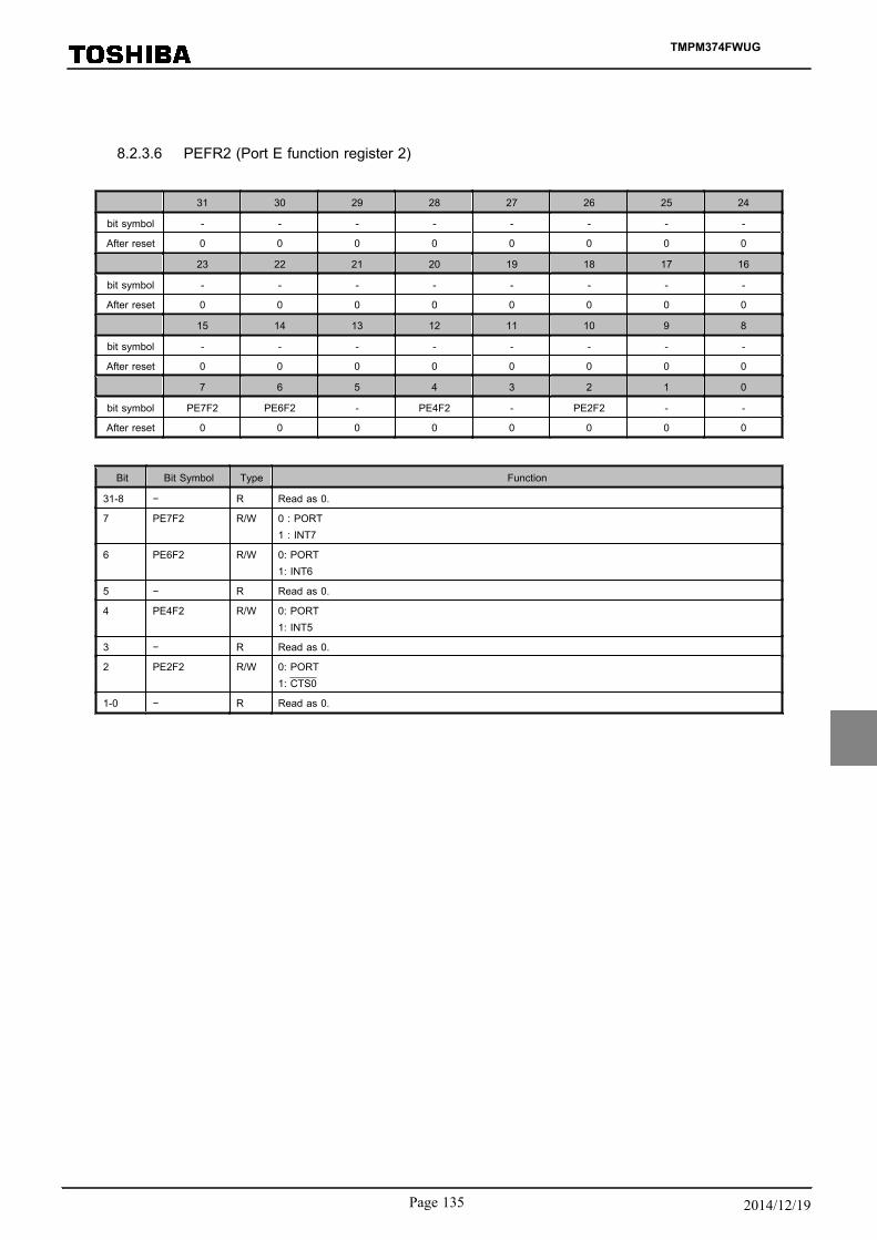
8.2.3.6 PEFR2 (Port E function register 2)
31 30 29 28 27 26 25 24
bit symbol - - - - - - - -
After reset 0 0 0 0 0 0 0 0
23 22 21 20 19 18 17 16
bit symbol - - - - - - - -
After reset 0 0 0 0 0 0 0 0
15 14 13 12 11 10 9 8
bit symbol - - - - - - - -
After reset 0 0 0 0 0 0 0 0
7 6 5 4 3 2 1 0
bit symbol PE7F2 PE6F2 - PE4F2 - PE2F2 - -
After reset 0 0 0 0 0 0 0 0
Bit Bit Symbol Type Function
31-8 − R Read as 0.
7 PE7F2 R/W 0 : PORT1 : INT7
6 PE6F2 R/W 0: PORT1: INT6
5 − R Read as 0.
4 PE4F2 R/W 0: PORT1: INT5
3 − R Read as 0.
2 PE2F2 R/W 0: PORT1: CTS0
1-0 − R Read as 0.
TMPM374FWUG
Page 135 2014/12/19

8.2.3.7 PEOD (Port E open drain control register)
31 30 29 28 27 26 25 24
bit symbol - - - - - - - -
After reset 0 0 0 0 0 0 0 0
23 22 21 20 19 18 17 16
bit symbol - - - - - - - -
After reset 0 0 0 0 0 0 0 0
15 14 13 12 11 10 9 8
bit symbol - - - - - - - -
After reset 0 0 0 0 0 0 0 0
7 6 5 4 3 2 1 0
bit symbol PE7OD PE6OD - PE4OD - PE2OD PE1OD PE0OD
After reset 0 0 0 0 0 0 0 0
Bit Bit Symbol Type Function
31-8 − R Read as 0.
7-6 PE7OD toPE6OD
R/W 0 : CMOS1 : Open-drain
5 − R/W Write "0".
4 PE4OD R/W 0 : CMOS1 : Open-drain
3 − R/W Write "0".
2-0 PE2OD toPE0OD
R/W 0 : CMOS1 : Open-drain
TMPM374FWUG
8. Input / Output Ports
8.2 Port functions
Page 1362014/12/19

8.2.3.8 PEPUP (Port E pull-up control register)
31 30 29 28 27 26 25 24
bit symbol - - - - - - - -
After reset 0 0 0 0 0 0 0 0
23 22 21 20 19 18 17 16
bit symbol - - - - - - - -
After reset 0 0 0 0 0 0 0 0
15 14 13 12 11 10 9 8
bit symbol - - - - - - - -
After reset 0 0 0 0 0 0 0 0
7 6 5 4 3 2 1 0
bit symbol PE7UP PE6UP - PE4UP - PE2UP PE1UP PE0UP
After reset 0 0 0 0 0 0 0 0
Bit Bit Symbol Type Function
31-8 − R Read as 0.
7-6 PE7UP toPE6UP
R/W Pull-up0: Disable1: Enable
5 − R/W Write "0".
4 PE4UP R/W Pull-up0: Disable1: Enable
3 − R/W Write "0".
2-0 PE2UP toPE0UP
R/W Pull-up0: Disable1: Enable
TMPM374FWUG
Page 137 2014/12/19
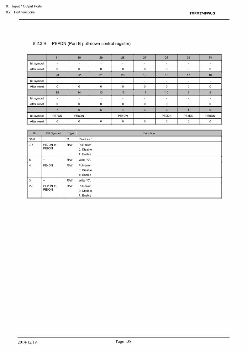
8.2.3.9 PEPDN (Port E pull-down control register)
31 30 29 28 27 26 25 24
bit symbol - - - - - - - -
After reset 0 0 0 0 0 0 0 0
23 22 21 20 19 18 17 16
bit symbol - - - - - - - -
After reset 0 0 0 0 0 0 0 0
15 14 13 12 11 10 9 8
bit symbol - - - - - - - -
After reset 0 0 0 0 0 0 0 0
7 6 5 4 3 2 1 0
bit symbol PE7DN PE6DN - PE4DN - PE2DN PE1DN PE0DN
After reset 0 0 0 0 0 0 0 0
Bit Bit Symbol Type Function
31-8 − R Read as 0.
7-6 PE7DN toPE6DN
R/W Pull-down0: Disable1: Enable
5 − R/W Write "0".
4 PE4DN R/W Pull-down0: Disable1: Enable
3 − R/W Write "0".
2-0 PE2DN toPE0DN
R/W Pull-down0: Disable1: Enable
TMPM374FWUG
8. Input / Output Ports
8.2 Port functions
Page 1382014/12/19

8.2.3.10 PEIE (Port E input control register)
31 30 29 28 27 26 25 24
bit symbol - - - - - - - -
After reset 0 0 0 0 0 0 0 0
23 22 21 20 19 18 17 16
bit symbol - - - - - - - -
After reset 0 0 0 0 0 0 0 0
15 14 13 12 11 10 9 8
bit symbol - - - - - - - -
After reset 0 0 0 0 0 0 0 0
7 6 5 4 3 2 1 0
bit symbol PE7IE PE6IE - PE4IE - PE2IE PE1IE PE0IE
After reset 0 0 0 0 0 0 0 0
Bit Bit Symbol Type Function
31-8 − R Read as 0.
7-6 PE7IE to PE6IE R/W Input0: Disable1: Enable
5 − R/W Write "0".
4 PE4IE R/W Input0: Disable1: Enable
3 − R/W Write "0".
2-0 PE2IE to PE0IE R/W Input0: Disable1: Enable
TMPM374FWUG
Page 139 2014/12/19

8.2.4 Port F (PF0, PF2 to PF4)
Port F is a general-purpose, 4-bit input / output port. For this port, inputs and outputs can be specified inunits of bits. Besides the general-purpose input / output function, port F performs the serial interface func-tion (SIO / UART), the 16-bit timer input/output function, the Encoder input function and the operationmode setting.
While a reset signal is in "0"state, the PF0 input and pull-up are enabled. At the rising edge of the reset sig-nal, if PF0 is "1", the device enters single mode and boots from the on-chip flash memory. If PF0 is "0", the de-vice enters single boot mode and boots from the internal boot program. For details of single boot mode, referto Chapter "Flash Memory Operation".
The function registers are general-purpose ports after reset. Inputs or outputs with pull-up/-down are disabled.
After a reset period ends, the PF0 pin input with pull-up is disabled according to the initial value of thePFIE register and the PFPUP register.
Pins other than the PF0 pin are general-purpose ports after reset. Inputs or outputs with pull-down are disa-bled.
8.2.4.1 Port F Circuit Type
7 6 5 4 3 2 1 0
Type − − − T11 T10 T15 - T20
8.2.4.2 Port F register
Base Address = 0x4000_0140
Register name Address(Base+)
Port F data register PFDATA 0x0000
Port F output control register PFCR 0x0004
Port F function register 1 PFFR1 0x0008
Port F function register 2 PFFR2 0x000C
Port F function register 3 PFFR3 0x0010
Port F open drain control register PFOD 0x0028
Port F pull-up control register PFPUP 0x002C
Port F pull-down control register PFPDN 0x0030
Port F input control register PFIE 0x0038
TMPM374FWUG
8. Input / Output Ports
8.2 Port functions
Page 1402014/12/19

8.2.4.3 PFDATA (Port F data register)
31 30 29 28 27 26 25 24
bit symbol - - - - - - - -
After reset 0 0 0 0 0 0 0 0
23 22 21 20 19 18 17 16
bit symbol - - - - - - - -
After reset 0 0 0 0 0 0 0 0
15 14 13 12 11 10 9 8
bit symbol - - - - - - - -
After reset 0 0 0 0 0 0 0 0
7 6 5 4 3 2 1 0
bit symbol - - - PF4 PF3 PF2 - PF0
After reset 0 0 0 0 0 0 0 0
Bit Bit Symbol Type Function
31-5 − R Read as 0.
4-2 PF4 to PF2 R/W Port F data register
1 − R/W Write "0".
0 PF0 R/W Port F data register
TMPM374FWUG
Page 141 2014/12/19
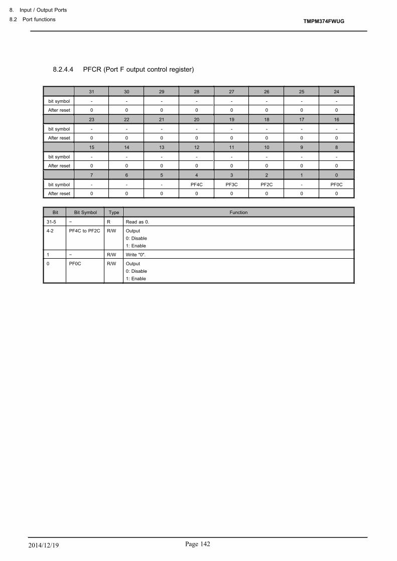
8.2.4.4 PFCR (Port F output control register)
31 30 29 28 27 26 25 24
bit symbol - - - - - - - -
After reset 0 0 0 0 0 0 0 0
23 22 21 20 19 18 17 16
bit symbol - - - - - - - -
After reset 0 0 0 0 0 0 0 0
15 14 13 12 11 10 9 8
bit symbol - - - - - - - -
After reset 0 0 0 0 0 0 0 0
7 6 5 4 3 2 1 0
bit symbol - - - PF4C PF3C PF2C - PF0C
After reset 0 0 0 0 0 0 0 0
Bit Bit Symbol Type Function
31-5 − R Read as 0.
4-2 PF4C to PF2C R/W Output0: Disable1: Enable
1 − R/W Write "0".
0 PF0C R/W Output0: Disable1: Enable
TMPM374FWUG
8. Input / Output Ports
8.2 Port functions
Page 1422014/12/19
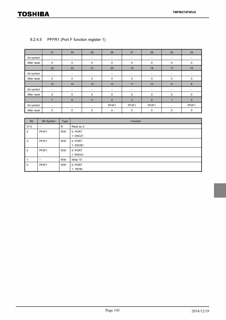
8.2.4.5 PFFR1 (Port F function register 1)
31 30 29 28 27 26 25 24
bit symbol - - - - - - - -
After reset 0 0 0 0 0 0 0 0
23 22 21 20 19 18 17 16
bit symbol - - - - - - - -
After reset 0 0 0 0 0 0 0 0
15 14 13 12 11 10 9 8
bit symbol - - - - - - - -
After reset 0 0 0 0 0 0 0 0
7 6 5 4 3 2 1 0
bit symbol - - - PF4F1 PF3F1 PF2F1 - PF0F1
After reset 0 0 0 0 0 0 0 0
Bit Bit Symbol Type Function
31-5 − R Read as 0.
4 PF4F1 R/W 0: PORT1: ENCZ1
3 PF3F1 R/W 0: PORT1: ENCB1
2 PF2F1 R/W 0: PORT1: ENCA1
1 − R/W Write "0".
0 PF0F1 R/W 0: PORT1: TB7IN
TMPM374FWUG
Page 143 2014/12/19

8.2.4.6 PFFR2 (Port F function register 2)
31 30 29 28 27 26 25 24
bit symbol - - - - - - - -
After reset 0 0 0 0 0 0 0 0
23 22 21 20 19 18 17 16
bit symbol - - - - - - - -
After reset 0 0 0 0 0 0 0 0
15 14 13 12 11 10 9 8
bit symbol - - - - - - - -
After reset 0 0 0 0 0 0 0 0
7 6 5 4 3 2 1 0
bit symbol - - - PF4F2 PF3F2 PF2F2 - -
After reset 0 0 0 0 0 0 0 0
Bit Bit Symbol Type Function
31-5 − R Read as 0.
4 PF4F2 R/W 0: PORT1: RXD3
3 PF3F2 R/W 0: PORT1: TXD3
2 PF2F2 R/W 0: PORT1: SCLK3
1-0 − R Read as 0.
8.2.4.7 PFFR3 (Port F function register 3)
31 30 29 28 27 26 25 24
bit symbol - - - - - - - -
After reset 0 0 0 0 0 0 0 0
23 22 21 20 19 18 17 16
bit symbol - - - - - - - -
After reset 0 0 0 0 0 0 0 0
15 14 13 12 11 10 9 8
bit symbol - - - - - - - -
After reset 0 0 0 0 0 0 0 0
7 6 5 4 3 2 1 0
bit symbol - - - - - PF2F3 - -
After reset 0 0 0 0 0 0 0 0
Bit Bit Symbol Type Function
31-3 − R Read as 0.
2 PF2F3 R/W 0: PORT1: CTS3
1-0 − R Read as 0.
TMPM374FWUG
8. Input / Output Ports
8.2 Port functions
Page 1442014/12/19

8.2.4.8 PFOD (Port F open drain control register)
31 30 29 28 27 26 25 24
bit symbol - - - - - - - -
After reset 0 0 0 0 0 0 0 0
23 22 21 20 19 18 17 16
bit symbol - - - - - - - -
After reset 0 0 0 0 0 0 0 0
15 14 13 12 11 10 9 8
bit symbol - - - - - - - -
After reset 0 0 0 0 0 0 0 0
7 6 5 4 3 2 1 0
bit symbol - - - PF4OD PF3OD PF2OD - PF0OD
After reset 0 0 0 0 0 0 0 0
Bit Bit Symbol Type Function
31-5 − R Read as 0.
4-2 PF4OD toPF2OD
R/W 0 : CMOS1 : Open-drain
1 − R/W Write "0".
0 PF0OD R/W 0 : CMOS1 : Open-drain
TMPM374FWUG
Page 145 2014/12/19

8.2.4.9 PFPUP (Port F pull-up control register)
31 30 29 28 27 26 25 24
bit symbol - - - - - - - -
After reset 0 0 0 0 0 0 0 0
23 22 21 20 19 18 17 16
bit symbol - - - - - - - -
After reset 0 0 0 0 0 0 0 0
15 14 13 12 11 10 9 8
bit symbol - - - - - - - -
After reset 0 0 0 0 0 0 0 0
7 6 5 4 3 2 1 0
bit symbol - - - PF4UP PF3UP PF2UP - PF0UP
After reset 0 0 0 0 0 0 0 0
Bit Bit Symbol Type Function
31-5 − R Read as 0.
4-2 PF4UP toPF2UP
R/W Pull-up0: Disable1: Enable
1 − R/W Write "0".
0 PF0UP R/W Pull-up0: Disable1: Enable
TMPM374FWUG
8. Input / Output Ports
8.2 Port functions
Page 1462014/12/19

8.2.4.10 PFPDN (Port F pull-down control register)
31 30 29 28 27 26 25 24
bit symbol - - - - - - - -
After reset 0 0 0 0 0 0 0 0
23 22 21 20 19 18 17 16
bit symbol - - - - - - - -
After reset 0 0 0 0 0 0 0 0
15 14 13 12 11 10 9 8
bit symbol - - - - - - - -
After reset 0 0 0 0 0 0 0 0
7 6 5 4 3 2 1 0
bit symbol - - - PF4DN PF3DN PF2DN - PF0DN
After reset 0 0 0 0 0 0 0 0
Bit Bit Symbol Type Function
31-5 − R Read as 0.
4-2 PF4DN toPF2DN
R/W Pull-down0: Disable1: Enable
1 − R/W Write "0".
0 PF0DN R/W Pull-down0: Disable1: Enable
TMPM374FWUG
Page 147 2014/12/19

8.2.4.11 PFIE (Port F input control register)
31 30 29 28 27 26 25 24
bit symbol - - - - - - - -
After reset 0 0 0 0 0 0 0 0
23 22 21 20 19 18 17 16
bit symbol - - - - - - - -
After reset 0 0 0 0 0 0 0 0
15 14 13 12 11 10 9 8
bit symbol - - - - - - - -
After reset 0 0 0 0 0 0 0 0
7 6 5 4 3 2 1 0
bit symbol - - - PF4IE PF3IE PF2IE - PF0IE
After reset 0 0 0 0 0 0 0 0
Bit Bit Symbol Type Function
31-5 − R Read as 0.
4-2 PF4IE to PF2IE R/W Input0: Disable1: Enable
1 − R/W Write "0".
0 PF0IE R/W Input0: Disable1: Enable
TMPM374FWUG
8. Input / Output Ports
8.2 Port functions
Page 1482014/12/19
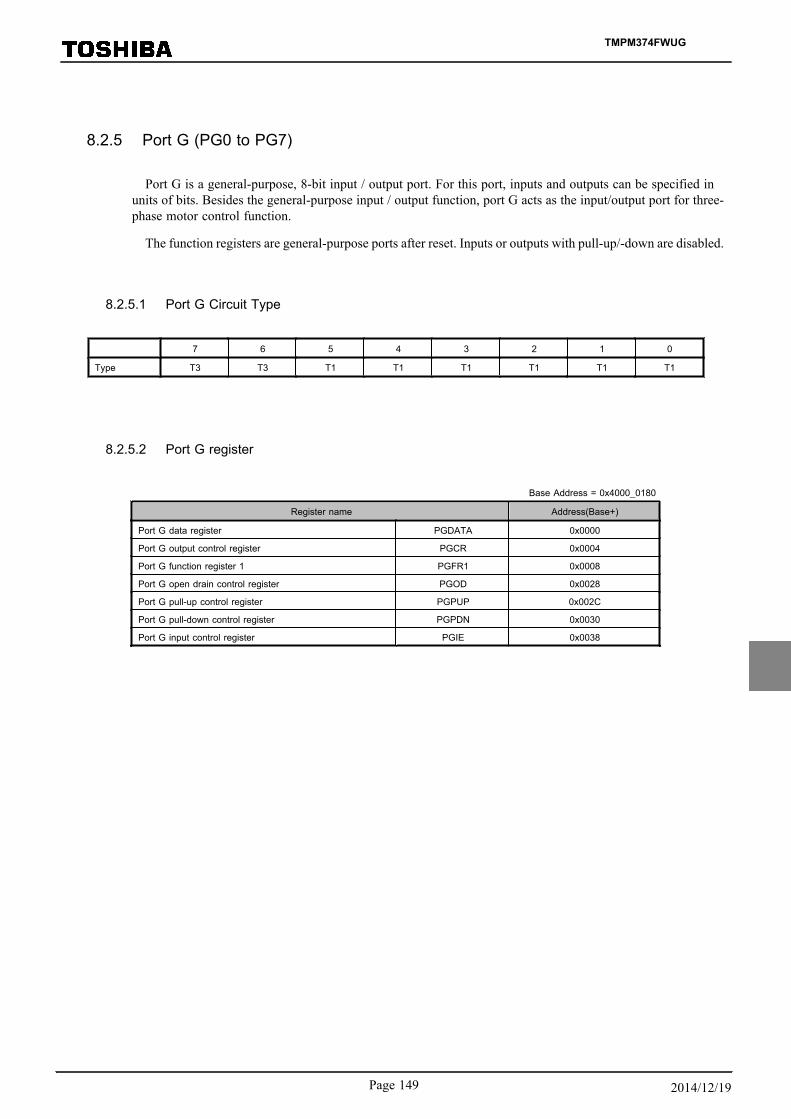
8.2.5 Port G (PG0 to PG7)
Port G is a general-purpose, 8-bit input / output port. For this port, inputs and outputs can be specified inunits of bits. Besides the general-purpose input / output function, port G acts as the input/output port for three-phase motor control function.
The function registers are general-purpose ports after reset. Inputs or outputs with pull-up/-down are disabled.
8.2.5.1 Port G Circuit Type
7 6 5 4 3 2 1 0
Type T3 T3 T1 T1 T1 T1 T1 T1
8.2.5.2 Port G register
Base Address = 0x4000_0180
Register name Address(Base+)
Port G data register PGDATA 0x0000
Port G output control register PGCR 0x0004
Port G function register 1 PGFR1 0x0008
Port G open drain control register PGOD 0x0028
Port G pull-up control register PGPUP 0x002C
Port G pull-down control register PGPDN 0x0030
Port G input control register PGIE 0x0038
TMPM374FWUG
Page 149 2014/12/19

8.2.5.3 PGDATA (Port G data register)
31 30 29 28 27 26 25 24
bit symbol - - - - - - - -
After reset 0 0 0 0 0 0 0 0
23 22 21 20 19 18 17 16
bit symbol - - - - - - - -
After reset 0 0 0 0 0 0 0 0
15 14 13 12 11 10 9 8
bit symbol - - - - - - - -
After reset 0 0 0 0 0 0 0 0
7 6 5 4 3 2 1 0
bit symbol PG7 PG6 PG5 PG4 PG3 PG2 PG1 PG0
After reset 0 0 0 0 0 0 0 0
Bit Bit Symbol Type Function
31-8 − R Read as 0.
7-0 PG7 to PG0 R/W Port G data register
8.2.5.4 PGCR (Port G output control register)
31 30 29 28 27 26 25 24
bit symbol - - - - - - - -
After reset 0 0 0 0 0 0 0 0
23 22 21 20 19 18 17 16
bit symbol - - - - - - - -
After reset 0 0 0 0 0 0 0 0
15 14 13 12 11 10 9 8
bit symbol - - - - - - - -
After reset 0 0 0 0 0 0 0 0
7 6 5 4 3 2 1 0
bit symbol PG7C PG6C PG5C PG4C PG3C PG2C PG1C PG0C
After reset 0 0 0 0 0 0 0 0
Bit Bit Symbol Type Function
31-8 − R Read as 0.
7-0 PG7C to PG0C R/W Output0: Disable1: Enable
TMPM374FWUG
8. Input / Output Ports
8.2 Port functions
Page 1502014/12/19

8.2.5.5 PGFR1 (Port G function register 1)
31 30 29 28 27 26 25 24
bit symbol - - - - - - - -
After reset 0 0 0 0 0 0 0 0
23 22 21 20 19 18 17 16
bit symbol - - - - - - - -
After reset 0 0 0 0 0 0 0 0
15 14 13 12 11 10 9 8
bit symbol - - - - - - - -
After reset 0 0 0 0 0 0 0 0
7 6 5 4 3 2 1 0
bit symbol PG7F1 PG6F1 PG5F1 PG4F1 PG3F1 PG2F1 PG1F1 PG0F1
After reset 0 0 0 0 0 0 0 0
Bit Bit Symbol Type Function
31-8 − R Read as 0.
7 PG7F1 R/W 0: PORT1:OVV1
6 PG6F1 R/W 0: PORT1: EMG1
5 PG5F1 R/W 0: PORT1: ZO1
4 PG4F1 R/W 0: PORT1: WO1
3 PG3F1 R/W 0: PORT1: YO1
2 PG2F1 R/W 0: PORT1: VO1
1 PG1F1 R/W 0: PORT1: XO1
0 PG0F1 R/W 0: PORT1: UO1
TMPM374FWUG
Page 151 2014/12/19

8.2.5.6 PGOD (Port G open drain control register)
31 30 29 28 27 26 25 24
bit symbol - - - - - - - -
After reset 0 0 0 0 0 0 0 0
23 22 21 20 19 18 17 16
bit symbol - - - - - - - -
After reset 0 0 0 0 0 0 0 0
15 14 13 12 11 10 9 8
bit symbol - - - - - - - -
After reset 0 0 0 0 0 0 0 0
7 6 5 4 3 2 1 0
bit symbol PG7OD PG6OD PG5OD PG4OD PG3OD PG2OD PG1OD PG0OD
After reset 0 0 0 0 0 0 0 0
Bit Bit Symbol Type Function
31-8 − R Read as 0.
7-0 PG7OD toPG0OD
R/W 0 : CMOS1 : Open-drain
8.2.5.7 PGPUP (Port G pull-up control register)
31 30 29 28 27 26 25 24
bit symbol - - - - - - - -
After reset 0 0 0 0 0 0 0 0
23 22 21 20 19 18 17 16
bit symbol - - - - - - - -
After reset 0 0 0 0 0 0 0 0
15 14 13 12 11 10 9 8
bit symbol - - - - - - - -
After reset 0 0 0 0 0 0 0 0
7 6 5 4 3 2 1 0
bit symbol PG7UP PG6UP PG5UP PG4UP PG3UP PG2UP PG1UP PG0UP
After reset 0 0 0 0 0 0 0 0
Bit Bit Symbol Type Function
31-8 − R Read as 0.
7-0 PG7UP toPG0UP
R/W Pull-up0: Disable1: Enable
TMPM374FWUG
8. Input / Output Ports
8.2 Port functions
Page 1522014/12/19

8.2.5.8 PGPDN (Port G pull-down control register)
31 30 29 28 27 26 25 24
bit symbol - - - - - - - -
After reset 0 0 0 0 0 0 0 0
23 22 21 20 19 18 17 16
bit symbol - - - - - - - -
After reset 0 0 0 0 0 0 0 0
15 14 13 12 11 10 9 8
bit symbol - - - - - - - -
After reset 0 0 0 0 0 0 0 0
7 6 5 4 3 2 1 0
bit symbol PG7DN PG6DN PG5DN PG4DN PG3DN PG2DN PG1DN PG0DN
After reset 0 0 0 0 0 0 0 0
Bit Bit Symbol Type Function
31-8 − R Read as 0.
7-0 PG7DN toPG0DN
R/W Pull-down0: Disable1: Enable
8.2.5.9 PGIE (Port G input control register)
31 30 29 28 27 26 25 24
bit symbol - - - - - - - -
After reset 0 0 0 0 0 0 0 0
23 22 21 20 19 18 17 16
bit symbol - - - - - - - -
After reset 0 0 0 0 0 0 0 0
15 14 13 12 11 10 9 8
bit symbol - - - - - - - -
After reset 0 0 0 0 0 0 0 0
7 6 5 4 3 2 1 0
bit symbol PG7IE PG6IE PG5IE PG4IE PG3IE PG2IE PG1IE PG0IE
After reset 0 0 0 0 0 0 0 0
Bit Bit Symbol Type Function
31-8 − R Read as 0.
7-0 PG7IE toPG0IE
R/W Input0: Disable1: Enable
TMPM374FWUG
Page 153 2014/12/19

8.2.6 Port I (PI3)
Port I is a general-purpose, 1-bit input / output port. For this port, inputs and outputs can be specified inunits of bits. Besides the general-purpose input / output function, port I performs the analog input of the AD con-verter.
The function registers are general-purpose ports after reset. Inputs or outputs with pull-up/-down are disabled.
Note:Unless all the bits of port I are used as analog input pins, conversion accuracy may be reduced. Besure to verify that this causes no problem on your system.
8.2.6.1 Port I Circuit Type
7 6 5 4 3 2 1 0
Type − − − − T16 - - -
8.2.6.2 Port I register
Base Address = 0x4000_0200
Register name Address(Base+)
Port I data register PIDATA 0x0000
Port I output control register PICR 0x0004
Port I open drain control register PIOD 0x0028
Port I pull-up control register PIPUP 0x002C
Port I pull-down control register PIPDN 0x0030
Port I input control register PIIE 0x0038
TMPM374FWUG
8. Input / Output Ports
8.2 Port functions
Page 1542014/12/19

8.2.6.3 PIDATA (Port I data register)
31 30 29 28 27 26 25 24
bit symbol - - - - - - - -
After reset 0 0 0 0 0 0 0 0
23 22 21 20 19 18 17 16
bit symbol - - - - - - - -
After reset 0 0 0 0 0 0 0 0
15 14 13 12 11 10 9 8
bit symbol - - - - - - - -
After reset 0 0 0 0 0 0 0 0
7 6 5 4 3 2 1 0
bit symbol - - - - PI3 - - -
After reset 0 0 0 0 0 0 0 0
Bit Bit Symbol Type Function
31-4 − R Read as 0.
3 PI3 R/W Port I data register
2-0 − R/W Read as 0.
8.2.6.4 PICR (Port I output control register)
31 30 29 28 27 26 25 24
bit symbol - - - - - - - -
After reset 0 0 0 0 0 0 0 0
23 22 21 20 19 18 17 16
bit symbol - - - - - - - -
After reset 0 0 0 0 0 0 0 0
15 14 13 12 11 10 9 8
bit symbol - - - - - - - -
After reset 0 0 0 0 0 0 0 0
7 6 5 4 3 2 1 0
bit symbol - - - - PI3C - - -
After reset 0 0 0 0 0 0 0 0
Bit Bit Symbol Type Function
31-4 − R Read as 0.
3 PI3C R/W Output0: Disable1: Enable
2-0 − R/W Read as 0.
TMPM374FWUG
Page 155 2014/12/19

8.2.6.5 PIOD (Port I open drain control register)
31 30 29 28 27 26 25 24
bit symbol - - - - - - - -
After reset 0 0 0 0 0 0 0 0
23 22 21 20 19 18 17 16
bit symbol - - - - - - - -
After reset 0 0 0 0 0 0 0 0
15 14 13 12 11 10 9 8
bit symbol - - - - - - - -
After reset 0 0 0 0 0 0 0 0
7 6 5 4 3 2 1 0
bit symbol - - - - PI3OD - - -
After reset 0 0 0 0 0 0 0 0
Bit Bit Symbol Type Function
31-4 − R Read as 0.
3 PI3OD R/W 0 : CMOS1 : Open-drain
2-0 − R/W Read as 0.
8.2.6.6 PIPUP (Port I pull-up control register)
31 30 29 28 27 26 25 24
bit symbol - - - - - - - -
After reset 0 0 0 0 0 0 0 0
23 22 21 20 19 18 17 16
bit symbol - - - - - - - -
After reset 0 0 0 0 0 0 0 0
15 14 13 12 11 10 9 8
bit symbol - - - - - - - -
After reset 0 0 0 0 0 0 0 0
7 6 5 4 3 2 1 0
bit symbol - - - - PI3UP - - -
After reset 0 0 0 0 0 0 0 0
Bit Bit Symbol Type Function
31-4 − R Read as 0.
3 PI3UP R/W Pull-up0: Disable1: Enable
2-0 − R/W Read as 0.
TMPM374FWUG
8. Input / Output Ports
8.2 Port functions
Page 1562014/12/19
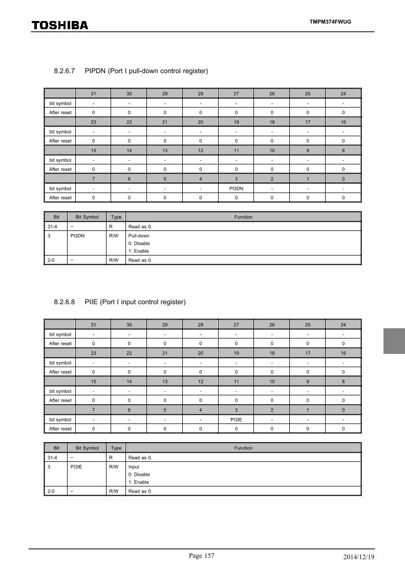
8.2.6.7 PIPDN (Port I pull-down control register)
31 30 29 28 27 26 25 24
bit symbol - - - - - - - -
After reset 0 0 0 0 0 0 0 0
23 22 21 20 19 18 17 16
bit symbol - - - - - - - -
After reset 0 0 0 0 0 0 0 0
15 14 13 12 11 10 9 8
bit symbol - - - - - - - -
After reset 0 0 0 0 0 0 0 0
7 6 5 4 3 2 1 0
bit symbol - - - - PI3DN - - -
After reset 0 0 0 0 0 0 0 0
Bit Bit Symbol Type Function
31-4 − R Read as 0.
3 PI3DN R/W Pull-down0: Disable1: Enable
2-0 − R/W Read as 0.
8.2.6.8 PIIE (Port I input control register)
31 30 29 28 27 26 25 24
bit symbol - - - - - - - -
After reset 0 0 0 0 0 0 0 0
23 22 21 20 19 18 17 16
bit symbol - - - - - - - -
After reset 0 0 0 0 0 0 0 0
15 14 13 12 11 10 9 8
bit symbol - - - - - - - -
After reset 0 0 0 0 0 0 0 0
7 6 5 4 3 2 1 0
bit symbol - - - - PI3IE - - -
After reset 0 0 0 0 0 0 0 0
Bit Bit Symbol Type Function
31-4 − R Read as 0.
3 PI3IE R/W Input0: Disable1: Enable
2-0 − R/W Read as 0.
TMPM374FWUG
Page 157 2014/12/19

8.2.7 Port J (PJ0,PJ6 to PJ7)
Port J is a general-purpose, 3-bit input / output port. For this port, inputs and outputs can be specified inunits of bits. Besides the general-purpose input / output function, port J performs the analog input of the AD con-verter and the external signal interrupt input.
The function registers are general-purpose ports after reset. Inputs or outputs with pull-up/-down are disabled.
To use the external interrupt input for releasing STOP mode, select this function in the PJFR1 and enable in-put in the PJIE register. These settings enable the interrupt input even if the CGSTBYCR<DRVE> bit in theclock / mode control block is set to stop driving of pins during STOP mode.
Note 1: Unless all the bits of port J are used as analog input pins, conversion accuracy may be reduced. Besure to verify that this causes no problem on your system.
Note 2: In modes other than STOP mode, interrupt input is enabled regardless of the PxFR register setting if in-put is enabled in PxIE. Make sure to disable unused interrupts when programming the device.
8.2.7.1 Port J Circuit Type
7 6 5 4 3 2 1 0
Type T17 T17 - - - - - T16
8.2.7.2 Port J register
Base Address = 0x4000_0240
Register name Address(Base+)
Port J data register PJDATA 0x0000
Port J output control register PJCR 0x0004
Port J function register 1 PJFR1 0x0008
Port J open drain control register PJOD 0x0028
Port J pull-up control register PJPUP 0x002C
Port J pull-down control register PJPDN 0x0030
Port J input control register PJIE 0x0038
TMPM374FWUG
8. Input / Output Ports
8.2 Port functions
Page 1582014/12/19

8.2.7.3 PJDATA (Port J data register)
31 30 29 28 27 26 25 24
bit symbol - - - - - - - -
After reset 0 0 0 0 0 0 0 0
23 22 21 20 19 18 17 16
bit symbol - - - - - - - -
After reset 0 0 0 0 0 0 0 0
15 14 13 12 11 10 9 8
bit symbol - - - - - - - -
After reset 0 0 0 0 0 0 0 0
7 6 5 4 3 2 1 0
bit symbol PJ7 PJ6 - - - - - PJ0
After reset 0 0 0 0 0 0 0 0
Bit Bit Symbol Type Function
31-8 − R Read as 0.
7-6 PJ7 to PJ6 R/W Port J data register
5-1 − R/W Write "0".
0 PJ0 R/W Port J data register
TMPM374FWUG
Page 159 2014/12/19

8.2.7.4 PJCR (Port J output control register)
31 30 29 28 27 26 25 24
bit symbol - - - - - - - -
After reset 0 0 0 0 0 0 0 0
23 22 21 20 19 18 17 16
bit symbol - - - - - - - -
After reset 0 0 0 0 0 0 0 0
15 14 13 12 11 10 9 8
bit symbol - - - - - - - -
After reset 0 0 0 0 0 0 0 0
7 6 5 4 3 2 1 0
bit symbol PJ7C PJ6C - - - - - PJ0C
After reset 0 0 0 0 0 0 0 0
Bit Bit Symbol Type Function
31-8 − R Read as 0.
7-6 PJ7C to PJ6C R/W Output0: Disable1: Enable
5-1 − R/W Write "0".
0 PJ0C R/W Output0: Disable1: Enable
TMPM374FWUG
8. Input / Output Ports
8.2 Port functions
Page 1602014/12/19
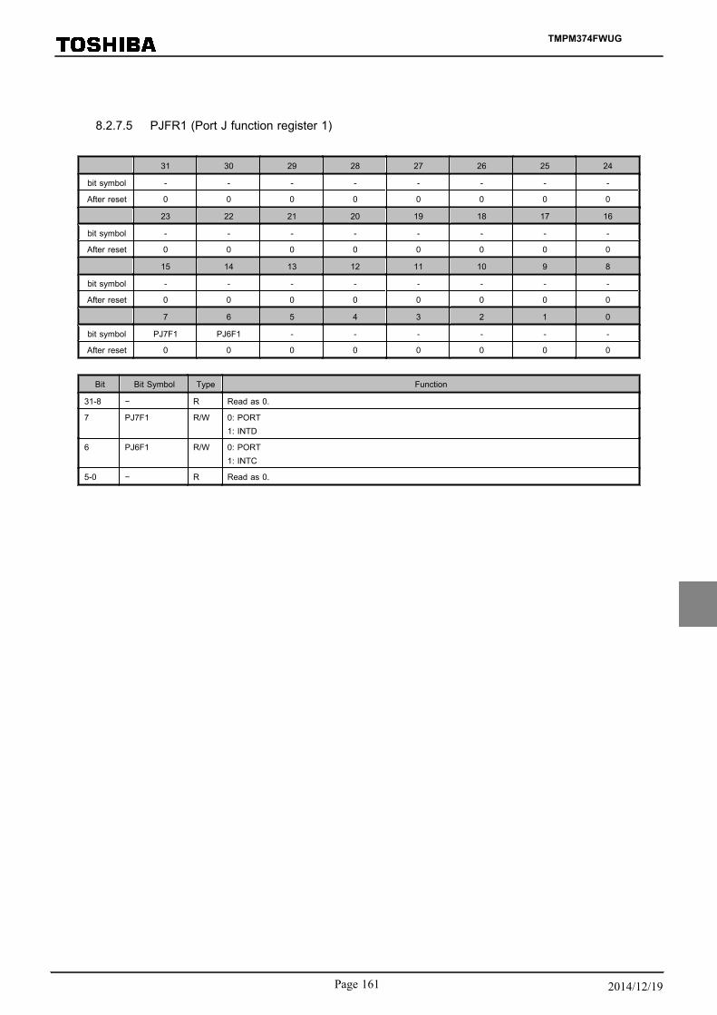
8.2.7.5 PJFR1 (Port J function register 1)
31 30 29 28 27 26 25 24
bit symbol - - - - - - - -
After reset 0 0 0 0 0 0 0 0
23 22 21 20 19 18 17 16
bit symbol - - - - - - - -
After reset 0 0 0 0 0 0 0 0
15 14 13 12 11 10 9 8
bit symbol - - - - - - - -
After reset 0 0 0 0 0 0 0 0
7 6 5 4 3 2 1 0
bit symbol PJ7F1 PJ6F1 - - - - - -
After reset 0 0 0 0 0 0 0 0
Bit Bit Symbol Type Function
31-8 − R Read as 0.
7 PJ7F1 R/W 0: PORT1: INTD
6 PJ6F1 R/W 0: PORT1: INTC
5-0 − R Read as 0.
TMPM374FWUG
Page 161 2014/12/19

8.2.7.6 PJOD (Port J open drain control register)
31 30 29 28 27 26 25 24
bit symbol - - - - - - - -
After reset 0 0 0 0 0 0 0 0
23 22 21 20 19 18 17 16
bit symbol - - - - - - - -
After reset 0 0 0 0 0 0 0 0
15 14 13 12 11 10 9 8
bit symbol - - - - - - - -
After reset 0 0 0 0 0 0 0 0
7 6 5 4 3 2 1 0
bit symbol PJ7OD PJ6OD - - - - - PJ0OD
After reset 0 0 0 0 0 0 0 0
Bit Bit Symbol Type Function
31-8 − R Read as 0.
7-6 PJ7OD toPJ6OD
R/W 0 : CMOS1 : Open-drain
5-1 − R/W Write "0".
0 PJ0OD R/W 0 : CMOS1 : Open-drain
TMPM374FWUG
8. Input / Output Ports
8.2 Port functions
Page 1622014/12/19

8.2.7.7 PJPUP (Port J pull-up control register)
31 30 29 28 27 26 25 24
bit symbol - - - - - - - -
After reset 0 0 0 0 0 0 0 0
23 22 21 20 19 18 17 16
bit symbol - - - - - - - -
After reset 0 0 0 0 0 0 0 0
15 14 13 12 11 10 9 8
bit symbol - - - - - - - -
After reset 0 0 0 0 0 0 0 0
7 6 5 4 3 2 1 0
bit symbol PJ7UP PJ6UP - - - - - PJ0UP
After reset 0 0 0 0 0 0 0 0
Bit Bit Symbol Type Function
31-8 − R Read as 0.
7-6 PJ7UP toPJ6UP
R/W Pull-up0: Disable1: Enable
5-1 − R/W Write "0".
0 PJ0UP R/W Pull-up0: Disable1: Enable
TMPM374FWUG
Page 163 2014/12/19

8.2.7.8 PJPDN (Port J pull-down control register)
31 30 29 28 27 26 25 24
bit symbol - - - - - - - -
After reset 0 0 0 0 0 0 0 0
23 22 21 20 19 18 17 16
bit symbol - - - - - - - -
After reset 0 0 0 0 0 0 0 0
15 14 13 12 11 10 9 8
bit symbol - - - - - - - -
After reset 0 0 0 0 0 0 0 0
7 6 5 4 3 2 1 0
bit symbol PJ7DN PJ6DN - - - - - PJ0DN
After reset 0 0 0 0 0 0 0 0
Bit Bit Symbol Type Function
31-8 − R Read as 0.
7-6 PJ7DN toPJ6DN
R/W Pull-down0: Disable1: Enable
5-1 − R/W Write "0".
0 PJ0DN R/W Pull-down0: Disable1: Enable
TMPM374FWUG
8. Input / Output Ports
8.2 Port functions
Page 1642014/12/19

8.2.7.9 PJIE (Port J input control register)
31 30 29 28 27 26 25 24
bit symbol - - - - - - - -
After reset 0 0 0 0 0 0 0 0
23 22 21 20 19 18 17 16
bit symbol - - - - - - - -
After reset 0 0 0 0 0 0 0 0
15 14 13 12 11 10 9 8
bit symbol - - - - - - - -
After reset 0 0 0 0 0 0 0 0
7 6 5 4 3 2 1 0
bit symbol PJ7IE PJ6IE - - - - - PJ0IE
After reset 0 0 0 0 0 0 0 0
Bit Bit Symbol Type Function
31-8 − R Read as 0.
7-6 PJ7IE to PJ6IE R/W Input0: Disable1: Enable
5-1 − R/W Write "0".
0 PJ0IE R/W Input0: Disable1: Enable
TMPM374FWUG
Page 165 2014/12/19
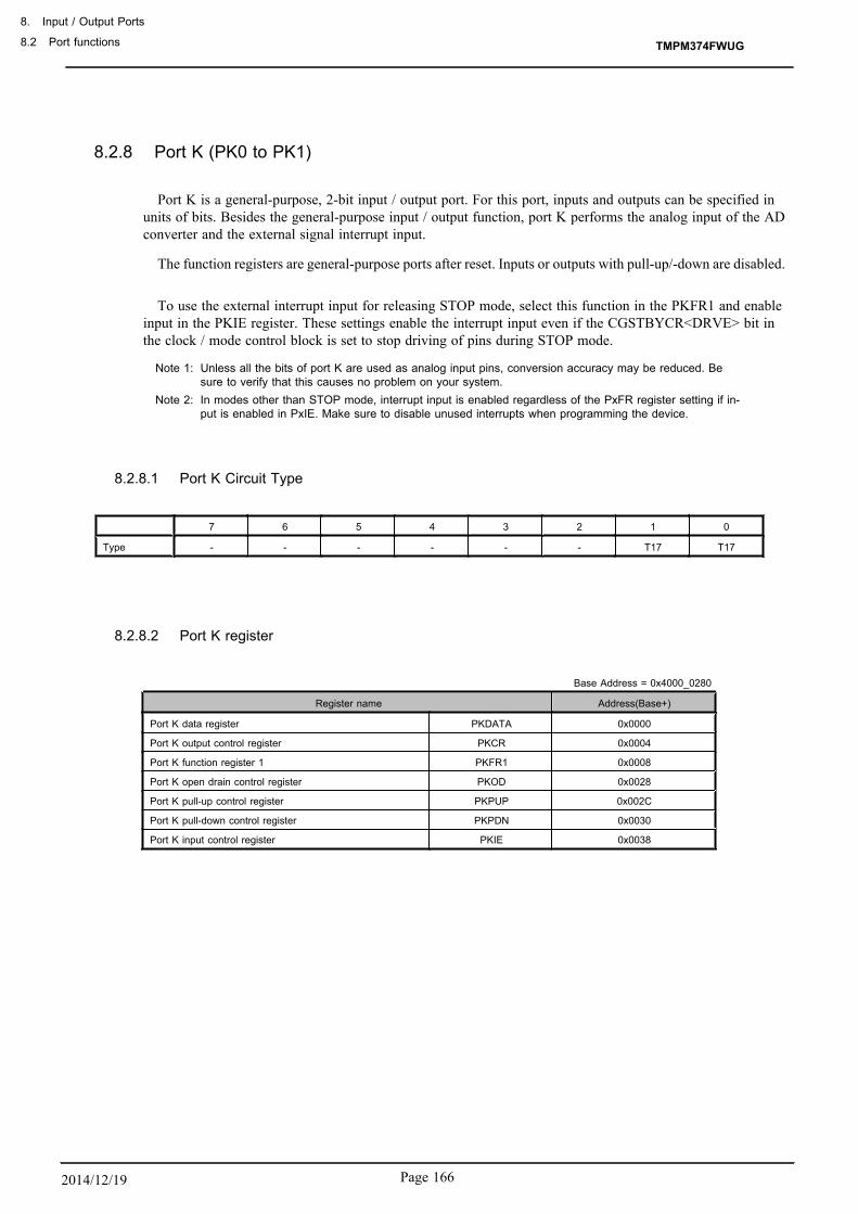
8.2.8 Port K (PK0 to PK1)
Port K is a general-purpose, 2-bit input / output port. For this port, inputs and outputs can be specified inunits of bits. Besides the general-purpose input / output function, port K performs the analog input of the ADconverter and the external signal interrupt input.
The function registers are general-purpose ports after reset. Inputs or outputs with pull-up/-down are disabled.
To use the external interrupt input for releasing STOP mode, select this function in the PKFR1 and enableinput in the PKIE register. These settings enable the interrupt input even if the CGSTBYCR<DRVE> bit inthe clock / mode control block is set to stop driving of pins during STOP mode.
Note 1: Unless all the bits of port K are used as analog input pins, conversion accuracy may be reduced. Besure to verify that this causes no problem on your system.
Note 2: In modes other than STOP mode, interrupt input is enabled regardless of the PxFR register setting if in-put is enabled in PxIE. Make sure to disable unused interrupts when programming the device.
8.2.8.1 Port K Circuit Type
7 6 5 4 3 2 1 0
Type - - - - - - T17 T17
8.2.8.2 Port K register
Base Address = 0x4000_0280
Register name Address(Base+)
Port K data register PKDATA 0x0000
Port K output control register PKCR 0x0004
Port K function register 1 PKFR1 0x0008
Port K open drain control register PKOD 0x0028
Port K pull-up control register PKPUP 0x002C
Port K pull-down control register PKPDN 0x0030
Port K input control register PKIE 0x0038
TMPM374FWUG
8. Input / Output Ports
8.2 Port functions
Page 1662014/12/19

8.2.8.3 PKDATA (Port K data register)
31 30 29 28 27 26 25 24
bit symbol - - - - - - - -
After reset 0 0 0 0 0 0 0 0
23 22 21 20 19 18 17 16
bit symbol - - - - - - - -
After reset 0 0 0 0 0 0 0 0
15 14 13 12 11 10 9 8
bit symbol - - - - - - - -
After reset 0 0 0 0 0 0 0 0
7 6 5 4 3 2 1 0
bit symbol - - - - - - PK1 PK0
After reset 0 0 0 0 0 0 0 0
Bit Bit Symbol Type Function
31-2 − R Read as 0.
1-0 PK1 to PK0 R/W Port K data register
8.2.8.4 PKCR (Port K output control register)
31 30 29 28 27 26 25 24
bit symbol - - - - - - - -
After reset 0 0 0 0 0 0 0 0
23 22 21 20 19 18 17 16
bit symbol - - - - - - - -
After reset 0 0 0 0 0 0 0 0
15 14 13 12 11 10 9 8
bit symbol - - - - - - - -
After reset 0 0 0 0 0 0 0 0
7 6 5 4 3 2 1 0
bit symbol - - - PK1C PK0C
After reset 0 0 0 0 0 0 0 0
Bit Bit Symbol Type Function
31-2 − R Read as 0.
1-0 PK1C to PK0C R/W Output0: Disable1: Enable
TMPM374FWUG
Page 167 2014/12/19
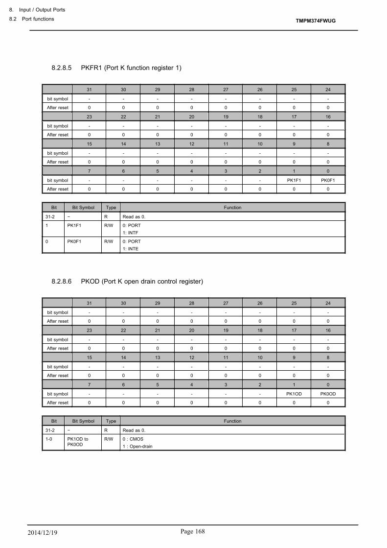
8.2.8.5 PKFR1 (Port K function register 1)
31 30 29 28 27 26 25 24
bit symbol - - - - - - - -
After reset 0 0 0 0 0 0 0 0
23 22 21 20 19 18 17 16
bit symbol - - - - - - - -
After reset 0 0 0 0 0 0 0 0
15 14 13 12 11 10 9 8
bit symbol - - - - - - - -
After reset 0 0 0 0 0 0 0 0
7 6 5 4 3 2 1 0
bit symbol - - - - - - PK1F1 PK0F1
After reset 0 0 0 0 0 0 0 0
Bit Bit Symbol Type Function
31-2 − R Read as 0.
1 PK1F1 R/W 0: PORT1: INTF
0 PK0F1 R/W 0: PORT1: INTE
8.2.8.6 PKOD (Port K open drain control register)
31 30 29 28 27 26 25 24
bit symbol - - - - - - - -
After reset 0 0 0 0 0 0 0 0
23 22 21 20 19 18 17 16
bit symbol - - - - - - - -
After reset 0 0 0 0 0 0 0 0
15 14 13 12 11 10 9 8
bit symbol - - - - - - - -
After reset 0 0 0 0 0 0 0 0
7 6 5 4 3 2 1 0
bit symbol - - - - - - PK1OD PK0OD
After reset 0 0 0 0 0 0 0 0
Bit Bit Symbol Type Function
31-2 − R Read as 0.
1-0 PK1OD toPK0OD
R/W 0 : CMOS1 : Open-drain
TMPM374FWUG
8. Input / Output Ports
8.2 Port functions
Page 1682014/12/19

8.2.8.7 PKPUP (Port K pull-up control register)
31 30 29 28 27 26 25 24
bit symbol - - - - - - - -
After reset 0 0 0 0 0 0 0 0
23 22 21 20 19 18 17 16
bit symbol - - - - - - - -
After reset 0 0 0 0 0 0 0 0
15 14 13 12 11 10 9 8
bit symbol - - - - - - - -
After reset 0 0 0 0 0 0 0 0
7 6 5 4 3 2 1 0
bit symbol - - - - - - PK1UP PK0UP
After reset 0 0 0 0 0 0 0 0
Bit Bit Symbol Type Function
31-2 − R Read as 0.
1-0 PK1UP toPK0UP
R/W Pull-up0: Disable1: Enable
8.2.8.8 PKPDN (Port K pull-down control register)
31 30 29 28 27 26 25 24
bit symbol - - - - - - - -
After reset 0 0 0 0 0 0 0 0
23 22 21 20 19 18 17 16
bit symbol - - - - - - - -
After reset 0 0 0 0 0 0 0 0
15 14 13 12 11 10 9 8
bit symbol - - - - - - - -
After reset 0 0 0 0 0 0 0 0
7 6 5 4 3 2 1 0
bit symbol - - - - - - PK1DN PK0DN
After reset 0 0 0 0 0 0 0 0
Bit Bit Symbol Type Function
31-2 − R Read as 0.
1-0 PK1DN toPK0DN
R/W Pull-down0: Disable1: Enable
TMPM374FWUG
Page 169 2014/12/19

8.2.8.9 PKIE (Port K input control register)
31 30 29 28 27 26 25 24
bit symbol - - - - - - - -
After reset 0 0 0 0 0 0 0 0
23 22 21 20 19 18 17 16
bit symbol - - - - - - - -
After reset 0 0 0 0 0 0 0 0
15 14 13 12 11 10 9 8
bit symbol - - - - - - - -
After reset 0 0 0 0 0 0 0 0
7 6 5 4 3 2 1 0
bit symbol - - - - - - PK1IE PK0IE
After reset 0 0 0 0 0 0 0 0
Bit Bit Symbol Type Function
31-2 − R Read as 0.
1-0 PK1IE toPK0IE
R/W Input0: Disable1: Enable
TMPM374FWUG
8. Input / Output Ports
8.2 Port functions
Page 1702014/12/19

8.2.9 Port M (PM0 to PM1)
Port M is a general-purpose, 2-bit input/output port. For this port, inputs and outputs can be specified inunits of bits. Besides the general-purpose input/output function, port M performs the high-speed oscillator1(X1 and X2) by CGOSCCR<HOSCON>=1.
While it become CGOSCCR<HOSCON>=1, each register of port M can not change to write. The proce-dure when it is used as an outside high-speed oscillator connection terminal look at a chapter of the "systemclock".(Note1)
The function registers are general-purpose ports after reset. Inputs or outputs with pull-up/-down are disabled.(Note2)
Note 1: If one of Port M registers except PMDATA and PMOD is not equal to the initial value, CGOSCCR<HO-SCON> can not be set to "1".
Note 2: The high-speed clock chosen after reset cancellation is a built-in high-speed clock. Therefore, in the ini-tial state, it become port M.
8.2.9.1 Port M Circuit Type
7 6 5 4 3 2 1 0
Type - - - - - - T21 T21
8.2.9.2 Port M register
Base Address = 0x4000_0300
Register name Address(Base+)
Port M data register PMDATA 0x0000
Port M output control register PMCR 0x0004
Port M open drain control register PMOD 0x0028
Port M pull-up control register PMPUP 0x002C
Port M pull-down control register PMPDN 0x0030
Port M input control register PMIE 0x0038
TMPM374FWUG
Page 171 2014/12/19

8.2.9.3 PMDATA (Port M data register)
31 30 29 28 27 26 25 24
bit symbol - - - - - - - -
After reset 0 0 0 0 0 0 0 0
23 22 21 20 19 18 17 16
bit symbol - - - - - - - -
After reset 0 0 0 0 0 0 0 0
15 14 13 12 11 10 9 8
bit symbol - - - - - - - -
After reset 0 0 0 0 0 0 0 0
7 6 5 4 3 2 1 0
bit symbol - - - - - - PM1 PM0
After reset 0 0 0 0 0 0 0 0
Bit Bit Symbol Type Function
31-2 − R Read as 0.
1-0 PM1 to PM0 R/W Port M data register
8.2.9.4 PMCR (Port M output control register)
31 30 29 28 27 26 25 24
bit symbol - - - - - - - -
After reset 0 0 0 0 0 0 0 0
23 22 21 20 19 18 17 16
bit symbol - - - - - - - -
After reset 0 0 0 0 0 0 0 0
15 14 13 12 11 10 9 8
bit symbol - - - - - - - -
After reset 0 0 0 0 0 0 0 0
7 6 5 4 3 2 1 0
bit symbol - - - - - - PM1C PM0C
After reset 0 0 0 0 0 0 0 0
Bit Bit Symbol Type Function
31-2 − R Read as 0.
1-0 PM1C to PM0C R/W Output0: Disable1: Enable
TMPM374FWUG
8. Input / Output Ports
8.2 Port functions
Page 1722014/12/19

8.2.9.5 PMOD (Port M open drain control register)
31 30 29 28 27 26 25 24
bit symbol - - - - - - - -
After reset 0 0 0 0 0 0 0 0
23 22 21 20 19 18 17 16
bit symbol - - - - - - - -
After reset 0 0 0 0 0 0 0 0
15 14 13 12 11 10 9 8
bit symbol - - - - - - - -
After reset 0 0 0 0 0 0 0 0
7 6 5 4 3 2 1 0
bit symbol - - - - - - PM1OD PM0OD
After reset 0 0 0 0 0 0 0 0
Bit Bit Symbol Type Function
31-2 − R Read as 0.
1-0 PM1OD toPM0OD
R/W 0 : CMOS1 : Open-drain
8.2.9.6 PMPUP (Port M pull-up control register)
31 30 29 28 27 26 25 24
bit symbol - - - - - - - -
After reset 0 0 0 0 0 0 0 0
23 22 21 20 19 18 17 16
bit symbol - - - - - - - -
After reset 0 0 0 0 0 0 0 0
15 14 13 12 11 10 9 8
bit symbol - - - - - - - -
After reset 0 0 0 0 0 0 0 0
7 6 5 4 3 2 1 0
bit symbol - - - - - - PM1UP PM0UP
After reset 0 0 0 0 0 0 0 0
Bit Bit Symbol Type Function
31-2 − R Read as 0.
1-0 PM1UP toPM0UP
R/W Pull-up0: Disable1: Enable
TMPM374FWUG
Page 173 2014/12/19
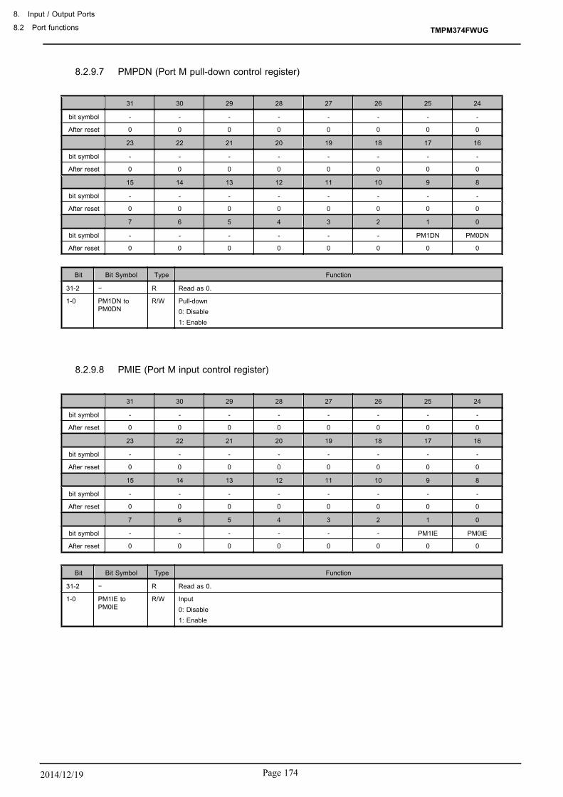
8.2.9.7 PMPDN (Port M pull-down control register)
31 30 29 28 27 26 25 24
bit symbol - - - - - - - -
After reset 0 0 0 0 0 0 0 0
23 22 21 20 19 18 17 16
bit symbol - - - - - - - -
After reset 0 0 0 0 0 0 0 0
15 14 13 12 11 10 9 8
bit symbol - - - - - - - -
After reset 0 0 0 0 0 0 0 0
7 6 5 4 3 2 1 0
bit symbol - - - - - - PM1DN PM0DN
After reset 0 0 0 0 0 0 0 0
Bit Bit Symbol Type Function
31-2 − R Read as 0.
1-0 PM1DN toPM0DN
R/W Pull-down0: Disable1: Enable
8.2.9.8 PMIE (Port M input control register)
31 30 29 28 27 26 25 24
bit symbol - - - - - - - -
After reset 0 0 0 0 0 0 0 0
23 22 21 20 19 18 17 16
bit symbol - - - - - - - -
After reset 0 0 0 0 0 0 0 0
15 14 13 12 11 10 9 8
bit symbol - - - - - - - -
After reset 0 0 0 0 0 0 0 0
7 6 5 4 3 2 1 0
bit symbol - - - - - - PM1IE PM0IE
After reset 0 0 0 0 0 0 0 0
Bit Bit Symbol Type Function
31-2 − R Read as 0.
1-0 PM1IE toPM0IE
R/W Input0: Disable1: Enable
TMPM374FWUG
8. Input / Output Ports
8.2 Port functions
Page 1742014/12/19
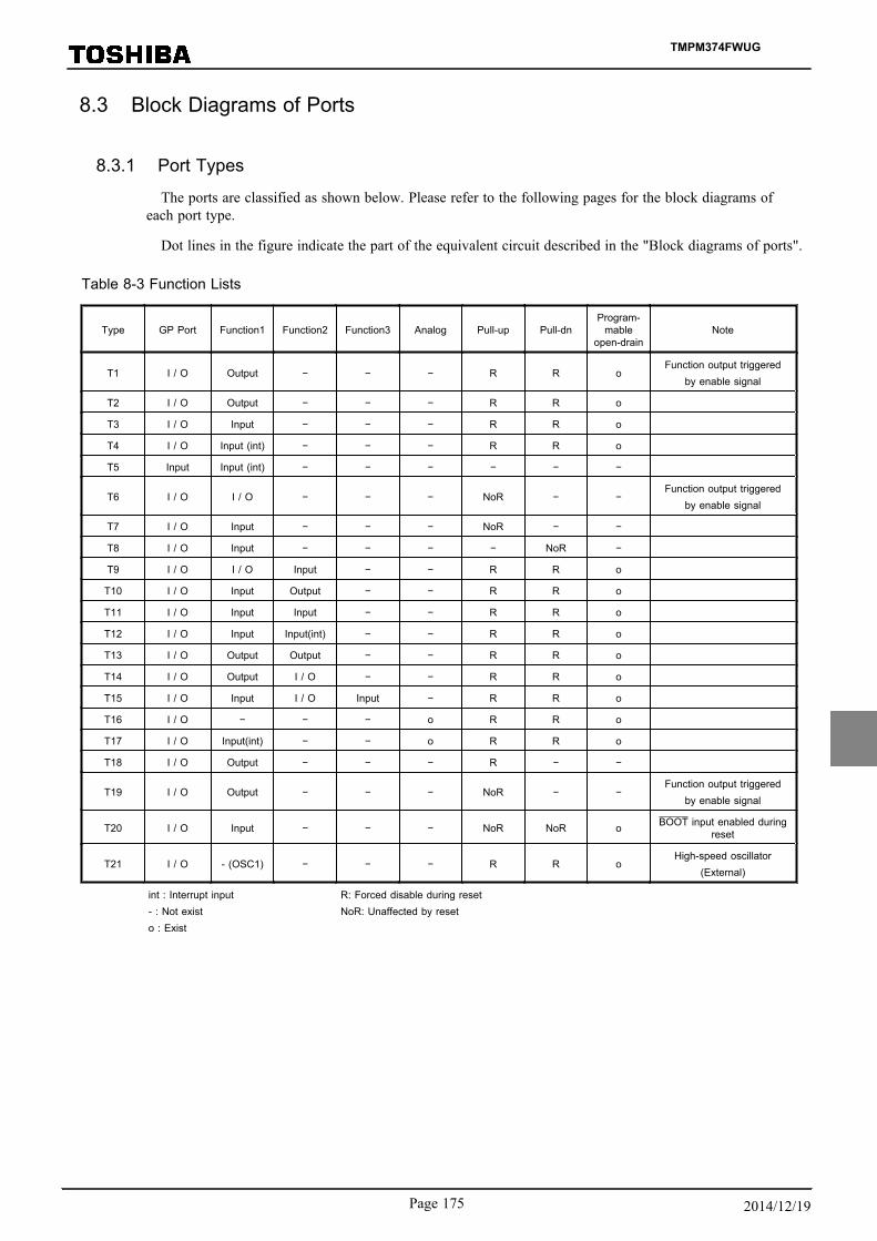
8.3 Block Diagrams of Ports
8.3.1 Port Types
The ports are classified as shown below. Please refer to the following pages for the block diagrams ofeach port type.
Dot lines in the figure indicate the part of the equivalent circuit described in the "Block diagrams of ports".
Table 8-3 Function Lists
Type GP Port Function1 Function2 Function3 Analog Pull-up Pull-dnProgram-
mableopen-drain
Note
T1 I / O Output − − − R R οFunction output triggered
by enable signal
T2 I / O Output − − − R R ο
T3 I / O Input − − − R R ο
T4 I / O Input (int) − − − R R ο
T5 Input Input (int) − − − − − −
T6 I / O I / O − − − NoR − −Function output triggered
by enable signal
T7 I / O Input − − − NoR − −
T8 I / O Input − − − − NoR −
T9 I / O I / O Input − − R R ο
T10 I / O Input Output − − R R ο
T11 I / O Input Input − − R R ο
T12 I / O Input Input(int) − − R R ο
T13 I / O Output Output − − R R ο
T14 I / O Output I / O − − R R ο
T15 I / O Input I / O Input − R R ο
T16 I / O − − − ο R R ο
T17 I / O Input(int) − − ο R R ο
T18 I / O Output − − − R − −
T19 I / O Output − − − NoR − −Function output triggered
by enable signal
T20 I / O Input − − − NoR NoR ο BOOT input enabled duringreset
T21 I / O - (OSC1) − − − R R οHigh-speed oscillator
(External)
int : Interrupt input- : Not existo : Exist
R: Forced disable during resetNoR: Unaffected by reset
TMPM374FWUG
Page 175 2014/12/19

8.3.2 Type T1
PxPUP(Pull-up Control)
I /OPORT
Port Read
0
1
1
0
RESET
Drive Disablein STOP Mode(Set by <DRVE>)
PxIE(Input Control)
PxOD(Open Drain
Control)
PxDATA(Output Latch)
PxFR1(Function Control)
PxCR(Output Control)
PxPDN(Pull-down
Control)
FunctionOutput
0
1
FunctionOutputEnableInternal D
ata Bus
Programablepull-up and pull-down
Figure 8-1 Port Type T1
TMPM374FWUG
8. Input / Output Ports
8.3 Block Diagrams of Ports
Page 1762014/12/19

8.3.3 Type T2
PxPUP(Pull-up Control)
Port Read
0
1
RESET
PxIE(Input Control)
PxOD(Open Drain
Control)
PxDATA(Output Latch)
PxFR1(Function Control)
PxCR(Output Controll)
PxPDN(Pull-down
Control)
FunctionOutput
0
1
Internal Data B
us
I /OPORT
Programablepull-up and pull-down
Drive Disablein STOP Mode(Set by <DRVE>)
Figure 8-2 PORT Type T2
TMPM374FWUG
Page 177 2014/12/19

8.3.4 Type T3
PxPUP(Pull-up Control)
0
1
RESET
PxIE(Input Control)
PxOD(Open Drain
Control)
PxDATA(Output Latch)
PxFR1(Function Control)
PxCR(Output Controll)
PxPDN(Pull-down
Control)
Port Read
I /OPORT
Programablepull-up and pull-down
Drive Disablein STOP Mode(Set by <DRVE>)
Internal Data B
us
FunctionInput1
Figure 8-3 PORT Type T3
TMPM374FWUG
8. Input / Output Ports
8.3 Block Diagrams of Ports
Page 1782014/12/19

8.3.5 Type T4
PxPUP(Pull-up Control)
0
1
RESET
PxIE(Input Control)
PxOD(Open Drain
Control)
PxDATA(Output Latch)
PxFR1(Function Control)
PxCR(Output Controll)
PxPDN(Pull-down
Control)
Internal Data B
us
Port Read
I /OPORT
Drive Disablein STOP Mode(Set by <DRVE>)
Programablepull-up and pull-down
Figure 8-4 PORT Type T4
TMPM374FWUG
Page 179 2014/12/19

8.3.6 Type T5
0
1
PxIE(Input Control)
PxFR1(Function Control)
I /OPORT
Drive Disablein STOP Mode(Set by <DRVE>)
Internal Data B
us
Port Read
Figure 8-5 PORT Type T5
TMPM374FWUG
8. Input / Output Ports
8.3 Block Diagrams of Ports
Page 1802014/12/19

8.3.7 Type T6
PxPUP(Pull-up Control)
0
1
1
0
PxIE(Input Control)
PxDATA(Output Latch)
PxFR1(Function Control)
PxCR(Output Controll)
0
1
1
0
Port Read
FunctionOutput
FunctionOutputEnable
I /OPORT
Drive Disablein STOP Mode(Set by <DRVE>)
Programablepull-up
Internal Data B
us
Figure 8-6 PORT Type T6
TMPM374FWUG
Page 181 2014/12/19
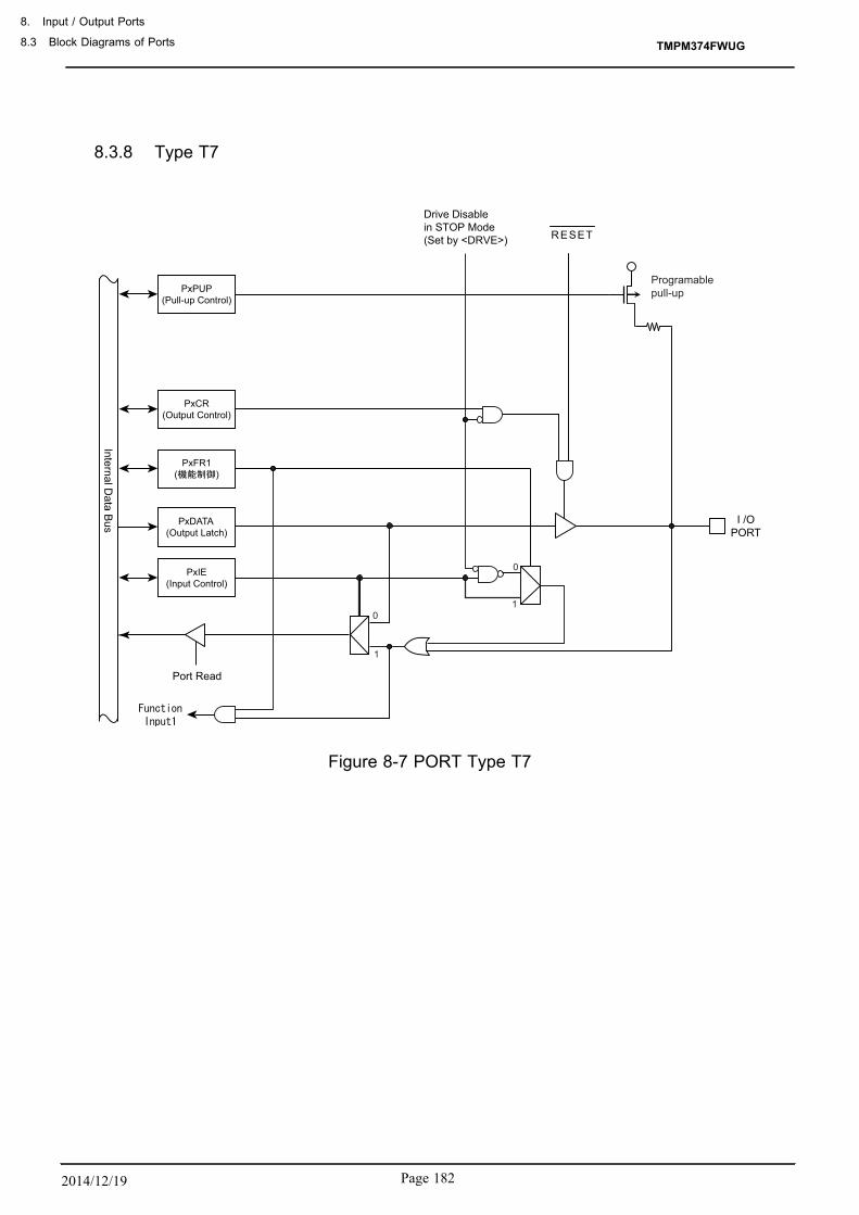
8.3.8 Type T7
PxPUP(Pull-up Control)
0
1
PxIE(Input Control)
PxDATA(Output Latch)
PxFR1( )
PxCR(Output Control)
1
0
RESET
Port Read
I /OPORT
Drive Disablein STOP Mode(Set by <DRVE>)
Programablepull-up
Internal Data B
usFigure 8-7 PORT Type T7
TMPM374FWUG
8. Input / Output Ports
8.3 Block Diagrams of Ports
Page 1822014/12/19

8.3.9 Type T8
0
1
PxIE(Input Control)
PxDATA(Output Latch)
PxFR1( )
PxCR(Output Control)
1
0
RESET
PxPDN(Pull-down
Control)
Internal Data B
us
Port Read
I /OPORT
Drive Disablein STOP Mode(Set by <DRVE>)
Programablepull-down
Figure 8-8 PORT Type T8
TMPM374FWUG
Page 183 2014/12/19
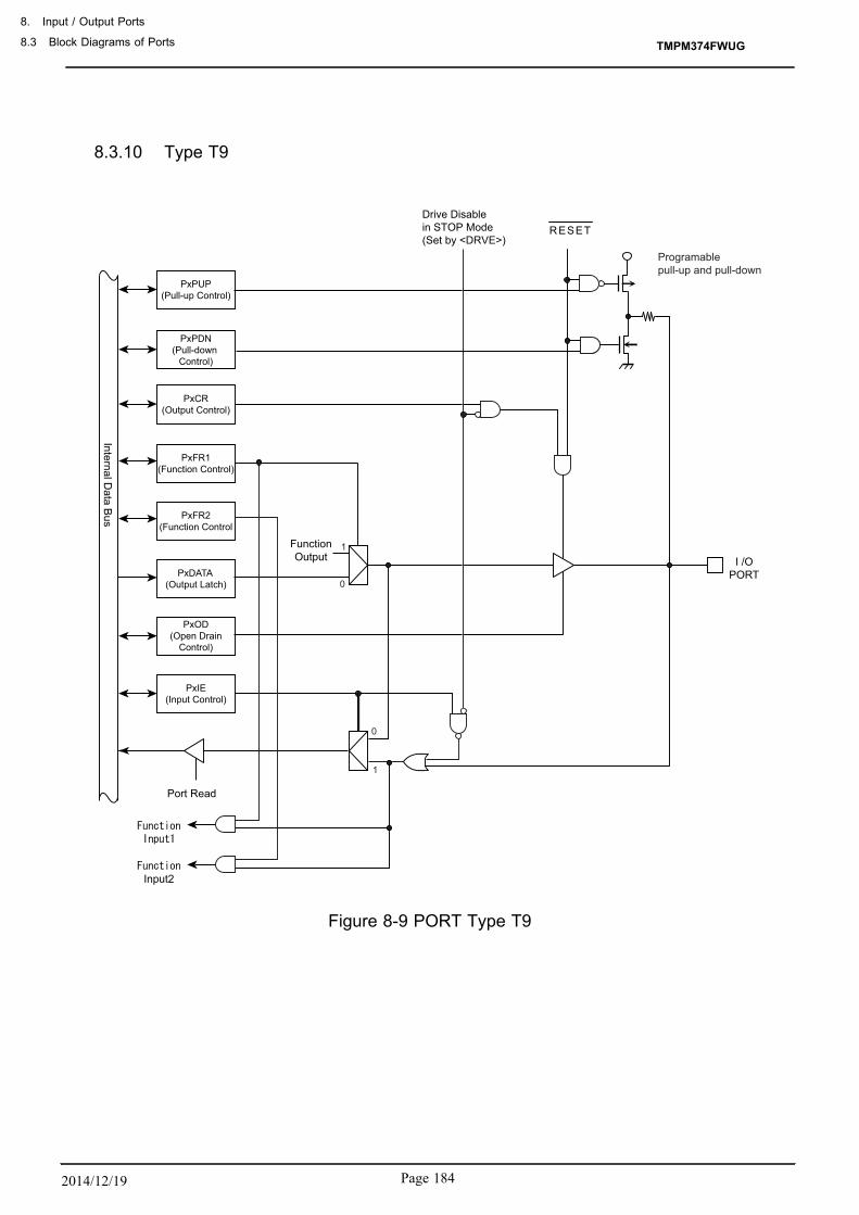
8.3.10 Type T9
PxPUP(Pull-up Control)
0
1
RESET
PxIE(Input Control)
PxOD(Open Drain
Control)
PxDATA(Output Latch)
PxFR1(Function Control)
PxCR(Output Control)
PxPDN(Pull-down
Control)
0
1
PxFR2(Function Control
Input2
I /OPORT
Drive Disablein STOP Mode(Set by <DRVE>)
Programablepull-up and pull-down
Internal Data B
us
FunctionOutput
Port Read
Figure 8-9 PORT Type T9
TMPM374FWUG
8. Input / Output Ports
8.3 Block Diagrams of Ports
Page 1842014/12/19

8.3.11 Type T10
PxPUP(Pull-up Control)
0
1
RESET
PxIE(Input Control)
PxOD(Open Drain
Control)
PxDATA(Output Latch)
PxFR1(Function Control)
PxCR(Output Control)
PxPDN(Pull-down
Control)
0
1
1
PxFR2(Function Control)
I /OPORT
Drive Disablein STOP Mode(Set by <DRVE>)
Programablepull-up and pull-down
Internal Data B
us
Port Read
FunctionOutput
Figure 8-10 PORT Type T10
TMPM374FWUG
Page 185 2014/12/19

8.3.12 Type T11
PxPUP(Pull-up Control)
0
1
RESET
PxIE(Input Control)
PxOD(Open Drain
Control)
PxDATA(Output Latch)
PxFR1(Function Control)
PxCR(Output Control)
PxPDN(Pull-down
Control)
1
PxFR2(Function Control)
Input2
Internal Data B
us
Port Read
I /OPORT
Drive Disablein STOP Mode(Set by <DRVE>)
Programablepull-up and pull-down
Figure 8-11 PORT Type T11
TMPM374FWUG
8. Input / Output Ports
8.3 Block Diagrams of Ports
Page 1862014/12/19
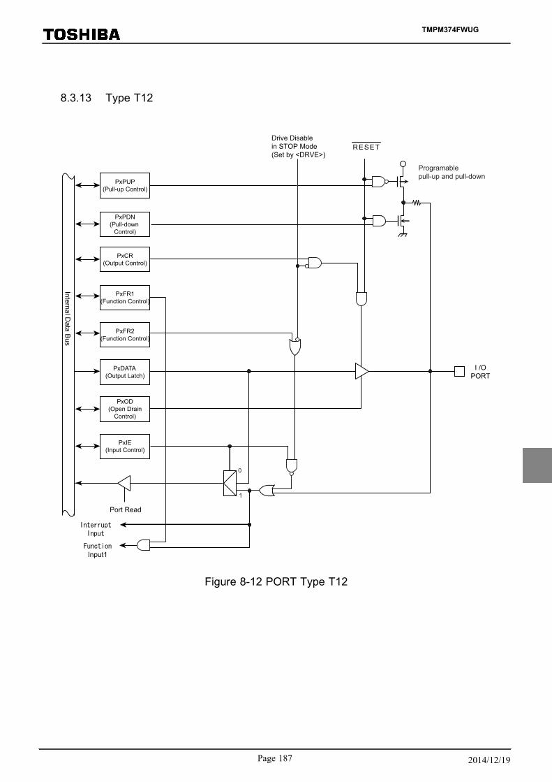
8.3.13 Type T12
PxPUP(Pull-up Control)
0
1
RESET
PxIE(Input Control)
PxOD(Open Drain
Control)
PxDATA(Output Latch)
PxFR1(Function Control)
PxCR(Output Control)
PxPDN(Pull-down
Control)
Input1
PxFR2(Function Control)
I /OPORT
Drive Disablein STOP Mode(Set by <DRVE>)
Programablepull-up and pull-down
Port Read
Internal Data B
us
Figure 8-12 PORT Type T12
TMPM374FWUG
Page 187 2014/12/19
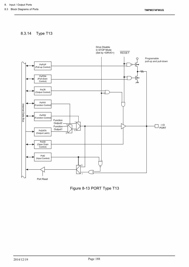
8.3.14 Type T13
PxPUP(Pull-up Control)
0
1
RESET
PxIE(Input Control)
PxOD(Open Drain
Control)
PxDATA(Output Latch)
PxFR1(Function Control)
PxCR(Output Control)
PxPDN(Pull-down
Control)
0
1
PxFR2(Function Control)
0
1
Internal Data B
us
FunctionOutput1
FunctionOutput2
Port Read
I /OPORT
Drive Disablein STOP Mode(Set by <DRVE>)
Programablepull-up and pull-down
Figure 8-13 PORT Type T13
TMPM374FWUG
8. Input / Output Ports
8.3 Block Diagrams of Ports
Page 1882014/12/19

8.3.15 Type T14
PxPUP(Pull-up Control)
0
1
RESET
PxIE(Input Control)
PxOD(Open Drain
Control)
PxDATA(Output Latch)
PxFR1(Function Control)
PxCR(Output Control)
PxPDN(Pull-down
Control)
PxFR2(Function Control)
0
1
Internal Data B
us
FunctionOutput
Port Read
I /OPORT
Drive Disablein STOP Mode(Set by <DRVE>)
Programablepull-up and pull-down
Figure 8-14 PORT Type T14
TMPM374FWUG
Page 189 2014/12/19

8.3.16 Type T15
PxPUP(Pull-up Control)
0
1
RESET
PxIE(Input Control)
PxOD(Open Drain
Contro)
PxDATA(Output Latch)
PxFR1(Function Control)
PxCR(Output Control)
PxPDN(Pull-down
Control)
0
1
1
PxFR2(Function Control)
PxFR3(Function Control)
2
3
I /OPORT
Drive Disablein STOP Mode(Set by <DRVE>)
Programablepull-up and pull-down
Internal Data B
us
FunctionOutput2
Port Read
Figure 8-15 PORT Type T15
TMPM374FWUG
8. Input / Output Ports
8.3 Block Diagrams of Ports
Page 1902014/12/19

8.3.17 Type T16
PxPUP(Pull-up Control)
0
1
RESET
PxIE(Input Control)
PxOD(Open Drain
Control)
PxDATA(Output Latch)
PxCR(Output Control)
PxPDN(Pull-down
Control)
Analog Input
Internal Data B
usPort Read
I /OPORT
Drive Disablein STOP Mode(Set by <DRVE>)
Programablepull-up and pull-down
Figure 8-16 PORT Type T16
TMPM374FWUG
Page 191 2014/12/19

8.3.18 Type T17
PxPUP(Pull-up Control)
0
1
RESET
PxIE(Input Control)
PxOD(Open Drain
Control)
PxDATA(Output Latch)
PxFR1(Function Control)
PxCR(Output Control)
PxPDN(Pull-down
Control)
Interrupt Input
Analog Input
I /OPORT
Drive Disablein STOP Mode(Set by <DRVE>)
Programablepull-up and pull-down
Internal Data B
us
Port Read
Figure 8-17 PORT Type T17
TMPM374FWUG
8. Input / Output Ports
8.3 Block Diagrams of Ports
Page 1922014/12/19

8.3.19 Type T18
PxPUP(Pull-up Control)
0
1
1
0
PxIE(Input Control)
PxDATA(Output Latch)
PxFR1(Function Control)
PxCR(Output Control)
0
1
RESET
Port Read
Internal Data B
us
FunctionOutput1 I /O
PORT
Drive Disablein STOP Mode(Set by <DRVE>)
Programablepull-up and pull-down
Figure 8-18 PORT Type T18
TMPM374FWUG
Page 193 2014/12/19
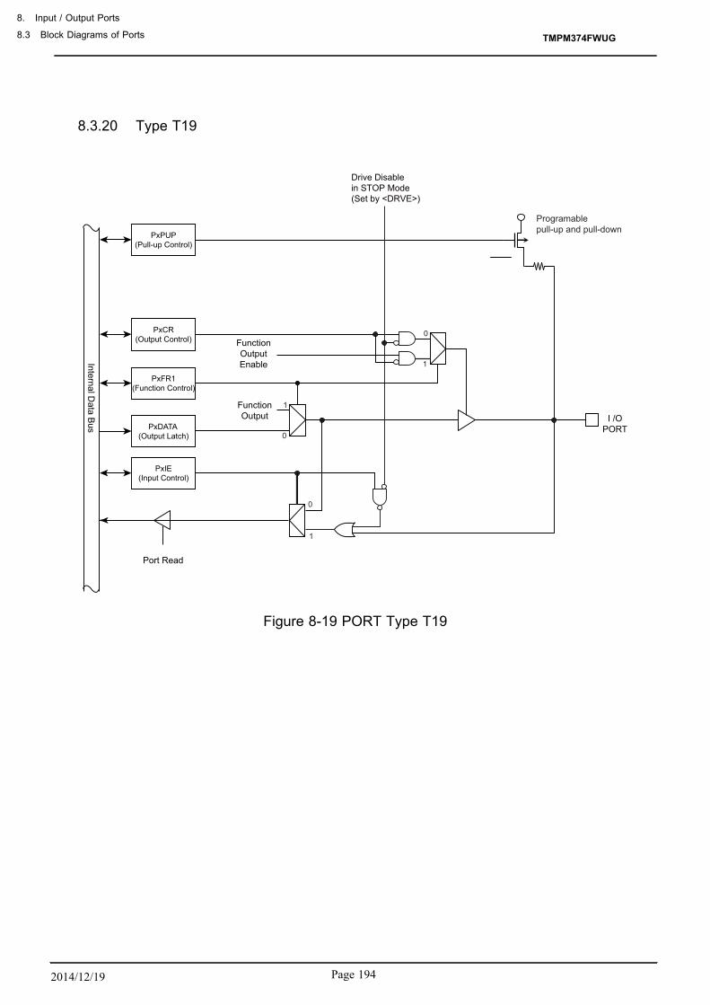
8.3.20 Type T19
PxPUP(Pull-up Control)
1
0
PxIE(Input Control)
PxDATA(Output Latch)
PxFR1(Function Control)
PxCR(Output Control)
0
1
0
1
I /OPORT
Drive Disablein STOP Mode(Set by <DRVE>)
Programablepull-up and pull-down
Port Read
Internal Data B
us
FunctionOutput
FunctionOutputEnable
Figure 8-19 PORT Type T19
TMPM374FWUG
8. Input / Output Ports
8.3 Block Diagrams of Ports
Page 1942014/12/19

8.3.21 Type T20
PxPUP(Pull-up Control)
0
1
PxIE(Input Control))
PxOD(Open Drain
Control)
PxDATA(Output Latch)
PxFR1(Function Control)
PxCR(Output Control)
PxPDN(Pull-down
Control)
1
BOOT
Port Read
Internal Data B
us
I /OPORT
Drive Disablein STOP Mode(Set by <DRVE>)
Programablepull-up and pull-down
Input fromthe RESET pin
TMPM374FWUG
Page 195 2014/12/19

8.3.22 Type T21
PxPUP(Pull-up Control)
0
1
RESET
PxIE(Input Control)
PxOD(Open Drain
Control)
PxDATA(Output Latch)
PxCR(Output Control)
PxPDN(Pull-down
Control)
External high-speedOscillator
Port Read
Internal Data B
us
I /OPORT
Drive Disablein STOP Mode(Set by <DRVE>)
Programablepull-up and pull-down
TMPM374FWUG
8. Input / Output Ports
8.3 Block Diagrams of Ports
Page 1962014/12/19

8.4 Appendix Port Setting ListThe following table shows the register setting for each function.
Initialization of the ports where the [・]does not exist in the "After reset" field is set to "0" for all register settings.
Setting for the bit "x" can be arbitrarily-specified.
8.4.1 Port A Setting
Table 8-4 Port Setting List (Port A)
PinPortType
FunctionAfterreset
PACR PAFR1 PAFR2 PAOD PAPUP PAPDN PAIE
PA4 T9
Input Port 0 0 0 x x x 1
Output Port 1 0 0 x x x 0
SCLK1 (I / O) 1 1 0 x x x 1
CTS1 (Input) 0 0 1 x x x 1
PA5 T13
Input Port 0 0 0 x x x 1
Output Port 1 0 0 x x x 0
TXD1 (Output) 1 1 0 x x x 0
TB6OUT(Output) 1 0 1 x x x 0
PA6 T11
Input Port 0 0 0 x x x 1
Output Port 1 0 0 x x x 0
RXD1 (Input) 0 1 0 x x x 1
TB6IN (Input) 0 0 1 x x x 1
TMPM374FWUG
Page 197 2014/12/19

8.4.2 Port B Setting
Table 8-5 Port Setting List (Port B)
PinPortType
FunctionAfterreset
PBCR PBFR1 PBOD PBPUP PBPDN PBIE
PB3 T6
Input Port 0 0 x x x 1
Output Port 1 0 x x x 0
TMS / SWDIO (I / O) 1 1 0 1 0 1
PB4 T8
Input Port 0 0 x x x 1
Output Port 1 0 x x x 0
TCK / SWCLK (Input) 0 1 0 0 1 1
PB5 T19
Input Port 0 0 x x x 1
Output Port 1 0 x x x 0
TDO / SWV (Output) 1 1 0 0 0 0
PB6 T7
Input Port 0 0 x x x 1
Output Port 1 0 x x x 0
TDI (Input) 0 1 0 1 0 1
TMPM374FWUG
8. Input / Output Ports
8.4 Appendix Port Setting List
Page 1982014/12/19

8.4.3 Port E Setting
Table 8-6 Port Setting List (Port E)
PinPortType
FunctionAfterreset
PECR PEFR1 PEFR2 PEOD PEPUP PEPDN PEIE
PE0 T2
Input Port 0 0 - x x x 1
Output Port 1 0 - x x x 0
TXD0 (Output) 1 1 - x x x 0
PE1 T3
Input Port 0 0 - x x x 1
Output Port 1 0 - x x x 0
RXD0 (Input) 0 1 - x x x 1
PE2 T9
Input Port 0 0 0 x x x 1
Output Port 1 0 0 x x x 0
SCLK0 (I / O) 1 1 0 x x x 1
CTS0 (Input) 0 0 1 x x x 1
PE4 T12
Input Port 0 0 0 x x x 1
Output Port 1 0 0 x x x 0
TB2IN (Input) 0 1 0 x x x 1
INT5 (Input) 0 0 1 x x x 1
PE6 T12
Input Port 0 0 0 x x x 1
Output Port 1 0 0 x x x 0
TB3IN (Input) 0 1 0 x x x 1
INT6 (Input) 0 0 1 x x x 1
PE7 T14
Input Port 0 0 0 x x x 1
Output Port 1 0 0 x x x 0
TB3OUT (Output) 1 1 0 x x x 0
INT7 (Input) 0 0 1 x x x 1
TMPM374FWUG
Page 199 2014/12/19
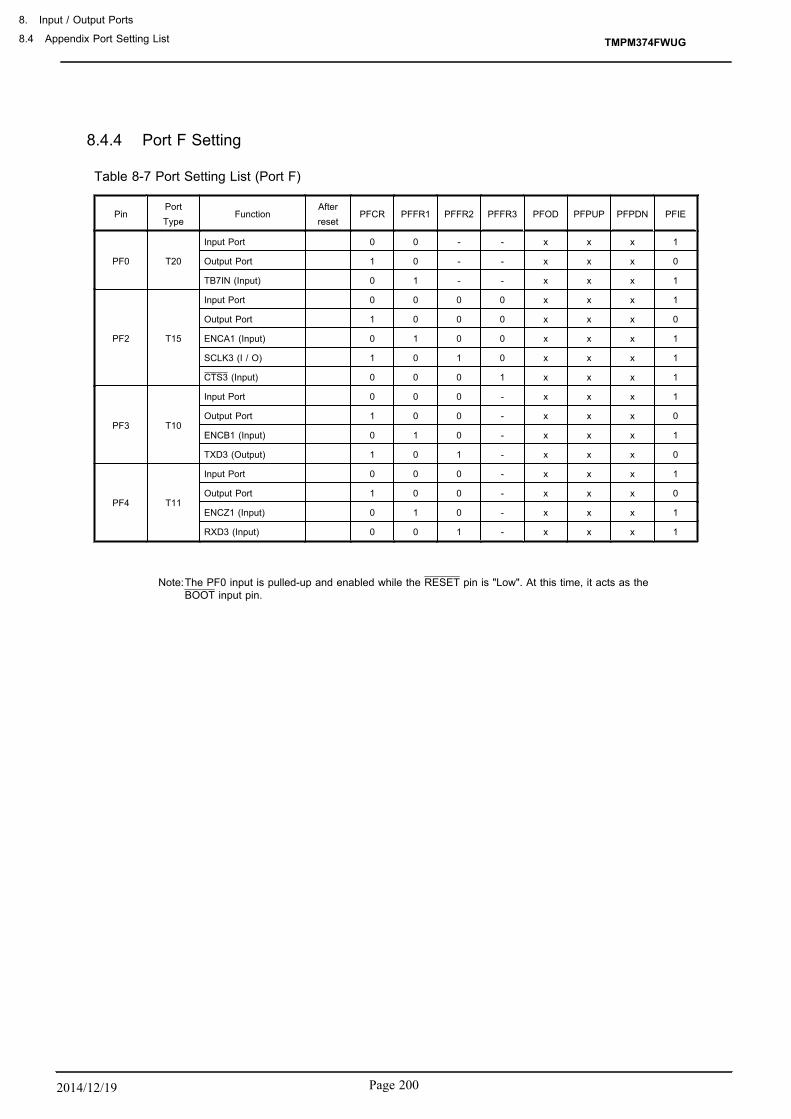
8.4.4 Port F Setting
Table 8-7 Port Setting List (Port F)
PinPortType
FunctionAfterreset
PFCR PFFR1 PFFR2 PFFR3 PFOD PFPUP PFPDN PFIE
PF0 T20
Input Port 0 0 - - x x x 1
Output Port 1 0 - - x x x 0
TB7IN (Input) 0 1 - - x x x 1
PF2 T15
Input Port 0 0 0 0 x x x 1
Output Port 1 0 0 0 x x x 0
ENCA1 (Input) 0 1 0 0 x x x 1
SCLK3 (I / O) 1 0 1 0 x x x 1
CTS3 (Input) 0 0 0 1 x x x 1
PF3 T10
Input Port 0 0 0 - x x x 1
Output Port 1 0 0 - x x x 0
ENCB1 (Input) 0 1 0 - x x x 1
TXD3 (Output) 1 0 1 - x x x 0
PF4 T11
Input Port 0 0 0 - x x x 1
Output Port 1 0 0 - x x x 0
ENCZ1 (Input) 0 1 0 - x x x 1
RXD3 (Input) 0 0 1 - x x x 1
Note:The PF0 input is pulled-up and enabled while the RESET pin is "Low". At this time, it acts as theBOOT input pin.
TMPM374FWUG
8. Input / Output Ports
8.4 Appendix Port Setting List
Page 2002014/12/19

8.4.5 Port G Setting
Table 8-8 Port Setting List (Port G)
PinPortType
FunctionAfterreset
PGCR PGFR1 PGOD PGPUP PGPDN PGIE
PG0 T1
Input Port 0 0 x x x 1
Output Port 1 0 x x x 0
UO1 (Output) 1 1 x x x 0
PG1 T1
Input Port 0 0 x x x 1
Output Port 1 0 x x x 0
XO1 (Output) 1 1 x x x 0
PG2 T1
Input Port 0 0 x x x 1
Output Port 1 0 x x x 0
VO1 (Output) 1 1 x x x 0
PG3 T1
Input Port 0 0 x x x 1
Output Port 1 0 x x x 0
YO1 (Output) 1 1 x x x 0
PG4 T1
Input Port 0 0 x x x 1
Output Port 1 0 x x x 0
WO1 (Output) 1 1 x x x 0
PG5 T1
Input Port 0 0 x x x 1
Output Port 1 0 x x x 0
ZO1 (Output) 1 1 x x x 0
PG6 T3
Input Port 0 0 x x x 1
Output Port 1 0 x x x 0
EMG1 (Input) 0 1 x x x 1
PG7 T3
Input Port 0 0 x x x 1
Output Port 1 0 x x x 0
OVV1 (Input) 0 1 x x x 1
TMPM374FWUG
Page 201 2014/12/19

8.4.6 Port I Setting
Table 8-9 Port Setting List (Port I)
PinPortType
FunctionAfterreset
PICR PIOD PIPUP PIPDN PIIE
PI3 T16
Input Port 0 x x x 1
Output Port 1 x x x 0
Analog Input 0 0 0 0 0
TMPM374FWUG
8. Input / Output Ports
8.4 Appendix Port Setting List
Page 2022014/12/19

8.4.7 Port J Setting
Table 8-10 Port Setting List (Port J)
PinPortType
FunctionAfterreset
PJCR PJFR1 PJOD PJPUP PJPDN PJIE
PJ0 T16
Input Port 0 - x x x 1
Output Port 1 - x x x 0
Analog Input 0 - 0 0 0 0
PJ6 T17
Input Port 0 0 x x x 1
Output Port 1 0 x x x 0
Analog Input 0 0 0 0 0 0
INTC (Input) 0 1 x x x 1
PJ7 T17
Input Port 0 0 x x x 1
Output Port 1 0 x x x 0
Analog Input 0 0 0 0 0 0
INTD (Input) 0 1 x x x 1
TMPM374FWUG
Page 203 2014/12/19

8.4.8 Port K Setting
Table 8-11 Port Setting List (Port K)
PinPortType
FunctionAfterreset
PKCR PKFR1 PKOD PKPUP PKPDN PKIE
PK0 T17
Input Port 0 0 x x x 1
Output Port 1 0 x x x 0
Analog Input 0 0 0 0 0 0
INTE (Input) 0 1 x x x 1
PK1 T17
Input Port 0 0 x x x 1
Output Port 1 0 x x x 0
Analog Input 0 0 0 0 0 0
INTF (Input) 0 1 x x x 1
8.4.9 Port M Setting
Table 8-12 Port Setting List (Port M)
PinPortType
FunctionAfterreset
PMCR PMOD PMPUP PMPDN PMIE
PM0 T21Input Port 0 x x x 1
Output Port 1 x x x 0
PM1 T21Input Port 0 x x x 1
Output Port 1 x x x 0
Note:X1,X2 exist
TMPM374FWUG
8. Input / Output Ports
8.4 Appendix Port Setting List
Page 2042014/12/19
9. 16-bit Timer / Event Counters (TMRB)
9.1 OutlineTMRB operate in the following four operation modes:
・ 16-bit interval timer mode・ 16-bit event counter mode・ 16-bit programmable pulse generation mode (PPG)・ External trigger Programmable pulse generation mode (PPG)
The use of the capture function allows TMRB to perform the following two measurements.
・ One shot pulse output by an external trigger・ Pulse width measurement
In the following explanation of this section, "x" indicates a channel number.
TMPM374FWUG
Page 205 2014/12/19
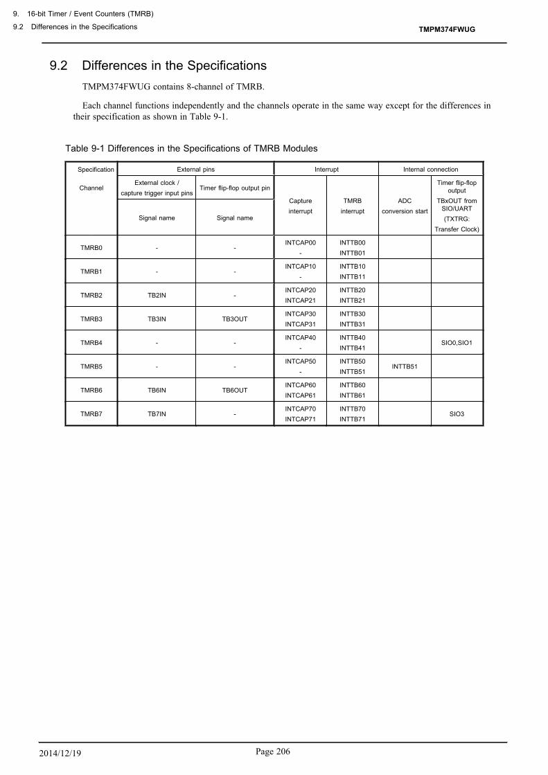
9.2 Differences in the SpecificationsTMPM374FWUG contains 8-channel of TMRB.
Each channel functions independently and the channels operate in the same way except for the differences intheir specification as shown in Table 9-1.
Table 9-1 Differences in the Specifications of TMRB Modules
Specification External pins Interrupt Internal connection
ChannelExternal clock /
capture trigger input pinsTimer flip-flop output pin
Captureinterrupt
TMRBinterrupt
ADCconversion start
Timer flip-flopoutput
TBxOUT fromSIO/UART(TXTRG:
Transfer Clock)
Signal name Signal name
TMRB0 - -INTCAP00
-INTTB00INTTB01
TMRB1 - -INTCAP10
-INTTB10INTTB11
TMRB2 TB2IN -INTCAP20INTCAP21
INTTB20INTTB21
TMRB3 TB3IN TB3OUTINTCAP30INTCAP31
INTTB30INTTB31
TMRB4 - -INTCAP40
-INTTB40INTTB41
SIO0,SIO1
TMRB5 - -INTCAP50
-INTTB50INTTB51
INTTB51
TMRB6 TB6IN TB6OUTINTCAP60INTCAP61
INTTB60INTTB61
TMRB7 TB7IN -INTCAP70INTCAP71
INTTB70INTTB71
SIO3
TMPM374FWUG
9. 16-bit Timer / Event Counters (TMRB)
9.2 Differences in the Specifications
Page 2062014/12/19

9.3 ConfigurationEach channel consists of a 16-bit up-counter, two 16-bit timer registers (double-buffered), two 16-bit capture reg-
isters, two comparators, a capture input control, a timer flip-flop and its associated control circuit. Timer opera-tion modes and the timer flip-flop are controlled by a register.
24
816
32
φT1
φT4
φT16
φT1
φT4
φT16
TMR
Bx
inte
rrup
tIN
TTB
x1IN
TTB
x0
TBxI
N
Inte
rnal
dat
a bu
s
Run
/cl
ear
TBxM
OD
<TB
CP
M[1
:0]> TB
xCR
<TB
WB
F>TBxM
OD
<TB
CLK
[1:0
]>
TBxM
OD
<TB
CP
>
TBxM
OD
<TB
CLE
>
Pre
scal
ercl
ock:
φT0
Tim
erfli
p-flo
pTi
mer
flip
-flop
outp
utTB
xOU
T
Reg
iste
r buf
fer0
Inte
rnal
dat
a bu
s
Cou
ntcl
ock
TBxF
F0C
aptu
re c
ontro
l
Reg
iste
r buf
fer1
Mat
chde
tect
Tim
erfli
p-flo
pco
ntro
l
Cap
ture
Inte
rrup
tIN
TCA
Px1
TBxC
R<T
BW
BF>
Inte
rrup
tm
ask
regi
ster
TBxI
M
Cap
ture
Inte
rrup
tIN
TCA
Px0
Com
para
tor
(CP
0)C
ompa
rato
r(C
P1)
16-b
it up
-cou
nter
(UC
)
Cap
ture
regi
ster
1TB
xCP1
Cap
ture
regi
ster
0TB
xCP0
Up-
coun
ter
Cap
ture
reg
iste
rT
BxU
C
Pre
scal
er /
Up-
coun
ter
cont
rol
TBxR
UN
<TB
PR
UN
><T
BR
UN
>
TBxC
R<T
RG
SS
EL>
<CS
SE
L>
Run
/cle
ar
Sta
tus
regi
ster
TBxS
T
Tim
er re
gist
er0
TBxR
G0
Tim
er re
gist
er1
TBxR
G1
Register 1 interrupt output
Register 0 interrupt outputOverflow interrupt output
Register 1 interrupt mask
Register 0 interrupt maskOverflow interrupt mask
Figure 9-1 TMRBx Block Diagram (x= 0 to 7)
TMPM374FWUG
Page 207 2014/12/19
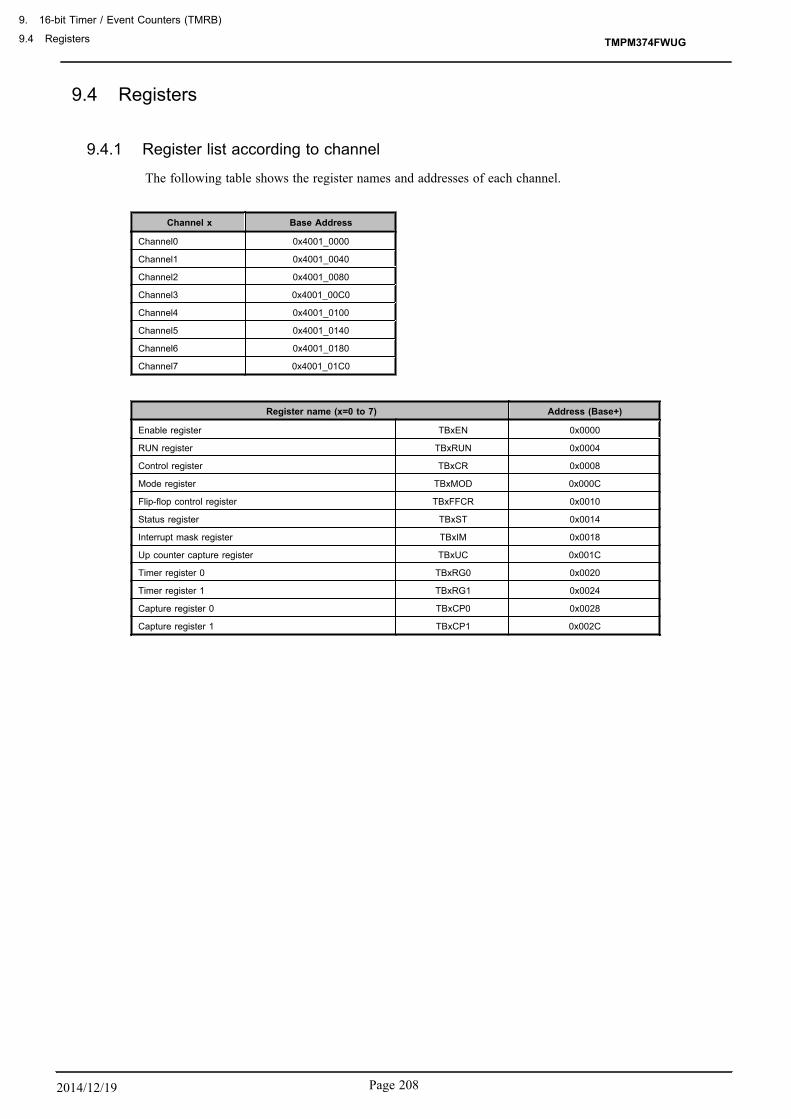
9.4 Registers
9.4.1 Register list according to channel
The following table shows the register names and addresses of each channel.
Channel x Base Address
Channel0 0x4001_0000
Channel1 0x4001_0040
Channel2 0x4001_0080
Channel3 0x4001_00C0
Channel4 0x4001_0100
Channel5 0x4001_0140
Channel6 0x4001_0180
Channel7 0x4001_01C0
Register name (x=0 to 7) Address (Base+)
Enable register TBxEN 0x0000
RUN register TBxRUN 0x0004
Control register TBxCR 0x0008
Mode register TBxMOD 0x000C
Flip-flop control register TBxFFCR 0x0010
Status register TBxST 0x0014
Interrupt mask register TBxIM 0x0018
Up counter capture register TBxUC 0x001C
Timer register 0 TBxRG0 0x0020
Timer register 1 TBxRG1 0x0024
Capture register 0 TBxCP0 0x0028
Capture register 1 TBxCP1 0x002C
TMPM374FWUG
9. 16-bit Timer / Event Counters (TMRB)
9.4 Registers
Page 2082014/12/19

9.4.2 TBxEN(Enable register)
31 30 29 28 27 26 25 24
bit symbol - - - - - - - -
After reset 0 0 0 0 0 0 0 0
23 22 21 20 19 18 17 16
bit symbol - - - - - - - -
After reset 0 0 0 0 0 0 0 0
15 14 13 12 11 10 9 8
bit symbol - - - - - - - -
After reset 0 0 0 0 0 0 0 0
7 6 5 4 3 2 1 0
bit symbol TBEN TBHALT - - - - - -
After reset 0 0 0 0 0 0 0 0
Bit Bit Symbol Type Function
31-8 − R Read as "0".
7 TBEN R/W TMRBx operation0: Disable1: Enable Specifies the TMRB operation. When the operation is disabled, no clock is supplied to the other registersin the TMRB module. This can reduce power consumption. (This disables reading from and writing to the oth-er registers except TBxEN register.)To use the TMRB, enable the TMRB operation (set to "1") before programming each register in the TMRBmodule. If the TMRB operation is executed and then disabled, the settings will be maintained in each register.
6 TBHALT R/W Clock operation during debug HALT.0: Run1: Stop
5-0 − R Read as "0".
TMPM374FWUG
Page 209 2014/12/19
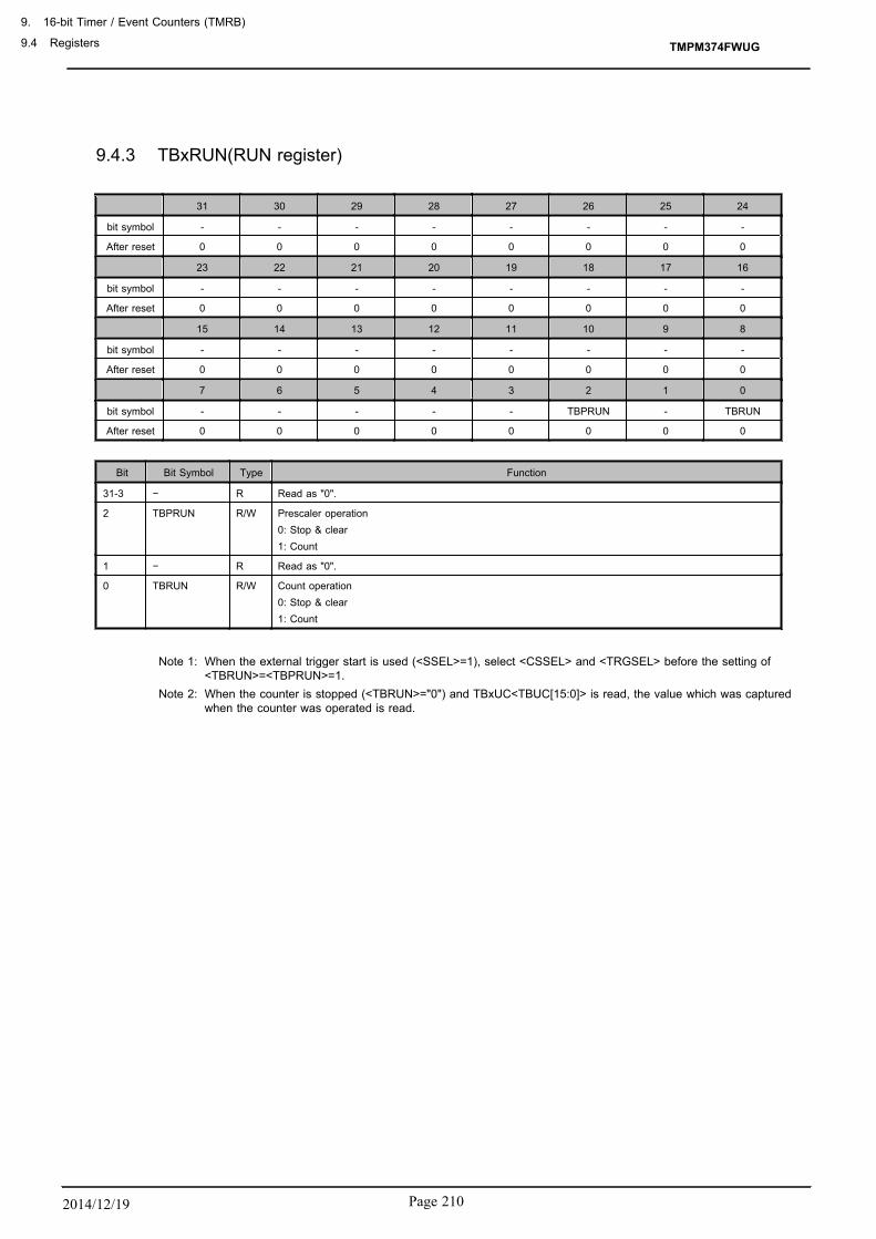
9.4.3 TBxRUN(RUN register)
31 30 29 28 27 26 25 24
bit symbol - - - - - - - -
After reset 0 0 0 0 0 0 0 0
23 22 21 20 19 18 17 16
bit symbol - - - - - - - -
After reset 0 0 0 0 0 0 0 0
15 14 13 12 11 10 9 8
bit symbol - - - - - - - -
After reset 0 0 0 0 0 0 0 0
7 6 5 4 3 2 1 0
bit symbol - - - - - TBPRUN - TBRUN
After reset 0 0 0 0 0 0 0 0
Bit Bit Symbol Type Function
31-3 − R Read as "0".
2 TBPRUN R/W Prescaler operation0: Stop & clear1: Count
1 − R Read as "0".
0 TBRUN R/W Count operation0: Stop & clear1: Count
Note 1: When the external trigger start is used (<SSEL>=1), select <CSSEL> and <TRGSEL> before the setting of<TBRUN>=<TBPRUN>=1.
Note 2: When the counter is stopped (<TBRUN>="0") and TBxUC<TBUC[15:0]> is read, the value which was capturedwhen the counter was operated is read.
TMPM374FWUG
9. 16-bit Timer / Event Counters (TMRB)
9.4 Registers
Page 2102014/12/19

9.4.4 TBxCR(Control register)
31 30 29 28 27 26 25 24
bit symbol - - - - - - - -
After reset 0 0 0 0 0 0 0 0
23 22 21 20 19 18 17 16
bit symbol - - - - - - - -
After reset 0 0 0 0 0 0 0 0
15 14 13 12 11 10 9 8
bit symbol - - - - - - - -
After reset 0 0 0 0 0 0 0 0
7 6 5 4 3 2 1 0
bit symbol TBWBF - - - I2TB - TRGSEL CSSEL
After reset 0 0 0 0 0 0 0 0
Bit Bit Symbol Type Function
31-8 − R Read as "0".
7 TBWBF R/W Double buffer0: Disable1: Enable
6-5 − R/W Write as "0".
4 − R Read as "0".
3 I2TB R/W Operation at IDLE mode0: Stop1: Operation
2 − R Read as "0".
1 TRGSEL R/W External Trigger select0: Rising edge1: Falling edge
0 CSSEL R/W Counter Start select0: Software start1: External trigger
Note 1: Do not modify TBxCR during operating TMRB.Note 2: When the external trigger start is used (<CSSEL>=1), select <CSSEL> and <TRGSEL> before the set-
ting of <TBRUN>=<TBPRUN>=1.
TMPM374FWUG
Page 211 2014/12/19

9.4.5 TBxMOD(Mode register)
31 30 29 28 27 26 25 24
bit symbol - - - - - - - -
After reset 0 0 0 0 0 0 0 0
23 22 21 20 19 18 17 16
bit symbol - - - - - - - -
After reset 0 0 0 0 0 0 0 0
15 14 13 12 11 10 9 8
bit symbol - - - - - - - -
After reset 0 0 0 0 0 0 0 0
7 6 5 4 3 2 1 0
bit symbol - TBRSWR TBCP TBCPM TBCLE TBCLK
After reset 0 0 1 0 0 0 0 0
Bit Bit Symbol Type Function
31-7 − R Read as "0".
6 TBRSWR R/W Writes to timer registers 0 and 1 (when double buffering is enabled)0: The data transfer to the timer register 0 and 1 is done by corresponding to the up-counter (UC) regard-less of the rewriting of the buffer register 0 and 1.1: To transfer the buffer registers data to the timer registers, the writing of the timer register 0 and 1 togeth-er are needed.
5 TBCP
W
Capture control by software0: Capture by software1: Don’t care When "0" is written, the capture register 0 (TBxCP0) takes count value.Read as "1".
4-3 TBCPM[1:0] R/W Capture timing00: Disable Capture timing01: TBxIN↑Takes count values into capture register 0 (TBxCP0) upon rising of TBxIN pin input.10: TBxIN↑ TBxIN↓Takes count values into capture register 0 (TBxCP0) upon rising of TBxIN pin input.Takes count values into capture register 1 (TBxCP1) upon falling of TBxIN pin input.11: Disable Capture timing
2 TBCLE R/W Up-counter control0: Disables clearing of the up-counter1: Enables clearing of the up-counter. Clears and controls the up-counter.When "0" is written, it disables clearing of the up-counter. When "1" is written, it clears up counter whenthere is a match with Timer Regsiter1 (TBxRG1).
1-0 TBCLK[1:0] R/W Selects the TMRBx source clock.00: TBxIN pin input01: φT110: φT411: φT16
Note:Do not change TBxMOD register while the timer is operating.
TMPM374FWUG
9. 16-bit Timer / Event Counters (TMRB)
9.4 Registers
Page 2122014/12/19
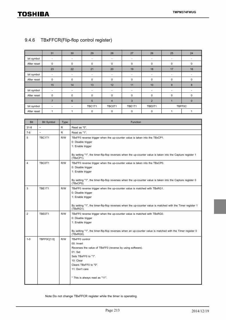
9.4.6 TBxFFCR(Flip-flop control register)
31 30 29 28 27 26 25 24
bit symbol - - - - - - - -
After reset 0 0 0 0 0 0 0 0
23 22 21 20 19 18 17 16
bit symbol - - - - - - - -
After reset 0 0 0 0 0 0 0 0
15 14 13 12 11 10 9 8
bit symbol - - - - - - - -
After reset 0 0 0 0 0 0 0 0
7 6 5 4 3 2 1 0
bit symbol - - TBC1T1 TBC0T1 TBE1T1 TBE0T1 TBFF0C
After reset 1 1 0 0 0 0 1 1
Bit Bit Symbol Type Function
31-8 − R Read as "0".
7-6 − R Read as "1".
5 TBC1T1 R/W TBxFF0 reverse trigger when the up-counter value is taken into the TBxCP1.0: Disable trigger1: Enable trigger By setting "1", the timer-flip-flop reverses when the up-counter value is taken into the Capture register 1(TBxCP1).
4 TBC0T1 R/W TBxFF0 reverse trigger when the up-counter value is taken into the TBxCP0.0: Disable trigger1: Enable trigger By setting "1", the timer-flip-flop reverses when the up-counter value is taken into the Capture register 0(TBxCP0).
3 TBE1T1 R/W TBxFF0 reverse trigger when the up-counter value is matched with TBxRG1.0: Disable trigger1: Enable trigger By setting "1", the timer-flip-flop reverses when the up-counter value is matched with the Timer register 1(TBxRG1).
2 TBE0T1 R/W TBxFF0 reverse trigger when the up-counter value is matched with TBxRG0.0: Disable trigger1: Enable trigger By setting "1", the timer-flip-flop reverses when an up-counter value is matched with the Timer register 0(TBxRG0).
1-0 TBFF0C[1:0] R/W TBxFF0 control00: InvertReverses the value of TBxFF0 (reverse by using software).01: SetSets TBxFF0 to "1".10: ClearClears TBxFF0 to "0".11: Don't care * This is always read as "11".
Note:Do not change TBxFFCR register while the timer is operating.
TMPM374FWUG
Page 213 2014/12/19

9.4.7 TBxST(Status register)
31 30 29 28 27 26 25 24
bit symbol - - - - - - - -
After reset 0 0 0 0 0 0 0 0
23 22 21 20 19 18 17 16
bit symbol - - - - - - - -
After reset 0 0 0 0 0 0 0 0
15 14 13 12 11 10 9 8
bit symbol - - - - - - - -
After reset 0 0 0 0 0 0 0 0
7 6 5 4 3 2 1 0
bit symbol - - - - - INTTBOF INTTB1 INTTB0
After reset 0 0 0 0 0 0 0 0
Bit Bit Symbol Type Function
31-3 − R Read as "0".
2 INTTBOF R Overflow flag0: No overflow occurs1: Overflow occursWhen an up-counter is overflow, "1" is set.
1 INTTB1 R Match flag (TBxRG1)0: No match is detected1: Detects a match with TBxRG1When a match with the timer register 1 (TBxRG1) is detected,"1" is set.
0 INTTB0 R Match flag (TBxRG0)0: No match is detected1: Detects a match with TBxRG0When a match with the timer register 0 (TBxRG0) is detected, "1" is set.
Note 1: The factors only which is not masked by TBxIM output interrupt request to the CPU.Even if the mask setting isdone, the flag is set.
Note 2: The flag is cleared by reading the TBxST register.To clear the flag, TBxST register should be read.
TMPM374FWUG
9. 16-bit Timer / Event Counters (TMRB)
9.4 Registers
Page 2142014/12/19
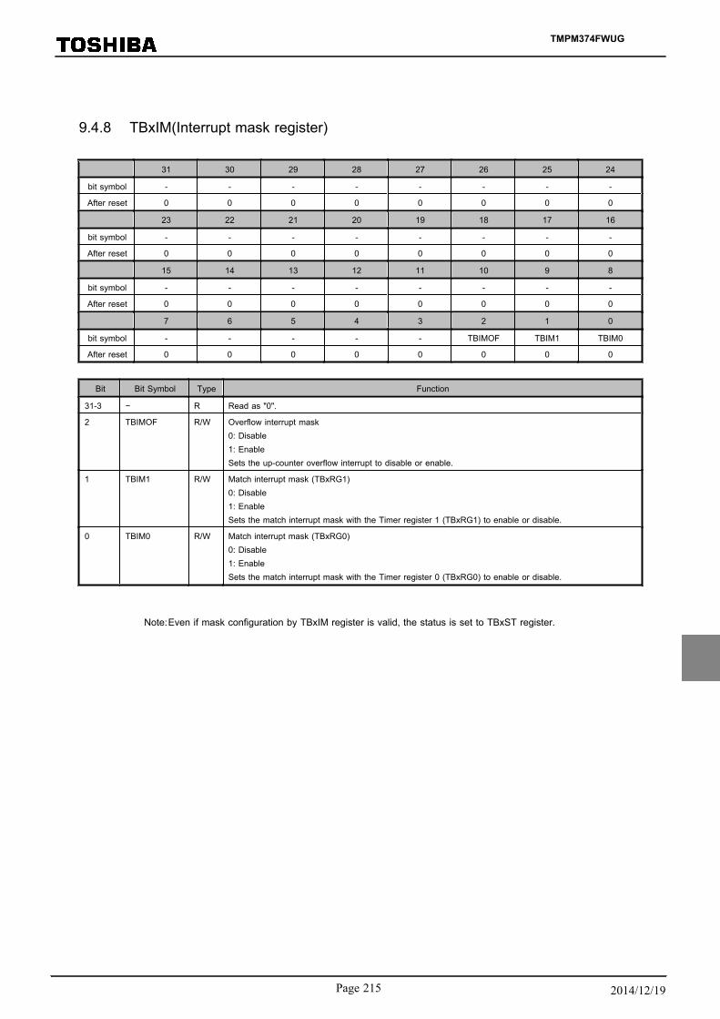
9.4.8 TBxIM(Interrupt mask register)
31 30 29 28 27 26 25 24
bit symbol - - - - - - - -
After reset 0 0 0 0 0 0 0 0
23 22 21 20 19 18 17 16
bit symbol - - - - - - - -
After reset 0 0 0 0 0 0 0 0
15 14 13 12 11 10 9 8
bit symbol - - - - - - - -
After reset 0 0 0 0 0 0 0 0
7 6 5 4 3 2 1 0
bit symbol - - - - - TBIMOF TBIM1 TBIM0
After reset 0 0 0 0 0 0 0 0
Bit Bit Symbol Type Function
31-3 − R Read as "0".
2 TBIMOF R/W Overflow interrupt mask0: Disable1: EnableSets the up-counter overflow interrupt to disable or enable.
1 TBIM1 R/W Match interrupt mask (TBxRG1)0: Disable1: EnableSets the match interrupt mask with the Timer register 1 (TBxRG1) to enable or disable.
0 TBIM0 R/W Match interrupt mask (TBxRG0)0: Disable1: EnableSets the match interrupt mask with the Timer register 0 (TBxRG0) to enable or disable.
Note:Even if mask configuration by TBxIM register is valid, the status is set to TBxST register.
TMPM374FWUG
Page 215 2014/12/19
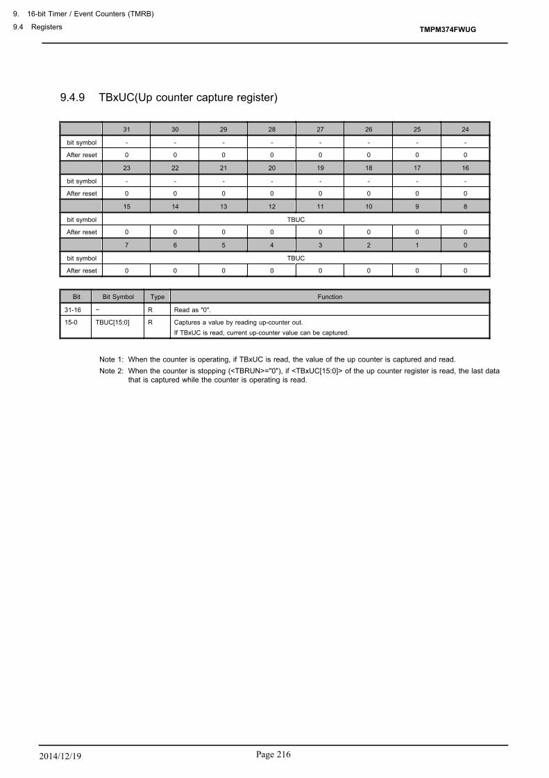
9.4.9 TBxUC(Up counter capture register)
31 30 29 28 27 26 25 24
bit symbol - - - - - - - -
After reset 0 0 0 0 0 0 0 0
23 22 21 20 19 18 17 16
bit symbol - - - - - - - -
After reset 0 0 0 0 0 0 0 0
15 14 13 12 11 10 9 8
bit symbol TBUC
After reset 0 0 0 0 0 0 0 0
7 6 5 4 3 2 1 0
bit symbol TBUC
After reset 0 0 0 0 0 0 0 0
Bit Bit Symbol Type Function
31-16 − R Read as "0".
15-0 TBUC[15:0] R Captures a value by reading up-counter out.If TBxUC is read, current up-counter value can be captured.
Note 1: When the counter is operating, if TBxUC is read, the value of the up counter is captured and read.Note 2: When the counter is stopping (<TBRUN>="0"), if <TBxUC[15:0]> of the up counter register is read, the last data
that is captured while the counter is operating is read.
TMPM374FWUG
9. 16-bit Timer / Event Counters (TMRB)
9.4 Registers
Page 2162014/12/19
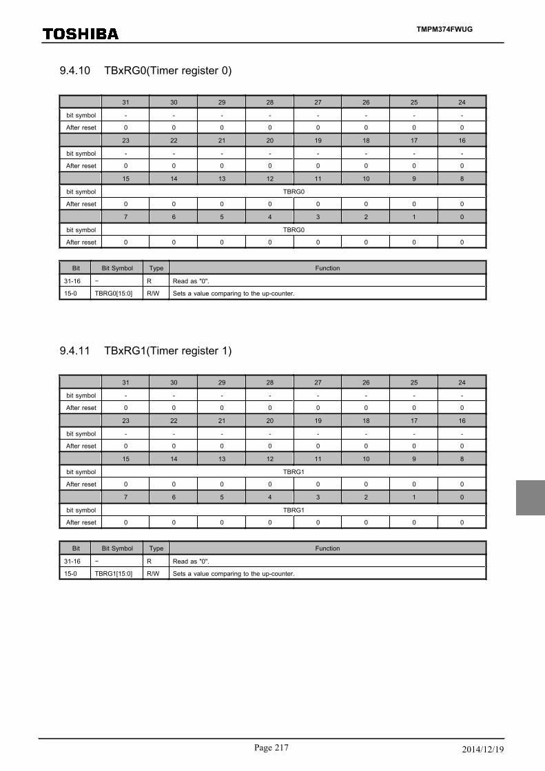
9.4.10 TBxRG0(Timer register 0)
31 30 29 28 27 26 25 24
bit symbol - - - - - - - -
After reset 0 0 0 0 0 0 0 0
23 22 21 20 19 18 17 16
bit symbol - - - - - - - -
After reset 0 0 0 0 0 0 0 0
15 14 13 12 11 10 9 8
bit symbol TBRG0
After reset 0 0 0 0 0 0 0 0
7 6 5 4 3 2 1 0
bit symbol TBRG0
After reset 0 0 0 0 0 0 0 0
Bit Bit Symbol Type Function
31-16 − R Read as "0".
15-0 TBRG0[15:0] R/W Sets a value comparing to the up-counter.
9.4.11 TBxRG1(Timer register 1)
31 30 29 28 27 26 25 24
bit symbol - - - - - - - -
After reset 0 0 0 0 0 0 0 0
23 22 21 20 19 18 17 16
bit symbol - - - - - - - -
After reset 0 0 0 0 0 0 0 0
15 14 13 12 11 10 9 8
bit symbol TBRG1
After reset 0 0 0 0 0 0 0 0
7 6 5 4 3 2 1 0
bit symbol TBRG1
After reset 0 0 0 0 0 0 0 0
Bit Bit Symbol Type Function
31-16 − R Read as "0".
15-0 TBRG1[15:0] R/W Sets a value comparing to the up-counter.
TMPM374FWUG
Page 217 2014/12/19

9.4.12 TBxCP0(Capture register 0)
31 30 29 28 27 26 25 24
bit symbol - - - - - - - -
After reset 0 0 0 0 0 0 0 0
23 22 21 20 19 18 17 16
bit symbol - - - - - - - -
After reset 0 0 0 0 0 0 0 0
15 14 13 12 11 10 9 8
bit symbol TBCP0
After reset 0 0 0 0 0 0 0 0
7 6 5 4 3 2 1 0
bit symbol TBCP0
After reset 0 0 0 0 0 0 0 0
Bit Bit Symbol Type Function
31-16 − R Read as "0".
15-0 TBCP0[15:0] R A value captured from the up-counter is read.
9.4.13 TBxCP1(Capture register 1)
31 30 29 28 27 26 25 24
bit symbol - - - - - - - -
After reset 0 0 0 0 0 0 0 0
23 22 21 20 19 18 17 16
bit symbol - - - - - - - -
After reset 0 0 0 0 0 0 0 0
15 14 13 12 11 10 9 8
bit symbol TBCP1
After reset 0 0 0 0 0 0 0 0
7 6 5 4 3 2 1 0
bit symbol TBCP1
After reset 0 0 0 0 0 0 0 0
Bit Bit Symbol Type Function
31-16 − R Read as "0".
15-0 TBCP1[15:0] R A value captured from the up-counter is read.
TMPM374FWUG
9. 16-bit Timer / Event Counters (TMRB)
9.4 Registers
Page 2182014/12/19
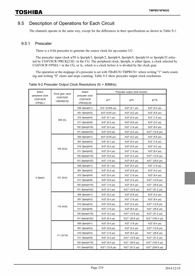
9.5 Description of Operations for Each CircuitThe channels operate in the same way, except for the differences in their specifications as shown in Table 9-1.
9.5.1 Prescaler
There is a 4-bit prescaler to generate the source clock for up-counter UC.
The prescaler input clock φT0 is fperiph/1, fperiph/2, fperiph/4, fperiph/8, fperiph/16 or fperiph/32 selec-ted by CGSYSCR<PRCK[2:0]> in the CG. The peripheral clock, fperiph, is either fgear, a clock selected byCGSYSCR<FPSEL> in the CG, or fc, which is a clock before it is divided by the clock gear.
The operation or the stoppage of a prescaler is set with TBxRUN<TBPRUN> where writing "1" starts count-ing and writing "0" clears and stops counting. Table 9-2 show prescaler output clock resolutions.
Table 9-2 Prescaler Output Clock Resolutions (fc = 80MHz)
Selectperipheral clock
CGSYSCR<FPSEL>
Clock gear valueCGSYSCR
<GEAR[2:0]>
Selectprescaler clock
CGSYSCR<PRCK[2:0]>
Prescaler output clock function
φT1 φT4 φT16
0 (fgear)
000 (fc)
000 (fperiph/1) fc/21 (0.025 μs) fc/23 (0.1 μs) fc/25 (0.4 μs)
001 (fperiph/2) fc/22 (0.05 μs) fc/24 (0.2 μs) fc/26 (0.8 μs)
010 (fperiph/4) fc/23 (0.1 μs) fc/25 (0.4 μs) fc/27 (1.6 μs)
011 (fperiph/8) fc/24 (0.2 μs) fc/26 (0.8 μs) fc/28 (3.2 μs)
100 (fperiph/16) fc/25 (0.4 μs) fc/27 (1.6 μs) fc/29 (6.4 μs)
101 (fperiph/32) fc/26 (0.8 μs) fc/28 (3.2 μs) fc/210 (12.8 μs)
100 (fc/2)
000 (fperiph/1) fc/22 (0.05 μs) fc/24 (0.2 μs) fc/26 (0.8 μs)
001 (fperiph/2) fc/23 (0.1 μs) fc/25 (0.4 μs) fc/27 (1.6 μs)
010 (fperiph/4) fc/24 (0.2 μs) fc/26 (0.8 μs) fc/28 (3.2 μs)
011 (fperiph/8) fc/25 (0.4 μs) fc/27 (1.6 μs) fc/29 (6.4 μs)
100 (fperiph/16) fc/26 (0.8 μs) fc/28 (3.2 μs) fc/210 (12.8 μs)
101 (fperiph/32) fc/27 (1.6 μs) fc/29 (6.4 μs) fc/211 (25.6 μs)
101 (fc/4)
000 (fperiph/1) fc/23 (0.1 μs) fc/25 (0.4 μs) fc/27 (1.6 μs)
001 (fperiph/2) fc/24 (0.2 μs) fc/26 (0.8 μs) fc/28 (3.2 μs)
010 (fperiph/4) fc/25 (0.4 μs) fc/27 (1.6 μs) fc/29 (6.4 μs)
011 (fperiph/8) fc/26 (0.8 μs) fc/28 (3.2 μs) fc/210 (12.8 μs)
100 (fperiph/16) fc/27 (1.6 μs) fc/29 (6.4 μs) fc/211 (25.6 μs)
101 (fperiph/32) fc/28 (3.2 μs) fc/210 (12.8 μs) fc/212 (51.2 μs)
110 (fc/8)
000 (fperiph/1) fc/24 (0.2 μs) fc/26 (0.8 μs) fc/28 (3.2 μs)
001 (fperiph/2) fc/25 (0.4 μs) fc/27 (1.6 μs) fc/29 (6.4 μs)
010 (fperiph/4) fc/26 (0.8 μs) fc/28 (3.2 μs) fc/210 (12.8 μs)
011 (fperiph/8) fc/27 (1.6 μs) fc/29 (6.4 μs) fc/211 (25.6 μs)
100 (fperiph/16) fc/28 (3.2 μs) fc/210 (12.8 μs) fc/212 (51.2 μs)
101 (fperiph/32) fc/29 (6.4 μs) fc/211 (25.6 μs) fc/213 (102.4 μs)
111 (fc/16)
000 (fperiph/1) fc/25 (0.4 μs) fc/27 (1.6 μs) fc/29 (6.4 μs)
001 (fperiph/2) fc/26 (0.8 μs) fc/28 (3.2 μs) fc/210 (12.8 μs)
010 (fperiph/4) fc/27 (1.6 μs) fc/29 (6.4 μs) fc/211 (25.6 μs)
011 (fperiph/8) fc/28 (3.2 μs) fc/210 (12.8 μs) fc/212 (51.2 μs)
100 (fperiph/16) fc/29 (6.4 μs) fc/211 (25.6 μs) fc/213 (102.4 μs)
101 (fperiph/32) fc/210 (12.8 μs) fc/212 (51.2 μs) fc/214 (204.8 μs)
TMPM374FWUG
Page 219 2014/12/19
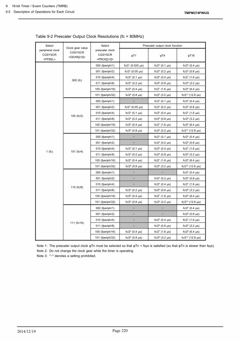
Table 9-2 Prescaler Output Clock Resolutions (fc = 80MHz)
Selectperipheral clock
CGSYSCR<FPSEL>
Clock gear valueCGSYSCR
<GEAR[2:0]>
Selectprescaler clock
CGSYSCR<PRCK[2:0]>
Prescaler output clock function
φT1 φT4 φT16
1 (fc)
000 (fc)
000 (fperiph/1) fc/21 (0.025 μs) fc/23 (0.1 μs) fc/25 (0.4 μs)
001 (fperiph/2) fc/22 (0.05 μs) fc/24 (0.2 μs) fc/26 (0.8 μs)
010 (fperiph/4) fc/23 (0.1 μs) fc/25 (0.4 μs) fc/27 (1.6 μs)
011 (fperiph/8) fc/24 (0.2 μs) fc/26 (0.8 μs) fc/28 (3.2 μs)
100 (fperiph/16) fc/25 (0.4 μs) fc/27 (1.6 μs) fc/29 (6.4 μs)
101 (fperiph/32) fc/26 (0.8 μs) fc/28 (3.2 μs) fc/210 (12.8 μs)
100 (fc/2)
000 (fperiph/1) − fc/23 (0.1 μs) fc/25 (0.4 μs)
001 (fperiph/2) fc/22 (0.05 μs) fc/24 (0.2 μs) fc/26 (0.8 μs)
010 (fperiph/4) fc/23 (0.1 μs) fc/25 (0.4 μs) fc/27 (1.6 μs)
011 (fperiph/8) fc/24 (0.2 μs) fc/26 (0.8 μs) fc/28 (3.2 μs)
100 (fperiph/16) fc/25 (0.4 μs) fc/27 (1.6 μs) fc/29 (6.4 μs)
101 (fperiph/32) fc/26 (0.8 μs) fc/28 (3.2 μs) fc/210 (12.8 μs)
101 (fc/4)
000 (fperiph/1) − fc/23 (0.1 μs) fc/25 (0.4 μs)
001 (fperiph/2) − fc/24 (0.2 μs) fc/26 (0.8 μs)
010 (fperiph/4) fc/23 (0.1 μs) fc/25 (0.4 μs) fc/27 (1.6 μs)
011 (fperiph/8) fc/24 (0.2 μs) fc/26 (0.8 μs) fc/28 (3.2 μs)
100 (fperiph/16) fc/25 (0.4 μs) fc/27 (1.6 μs) fc/29 (6.4 μs)
101 (fperiph/32) fc/26 (0.8 μs) fc/28 (3.2 μs) fc/210 (12.8 μs)
110 (fc/8)
000 (fperiph/1) − − fc/25 (0.4 μs)
001 (fperiph/2) − fc/24 (0.2 μs) fc/26 (0.8 μs)
010 (fperiph/4) − fc/25 (0.4 μs) fc/27 (1.6 μs)
011 (fperiph/8) fc/24 (0.2 μs) fc/26 (0.8 μs) fc/28 (3.2 μs)
100 (fperiph/16) fc/25 (0.4 μs) fc/27 (1.6 μs) fc/29 (6.4 μs)
101 (fperiph/32) fc/26 (0.8 μs) fc/28 (3.2 μs) fc/210 (12.8 μs)
111 (fc/16)
000 (fperiph/1) − − fc/25 (0.4 μs)
001 (fperiph/2) − − fc/26 (0.8 μs)
010 (fperiph/4) − fc/25 (0.4 μs) fc/27 (1.6 μs)
011 (fperiph/8) − fc/26 (0.8 μs) fc/28 (3.2 μs)
100 (fperiph/16) fc/25 (0.4 μs) fc/27 (1.6 μs) fc/29 (6.4 μs)
101 (fperiph/32) fc/26 (0.8 μs) fc/28 (3.2 μs) fc/210 (12.8 μs)
Note 1: The prescaler output clock φTn must be selected so that φTn < fsys is satisfied (so that φTn is slower than fsys).Note 2: Do not change the clock gear while the timer is operating.Note 3: "−" denotes a setting prohibited.
TMPM374FWUG
9. 16-bit Timer / Event Counters (TMRB)
9.5 Description of Operations for Each Circuit
Page 2202014/12/19
9.5.2 Up-counter (UC)
UC is a 16-bit binary counter.
・ Source clock
UC source clock, specified by TBxMOD<TBCLK[1:0]>, can be selected from either three typesφT1, φT4, φT16 of prescaler output clock or the external clock of the TBxIN pin.
・ Count start / stop
Counter operation is specified by TBxRUN<TBRUN>. UC starts counting if <TBRUN> = "1",and stops counting and clears counter value if <TBRUN> = "0".
・ Timing to clear UC
1. When a match is detected
By setting TBxMOD<TBCLE> = "1", UC is cleared if when the comparator detects amatch between counter value and the value set in TBxRG1. UC operates as a free-running coun-ter if TBxMOD<TBCLE> = "0".
2. When UC stops
UC stops counting and clears counter value if TBxRUN<TBRUN> = "0".
・ UC overflow
If UC overflow occurs, the INTTBx0 overflow interrupt is generated.
9.5.3 Timer registers (TBxRG0, TBxRG1)
TBxRG0 and TBxRG1 are registers for setting values to compare with up-counter values and two registersare built into each channel. If the comparator detects a match between a value set in this timer register andthat in a UC up-counter, it outputs the match detection signal.
TBxRG0 and TBxRG1 are consisted of the double-buffered configuration which are paired with register buf-fers. The double buffering is disabled in the initial state.
Controlling double buffering disable or enable is specified by TBxCR<TBWBF> bit. If <TBWBF> = "0",the double buffering becomes disable. If <TBWBF> = "1", it becomes enable. When the double buffering is en-abled, a data transfer from the register buffer to the timer register (TBxRG0/1) is done in the case that UC ismatched with TBxRG1. When the counter is stopped even if double buffering is enabled, the double buffer-ing operates as a single buffer, and an immediate data can be written to the TBxRG0 and TBxRG1.
9.5.4 Capture
This is a circuit that controls the timing of latching values from the UC up-counter into the TBxCP0 andTBxCP1 capture registers. The timing with which to latch data is specified by TBxMOD<TBCPM[1:0]>.
Software can also be used to import values from the UC up-counter into the capture register; specifically,UC values are taken into the TBxCP0 capture register each time "0" is written to TBxMOD<TBCP>.
9.5.5 Capture register (TBxCP0, TBxCP1)
This register captures an up-counter (UC) value.
TMPM374FWUG
Page 221 2014/12/19
To read data from the capture register, use a 16-bit data transfer instruction or read in the order of low-or-der bits followed by high-order bits.
9.5.6 Up counter capture register (TBxUC)
Other than the capturing functions shown above, the current count value of the UC can be captured by read-ing the TBxUC registers.
9.5.7 Comparators (CP0, CP1)
This register compares with the up-counter (UC) and the value setting of the Timer Register (TBxRG0and TBxRG1) to detect whether there is a match or not. If a match is detected, INTTBx0 and INTTBx1 are gen-erated.
9.5.8 Timer Flip-flop (TBxFF0)
The timer flip-flop (TBxFF0) is reversed by a match signal from the comparator and a latch signal to the cap-ture registers. It can be enabled or disabled to reverse by setting the TBxFFCR<TBC1T1, TBC0T1,TBE1T1, TBE0T1>.
The value of TBxFF0 becomes undefined after a reset. The flip-flop can be reversed by writing "00" toTBxFFCR<TBFF0C[1:0]>. It can be set to "1" by writing "01," and can be cleared to "0" by writing "10."
The value of TBxFF0 can be output to the Timer output pin (TBxOUT). If the timer output is performed,the corresponding port settings must be programmed beforehand.
9.5.9 Capture interrupt (INTCAPx0, INTCAPx1)
Interrupts INTCAPx0 and INTCAPx1 can be generated at the timing of latching values from the UC up-coun-ter into the TBxCP0 and TBxCP1 capture registers. The interrupt timing is specified by the CPU.
TMPM374FWUG
9. 16-bit Timer / Event Counters (TMRB)
9.5 Description of Operations for Each Circuit
Page 2222014/12/19

9.6 Description of Operations for Each Mode
9.6.1 16-bit Interval Timer Mode
In the case of generating constant period interrupt, set the interval time to the Timer register (TBxRG0) togenerate the INTTBx0 interrupt. Same as TBxRG0, INTTBx1 interrupt is generated by setting different inter-val time value to TBxRG1 timer resister.
7 6 5 4 3 2 1 0
TBxEN ← 1 X X X X X X X Enables TMRBx operation.
TBxRUN ← X X X X X 0 X 0 Stops count operation.
Interrupt Set-EnableRegister
← * * * * * * * * Permits INTTBx1 interrupt by setting corresponding bit to "1".
TBxFFCR ← X X 0 0 0 0 1 1 Disable to TBxFF0 reverse trigger.
TBxMOD ← X 0 1 0 0 1 * * Changes to prescaler output clock as input clock. Specifiescapture function to disable. (** = 01, 10, 11)
TBxRG1 ← * * * * * * * * Specifies a time interval. (16 bits)
← * * * * * * * *
TBxRUN ← * * * * * 1 X 1 Starts TMRBx.
Note:X; Don’t care −; No change
9.6.2 16-bit Event Counter Mode
It is possible to make it the event counter by using an input clock as an external clock (TBxIN pin input).
The up-counter counts up on the rising edge of TBxIN pin input. It is possible to read the count value by cap-turing value using software and reading the captured value.
7 6 5 4 3 2 1 0
TBxEN ← 1 X X X X X X X Enables TMRBx operation.
TBxRUN ← X X X X X 0 X 0 Stops count operation.
Set PORT registers. Allocates corresponding port to TBxIN.
TBxFFCR ← X X 0 0 0 0 1 1 Disable to TBxFF0 reverse trigger.
TBxMOD ← X 0 1 0 0 0 0 0 Changes to TBxIN as an input clock.
TBxRUN ← * * * * * 1 X 1 Starts TMRBx.
TBxMOD ← X 0 0 0 0 0 0 0 Software capture is done.
Note:X; Don’t care −; No change
TMPM374FWUG
Page 223 2014/12/19

9.6.3 16-bit PPG (Programmable Pulse Generation) Output Mode
Square waves with any frequency and any duty (programmable square waves) can be output. The outputpulse can be either low-active or high-active.
Programmable square waves can be output from the TBxOUT pin by triggering the timer flip-flop(TBxFF) to reverse when the set value of the up-counter (UC) matches the set values of the timer registers(TBxRG0 and TBxRG1). Note that the set values of TBxRG0 and TBxRG1 must satisfy the following require-ment:
Set value of TBxRG0 < Set value of TBxRG1
TBxOUT pin
Match with TBxRG0(INTTBx0 interrupt)
Match with TBxRG1(INTTBx1 interrupt)
Figure 9-2 Example of Output of Programmable Pulse Generation (PPG)
In this mode, by enabling the double buffering of TBxRG0, the value of register buffer 0 is shifted intoTBxRG0 when the set value of the up-counter matches the set value of TBxRG1. This facilitates handling ofsmall duties.
Q2Q1
Match with TBxRG1
TBxRG0(compare value)
Q3Q2Register buffer
Trigger to shift to TBxRG1
Write TBxRG0
Up-counter= Q1 Up-counter= Q2Match with TBxRG0
Q5Q4TBxRG1(compare value)
Q6Q5Register buffer
Write TBxRG1
Figure 9-3 Register Buffer Operation
TMPM374FWUG
9. 16-bit Timer / Event Counters (TMRB)
9.6 Description of Operations for Each Mode
Page 2242014/12/19

The block diagram of this mode is shown below.
Selector
Selector
Internal data bus
TBxCR<TBWBF>
WriteTBxRG0
TBxOUT (PPG output)
TBxRUN<TBRUN>
Match
TBxINT1T4
T16
TBxRG0
Clear16-bit up-counterUC
TBxRG1
F/F(TBxFF0)
Selector
WriteTBxRG1
TBxCR<TBWBF>
16-bit comparator 16-bit comparator
Register buffer 0 Register buffer 1
Figure 9-4 Block Diagram of 16-bit PPG Mode
Each register in the 16-bit PPG output mode must be programmed as listed below.
7 6 5 4 3 2 1 0
TBxEN ← 1 X X X X X X X Enables TMRBx operation.
TBxRUN ← X X X X X 0 X 0 Stops count operation.
TBxCR ← 0 0 − X − X 0 0 Disables double buffering.
TBxRG0 ← * * * * * * * * Specifies a duty. (16 bits)
← * * * * * * * *
TBxRG1 ← * * * * * * * * Specifies a cycle. (16 bits)
← * * * * * * * *
TBxCR ← 1 0 − X − X 0 0 Enables the TBxRG0 double buffering.
(Changes the duty/cycle when the INTTBx0 interrupt is gener-ated)
TBxFFCR ← X X 0 0 1 1 1 0
Specifies to trigger TBxFF0 to reverse when a match withTBxRG0 or TBxRG1 is detected, and sets the initial value ofTBxFF0 to "0".
TBxMOD ← X 0 1 0 0 1 * * Designates the prescaler output clock as the input clock, anddisables the capture function. UC is cleared to match TBxRG1.
(** = 01, 10, 11)
Set PORT registers. Allocates corresponding port to TBxOUT.
TBxRUN ← * * * * * 1 X 1 Starts TMRBx.
Note:X; Don’t care−; No change
TMPM374FWUG
Page 225 2014/12/19

9.6.4 External trigger Programmable Pulse Generation Output Mode (PPG)
Using an external count start trigger enables one-shot pulse generation with a short delay.
The figure below shows the example of an one-shot pulse output (with delay). This one-shot pulse is gener-ated from the external trigger start.
The 16-bit up-counter (UC) is programmed to count up on the rising edge of the TBxIN pin (TBxCR[1:0]= "01"). The TBxRG0 is loaded with the pulse delay (d), and the TBxRG1 is loaded with the sum of theTBxRG0 value (d) and the pulse width (p). The above settings must be done while the 16-bit up-counter is stop-ped (TBxRUN<TBRUN> = 0).
To enable the trigger for timer flip-flop, sets TBxFFCR<TBE1T1, TBE0T1> to "11". With this setting, thetimer flip-flop reverses when 16-bit up-counter (UC) corresponds to TBxRG0 or TBxRG1.
Sets TBxRUN<TBRUN> to "1" to enable the count-up by an external trigger.
After the generation of one-shot pulse by the external trigger, to disable reverse of the timer flip-flop or tostop 16bit counter by TBxRUN<TBRUN> setting.
Symbols (d) and (p) used in the text correspond to symbols d and p in Figure 9-5.
Counter Clock(Internal Clock)
Timer output TBxOUT pin
TBxIN Input PIn(External Trigger Pulse)
Match with TBxRG0
Match with TBxRG1
0
(p)
d d + p
Reverse
The counter starts at the rising edge of external trigger.
INTTBx1 generation
Pulse width
(d)
Delay time
INTTBx0generation
Reverse
Figure 9-5 One-shot pulse generation using an external count start trigger (with a delay)
TMPM374FWUG
9. 16-bit Timer / Event Counters (TMRB)
9.6 Description of Operations for Each Mode
Page 2262014/12/19

9.7 Applications using the Capture FunctionThe capture function can be used to develop many applications, including those described below:
1. One-shot pulse output triggered by an external pulse
2. Pulse width measurement
9.7.1 One-shot pulse output triggered by an external pulse
One-shot pulse output triggered by an external pulse is carried out as follows:
The 16-bit up-counter is made to count up by putting it in a free-running state using the prescaler outputclock. An external pulse is input through the TBxIN pin. A trigger is generated at the rising of the externalpulse by using the capture function and the value of the up-counter is taken into the capture registers (TBxCP0).
The CPU must be programmed so that an interrupt INTCAPx0 is generated at the rising of an external trig-ger pulse. This interrupt is used to set the timer registers (TBxRG0) to the sum of the TBxCP0 value (c) andthe delay time (d), (c + d), and set the timer registers (TBxRG1) to the sum of the TBxRG0 values and thepulse width (p) of one-shot pulse, (c + d + p).[TBxRG1 change must be completed before the next match.]
In addition, the timer flip-flop control registers(TBxFFCR<TBE1T1, TBE0T1>) must be set to "11". This en-ables triggering the timer flip-flop (TBxFF0) to reverse when TBxUC matches TBxRG0 and TBxRG1. Thistrigger is disabled by the INTTBx0 / INTTBx1 interrupt after a one-shot pulse is output.
Symbols (c), (d) and (p) used in the text correspond to symbols c, d and p in Figure 9-6.
Count clock(Internal clock)
Timer output TBxOUT pin
TBxIN pin input(External trigger pulse)
Match with TBxRG0
Match with TBxRG1
c
(p)
c + d c + d + p
Enable reverse
Enable reverse
Put the counter in a free-running state.
Taking data into the capture register (TBxCP0).
INTTBx1 generation
Disable reversewhen data is takeninto TBxCP0.
Pulse width
(d)
Delay time
INTTBx0 generation
INTCAPx0 generation
Figure 9-6 One-shot Pulse Output (With Delay)
TMPM374FWUG
Page 227 2014/12/19
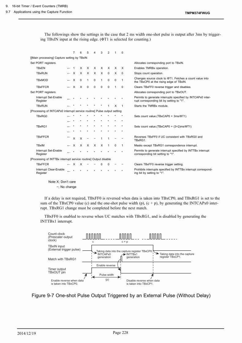
The followings show the settings in the case that 2 ms width one-shot pulse is output after 3ms by trigger-ing TBxIN input at the rising edge. (ΦT1 is selected for counting.)
7 6 5 4 3 2 1 0
[[Main processing] Capture setting by TBxIN
Set PORT registers. Allocates corresponding port to TBxIN.
TBxEN ← 1 X X X X X X X Enables TMRBx operation.
TBxRUN ← X X X X X 0 X 0 Stops count operation.
TBxMOD ← X 0 1 0 1 0 0 1 Changes source clock to ΦT1. Fetches a count value intothe TBxCP0 at the rising edge of TBxIN.
TBxFFCR ← X X 0 0 0 0 1 0 Clears TBxFF0 reverse trigger and disables.
Set PORT registers. Allocates corresponding port to TBxOUT.
Interrupt Set-EnableRegister ← * * * * * * * * Permits to generate interrupts specified by INTCAPx0 inter-
rupt corresponding bit by setting to "1".
TBxRUN ← * * * * * 1 X 1 Starts the TMRBx module.
[Processing of INTCAPx0 interrupt service routine] Pulse output setting
TBxRG0 ← * * * * * * * * Sets count value.(TBxCAP0 + 3ms/ΦT1)
← * * * * * * * *
TBxRG1 ← * * * * * * * * Sets count value.(TBxCAP0 + (3+2)ms/ΦT1)
← * * * * * * * *
TBxFFCR ← X X − − 1 1 − − Reverses TBxFF0 if UC consistent with TBxRG0 andTBxRG1.
TBxIM ← X X X X X 1 0 1 Masks except TBxRG1 correspondence interrupt.
Interrupt Set-EnableRegister ← * * * * * * * * Permits to generate interrupt specified by INTTBx interrupt
corresponding bit setting to "1".
[Processing of INTTBx interrupt service routine] Output disable
TBxFFCR ← X X − − 0 0 − − Clears TBxFF0 reverse trigger setting.
Interrupt Clear-EnableRegister ← * * * * * * * * Prohibits interrupts specified by INTTBx interrupt correspond-
ing bit by setting to "1".
Note:X; Don’t care−; No change
If a delay is not required, TBxFF0 is reversed when data is taken into TBxCP0, and TBxRG1 is set to thesum of the TBxCP0 value (c) and the one-shot pulse width (p), (c + p), by generating the INTCAPx0 inter-rupt. TBxRG1 change must be completed before the next match.
TBxFF0 is enabled to reverse when UC matches with TBxRG1, and is disabled by generating theINTTBx1 interrupt.
Count clock(Prescaler outputclock)
Timer outputTBxOUT pin
TBxIN input(External trigger pulse)
Match with TBxRG1
c
(p)
c + p
Enable reverse
INTTBx1generation
Enable reverse when datais taken into TBxCP0.
Taking data into the capture register TBxCP0.Taking data into the captureregister TBxCP1.
Disable reverse when datais taken into TBxCP1.
Pulse width
INTCAPx0generation
Figure 9-7 One-shot Pulse Output Triggered by an External Pulse (Without Delay)
TMPM374FWUG
9. 16-bit Timer / Event Counters (TMRB)
9.7 Applications using the Capture Function
Page 2282014/12/19
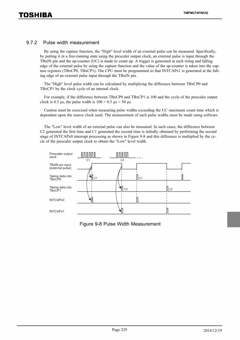
9.7.2 Pulse width measurement
By using the capture function, the "High" level width of an external pulse can be measured. Specifically,by putting it in a free-running state using the prescaler output clock, an external pulse is input through theTBxIN pin and the up-counter (UC) is made to count up. A trigger is generated at each rising and fallingedge of the external pulse by using the capture function and the value of the up-counter is taken into the cap-ture registers (TBxCP0, TBxCP1). The CPU must be programmed so that INTCAPx1 is generated at the fall-ing edge of an external pulse input through the TBxIN pin.
The "High" level pulse width can be calculated by multiplying the difference between TBxCP0 andTBxCP1 by the clock cycle of an internal clock.
For example, if the difference between TBxCP0 and TBxCP1 is 100 and the cycle of the prescaler outputclock is 0.5 μs, the pulse width is 100 × 0.5 μs = 50 μs.
Caution must be exercised when measuring pulse widths exceeding the UC maximum count time which isdependant upon the source clock used. The measurement of such pulse widths must be made using software.
The "Low" level width of an external pulse can also be measured. In such cases, the difference betweenC2 generated the first time and C1 generated the second time is initially obtained by performing the secondstage of INTCAPx0 interrupt processing as shown in Figure 9-8 and this difference is multiplied by the cy-cle of the prescaler output clock to obtain the "Low" level width.
Prescaler outputclock
Taking data intoTBxCP1
TBxIN pin input(external pulse)
Taking data intoTBxCP0
C1
C1 C1
C2
C2 C2
INTCAPx1
INTCAPx0
Figure 9-8 Pulse Width Measurement
TMPM374FWUG
Page 229 2014/12/19

TMPM374FWUG
9. 16-bit Timer / Event Counters (TMRB)
9.7 Applications using the Capture Function
Page 2302014/12/19

10. Serial Channel (SIO/UART)
10.1 OverviewThis device has two mode for the serial channel, one is the synchronous communication mode (I/O interface
mode), and the other is the asynchronous communication mode (UART mode).
Their features are given in the following.
・ Transfer Clock- Dividing by the prescaler, from the peripheral clock (φT0) frequency into 1/2, 1/8, 1/32, 1/128.- Make it possible to divide from the prescaler output clock frequency into 1-16.- Make it possible to divide from the prescaler output clock frequency into 1, N+m/16 (N=2-15,
m=1-15). (only UART mode)- The usable system clock (only UART mode).
・ Double Buffer /FIFO
The usable double buffer function, and the usable FIFO buffers of transmit and receive in all for maxi-mum 4-byte.
・ I/O Interface Mode- Transfer Mode: the half duplex (transmit/receive), the full duplex- Clock: Output (fixed rising edge) /Input (selectable rising/falling edge)- Make it possible to specify the interval time of continuous transmission.
・ UART Mode- Data length: 7 bits, 8bits, 9bits- Add parity bit (to be against 9bits data length)- Serial links to use wake-up function- Handshaking function with CTS pin
In the following explanation, "x" represents channel number.
10.2 Difference in the Specifications of SIO ModulesTMPM374FWUG has 3 SIO channels.
Each channel functions independently. The used pins, interrupt, DMA request and UART source clock in eachchannel are collected in the following.
Table 10-1 Difference in the Specifications of SIO Modules
Pin name InterruptUART source
clock TXD RXD CTSx/SCLKx Receive Interrupt Transmit Interrupt
Channel 0 PE0 PE1 PE2 INTRX0 INTTX0 TB4OUT
Channel 1 PA5 PA6 PA4 INTRX1 INTTX1 TB4OUT
Channel 3 PF3 PF4 PF2 INTRX3 INTTX3 TB7OUT
TMPM374FWUG
Page 231 2014/12/19
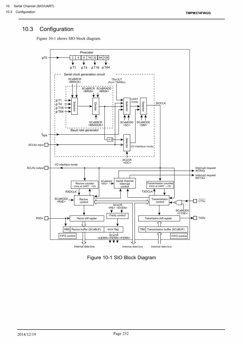
10.3 ConfigurationFigure 10-1 shows SIO block diagram.
φT0
fsys
T1T4T16T64
T1
SCxBRCR<BR0CK>
TBxOUT (from TMRBx)
SCxBRCR<BRADDE>
SCxCR <IOC>
SIOCLK
SCxMOD0 <RXE>
SCxMOD0 <WU>
TXDCLK
SCxCR <PE> <EVEN>
SCxMOD0 <CTSE>
SCxMOD0 <SC>
SCxMOD0 <SM>
SCxBRCR<BR0S>
SCxBRADD<BR0K>
Prescaler
UART mode
SCLKx input
SCLKx output
RXDx TXDx
Interrupt request INTRXx Interrupt request INTTXx
2
SCxCR <OERR><PERR><FERR>
I/O interface mode
CTSx
RXDCLK
2 4 8 16 32 64 128
T4 T16 T64
Baud rate generator
I/O interface mode
Transmission counter (Only at UART : ÷16)
Serial channel Interrupt control
Transmission control
Recive control
Recive shift register
TB8 Transmission buffer (SCxBUF) RB8 Recive buffer (SCxBUF)
Parity control
FIFO control
error flag
FIFO control
Internal data bus Internal data bus Internal data bus
Selector
Selector
Selector
Selector
Transmission shift register
Divider
Serial clock generation circuit
Recive counter (Only at UART : ÷16)
Figure 10-1 SIO Block Diagram
TMPM374FWUG
10. Serial Channel (SIO/UART)
10.3 Configuration
Page 2322014/12/19

10.4 Registers Description
10.4.1 Registers List in Each Channel
The each channel registers and addresses are shown below.
Channel x Base Address
Channel0 0x4002_0080
Channel1 0x4002_00C0
Channel3 0x4002_0140
Register name (x=0,1,3) Address (Base+)
Enable register SCxEN 0x0000
Buffer register SCxBUF 0x0004
Control register SCxCR 0x0008
Mode control register 0 SCxMOD0 0x000C
Baud rate generator control register SCxBRCR 0x0010
Baud rate generator control register 2 SCxBRADD 0x0014
Mode control register 1 SCxMOD1 0x0018
Mode control register 2 SCxMOD2 0x001C
RX FIFO configuration register SCxRFC 0x0020
TX FIFO configuration register SCxTFC 0x0024
RX FIFO status register SCxRST 0x0028
TX FIFO status register SCxTST 0x002C
FIFO configuration register SCxFCNF 0x0030
Note:Do not modify any control register when data is being transmitted or received.
TMPM374FWUG
Page 233 2014/12/19
10.4.2 SCxEN (Enable Register)
31 30 29 28 27 26 25 24
bit symbol - - - - - - - -
After reset 0 0 0 0 0 0 0 0
23 22 21 20 19 18 17 16
bit symbol - - - - - - - -
After reset 0 0 0 0 0 0 0 0
15 14 13 12 11 10 9 8
bit symbol - - - - - - - -
After reset 0 0 0 0 0 0 0 0
7 6 5 4 3 2 1 0
bit symbol - - - - - - - SIOE
After reset 0 0 0 0 0 0 0 0
Bit Bit Symbol Type Function
31-1 − R Read as 0.
0 SIOE R/W SIO operation0: Disabled1: EnabledSpecified the SIO operation.To use the SIO, set <SIOE> = "1".When the operation is disabled, no clock is supplied to the other registers in the SIO module. This can re-duce the power consumption.If the SIO operation is executed and then disabled, the settings will be maintained in each register exceptfor SCxTFC<TIL[1:0]>.
Note:When SCxEN<SIOE> is cleared to "0" (disable SIO operation) or the operation mode transits toIDLE mode by setting SCxMOD1<I2S0> to "0", it is necessary to reset SCxTFC.
TMPM374FWUG
10. Serial Channel (SIO/UART)
10.4 Registers Description
Page 2342014/12/19

10.4.3 SCxBUF (Buffer Register)
SCxBUF works as a transmit buffer or FIFO for write operation and as a receive buffer or FIFO for read op-eration.
31 30 29 28 27 26 25 24
bit symbol - - - - - - - -
After reset 0 0 0 0 0 0 0 0
23 22 21 20 19 18 17 16
bit symbol - - - - - - - -
After reset 0 0 0 0 0 0 0 0
15 14 13 12 11 10 9 8
bit symbol - - - - - - - -
After reset 0 0 0 0 0 0 0 0
7 6 5 4 3 2 1 0
bit symbol TB / RB
After reset 0 0 0 0 0 0 0 0
Bit Bit Symbol Type Function
31-8 − R Read as 0.
7-0 TB[7:0] / RB[7:0]
R/W [write] TB : Transmit buffer / FIFO[read] RB : Receive buffer / FIFO
TMPM374FWUG
Page 235 2014/12/19

10.4.4 SCxCR (Control Register)
31 30 29 28 27 26 25 24
bit symbol - - - - - - - -
After reset 0 0 0 0 0 0 0 0
23 22 21 20 19 18 17 16
bit symbol - - - - - - - -
After reset 0 0 0 0 0 0 0 0
15 14 13 12 11 10 9 8
bit symbol - - - - - - - -
After reset 0 0 0 0 0 0 0 0
7 6 5 4 3 2 1 0
bit symbol RB8 EVEN PE OERR PERR FERR SCLKS IOC
After reset 0 0 0 0 0 0 0 0
Bit Bit Symbol Type Function
31-8 − R Read as 0.
7 RB8 R Receive data bit 8 (For UART)9th bit of the received data in the 9 bits UART mode.
6 EVEN R/W Parity (For UART)0: Odd1: EvenSelects even or odd parity."0" : odd parity, "1" : even parity.The parity bit may be used only in the 7- or 8-bit UART mode.
5 PE R/W Add parity (For UART)0: Disabled1: EnabledControls enabling/ disabling parity.The parity bit may be used only in the 7- or 8-bit UART mode.
4 OERR R Overrun error flag (Note)0: Normal operation1: Error
3 PERR R Parity / Under-run error flag (Note)0: Normal operation1: Error
2 FERR R Framing error flag (Note)0: Normal operation1: Error
1 SCLKS R/W Selects input clock edge for data transmission and reception. (For I/O Interface)0: Data in the transmit buffer is sent to TXDx pin one bit at a time on the falling edge of SCLKx.Data from RXDx pin is received in the receive buffer one bit at a time on the rising edge of SCLKx.In this case, the SCLK starts from high level.1: Data in the transmit buffer is sent to TXDx pin one bit at a time on the rising edge of SCLKx.Data from RXDx pin is received in the receive buffer one bit at a time on the falling edge of SCLKx.In this case, the SCLK starts from low level. Set to "0" in the clock output mode.
0 IOC R/W Selecting clock (For I/O Interface)0: Baud rate generator1: SCLK pin input
Note:Any error flag (OERR, PERR, FERR) is cleared to "0" when read.
TMPM374FWUG
10. Serial Channel (SIO/UART)
10.4 Registers Description
Page 2362014/12/19
10.4.5 SCxMOD0 (Mode Control Register 0)
31 30 29 28 27 26 25 24
bit symbol - - - - - - - -
After reset 0 0 0 0 0 0 0 0
23 22 21 20 19 18 17 16
bit symbol - - - - - - - -
After reset 0 0 0 0 0 0 0 0
15 14 13 12 11 10 9 8
bit symbol - - - - - - - -
After reset 0 0 0 0 0 0 0 0
7 6 5 4 3 2 1 0
bit symbol TB8 CTSE RXE WU SM SC
After reset 0 0 0 0 0 0 0 0
Bit Bit Symbol Type Function
31-8 − R Read as 0.
7 TB8 R/W Transmit data bit 8 (For UART)Writes the 9th bit of transmit data in the 9 bits UART mode.
6 CTSE R/W Handshake function control (For UART)0: CTS disabled1: CTS enabledControls handshake function.Setting "1" enables handshake function using CTS pin.
5 RXE R/W Receive control (Note1)(Note2)0: Disabled1: Enabled
4 WU R/W Wake-up function (For UART)0: Disabled1: EnabledThis function is available only at 9-bit UART mode. In other mode, this function has no meaning.In it is Enabled, Interrupt only when RB9 = "1" at 9-bit UART mode.
3-2 SM[1:0] R/W Specifies transfer mode.00: I/O interface mode01: 7-bit length UART mode10: 8-bit length UART mode11: 9-bit length UART mode
1-0 SC[1:0] R/W Serial transfer clock (For UART)00: Timer TBxOUT (Refer to Table 10-1)01: Baud rate generator10: Internal clock fsys11: External clock (SCLK input)(As for the I/O interface mode, the serial transfer clock can be set in the control register (SCxCR).
Note 1: With <RXE> set to "0", set each mode register (SCxMOD0, SCxMOD1 and SCxMOD2). Then set <RXE> to "1".Note 2: Do not stop the receive operation (by setting SCxMOD0<RXE> = "0") when data is being received.
TMPM374FWUG
Page 237 2014/12/19
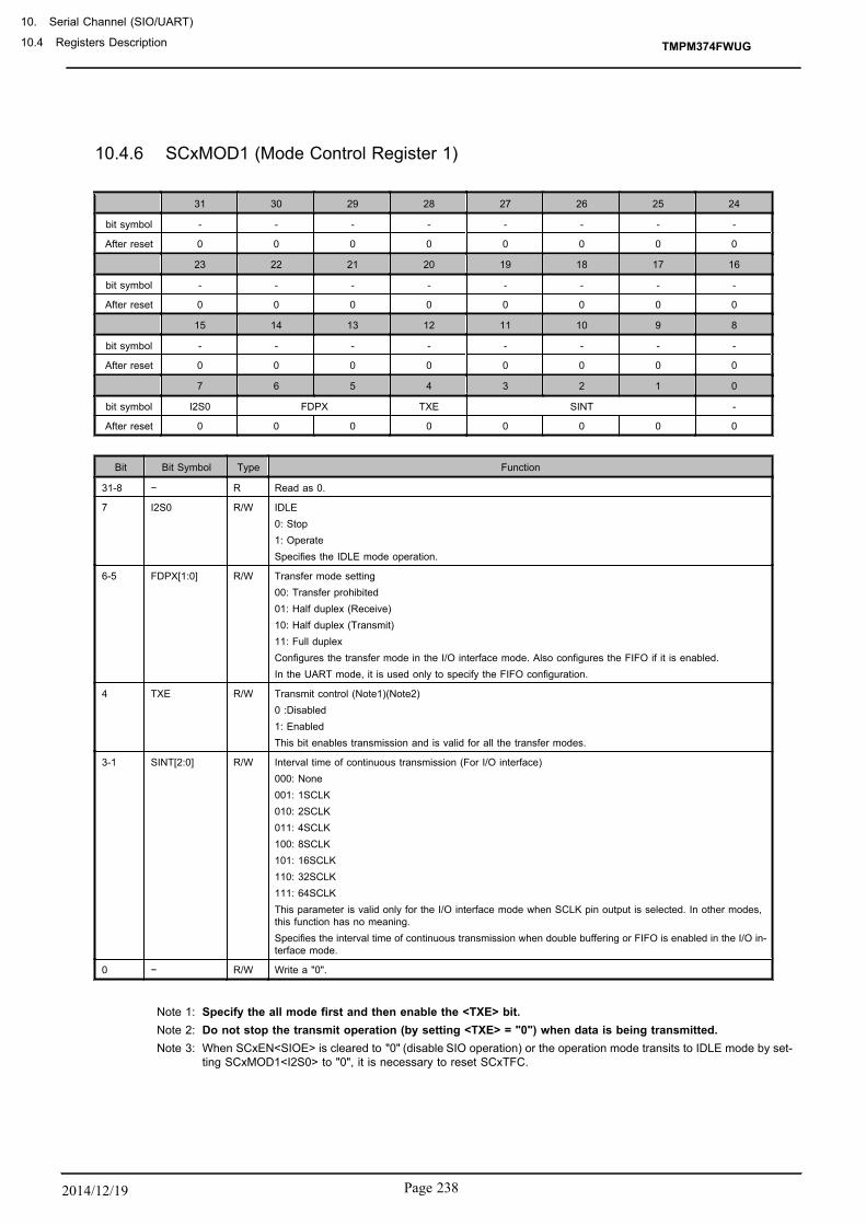
10.4.6 SCxMOD1 (Mode Control Register 1)
31 30 29 28 27 26 25 24
bit symbol - - - - - - - -
After reset 0 0 0 0 0 0 0 0
23 22 21 20 19 18 17 16
bit symbol - - - - - - - -
After reset 0 0 0 0 0 0 0 0
15 14 13 12 11 10 9 8
bit symbol - - - - - - - -
After reset 0 0 0 0 0 0 0 0
7 6 5 4 3 2 1 0
bit symbol I2S0 FDPX TXE SINT -
After reset 0 0 0 0 0 0 0 0
Bit Bit Symbol Type Function
31-8 − R Read as 0.
7 I2S0 R/W IDLE0: Stop1: OperateSpecifies the IDLE mode operation.
6-5 FDPX[1:0] R/W Transfer mode setting00: Transfer prohibited01: Half duplex (Receive)10: Half duplex (Transmit)11: Full duplexConfigures the transfer mode in the I/O interface mode. Also configures the FIFO if it is enabled.In the UART mode, it is used only to specify the FIFO configuration.
4 TXE R/W Transmit control (Note1)(Note2)0 :Disabled1: EnabledThis bit enables transmission and is valid for all the transfer modes.
3-1 SINT[2:0] R/W Interval time of continuous transmission (For I/O interface)000: None001: 1SCLK010: 2SCLK011: 4SCLK100: 8SCLK101: 16SCLK110: 32SCLK111: 64SCLKThis parameter is valid only for the I/O interface mode when SCLK pin output is selected. In other modes,this function has no meaning.Specifies the interval time of continuous transmission when double buffering or FIFO is enabled in the I/O in-terface mode.
0 − R/W Write a "0".
Note 1: Specify the all mode first and then enable the <TXE> bit.Note 2: Do not stop the transmit operation (by setting <TXE> = "0") when data is being transmitted.Note 3: When SCxEN<SIOE> is cleared to "0" (disable SIO operation) or the operation mode transits to IDLE mode by set-
ting SCxMOD1<I2S0> to "0", it is necessary to reset SCxTFC.
TMPM374FWUG
10. Serial Channel (SIO/UART)
10.4 Registers Description
Page 2382014/12/19
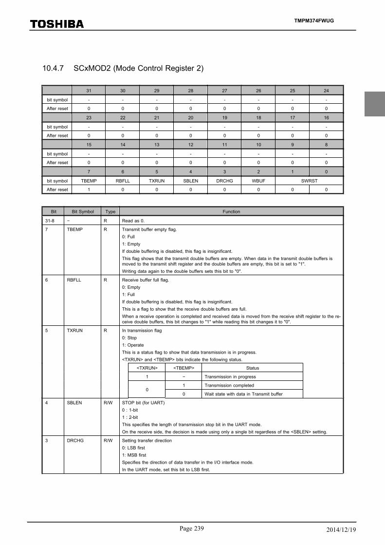
10.4.7 SCxMOD2 (Mode Control Register 2)
31 30 29 28 27 26 25 24
bit symbol - - - - - - - -
After reset 0 0 0 0 0 0 0 0
23 22 21 20 19 18 17 16
bit symbol - - - - - - - -
After reset 0 0 0 0 0 0 0 0
15 14 13 12 11 10 9 8
bit symbol - - - - - - - -
After reset 0 0 0 0 0 0 0 0
7 6 5 4 3 2 1 0
bit symbol TBEMP RBFLL TXRUN SBLEN DRCHG WBUF SWRST
After reset 1 0 0 0 0 0 0 0
Bit Bit Symbol Type Function
31-8 − R Read as 0.
7 TBEMP R Transmit buffer empty flag.0: Full1: EmptyIf double buffering is disabled, this flag is insignificant.This flag shows that the transmit double buffers are empty. When data in the transmit double buffers ismoved to the transmit shift register and the double buffers are empty, this bit is set to "1".Writing data again to the double buffers sets this bit to "0".
6 RBFLL R Receive buffer full flag.0: Empty1: FullIf double buffering is disabled, this flag is insignificant.This is a flag to show that the receive double buffers are full.When a receive operation is completed and received data is moved from the receive shift register to the re-ceive double buffers, this bit changes to "1" while reading this bit changes it to "0".
5 TXRUN R In transmission flag0: Stop1: OperateThis is a status flag to show that data transmission is in progress.<TXRUN> and <TBEMP> bits indicate the following status.
<TXRUN> <TBEMP> Status
1 − Transmission in progress
0
1 Transmission completed
0 Wait state with data in Transmit buffer
4 SBLEN R/W STOP bit (for UART)0 : 1-bit1 : 2-bitThis specifies the length of transmission stop bit in the UART mode.On the receive side, the decision is made using only a single bit regardless of the <SBLEN> setting.
3 DRCHG R/W Setting transfer direction0: LSB first1: MSB firstSpecifies the direction of data transfer in the I/O interface mode.In the UART mode, set this bit to LSB first.
TMPM374FWUG
Page 239 2014/12/19
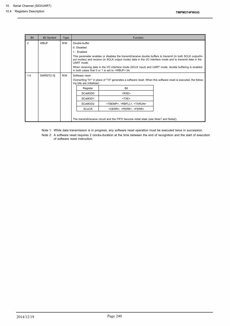
Bit Bit Symbol Type Function
2 WBUF R/W Double-buffer0: Disabled1 : EnabledThis parameter enables or disables the transmit/receive double buffers to transmit (in both SCLK output/in-put modes) and receive (in SCLK output mode) data in the I/O interface mode and to transmit data in theUART mode.When receiving data in the I/O interface mode (SCLK input) and UART mode, double buffering is enabledin both cases that 0 or 1 is set to <WBUF> bit.
1-0 SWRST[1:0] R/W Software resetOverwriting "01" in place of "10" generates a software reset. When this software reset is executed, the follow-ing bits are initialized :
Register Bit
SCxMOD0 <RXE>
SCxMOD1 <TXE>
SCxMOD2 <TBEMP>, <RBFLL>, <TXRUN>
SCxCR <OERR>, <PERR>, <FERR>
The transmit/receive circuit and the FIFO become initial state (see Note1 and Note2).
Note 1: While data transmission is in progress, any software reset operation must be executed twice in succession.Note 2: A software reset requires 2 clocks-duration at the time between the end of recognition and the start of execution
of software reset instruction.
TMPM374FWUG
10. Serial Channel (SIO/UART)
10.4 Registers Description
Page 2402014/12/19
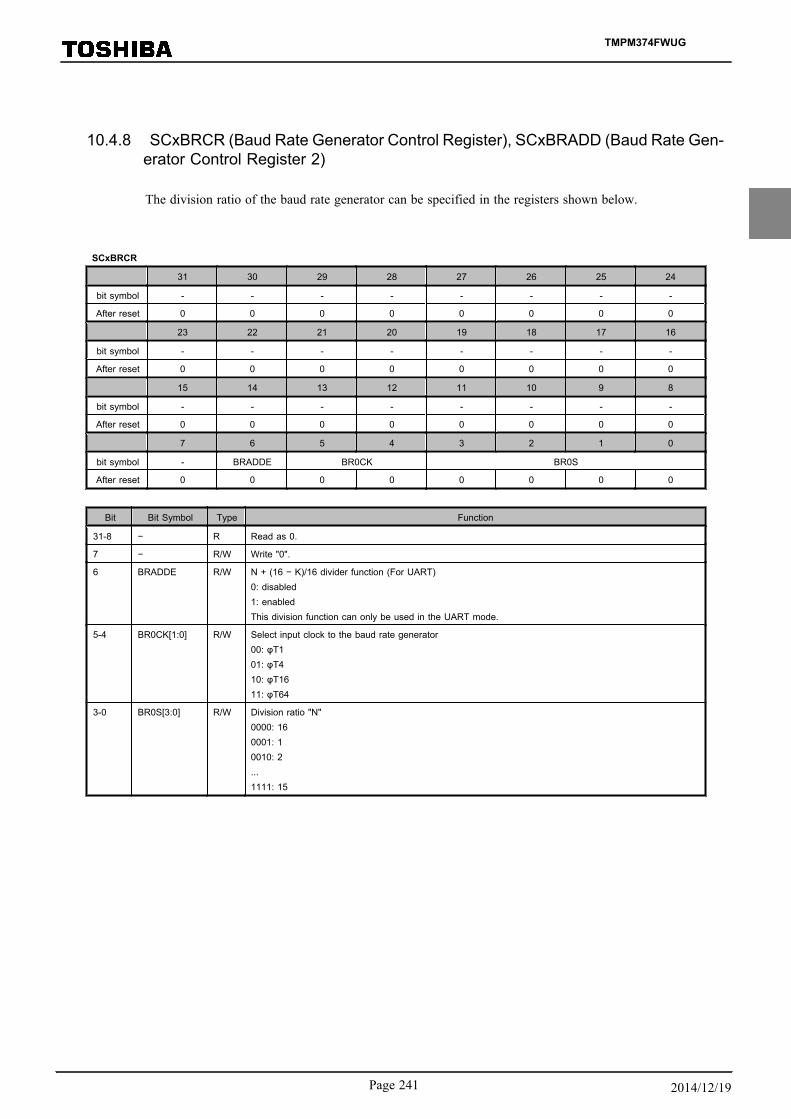
10.4.8 SCxBRCR (Baud Rate Generator Control Register), SCxBRADD (Baud Rate Gen-erator Control Register 2)
The division ratio of the baud rate generator can be specified in the registers shown below.
SCxBRCR
31 30 29 28 27 26 25 24
bit symbol - - - - - - - -
After reset 0 0 0 0 0 0 0 0
23 22 21 20 19 18 17 16
bit symbol - - - - - - - -
After reset 0 0 0 0 0 0 0 0
15 14 13 12 11 10 9 8
bit symbol - - - - - - - -
After reset 0 0 0 0 0 0 0 0
7 6 5 4 3 2 1 0
bit symbol - BRADDE BR0CK BR0S
After reset 0 0 0 0 0 0 0 0
Bit Bit Symbol Type Function
31-8 − R Read as 0.
7 − R/W Write "0".
6 BRADDE R/W N + (16 − K)/16 divider function (For UART)0: disabled1: enabledThis division function can only be used in the UART mode.
5-4 BR0CK[1:0] R/W Select input clock to the baud rate generator00: φT101: φT410: φT1611: φT64
3-0 BR0S[3:0] R/W Division ratio "N"0000: 160001: 10010: 2...1111: 15
TMPM374FWUG
Page 241 2014/12/19

SCxBRADD
31 30 29 28 27 26 25 24
bit symbol - - - - - - - -
After reset 0 0 0 0 0 0 0 0
23 22 21 20 19 18 17 16
bit symbol - - - - - - - -
After reset 0 0 0 0 0 0 0 0
15 14 13 12 11 10 9 8
bit symbol - - - - - - - -
After reset 0 0 0 0 0 0 0 0
7 6 5 4 3 2 1 0
bit symbol - - - - BR0K
After reset 0 0 0 0 0 0 0 0
Bit Bit Symbol Type Function
31-4 − R Read as 0.
3-0 BR0K[3:0] R/W Specify K for the "N + (16 − K)/16" division (For UART)0000: Prohibited0001: K = 10010: K = 2...1111: K = 15
Table 10-2 lists the settings of baud rate generator division ratio.
Table 10-2 Setting division ratio
<BRADDE> = "0"<BRADDE> = "1" (Note1)
(Only UART mode)
<BR0S> Specify "N" (Note2) (Note3)
<BR0K> No setting required Specify "K" (Note4)
Division ratio Divide by N N + (16 − K)16
Note 1: To use the "N + (16 - K)/16" division function, be sure to set <BRADDE> to "1" after setting the Kvalue to <BR0K>. The "N + (16 - K)/16" division function can only be used in the UART mode.
Note 2: As a division ratio, 1 ("0001") or 16 ("0000") can not be applied to N when using the "N + (16 - K)/16" division function in the UART mode.
Note 3: The division ratio "1" of the baud rate generator can be specified only when the double bufferingis used in the I/O interface mode.
Note 4: Specifying "K = 0" is prohibited.
TMPM374FWUG
10. Serial Channel (SIO/UART)
10.4 Registers Description
Page 2422014/12/19

10.4.9 SCxFCNF (FIFO Configuration Register)
31 30 29 28 27 26 25 24
bit symbol - - - - - - - -
After reset 0 0 0 0 0 0 0 0
23 22 21 20 19 18 17 16
bit symbol - - - - - - - -
After reset 0 0 0 0 0 0 0 0
15 14 13 12 11 10 9 8
bit symbol - - - - - - - -
After reset 0 0 0 0 0 0 0 0
7 6 5 4 3 2 1 0
bit symbol - - - RFST TFIE RFIE RXTXCNT CNFG
After reset 0 0 0 0 0 0 0 0
Bit Bit Symbol Type Function
31-8 - R Read as 0
7-5 - R/W Be sure to write "000"
4 RFST R/W Bytes used in RX FIFO0:Maximum1:Same as FILL level of RX FIFOWhen RX FIFO is enabled, the number of RX FIFO bytes to be used is selected (Note1)0: The maximun number of bytes of the FIFO configured (see also <CNFG>).1: Same as the fill level for receive interrupt generation specified by SCxRFC <RIL[1:0]>
3 TFIE R/W TX interrupt for TX FIFO0: Disabled1: EnabledWhen TX FIFO is enabled, transmit interrupts are enabled or disabled by this parameter.
2 RFIE R/W RX interrupt for RX FIFO0: Disabled1: EnabledWhen RX FIFO is enabled, receive interrupts are enabled or disabled by this parameter.
1 RXTXCNT R/W Automatic disable of <RXE>/<TXE>0: None1: Auto disabledControls automatic disabling of transmission and reception.Setting "1" enables to operate as follows
Half duplex RX When receive shift register, the receive buffer and the RX FIFO are filled,SCxMOD0<RXE> is automatically set to "0" to inhibit further reception.
Half duplex TX When the TX FIFO, the transmit buffer and the transmit shift register is empty,SCxMOD1<TXE> is automatically set to "0" to inhibit further transmission.
Full duplex When either of the above two conditions is satisfied, <TXE>/<RXE> are automat-ically set to "0" to inhibit further transmission and reception.
0 CNFG R/W Enables FIFO (Note2)0: Disabled1: EnabledIf enabled, the SCxMOD1 <FDPX[1:0]> setting automatically configures FIFO as follows:(The type of TX/RX can be specified in the mode control register 1 SCxMOD1<FDPX[1:0]>).
Half duplex RX RX FIFO 4byte
Half duplex TX TX FIFO 4byte
Full duplex RX FIFO 2byte + TX FIFO 2byte
Note 1: Regarding TX FIFO, the maximum number of bytes being configured is always available. The availablenumber of bytes is the bytes already written to the TX FIFO.
Note 2: The FIFO can not use in 9bit UART mode.
TMPM374FWUG
Page 243 2014/12/19

10.4.10 SCxRFC (RX FIFO Configuration Register)
31 30 29 28 27 26 25 24
bit symbol - - - - - - - -
After reset 0 0 0 0 0 0 0 0
23 22 21 20 19 18 17 16
bit symbol - - - - - - - -
After reset 0 0 0 0 0 0 0 0
15 14 13 12 11 10 9 8
bit symbol - - - - - - - -
After reset 0 0 0 0 0 0 0 0
7 6 5 4 3 2 1 0
bit symbol RFCS RFIS - - - - RIL
After reset 0 0 0 0 0 0 0 0
Bit Bit Symbol Type Function
31-8 − R Read as 0.
7 RFCS W RX FIFO clear (Note)1: Clears RX FIFOWhen SCxRFC<RFCS> is set to "1", the receive FIFO is cleared and SCxRST<RLVL> is "000". And alsothe read pointer is initialized.
6 RFIS R/W Select interrupt generation condition0: An interrupt is generated when the data reaches to the specified fill level.1: An interrupt is generated when the data reaches to the specified fill level or the data exceeds the speci-fied fill level at the time data is read.
5-2 − R Read as 0.
1-0 RIL[1:0] R/W FIFO fill level to generate RX interrupts
Half duplex Full duplex
00 4byte 2byte
01 1byte 1byte
10 2byte 2byte
11 3byte 1byte
Note:To use TX/RX FIFO buffer, TX/RX FIFO must be cleared after setting the SIO transfer mode (half du-plex/full duplex) and enabling FIFO (SCxFCNF<CNFG> = "1").
TMPM374FWUG
10. Serial Channel (SIO/UART)
10.4 Registers Description
Page 2442014/12/19

10.4.11 SCxTFC (TX FIFO Configuration Register) (Note2)
31 30 29 28 27 26 25 24
bit symbol - - - - - - - -
After reset 0 0 0 0 0 0 0 0
23 22 21 20 19 18 17 16
bit symbol - - - - - - - -
After reset 0 0 0 0 0 0 0 0
15 14 13 12 11 10 9 8
bit symbol - - - - - - - -
After reset 0 0 0 0 0 0 0 0
7 6 5 4 3 2 1 0
bit symbol TFCS TFIS - - - - TIL
After reset 0 0 0 0 0 0 0 0
Bit Bit Symbol Type Function
31-8 − R Read as 0.
7 TFCS W TX FIFO clear (Note 1)1: Clears TX FIFO.When SCxTST<TFCS> is set to "1", the transmit FIFO is cleared and SCxRST<TLVL> is "000". And alsothe write pointer is initialized.
6 TFIS R/W Selects interrupt generation condition.0: An interrupt is generated when the data reaches to the specified fill level.1: An interrupt is generated when the data reaches to the specified fill level or the data can not reach thespecified fill level at the time new data is read.
5-2 − R Read as 0.
1-0 TIL[1:0] R/W FIFO fill level to generate TX interrupts.
Other than fullduplex Full duplex
00 Empty Empty
01 1 byte 1 byte
10 2 byte Empty
11 3 byte 1 byte
Note 1: To use TX/RX FIFO buffer, TX/RX FIFO must be cleared after setting the SIO transfer mode (half duplex/full duplex) and enabling FIFO (SCxFCNF<CNFG> = "1").
Note 2: After you perform the following operations, configure the SCxTFC register again.SCxEN<SIOE> = "0" (SIO operation stop)Conditions are as follows:SCxMOD1<I2S0> = "0" (operation is prohibited in IDLE mode) and releasingthe low power consumption mode which started by the WFI (Wait For Interrupt) instruction.
TMPM374FWUG
Page 245 2014/12/19

10.4.12 SCxRST (RX FIFO Status Register)
31 30 29 28 27 26 25 24
bit symbol - - - - - - - -
After reset 0 0 0 0 0 0 0 0
23 22 21 20 19 18 17 16
bit symbol - - - - - - - -
After reset 0 0 0 0 0 0 0 0
15 14 13 12 11 10 9 8
bit symbol - - - - - - - -
After reset 0 0 0 0 0 0 0 0
7 6 5 4 3 2 1 0
bit symbol ROR - - - - RLVL
After reset 0 0 0 0 0 0 0 0
Bit Bit Symbol Type Function
31-8 − R Read as 0.
7 ROR R RX FIFO Overrun (Note)0: Not generated1: Generated
6-3 − R Read as 0.
2-0 RLVL[2:0] R Status of RX FIFO fill level.000: Empty001: 1 byte010: 2 byte011: 3 byte100: 4 byte
Note:The <ROR> bit is cleared to "0" when receive data is read from the SCxBUF register.
TMPM374FWUG
10. Serial Channel (SIO/UART)
10.4 Registers Description
Page 2462014/12/19

10.4.13 SCxTST (TX FIFO Status Register)
31 30 29 28 27 26 25 24
bit symbol - - - - - - - -
After reset 0 0 0 0 0 0 0 0
23 22 21 20 19 18 17 16
bit symbol - - - - - - - -
After reset 0 0 0 0 0 0 0 0
15 14 13 12 11 10 9 8
bit symbol - - - - - - - -
After reset 0 0 0 0 0 0 0 0
7 6 5 4 3 2 1 0
bit symbol TUR - - - - TLVL
After reset 1 0 0 0 0 0 0 0
Bit Bit Symbol Type Function
31-8 − R Read as 0.
7 TUR R TX FIFO under run (Note)0: Not generated1: Generated.
6-3 − R Read as 0.
2-0 TLVL[2:0] R Status of TX FIFO fill level.000: Empty001: 1 byte010: 2 byte011: 3 byte100: 4 byte
Note:The <TUR> bit is cleared to "0" when transmit data is written to the SCxBUF register.
TMPM374FWUG
Page 247 2014/12/19

10.5 Operation in Each ModeTable 10-3 shows the modes and data formats.
Table 10-3 Mode and Data format
Mode Mode type Data length Transfer directionSpecifies
whether to useparity bits.
STOP bit length (transmit)
Mode 0Synchronous communication
mode(IO interface mode)
8 bit LSB first/MSB first - -
Mode 1Asynchronous communica-
tion mode(UART mode)
7 bit
LSB first
ο
1 bit or 2 bitMode 2 8 bit ο
Mode 3 9 bit ×
Mode 0 is a synchronous communication and can be used to extend I/O. This mode transmits and receives datain synchronization with SCLK. SCLK can be used for both input and output.
The direction of data transfer can be selected from LSB first and MSB first. This mode is not allowed either touse parity bits or STOP bits.
The mode 1, mode 2 and mode 3 are asynchronous modes and the transfer direction is fixed to the LSB first.
Parity bits can be added in the mode 1 and mode 2. The mode 3 has a wakeup function in which the master con-troller can start up slave controllers via the serial link (multi-controller system).
STOP bit in transmission can be selected from 1 bit and 2 bits. The STOP bit length in reception is fixed to aone bit.
TMPM374FWUG
10. Serial Channel (SIO/UART)
10.5 Operation in Each Mode
Page 2482014/12/19

10.6 Data Format
10.6.1 Data Format List
Figure 10-2 shows data format.
● Mode1 (7bits UART mode)
bit 0 1 2 3 4 5 6 stopstartWithout parity
bit 0 1 2 3 4 5 6 parity stopstartWith parity
● Mode2 (8bits UART mode)
bit 0 1 2 3 4 5 6start 7 stopWithout parity
bit 0 1 2 3 4 5 6 7 parity stopstartWith parity
stopbit 0 1 2 3 4 5 6start 7 8
bit 0 1 2 3 4 5 6 7 bit 8 stop (Wake-up)start
● Mode3 (9bits UART mode)
bit 8 = 1 represents address. (select code)bit 8 = 0 represents data.
1bit 0 2 3 4 5 6
● Mode0 (I/O interface mode) / LSB first
Transmission direction
7
6bit 7 5 4 3 2 1
● Mode0 (I/O interface mode ) / MSB first
Transmission direction
0
Figure 10-2 Data Format
TMPM374FWUG
Page 249 2014/12/19

10.6.2 Parity Control
The parity bit can be added only in the 7 or 8-bit UART mode.
Setting "1" to SCxCR<PE> enables the parity.
The <EVEN> bit of SCxCR selects either even or odd parity.
10.6.2.1 Transmission
Upon data transmission, the parity control circuit automatically generates the parity with the data in thetransmit buffer.
After data transmission is complete, the parity bit will be stored in SCxBUF<TB7> in the 7-bit UARTmode and SCxMOD0<TB8> in the 8-bit UART mode.
The <PE> and <EVEN> settings must be completed before data is written to the transmit buffer.
10.6.2.2 Receiving Data
If the received data is moved from the receive shift register to the receive buffer, a parity is generated.
In the 7-bit UART mode, the generated parity is compared with the parity stored in SCxBUF<RB7>,while in the 8-bit UART mode, it is compared with the one in SCxCR<RB8>.
If there is any difference, a parity error occurs and the <PERR> of the SCxCR register is set to "1".
In use of the FIFO, <PERR> indicates that a parity error was generated in one of the received data.
10.6.3 STOP Bit Length
The length of the STOP bit in the UART transmission mode can be selected from one bit or two bits by set-ting the SCxMOD2<SBLEN>. The length of the STOP bit data is determined as one-bit when it is received re-gardless of the setting of this bit.
TMPM374FWUG
10. Serial Channel (SIO/UART)
10.6 Data Format
Page 2502014/12/19

10.7 Clock Control
10.7.1 Prescaler
There is a 7-bit prescaler to divide a prescaler input clock ΦT0 by 2, 8, 32 and 128.
Use the CGSYSCR register in the clock/mode control block to select the input clock ΦT0 of the prescaler.
The prescaler becomes active only when the baud rate generator is selected as a transfer clock bySCxMOD0<SC[1:0]> = "01".
Table 10-4 show the resolution of the input clock to the baud rate generator.
Table 10-4 Clock Resolution to the Baud Rate Generator fc = 80 MHz
peripheral clockselection
CGSYSCR<FPSEL>
Clock gearvalue
CGSYSCR<GEAR[2:0]>
Prescaler clock se-lection
CGSYSCR<PRCK[2:0]>
Prescaler output clock resolution
φT1 φT4 φT16 φT64
0 (fgear)
000 (fc)
000 (fperiph/1) fc/21 (0.025 μs) fc/23 (0.1 μs) fc/25 (0.4 μs) fc/27 (1.6 μs)
001 (fperiph/2) fc/22 (0.05 μs) fc/24 (0.2 μs) fc/26 (0.8 μs) fc/28 (3.2 μs)
010 (fperiph/4) fc/23 (0.1 μs) fc/25 (0.4 μs) fc/27 (1.6 μs) fc/29 (6.4 μs)
011 (fperiph/8) fc/24 (0.2 μs) fc/26 (0.8 μs) fc/28 (3.2 μs) fc/210 (12.8 μs)
100 (fperiph/16) fc/25 (0.4 μs) fc/27 (1.6 μs) fc/29 (6.4 μs) fc/211 (25.6 μs)
101 (fperiph/32) fc/26 (0.8 μs) fc/28 (3.2 μs) fc/210 (12.8 μs) fc/212 (51.2 μs)
100 (fc/2)
000 (fperiph/1) fc/22 (0.05 μs) fc/24 (0.2 μs) fc/26 (0.8 μs) fc/28 (3.2 μs)
001 (fperiph/2) fc/23 (0.1 μs) fc/25 (0.4 μs) fc/27 (1.6 μs) fc/29 (6.4 μs)
010 (fperiph/4) fc/24 (0.2 μs) fc/26 (0.8 μs) fc/28 (3.2 μs) fc/210 (12.8 μs)
011 (fperiph/8) fc/25 (0.4 μs) fc/27 (1.6 μs) fc/29 (6.4 μs) fc/211 (25.6 μs)
100 (fperiph/16) fc/26 (0.8 μs) fc/28 (3.2 μs) fc/210 (12.8 μs) fc/212 (51.2 μs)
101 (fperiph/32) fc/27 (1.6 μs) fc/29 (6.4 μs) fc/211 (25.6 μs) fc/213 (102.4 μs)
101 (fc/4)
000 (fperiph/1) fc/23 (0.1 μs) fc/25 (0.4 μs) fc/27 (1.6 μs) fc/29 (6.4 μs)
001 (fperiph/2) fc/24 (0.2 μs) fc/26 (0.8 μs) fc/28 (3.2 μs) fc/210 (12.8 μs)
010 (fperiph/4) fc/25 (0.4 μs) fc/27 (1.6 μs) fc/29 (6.4 μs) fc/211 (25.6 μs)
011 (fperiph/8) fc/26 (0.8 μs) fc/28 (3.2 μs) fc/210 (12.8 μs) fc/212 (51.2 μs)
100 (fperiph/16) fc/27 (1.6 μs) fc/29 (6.4 μs) fc/211 (25.6 μs) fc/213 (102.4 μs)
101 (fperiph/32) fc/28 (3.2 μs) fc/210 (12.8 μs) fc/212 (51.2 μs) fc/214 (204.8 μs)
110 (fc/8)
000 (fperiph/1) fc/24 (0.2 μs) fc/26 (0.8 μs) fc/28 (3.2 μs) fc/210 (12.8 μs)
001 (fperiph/2) fc/25 (0.4 μs) fc/27 (1.6 μs) fc/29 (6.4 μs) fc/211 (25.6 μs)
010 (fperiph/4) fc/26 (0.8 μs) fc/28 (3.2 μs) fc/210 (12.8 μs) fc/212 (51.2 μs)
011 (fperiph/8) fc/27 (1.6 μs) fc/29 (6.4 μs) fc/211 (25.6 μs) fc/213 (102.4 μs)
100 (fperiph/16) fc/28 (3.2 μs) fc/210 (12.8 μs) fc/212 (51.2 μs) fc/214 (204.8 μs)
101 (fperiph/32) fc/29 (6.4 μs) fc/211 (25.6 μs) fc/213 (102.4 μs) fc/215 (409.6 μs)
111 (fc/16)
000 (fperiph/1) fc/25 (0.4 μs) fc/27 (1.6 μs) fc/29 (6.4 μs) fc/211 (25.6 μs)
001 (fperiph/2) fc/26 (0.8 μs) fc/28 (3.2 μs) fc/210 (12.8 μs) fc/212 (51.2 μs)
010 (fperiph/4) fc/27 (1.6 μs) fc/29 (6.4 μs) fc/211 (25.6 μs) fc/213 (102.4 μs)
011 (fperiph/8) fc/28 (3.2 μs) fc/210 (12.8 μs) fc/212 (51.2 μs) fc/214 (204.8 μs)
100 (fperiph/16) fc/29 (6.4 μs) fc/211 (25.6 μs) fc/213 (102.4 μs) fc/215 (409.6 μs)
101 (fperiph/32) fc/210 (12.8 μs) fc/212 (51.2 μs) fc/214 (204.8 μs) fc/216 (819.2 μs)
TMPM374FWUG
Page 251 2014/12/19

Table 10-4 Clock Resolution to the Baud Rate Generator fc = 80 MHz
peripheral clockselection
CGSYSCR<FPSEL>
Clock gearvalue
CGSYSCR<GEAR[2:0]>
Prescaler clock se-lection
CGSYSCR<PRCK[2:0]>
Prescaler output clock resolution
φT1 φT4 φT16 φT64
1 (fc)
000 (fc)
000 (fperiph/1) fc/21 (0.025 μs) fc/23 (0.1 μs) fc/25 (0.4 μs) fc/27 (1.6 μs)
001 (fperiph/2) fc/22 (0.05 μs) fc/24 (0.2 μs) fc/26 (0.8 μs) fc/28 (3.2 μs)
010 (fperiph/4) fc/23 (0.1 μs) fc/25 (0.4 μs) fc/27 (1.6 μs) fc/29 (6.4 μs)
011 (fperiph/8) fc/24 (0.2 μs) fc/26 (0.8 μs) fc/28 (3.2 μs) fc/210 (12.8 μs)
100 (fperiph/16) fc/25 (0.4 μs) fc/27 (1.6 μs) fc/29 (6.4 μs) fc/211 (25.6 μs)
101 (fperiph/32) fc/26 (0.8 μs) fc/28 (3.2 μs) fc/210 (12.8 μs) fc/212 (51.2 μs)
100 (fc/2)
000 (fperiph/1) − fc/23 (0.1 μs) fc/25 (0.4 μs) fc/27 (1.6 μs)
001 (fperiph/2) fc/22 (0.05 μs) fc/24 (0.2 μs) fc/26 (0.8 μs) fc/28 (3.2 μs)
010 (fperiph/4) fc/23 (0.1 μs) fc/25 (0.4 μs) fc/27 (1.6 μs) fc/29 (6.4 μs)
011 (fperiph/8) fc/24 (0.2 μs) fc/26 (0.8 μs) fc/28 (3.2 μs) fc/210 (12.8 μs)
100 (fperiph/16) fc/25 (0.4 μs) fc/27 (1.6 μs) fc/29 (6.4 μs) fc/211 (25.6 μs)
101 (fperiph/32) fc/26 (0.8 μs) fc/28 (3.2 μs) fc/210 (12.8 μs) fc/212 (51.2 μs)
101 (fc/4)
000 (fperiph/1) − fc/23 (0.1 μs) fc/25 (0.4 μs) fc/27 (1.6 μs)
001 (fperiph/2) − fc/24 (0.2 μs) fc/26 (0.8 μs) fc/28 (3.2 μs)
010 (fperiph/4) fc/23 (0.1 μs) fc/25 (0.4 μs) fc/27 (1.6 μs) fc/29 (6.4 μs)
011 (fperiph/8) fc/24 (0.2 μs) fc/26 (0.8 μs) fc/28 (3.2 μs) fc/210 (12.8 μs)
100 (fperiph/16) fc/25 (0.4 μs) fc/27 (1.6 μs) fc/29 (6.4 μs) fc/211 (25.6 μs)
101 (fperiph/32) fc/26 (0.8 μs) fc/28 (3.2 μs) fc/210 (12.8 μs) fc/212 (51.2 μs)
110 (fc/8)
000 (fperiph/1) − − fc/25 (0.4 μs) fc/27 (1.6 μs)
001 (fperiph/2) − fc/24 (0.2 μs) fc/26 (0.8 μs) fc/28 (3.2 μs)
010 (fperiph/4) − fc/25 (0.4 μs) fc/27 (1.6 μs) fc/29 (6.4 μs)
011 (fperiph/8) fc/24 (0.2 μs) fc/26 (0.8 μs) fc/28 (3.2 μs) fc/210 (12.8 μs)
100 (fperiph/16) fc/25 (0.4 μs) fc/27 (1.6 μs) fc/29 (6.4 μs) fc/211 (25.6 μs)
101 (fperiph/32) fc/26 (0.8 μs) fc/28 (3.2 μs) fc/210 (12.8 μs) fc/212 (51.2 μs)
111 (fc/16)
000 (fperiph/1) − − fc/25 (0.4 μs) fc/27 (1.6 μs)
001 (fperiph/2) − − fc/26 (0.8 μs) fc/28 (3.2 μs)
010 (fperiph/4) − fc/25 (0.4 μs) fc/27 (1.6 μs) fc/29 (6.4 μs)
011 (fperiph/8) − fc/26 (0.8 μs) fc/28 (3.2 μs) fc/210 (12.8 μs)
100 (fperiph/16) fc/25 (0.4 μs) fc/27 (1.6 μs) fc/29 (6.4 μs) fc/211 (25.6 μs)
101 (fperiph/32) fc/26 (0.8 μs) fc/28 (3.2 μs) fc/210 (12.8 μs) fc/212 (51.2 μs)
Note 1: The prescaler output clock φTn must be selected so that the relationship "φTn ≤ fsys / 2" is satisfied(so that φTn is slower than fsys).
Note 2: Do not change the clock gear while SIO is operating.Note 3: The dashes in the above table indicate that the setting is prohibited.
TMPM374FWUG
10. Serial Channel (SIO/UART)
10.7 Clock Control
Page 2522014/12/19

10.7.2 Serial Clock Generation Circuit
The serial clock circuit is a block to generate transmit and receive clocks (SIOCLK) and consists of the cir-cuits in which clocks can be selected by the settings of the baud rates generator and modes.
10.7.2.1 Baud Rate Generator
The baud rate generator generates transmit and receive clocks to determine the serial channel transferrate.
(1) Baud Rate Generator input clock
The input clock of the baud rate generator is selected from the prescaler outputs divided by 2, 8,32 and 128.
This input clock is selected by setting the SCxBRCR<BRCK>.
(2) Baud Rate Generator output clock
The frequency division ratio of the output clock in the baud rate generator is set by SCxBRCRand SCxBRADD.
The following frequency divide ratios can be used; 1/N frequency division in the I/O interfacemode ,either 1/N or N + (16-K)/16 in the UART mode.
The table below shows the frequency division ratio which can be selected.
ModeDivide Function SettingSCxBRCR<BRADDE>
Divide by NSCxBRCR<BR0S>
Divide by KSCxBRADD<BR0K>
I/O interface Divide by N 1 to 16 (Note) -
UART
Divide by N 1 to 16 -
N + (16-K)/16 division 2 to 15 1 to 15
Note:1/N (N=1)frequency division ratio can be used only when a double buffer is enabled.
TMPM374FWUG
Page 253 2014/12/19

10.7.2.2 Clock Selection Circuit
A clock can be selected by setting the modes and the register.
Modes can be specified by setting the SCxMOD0<SM>.
The input clock in I/O interface mode is selected by setting SCxCR. The clock in UART mode is selec-ted by setting SCxMOD0<SC>.
(1) Transfer Clock in I/O interface mode
Table 10-5 shows clock selection in I/O interface mode.
Table 10-5 Clock Selection in I/O Interface Mode
ModeSCxMOD0<SM>
Input/Outputselection
SCxCR<IOC>
Clock edge selectionSCxCR<SCLKS>
Clock of use
I/O interface mode
SCLK outputSet to "0".
(Fixed to the rising edge)Divided by 2 of the baud rate gen-
erator output.
SCLK inputRising edge SCLK input rising edge
Falling edge SCLK input falling edge
To get the highest baud rate, the baud rate generator must be set as below.
Note:When deciding clock settings, make sure that AC electrical character is satisfied.
・ Clock/mode control block settings- fc = 80MHz- fgear = 80MHz (CGSYSCR<GEAR[2:0]> = "000" : fc selected)- φT0 = 80MHz (CGSYSCR<PRCK[2:0]> = "000" : 1 division ratio)
・ SIO settings (if double buffer is used)- Clock (SCxBRCR<BRCK[1:0]> = "00" : φT1 selected) = 40MHz- Divided clock frequency (SCxBRCR<BRS[3:0]> = "0001" : 1 division ratio) = 40MHz
1 division ratio can be selected if double buffer is used. In this case, baud rate is20Mbps because 40MHz is divided by 2.
・ SIO settings (if double buffer is not used)- Clock (SCxBRCR<BRCK[1:0]> = "00" : φT1 selected) = 40MHz- Divided clock frequency (SCxBRCR<BRS[3:0]> = "0010" : 2 division ratio) = 20MHz
2 division ratio is the highest if double buffer is not used. In this case, baud rate is10Mbps because 20MHz is divided by 2.
TMPM374FWUG
10. Serial Channel (SIO/UART)
10.7 Clock Control
Page 2542014/12/19
To use SCLK input, the following conditions must be satisfied.
・ If double buffer is used
- SCLK cycle > 6/fsys
The highest baud rate is less than 80 ÷ 6 = 13.3 Mbps.
・ If double buffer is not used
- SCLK cycle > 8/fsys
The highest baud rate is less than 80 ÷ 8 = 10 Mbps.
(2) Transfer clock in the UART mode
Table 10-6 shows the clock selection in the UART mode. In the UART mode, selected clock is divi-ded by 16 in the receive counter or the transmit counter before use.
Table 10-6 Clock Selection in UART Mode
ModeSCxMOD0<SM>
Clock selectionSCxMOD0<SC>
UART Mode
Timer output
Baud rate generator
fsys
SCLK input
The examples of baud rate in each clock settings.
・ If the baud rate generator is used- fc = 80MHz- fgear = 80MHz (CGSYSCR<GEAR[2:0]> = "000" : fc selected)- φT0 = 80MHz (CGSYSCR<PRCK[2:0]> = "000" : 1 division ratio)- Clock = ΦT1 = 40MHz (SCxBRCR<BRCK[1:0]> = "00" : φT1 selected)
The highest baud rate is 2.5Mbps because 40MHz is divided by 16.
Table 10-7 shows examples of baud rate when the baud rate generator is used with the fol-lowing clock settings.
・ fc = 9.8304MHz・ fgear = 9.8304MHz (CGSYSCR<GEAR[2:0]> = "000" : fc selected)・ φT0 = 4.9152MHz (CGSYSCR<PRCK[2:0]> = "001" : 2 division ratio)
TMPM374FWUG
Page 255 2014/12/19

Table 10-7 Example of UART Mode Baud Rate (Using the Baud Rate Generator)
fc [MHz]Division ratio N
(SCxBRCR<BRS[3:0]>)φT1(fc/4)
φT4(fc/16)
φT16(fc/64)
φT64(fc/256)
9.830400
2 76.800 19.200 4.800 1.200
4 38.400 9.600 2.400 0.600
8 19.200 4.800 1.200 0.300
16 9.600 2.400 0.600 0.150
Unit:kbps
・ If the SCLK input is used
To use SCLK input, the following conditions must be satisfied.
- SCLK cycle > 2/fsys
The highest baud rate must be less than 80 ÷ 2 ÷ 16 = 2.5 Mbps.
・ If fsys is used
Since the highest value of fsys is 80MHz, the highest baud rate is 80 ÷ 16 = 5Mbps.
・ If timer output is used
To enable the timer output, the following condition must be set: a timer flip-flop output in-verts when the value of the counter and that of TBxRG1 match. The SIOCLK clock frequen-cy is "Setting value of TBxRG1 × 2".
Baud rates can be obtained by using the following formula.
Baud rate calculation
Transfer rate = Clock frequency selected by CGSYSCR<PRCK[1:0]>
(TBxRG1 × 2) × 2 × 16
In the case the tim er prescaler clock Φ T1(2div ition ratio) is selected.
O ne clock cycle is a period that the tim er flip-flopis inverted twice.
Table 10-8 shows the examples of baud rates when the timer output is used with the follow-ing clock settings.・ fc = 80MHz / 9.8304MHz / 8MHz・ fgear = 80MHz / 9.8304MHz / 8MHz (CGSYSCR<GEAR[2:0]> = "000" : fc selected)・ φT0 = 40MHz / 4.9152MHz / 4MHz (CGSYSCR<PRCK[2:0]> = "001" : 2 division ra-
tio)・ Timer count clock = 4MHz / 1.2287MHz / 1MHz (TBxMOD<TBCLK[1:0]> =
"01" : φT1 selected)
TMPM374FWUG
10. Serial Channel (SIO/UART)
10.7 Clock Control
Page 2562014/12/19

Table 10-8 Example of UART Mode Baud Rate (Using the Timer Output)
TBxRG0 settingfc
80MHz 9.8304MHz 8MHz
0x0001 625 76.8 62.5
0x0002 312.5 38.4 31.25
0x0003 - 25.6 -
0x0004 156.25 19.2 15.625
0x0005 125 15.36 12.5
0x0006 - 12.8 -
0x0008 78.125 9.6 -
0x000A 62.5 7.68 6.25
0x0010 39.025 4.8 -
0x0014 31.25 3.84 3.125
Unit:kbps
TMPM374FWUG
Page 257 2014/12/19

10.8 Transmit/Receive Buffer and FIFO
10.8.1 Configuration
Figure 10-3 shows the configuration of transmit buffer, receive buffer and FIFO.
Appropriate settings are required for using buffer and FIFO. The configuration may be predefined depend-ing on the mode.
Figure 10-3 The Configuration of Buffer and FIFO
10.8.2 Transmit/Receive Buffer
Transmit buffer and receive buffer are double-buffered. The buffer configuration is specified bySCxMOD2<WBUF>.
In the case of using a receive buffer, if SCLK input is set to generate clock output in the I/O interfacemode or the UART mode is selected, it’s double buffered despite the <WBUF> settings. In other modes, it’saccording to the <WBUF> settings.
Table 10-9 shows correlation between modes and buffers.
Table 10-9 Mode and buffer Composition
ModeSCxMOD2<WBUF>
"0" "1"
UARTTransmit Single Double
Receive Double Double
I/O interface(SCLK input)
Transmit Single Double
Receive Double Double
I/O interface(SCLK output)
Transmit Single Double
Receive Single Double
TMPM374FWUG
10. Serial Channel (SIO/UART)
10.8 Transmit/Receive Buffer and FIFO
Page 2582014/12/19

10.8.3 FIFO
In addition to the double buffer function above described, 4-byte FIFO can be used.
To enable FIFO, enable the double buffer by setting SCxMOD2<WBUF> to "1" and SCxFCNF<CNFG>to "1". The FIFO buffer configuration is specified by SCxMOD1<FDPX[1:0]>.
Note:To use TX/RX FIFO buffer, TX/RX FIFO must be cleared after setting the SIO transfer mode (half du-plex/full duplex) and enabling FIFO (SCxFCNF<CNFG> = "1").
Table 10-10 shows correlation between modes and FIFO.
Table 10-10 Mode and FIFO Composition
SCxMOD1<FDPX[1:0]> RX FIFO TX FIFO
Half duplex RX "01" 4byte -
Half duplex TX "10" - 4byte
Full duplex "11" 2byte 2byte
10.9 Status FlagThe SCxMOD2 register has two types of flag. This bit is significant only when the double buffer is enabled.
<RBFLL> is a flag to show that the receive buffer is full. When one frame of data is received and the data ismoved from the receive shift register to the receive buffers, this bit changes to "1" while reading this bit changesit to "0".
<TBEMP> shows that the transmit buffers are empty. When data in the transmit buffers is moved to the trans-mit shift register, this bit is set to "1" . When data is set to the transmit buffers, the bit is cleared to "0".
10.10 Error FlagThree error flags are provided in the SCxCR register. The meaning of the flags is changed depending on the
modes. The table below shows the meanings in each mode.
These flags are cleared to "0" after reading the SCxCR register.
ModeFlag
<OERR> <PERR> <FERR>
UART Overrun error Parity error Framing error
I/O Interface(SCLK input)
Overrun error
Underrun error(When using double buffer
or FIFO)Fixed to 0
Fixed to 0(When a double buffer and
FIFO unused)
I/O Interface(SCLK output)
Undefined Undefined Fixed to 0
TMPM374FWUG
Page 259 2014/12/19
10.10.1 OERR Flag
In both UART and I/O interface modes, this bit is set to "1" when an error is generated by completing the re-ception of the next frame of receive data before the receive buffer has been read. If the receive FIFO is ena-bled, the received data is automatically moved to the receive FIFO and no overrun error will be generated un-til the receive FIFO is full (or until the usable bytes are fully occupied).
In the I/O interface with SCLK output mode, the SCLK output stops upon setting the flag.
Note:To switch the I/O interface SCLK output mode to other modes, read the SCxCR register and clearthe overrun flag.
10.10.2 PERR Flag
This flag indicates a parity error in the UART mode and an under-run error in the I/O interface mode.
In the UART mode, <PERR> is set to "1" when the parity generated from the received data is differentfrom the parity received.
In the I/O interface mode, <PERR> is set to "1" under the following conditions when a double buffer is en-abled.
In the SCLK input mode, <PERR> is set to "1" when the SCLK is input after completing data output ofthe transmit shift register with no data in the transmit buffer.
In the SCLK output mode, <PERR> is set to "1" after completing output of all data and the SCLK outputstops.
Note:To switch the I/O interface SCLK output mode to other modes, read the SCxCR register and clearthe under-run flag.
10.10.3 FERR Flag
A framing error is generated if the corresponding stop bit is determined to be "0" by sampling the bit ataround the center. Regardless of the stop bit length settings in the SCxMOD2<SBLEN>register, the stop bit sta-tus is determined by only 1.
This bit is fixed to "0" in the I/O interface mode.
TMPM374FWUG
10. Serial Channel (SIO/UART)
10.10 Error Flag
Page 2602014/12/19
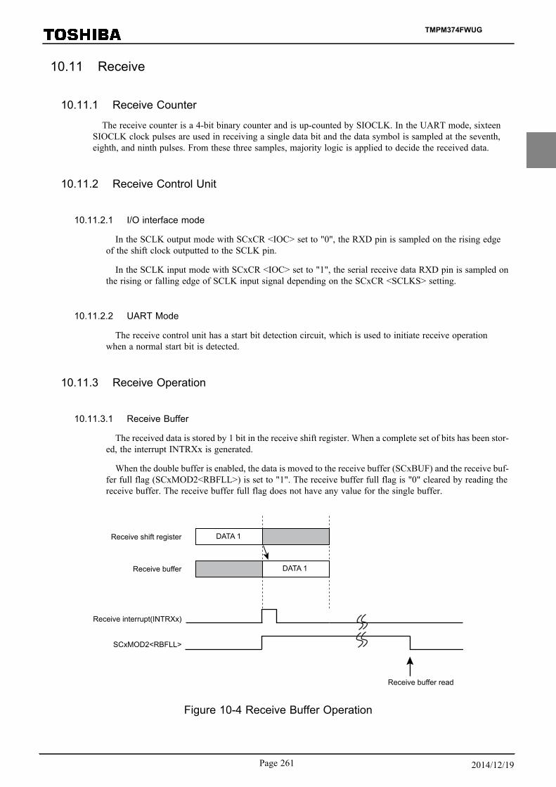
10.11 Receive
10.11.1 Receive Counter
The receive counter is a 4-bit binary counter and is up-counted by SIOCLK. In the UART mode, sixteenSIOCLK clock pulses are used in receiving a single data bit and the data symbol is sampled at the seventh,eighth, and ninth pulses. From these three samples, majority logic is applied to decide the received data.
10.11.2 Receive Control Unit
10.11.2.1 I/O interface mode
In the SCLK output mode with SCxCR <IOC> set to "0", the RXD pin is sampled on the rising edgeof the shift clock outputted to the SCLK pin.
In the SCLK input mode with SCxCR <IOC> set to "1", the serial receive data RXD pin is sampled onthe rising or falling edge of SCLK input signal depending on the SCxCR <SCLKS> setting.
10.11.2.2 UART Mode
The receive control unit has a start bit detection circuit, which is used to initiate receive operationwhen a normal start bit is detected.
10.11.3 Receive Operation
10.11.3.1 Receive Buffer
The received data is stored by 1 bit in the receive shift register. When a complete set of bits has been stor-ed, the interrupt INTRXx is generated.
When the double buffer is enabled, the data is moved to the receive buffer (SCxBUF) and the receive buf-fer full flag (SCxMOD2<RBFLL>) is set to "1". The receive buffer full flag is "0" cleared by reading thereceive buffer. The receive buffer full flag does not have any value for the single buffer.
DATA 1
DATA 1
Receive shift register
Receive buffer
SCxMOD2<RBFLL>
Receive interrupt(INTRXx)
Receive buffer read
Figure 10-4 Receive Buffer Operation
TMPM374FWUG
Page 261 2014/12/19

10.11.3.2 Receive FIFO Operation
When FIFO is enabled, the received data is moved from receive buffer to receive FIFO and the receivebuffer full flag is cleared immediately. An interrupt will be generated according to the SCxRFC<RIL> set-ting.
Note:When the data with parity bit are received in UART mode by using the FIFO, the parity error flag isshown the occurring the parity error in the received data.
The following describes configurations and operations in the half duplex RX mode.
SCxMOD1[6:5] =01 : Transfer mode is set to half duplex mode
SCxFCNF[4:0] = 10111 : Automatically inhibits continuous reception after reaching the fill level.
: The number of bytes to be used in the receive FIFO is the same as the interrupt generation fill lev-el.
SCxRFC[1:0] = 00 : The fill level of FIFO in which generated receive interrupt is set to 4-byte.
SCxRFC[7:6] = 11 : Clears receive FIFO and sets the condition of interrupt generation.
After setting of the above FIFO configuration, the data reception is started by writing "1" to theSCxMOD0 <RXE>. When the data is stored all in the receive shift register, receive buffer and receiveFIFO, SCxMOD0<RXE> is automatically cleared and the receive operation is finished.
In this above condition, if the continuous reception after reaching the fill level is enabled, and it is possi-ble to receive a data continuously with and reading the data in the FIFO.
Receive shift register
Receive buffer
SCxMOD2<RBFLL>
RX Interrupt (INTRXx)
RX FIFO The first stage
The second stage
The third stage
The fourth stage
SCxMOD0<RXE>
DATA1
DATA1
DATA2
DATA2
DATA1
DATA3
DATA2
DATA1
DATA3
DATA4
DATA2
DATA1
DATA3
DATA4
DATA2
DATA1
DATA3
DATA4
DATA1 DATA2
DATA1
DATA3
DATA2
DATA4
DATA3 DATA4 DATA5
DATA5
DATA5
DATA6
Figure 10-5 Receive FIFO Operation
TMPM374FWUG
10. Serial Channel (SIO/UART)
10.11 Receive
Page 2622014/12/19
10.11.3.3 I/O interface mode with SCLK output
In the I/O interface mode and SCLK output setting, SCLK output stops when all received data is stor-ed in the receive buffer and FIFO. So, in this mode, the overrun error flag has no meaning.
The timing of SCLK output stop and re-output depends on receive buffer and FIFO.
(1) Case of single buffer
Stop SCLK output after receiving a data. In this mode, I/O interface can transfer each data withthe transfer device by hand-shake.
When the data in a buffer is read, SCLK output is restarted.
(2) Case of double buffer
Stop SCLK output after receiving the data into a receive shift register and a receive buffer.
When the data is read, SCLK output is restarted.
(3) Case of FIFO
Stop SCLK output after receiving the data into a shift register, received buffer and FIFO.
When one byte data is read, the data in the received buffer is transferred into FIFO and the datain the receive shift register is transferred into received buffer and SCLK output is restarted.
And if SCxFCNF<RXTXCNT> is set to "1", SCLK stops and receive operation stops with clear-ing SCxMOD0<RXE> bit too.
10.11.3.4 Read Received Data
In spite of enabling or disabling FIFO, read the received data from the receive buffer (SCxBUF).
When receive FIFO is disabled, the buffer full flag SCxMOD2<RBFLL> is cleared to "0" by this read-ing. In the case of the next data can be received in the receive shift register before reading a data fromthe receive buffer. The parity bit to be added in the 8-bit UART mode as well as the most significant bitin the 9-bit UART mode will be stored in SCxCR<RB8>.
When the receive FIFO is available, the 9-bit UART mode is prohibited because up to 8-bit data canbe stored in FIFO. In the 8-bit UART mode, the parity bit is lost but parity error is determined and the re-sult is stored in SCxCR<PERR>.
10.11.3.5 Wake-up Function
In the 9-bit UART mode, the slave controller can be operated in the wake-up mode by setting the wake-up function SCxMOD0 <WU> to "1." In this case, the interrupt INTRXx will be generated only whenSCxCR <RB8> is set to "1."
TMPM374FWUG
Page 263 2014/12/19

10.11.3.6 Overrun Error
When FIFO is disabled, the overrun error is occurred and set overrun flag without completing dataread before receiving the next data. When overrun error is occurred, a content of receive buffer andSCxCR<RB8> is not lost, but a content of receive shift register is lost.
When FIFO is enabled, overrun error is occurred and set overrun flag by no reading the data before mov-ing the next data into received buffer when FIFO is full. In this case, the content of FIFO are not lost.
In the I/O interface mode with SCLK output setting, the clock output automatically stops, so this flaghas no meaning.
Note:When the mode is changed from I/O interface SCLK output mode to the other mode, read SCxCRand clear overrun flag.
TMPM374FWUG
10. Serial Channel (SIO/UART)
10.11 Receive
Page 2642014/12/19
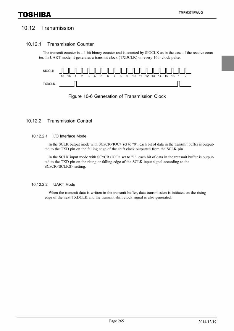
10.12 Transmission
10.12.1 Transmission Counter
The transmit counter is a 4-bit binary counter and is counted by SIOCLK as in the case of the receive coun-ter. In UART mode, it generates a transmit clock (TXDCLK) on every 16th clock pulse.
15 16 1 2 3 4 5 6 7 8 9 10 11 12 13 14 15 16 1 2
SIOCLK
TXDCLK
Figure 10-6 Generation of Transmission Clock
10.12.2 Transmission Control
10.12.2.1 I/O Interface Mode
In the SCLK output mode with SCxCR<IOC> set to "0", each bit of data in the transmit buffer is output-ted to the TXD pin on the falling edge of the shift clock outputted from the SCLK pin.
In the SCLK input mode with SCxCR<IOC> set to "1", each bit of data in the transmit buffer is output-ted to the TXD pin on the rising or falling edge of the SCLK input signal according to theSCxCR<SCLKS> setting.
10.12.2.2 UART Mode
When the transmit data is written in the transmit buffer, data transmission is initiated on the risingedge of the next TXDCLK and the transmit shift clock signal is also generated.
TMPM374FWUG
Page 265 2014/12/19
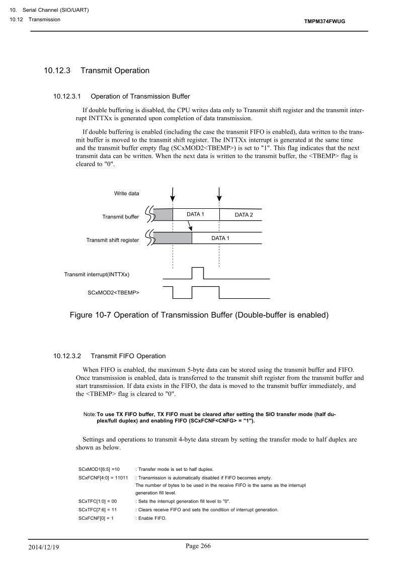
10.12.3 Transmit Operation
10.12.3.1 Operation of Transmission Buffer
If double buffering is disabled, the CPU writes data only to Transmit shift register and the transmit inter-rupt INTTXx is generated upon completion of data transmission.
If double buffering is enabled (including the case the transmit FIFO is enabled), data written to the trans-mit buffer is moved to the transmit shift register. The INTTXx interrupt is generated at the same timeand the transmit buffer empty flag (SCxMOD2<TBEMP>) is set to "1". This flag indicates that the nexttransmit data can be written. When the next data is written to the transmit buffer, the <TBEMP> flag iscleared to "0".
DATA 1 Transmit buffer
SCxMOD2<TBEMP>
Transmit interrupt(INTTXx)
Write data
DATA 2
DATA 1 Transmit shift register
Figure 10-7 Operation of Transmission Buffer (Double-buffer is enabled)
10.12.3.2 Transmit FIFO Operation
When FIFO is enabled, the maximum 5-byte data can be stored using the transmit buffer and FIFO.Once transmission is enabled, data is transferred to the transmit shift register from the transmit buffer andstart transmission. If data exists in the FIFO, the data is moved to the transmit buffer immediately, andthe <TBEMP> flag is cleared to "0".
Note:To use TX FIFO buffer, TX FIFO must be cleared after setting the SIO transfer mode (half du-plex/full duplex) and enabling FIFO (SCxFCNF<CNFG> = "1").
Settings and operations to transmit 4-byte data stream by setting the transfer mode to half duplex areshown as below.
SCxMOD1[6:5] =10 : Transfer mode is set to half duplex.
SCxFCNF[4:0] = 11011 : Transmission is automatically disabled if FIFO becomes empty.The number of bytes to be used in the receive FIFO is the same as the interruptgeneration fill level.
SCxTFC[1:0] = 00 : Sets the interrupt generation fill level to "0".
SCxTFC[7:6] = 11 : Clears receive FIFO and sets the condition of interrupt generation.
SCxFCNF[0] = 1 : Enable FIFO.
TMPM374FWUG
10. Serial Channel (SIO/UART)
10.12 Transmission
Page 2662014/12/19

After above settings are configured, data transmission can be initiated by writing 5 bytes of data to thetransmit buffer and FIFO, and setting the SCxMOD1<TXE> bit to "1". When the last transmit data ismoved to the transmit buffer, the transmit FIFO interrupt is generated. When transmission of the last datais completed, the transmission sequence is terminated.
Once above settings are configured, if the transmission is not set as auto disabled, the transmissionshould lasts by writing transmit data.
Transmit FIFO fourth stage
SCxMOD2<TBEMP>
DATA 5
Transmit buffer
Transmit shift register
Transmit interrupt(INTTXx)
SCxMOD1<TXE>
Third stage
Second stage
First stage
DATA 4
DATA 3
DATA 2
DATA 1
DATA 5
DATA 4
DATA 3
DATA 2
DATA 5
DATA 4
DATA 3
DATA 1 DATA 2 DATA 3
DATA 5
DATA 4 DATA 5
DATA 4 DATA 5
TMPM374FWUG
Page 267 2014/12/19
10.12.3.3 I/O interface Mode/Transmission by SCLK Output
If SCLK is set to generate clock the I/O interface mode, the SCLK output automatically stops when alldata transmission is completed and underrun error will not occur.
The timing of suspension and resume of SCLK output is different depending on the buffer and FIFO us-age.
(1) Single Buffer
The SCLK output stops each time one frame of data is transferred. Handshaking for each datawith the other side of communication can be enabled. The SCLK output resumes when the next da-ta is written in the buffer.
(2) Double Buffer
The SCLK output stops upon completion of data transmission of the transmit shift register andthe transmit buffer. The SCLK output resumes when the next data is written in the buffer.
(3) FIFO
The transmission of all data stored in the transmit shift register, transmit buffer and FIFO is comple-ted, the SCLK output stops. The next data is written, SCLK output resumes.
If SCxFCNF<RXTXCNT> is configured, SCxMOD0<TXE> bit is cleared at the same time asSCLK stop and the transmission stops.
10.12.3.4 Under-run error
If the transmit FIFO is disabled in the I/O interface SCLK input mode and if no data is set in transmit buf-fer before the next frame clock input, which occurs upon completion of data transmission from transmitshift register, an under-run error occurs and SCxCR<PERR> is set to "1".
In the I/O interface mode with SCLK output setting, the clock output automatically stops, so this flaghas no meaning.
Note:Before switching the I/O interface SCLK output mode to other modes, read the SCxCR regis-ter and clear the underrun flag.
TMPM374FWUG
10. Serial Channel (SIO/UART)
10.12 Transmission
Page 2682014/12/19

10.13 Handshake functionThe function of the handshake is to enable frame-by-frame data transmission by using the CTS (Clear to send)
pin and to prevent overrun errors. This function can be enabled or disabled by SCxMOD0<CTSE>.
When the CTS pin is set to "High" level, the current data transmission can be completed but the next data trans-mission is suspended until the CTS pin returns to the "Low" level. However in this case, the INTTXx interrupt is gen-erated in the normal timing, the next transmit data is written in the transmit buffer, and it waits until it is ready totransmit data.
Note 1: If the CTS signal is set to "H" during transmission, the next data transmission is suspended after the currenttransmission is completed.(Point "a" in Figure 10-9)
Note 2: Data transmission starts on the first falling edge of the TXDCLK clock after CTS is set to "L".(Point "b"in Figure 10-9)
Although no RTS pin is provided, a handshake control function can easily implemented by assigning one bit ofthe port for the RTS function. By setting the port to "High" level upon completion of data reception (in the re-ceive interrupt routine), the transmit side can be requested to suspend data transmission.
TXD
CTS
RXD
RTS (Any port)
Transmit side Receive side
Figure 10-8 Handshake Function
Transmission issuspended duringthis period.
Start bit Bit 0TXD
SIOCLK
Data write to transmit buffer or shift register
TXDCLK
CTS
13 14 15 16 1 2 3 14 15 16 1 2 3ab
Figure 10-9 CTS Signal timing
TMPM374FWUG
Page 269 2014/12/19

10.14 Interrupt/Error Generation Timing
10.14.1 RX Interrupts
Figure 10-10 shows the data flow of receive operation and the route of read.
Figure 10-10 Receive Buffer/FIFO Configuration Diagram
10.14.1.1 Single Buffer / Double Buffer
RX interrupts are generated at the time depends on the transfer mode and the buffer configurations,which are given as follows.
Buffer
ConfigurationsUART modes IO interface modes
Single Buffer −Immediately after the rising / falling edge of the last SCLK(Rising or falling is determined according to SCxCR<SCLKS> setting.)
Double Buffer Around the center of the first stop bitImmediately after the rising / falling edge of the last SCLK(Rising or falling is determined according to SCxCR<SCLKS> setting.)On data transfer from the shift register to the buffer by reading buffer.
Note:Interrupts are not generated when an overrun error is occurred.
10.14.1.2 FIFO
In use of FIFO, receive interrupt is generated on the condition that the following either operation andSCxRFC<RFIS > setting are established.
・ Reception completion of all bits of one frame.・ Reading FIFO
Interrupt conditions are decided by the SCxRFC<RFIS> settings as described in Table 10-11.
Table 10-11 Receive Interrupt conditions in use of FIFO
SCxRFC<RFIS> Interrupt conditions
"0" "The fill level of FIFO" is equal to "the fill level of FIFO interruption generation."
"1" "The fill level of FIFO" is greater than or equal to "the fill level of FIFO intrruption generation."
TMPM374FWUG
10. Serial Channel (SIO/UART)
10.14 Interrupt/Error Generation Timing
Page 2702014/12/19
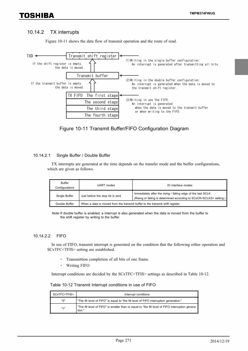
10.14.2 TX interrupts
Figure 10-11 shows the data flow of transmit operation and the route of read.
Figure 10-11 Transmit Buffer/FIFO Configuration Diagram
10.14.2.1 Single Buffer / Double Buffer
TX interrupts are generated at the time depends on the transfer mode and the buffer configurations,which are given as follows.
Buffer
ConfigurationsUART modes IO interface modes
Single Buffer Just before the stop bit is sentImmediately after the rising / falling edge of the last SCLK(Rising or falling is determined according to SCxCR<SCLKS> setting.)
Double Buffer When a data is moved from the transmit buffet to the transmit shift register.
Note:If double buffer is enabled, a interrupt is also generated when the data is moved from the buffer tothe shift register by writing to the buffer.
10.14.2.2 FIFO
In use of FIFO, transmit interrupt is generated on the condition that the following either operation andSCxTFC<TFIS> setting are established.
・ Transmittion completion of all bits of one frame.・ Writing FIFO
Interrupt conditions are decided by the SCxTFC<TFIS> settings as described in Table 10-12.
Table 10-12 Transmit Interrupt conditions in use of FIFO
SCxTFC<TFIS> Interrupt conditions
"0" "The fill level of FIFO" is equal to "the fill level of FIFO interruption generation."
"1" "The fill level of FIFO" is smaller than or equal to "the fill level of FIFO interruption genera-tion."
TMPM374FWUG
Page 271 2014/12/19
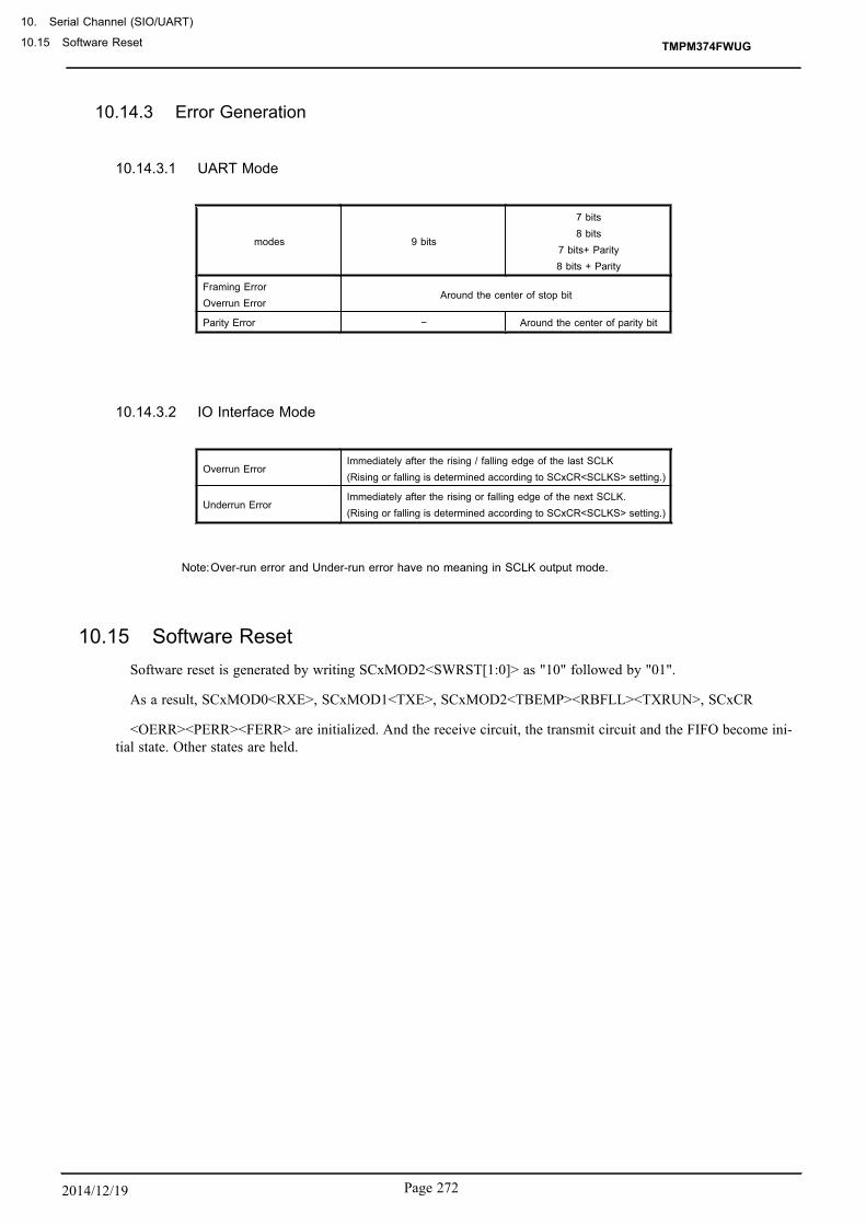
10.14.3 Error Generation
10.14.3.1 UART Mode
modes 9 bits
7 bits8 bits
7 bits+ Parity8 bits + Parity
Framing ErrorOverrun Error
Around the center of stop bit
Parity Error − Around the center of parity bit
10.14.3.2 IO Interface Mode
Overrun ErrorImmediately after the rising / falling edge of the last SCLK(Rising or falling is determined according to SCxCR<SCLKS> setting.)
Underrun ErrorImmediately after the rising or falling edge of the next SCLK.(Rising or falling is determined according to SCxCR<SCLKS> setting.)
Note:Over-run error and Under-run error have no meaning in SCLK output mode.
10.15 Software ResetSoftware reset is generated by writing SCxMOD2<SWRST[1:0]> as "10" followed by "01".
As a result, SCxMOD0<RXE>, SCxMOD1<TXE>, SCxMOD2<TBEMP><RBFLL><TXRUN>, SCxCR
<OERR><PERR><FERR> are initialized. And the receive circuit, the transmit circuit and the FIFO become ini-tial state. Other states are held.
TMPM374FWUG
10. Serial Channel (SIO/UART)
10.15 Software Reset
Page 2722014/12/19
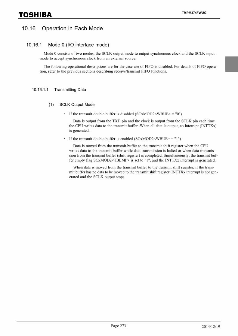
10.16 Operation in Each Mode
10.16.1 Mode 0 (I/O interface mode)
Mode 0 consists of two modes, the SCLK output mode to output synchronous clock and the SCLK inputmode to accept synchronous clock from an external source.
The following operational descriptions are for the case use of FIFO is disabled. For details of FIFO opera-tion, refer to the previous sections describing receive/transmit FIFO functions.
10.16.1.1 Transmitting Data
(1) SCLK Output Mode
・ If the transmit double buffer is disabled (SCxMOD2<WBUF> = "0")
Data is output from the TXD pin and the clock is output from the SCLK pin each timethe CPU writes data to the transmit buffer. When all data is output, an interrupt (INTTXx)is generated.
・ If the transmit double buffer is enabled (SCxMOD2<WBUF> = "1")
Data is moved from the transmit buffer to the transmit shift register when the CPUwrites data to the transmit buffer while data transmission is halted or when data transmis-sion from the transmit buffer (shift register) is completed. Simultaneously, the transmit buf-fer empty flag SCxMOD2<TBEMP> is set to "1", and the INTTXx interrupt is generated.
When data is moved from the transmit buffer to the transmit shift register, if the trans-mit buffer has no data to be moved to the transmit shift register, INTTXx interrupt is not gen-erated and the SCLK output stops.
TMPM374FWUG
Page 273 2014/12/19

bit 0 bit 1 bit 6TXD
(INTTXx interrupt request)
Transmit data write timing
SCLK output
bit 7 bit 0
<WBUF> = "0" (if double buffering is disabled)
bit 0 bit 1 bit 6TXD
(INTTXx interrupt request)
SCLK output
<WBUF> = "1" (if double buffering is enabled and there is data in buffer)
bit 7 bit 0
TBEMP
bit 0 bit 1 bit 6TXD
(INTTXx interrupt request)
Transmit data write timing
SCLK output
<WBUF> = "1" (if double buffering is enabled and threre is no data in buffer)
bit 7
TBEMP
Transmit datawrite timing
Figure 10-12 Transmit Operation in the I/O Interface Mode (SCLK Output Mode)
TMPM374FWUG
10. Serial Channel (SIO/UART)
10.16 Operation in Each Mode
Page 2742014/12/19
(2) SCLK Input Mode
・ If double buffering is disabled (SCxMOD2<WBUF> = "0")
If the SCLK is input in the condition where data is written in the transmit buffer, 8-bit da-ta is outputted from the TXD pin. When all data is output, an interrupt INTTXx is gener-ated. The next transmit data must be written before the timing point "A" as shown in Fig-ure 10-13.
・ If double buffer is enabled (SCxMOD2<WBUF> = "1")
Data is moved from the transmit buffer to the transmit shift register when the CPUwrites data to the transmit buffer before the SCLK input becomes active or when data trans-mission from the transmit shift register is completed. Simultaneously, the transmit bufferempty flag SCxMOD2<TBEMP> is set to "1", and the INTTXx interrupt is generated.
If the SCLK input becomes active while no data is in the transmit buffer, although the in-ternal bit counter is started, an under-run error occurs and 8-bit dummy data (0xFF) is sent.
TMPM374FWUG
Page 275 2014/12/19
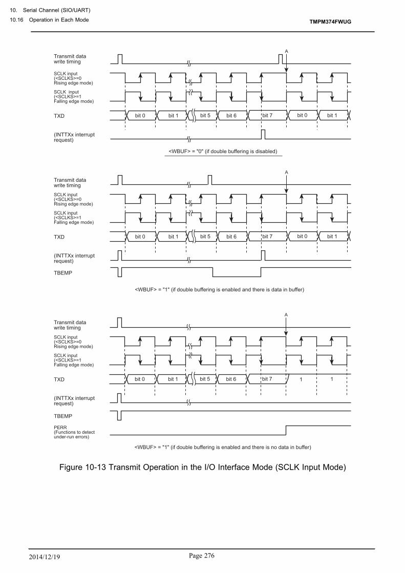
bit 0 bit 1 bit 6TXD
(INTTXx interrupt request)
Transmit data write timing
SCLK input(<SCLKS>=1Falling edge mode)
SCLK input(<SCLKS>=0Rising edge mode)
bit 5 bit 7 bit 1bit 0
A
<WBUF> = "0" (if double buffering is disabled)
bit 0 bit 1 bit 6TXD
(INTTXx interrupt request)
SCLK input(<SCLKS>=1Falling edge mode)
SCLK input(<SCLKS>=0Rising edge mode)
bit 5 bit 7 bit 1bit 0
A
<WBUF> = "1" (if double buffering is enabled and there is data in buffer)
TBEMP
bit 0 bit 1 bit 6TXD
(INTTXx interrupt request)
SCLK input (<SCLKS>=1Falling edge mode)
SCLK input(<SCLKS>=0Rising edge mode)
bit 5 bit 7
A
<WBUF> = "1" (if double buffering is enabled and there is no data in buffer)
TBEMP
1 1
PERR (Functions to detect under-run errors)
Transmit data write timing
Transmit data write timing
Figure 10-13 Transmit Operation in the I/O Interface Mode (SCLK Input Mode)
TMPM374FWUG
10. Serial Channel (SIO/UART)
10.16 Operation in Each Mode
Page 2762014/12/19

10.16.1.2 Receive
(1) SCLK Output Mode
The SCLK output can be started by setting the receive enable bit SCxMOD0<RXE> to "1".
・ If double buffer is disabled (SCxMOD2<WBUF> = "0")
A clock pulse is outputted from the SCLK pin and the next data is stored into the shift reg-ister each time the CPU reads received data. When all the 8 bits are received, the INTRXxinterrupt is generated.
・ If double buffer is enabled (SCxMOD2<WBUF> = "1")
Data stored in the shift register is moved to the receive buffer and the receive buffer canreceive the next frame. A data is moved from the shift register to the receive buffer, the re-ceive buffer full flag SCxMOD2<RBFLL> is set to "1" and the INTRXx is generated.
While data is in the receive buffer, if the data cannot be read from the receive buffer be-fore completing reception of the next 8 bits, the INTRXx interrupt is not generated and theSCLK output stops. In this state, reading data from the receive buffer allows data in theshift register to move to the receive buffer and thus the INTRXx interrupt is generated anddata reception resumes.
TMPM374FWUG
Page 277 2014/12/19

bit 0 bit 1 bit 6RXD
(INTRX interrupt request)
SCLK output
bit 7 bit 0
<WBUF> = "0" (if double buffering is disable
bit 0 bit 1 bit 6RXD
(INTRX interrupt request)
SCLK output
bit 0
<WBUF> = "1" (if double buffering is enabled and data is read from buffer)
bit 7bit 7
RBFLL
bit 0 bit 1 bit 6RXD
(INTRX interrupt request)
SCLK output
<WBUF> = "1" (if double buffering is enabled and data cannot be read from buffer)
bit 7bit 7
RBFLL
Figure 10-14 Receive Operation in the I/O Interface Mode (SCLK Output Mode)
TMPM374FWUG
10. Serial Channel (SIO/UART)
10.16 Operation in Each Mode
Page 2782014/12/19

(2) SCLK Input Mode
In the SCLK input mode, receiving double buffering is always enabled, the received frame canbe moved to the receive buffer from the shift register, and the receive buffer can receive the nextframe successively.
The INTRXx receive interrupt is generated each time received data is moved to the receive buffer.
bit 0 bit 1 bit 6RXD
(INTRXx interrupt request)
Receive data read timing
SCLK input(<SCLKS>=”1”Falling mode)
SCLK input(<SCLKS>=”0”Rising mode)
bit 5 bit 7 bit 0
If data is read from buffer
RBFLL
bit 0 bit 1 bit 6RXD
(INTRXx interrupt request)
Receive data read timing
SCLK input(<SCLKS>=”1”Falling mode)
SCLK input(<SCLKS>=”0”Rising mode)
bit 5 bit 7 bit 0
If data cannot be read from buffer
RBFLL
OERR
Figure 10-15 Receive Operation in the I/O Interface Mode (SCLK Input Mode)
TMPM374FWUG
Page 279 2014/12/19

10.16.1.3 Transmit and Receive (Full-duplex)
(1) SCLK Output Mode
・ If SCxMOD2<WBUF> is set to "0" and the double buffers are disabled
SCLK is outputted when the CPU writes data to the transmit buffer.
Subsequently, 8 bits of data are shifted into receive shift register and the INTRXx re-ceive interrupt is generated. Concurrently, 8 bits of data written to the transmit buffer are out-putted from the TXD pin, the INTTXx transmit interrupt is generated when transmissionof all data bits has been completed. Then, the SCLK output stops.
The next round of data transmission and reception starts when the data is read from the re-ceive buffer and the next transmit data is written to the transmit buffer by the CPU. The or-der of reading the receive buffer and writing to the transmit buffer can be freely deter-mined. Data transmission is resumed only when both conditions are satisfied.
・ If SCxMOD2<WBUF> is set to "1" and the double buffers are enabled
SCLK is outputted when the CPU writes data to the transmit buffer.
8 bits of data are shifted into the receive shift register, moved to the receive buffer, andthe INTRXx interrupt is generated. While 8 bits of data is received, 8 bits of transmit datais outputted from the TXD pin. When all data bits are sent out, the INTTXx interrupt is gen-erated and the next data is moved from the transmit buffer to the transmit shift register.
If the transmit buffer has no data to be moved to the transmit buffer(SCxMOD2<TBEMP> = 1) or when the receive buffer is full (SCxMOD2<RBFULL> =1), the SCLK output is stopped. When both conditions, receive data is read and transmit da-ta is written, are satisfied, the SCLK output is resumed and the next round of data transmis-sion and reception is started.
TMPM374FWUG
10. Serial Channel (SIO/UART)
10.16 Operation in Each Mode
Page 2802014/12/19

bit 0 bit 1 bit 6TXD
(INTTXx interrupt request)
Transmit datawrite timing
SCLK output
bit 5 bit 7 bit 1bit 0
<WBUF> = "0" (if double buffering is disabled)
Receive dataread timing
bit 0 bit 1 bit 6RXD bit 5 bit 7 bit 1bit 0
(INTRXx interrupt request)
bit 0 bit 1 bit 6TXD
(INTTXx interrupt request)
Transmit datawrite timing
SCLK output
bit 5 bit 7 bit 1bit 0
<WBUF> = "1" (if double buffering is enabled)
Receive dataread timing
bit 0 bit 1 bit 6RXD bit 5 bit 7 bit 1bit 0
(INTRXx interrupt request)
bit 0 bit 1 bit 6TXD
(INTTXx interrupt request)
Transmit datawrite timing
SCLK output
bit 5 bit 7
<WBUF> = "1" (if double buffering is enabled)
Receive dataread timing
bit 0 bit 1 bit 6RXD bit 5 bit 7
(INTRXx interrupt request)
Figure 10-16 Transmit/Receive Operation in the I/O Interface Mode (SCLK Output Mode)
TMPM374FWUG
Page 281 2014/12/19

(2) SCLK Input Mode
・ If SCxMOD2<WBUF> is set to "0" and the transmit double buffer is disabled
When receiving data, double buffer is always enabled regardless of the SCxMOD2<WBUF> settings.
8-bit data written in the transmit buffer is outputted from the TXD pin and 8 bit of datais shifted into the receive buffer when the SCLK input becomes active.The INTTXx inter-rupt is generated upon completion of data transmission. The INTRXx interrupt is gener-ated when the data is moved from receive shift register to receive buffer after completionof data reception.
Note that transmit data must be written into the transmit buffer before the SCLK inputfor the next frame (data must be written before the point A in Figure 10-17). Data must beread before completing reception of the next frame data.
・ If SCxMOD2<WBUF> is set to "1" and the double buffer is enabled.
The interrupt INTTXx is generated at the timing the transmit buffer data is moved to thetransmit shift register after completing data transmission from the transmit shift register.At the same time, data received is shifted to the shift register, it is moved to the receive buf-fer, and the INTRXx interrupt is generated.
Note that transmit data must be written into the transmit buffer before the SCLK inputfor the next frame (data must be written before the point A in Figure 10-17). Data must beread before completing reception of the next frame data.
Upon the SCLK input for the next frame, transmission from transmit shift register (inwhich data has been moved from transmit buffer) is started while receive data is shifted in-to receive shift register simultaneously.
If data in receive buffer has not been read when the last bit of the frame is received, an over-run error occurs. Similarly, if there is no data written to transmit buffer when SCLK forthe next frame is input, an under-run error occurs.
TMPM374FWUG
10. Serial Channel (SIO/UART)
10.16 Operation in Each Mode
Page 2822014/12/19

bit 0 bit 1 bit 6TXD
(INTTXx interrupt request)
Transmit data write timing
SCLK input
bit 5 bit 7 bit 1bit 0
A
<WBUF> = "0" (if double buffering is disabled)
Receive dataread timing
bit 0 bit 1 bit 6RXD bit 5 bit 7 bit 1bit 0
(INTRXx interrupt request)
bit 0 bit 1 bit 6TXD
(INTTXx interrupt request)
Transmit data write timing
SCLK input
bit 5 bit 7 bit 1bit 0
<WBUF> = "1" (if double buffering is enabled with no errors)
Receive dataread timing
bit 0 bit 1 bit 6RXD bit 5 bit 7 bit 1bit 0
(INTRXx interrupt request)
bit 0 bit 1 bit 6TXD
(INTTXx interrupt request)
Transmit data write timing
SCLK input
bit 5 bit 7 bit 1bit 0
<WBUF> = "1" (if double buffering is enabled with error generation)
Receive dataread timing
bit 0 bit 1 bit 6RXD bit 5 bit 7 bit 1bit 0
(INTRXx interrupt request)
PERR(Under-run errors)
A
A
Figure 10-17 Transmit/Receive Operation in the I/O Interface Mode (SCLK Input Mode)
TMPM374FWUG
Page 283 2014/12/19
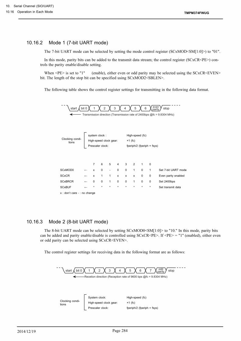
10.16.2 Mode 1 (7-bit UART mode)
The 7-bit UART mode can be selected by setting the mode control register (SCxMOD<SM[1:0]>) to "01".
In this mode, parity bits can be added to the transmit data stream; the control register (SCxCR<PE>) con-trols the parity enable/disable setting.
When <PE> is set to "1" (enable), either even or odd parity may be selected using the SCxCR<EVEN>bit. The length of the stop bit can be specified using SCxMOD2<SBLEN>.
The following table shows the control register settings for transmitting in the following data format.
stopstart bit 0 1 2 3 4 5 6 evenparity
Transmission direction (Transmission rate of 2400bps @fc = 9.8304 MHz)
Clocking condi-tions
system clock : High-speed (fc)
High-speed clock gear: ×1 (fc)
Prescaler clock: fperiph/2 (fperiph = fsys)
7 6 5 4 3 2 1 0
SCxMOD0 ← x 0 - 0 0 1 0 1 Set 7-bit UART mode
SCxCR ← x 1 1 x x x 0 0 Even parity enabled
SCxBRCR ← 0 0 1 0 0 1 0 0 Set 2400bps
SCxBUF ← * * * * * * * * Set transmit data
x : don’t care - : no change
10.16.3 Mode 2 (8-bit UART mode)
The 8-bit UART mode can be selected by setting SCxMOD0<SM[1:0]> to "10." In this mode, parity bitscan be added and parity enable/disable is controlled using SCxCR<PE>. If <PE> = "1" (enabled), either evenor odd parity can be selected using SCxCR<EVEN>.
The control register settings for receiving data in the following format are as follows:
stop start bit 0 1 2 3 4 5 6 7 odd parity
Recetion direction (Reception rate of 9600 bps @fc = 9.8304 MHz)
Clocking condi-tions
System clock: High-speed (fc)
High-speed clock gear: ×1 (fc)
Prescaler clock: fperiph/2 (fperiph = fsys)
TMPM374FWUG
10. Serial Channel (SIO/UART)
10.16 Operation in Each Mode
Page 2842014/12/19

7 6 5 4 3 2 1 0
SCxMOD0 ← x 0 0 0 1 0 0 1 Set 8-bit UART mode
SCxCR ← x 0 1 x x x 0 0 Odd parity enabled
SCxBRCR ← 0 0 0 1 0 1 0 0 Set 9600bps
SCxMOD0 ← - - 1 - - - - - Reception enabled
x : don’t care - : no change
10.16.4 Mode 3 (9-bit UART mode)
The 9-bit UART mode can be selected by setting SCxMOD0<SM[1:0]> to "11." In this mode, parity bitsmust be disabled (SCxCR<PE> = "0").
The most significant bit (9th bit) is written to SCxMOD0<TB8> for transmitting data. The data is storedin SCxCR<RB8>.
When writing or reading data to/from the buffers, the most significant bit must be written or read first be-fore writing or reading to/from SCxBUF.
The stop bit length can be specified using SCxMOD2<SBLEN>.
10.16.4.1 Wake up function
In the 9-bit UART mode, slave controllers can be operated in the wake-up mode by setting the wake-up function control bit SCxMOD0<WU> to "1."
In this case, the interrupt INTRXx will be generated only when SCxCR<RB8> is set to "1".
Note:The TXD pin of the slave controller must be set to the open drain output mode using the PxOD reg-ister.
TXD RXD
Master
TXD RXD
Slave1
TXD RXD
Slave2
TXD RXD
Slave3
Figure 10-18 Serial Links to Use Wake-up Function
TMPM374FWUG
Page 285 2014/12/19

10.16.4.2 Protocol
1. Select the 9-bit UART mode for the master and slave controllers.
2. Set SCxMOD0<WU> to "1" for the slave controllers to make them ready to receive data.
3. The master controller is to transmit a single frame of data that includes the slave controller se-lect code (8 bits). In this, the most significant bit (bit 8) <TB8> must be set to "1".
stopstart bit 0 1 2 3 4 5 6 7 8
Select code of the slave controller "1"
4. Each slave controller receives the above data frame; if the code received matches with the con-troller's own select code, it clears the WU bit to "0".
5. The master controller transmits data to the designated slave controller (the controller of whichSCxMOD<WU> bit is cleared to "0"). In this, the most significant bit (bit 8) <TB8> must beset to "0".
stopstart bit 0 1 2 3 4 5 6 7 bit 8
Data "0"
6. The slave controllers with the <WU> bit set to "1" ignore the receive data because the most sig-nificant bit (bit 8) <RB8> is set to "0" and thus no interrupt (INTRXx) is generated.Also, theslave controller with the <WU> bit set to "0" can transmit data to the master controller to in-form that the data has been successfully received.
TMPM374FWUG
10. Serial Channel (SIO/UART)
10.16 Operation in Each Mode
Page 2862014/12/19
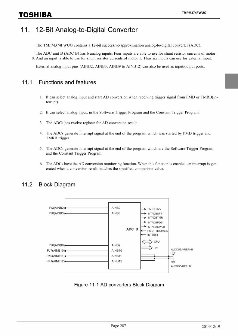
11. 12-Bit Analog-to-Digital Converter
The TMPM374FWUG contains a 12-bit successive-approximation analog-to-digital converter (ADC).
The ADC unit B (ADC B) has 6 analog inputs. Four inputs are able to use for shunt resistor currents of motor0. And an input is able to use for shunt resistor currents of motor 1. Thus six inputs can use for external input.
External analog input pins (AINB2, AINB3, AINB9 to AINB12) can also be used as input/output ports.
11.1 Functions and features
1. It can select analog input and start AD conversion when receiving trigger signal from PMD or TMRB(in-terrupt).
2. It can select analog input, in the Software Trigger Program and the Constant Trigger Program.
3. The ADCs has twelve register for AD conversion result.
4. The ADCs generate interrupt signal at the end of the program which was started by PMD trigger andTMRB trigger.
5. The ADCs generate interrupt signal at the end of the program which are the Software Trigger Programand the Constant Trigger Program.
6. The ADCs have the AD conversion monitoring function. When this function is enabled, an interrupt is gen-erated when a conversion result matches the specified comparison value.
11.2 Block Diagram
AINB2
AINB3
ADC B
PI3(AINB2)
AVDD5B/VREFHB
AVSSB/VREFLB
CPU
VE
INTADBPDB
PMD1 OVV
INTADBSFTINTADBTMR
INTADBCPA/B
PJ0(AINB3)
AINB9
AINB10
AINB11
AINB12
PJ6(AINB9)
PJ7(AINB10)
PK0(AINB11)
PK1(AINB12)
PMD1 TRG0 to 5INTTB51
Figure 11-1 AD converters Block Diagram
TMPM374FWUG
Page 287 2014/12/19
11.3 List of Registers
Unit Base Address
Unit B 0x4003_0200
Register Name Address(Base+)
Clock Setting Register ADBCLK 0x0000
Mode Setting Register 0 ADBMOD0 0x0004
Mode Setting Register 1 ADBMOD1 0x0008
Mode Setting Register 2 ADBMOD2 0x000C
Monitoring Setting Register 0 ADBCMPCR0 0x0010
Monitoring Setting Register 1 ADBCMPCR1 0x0014
Conversion Result Compare Register 0 ADBCMP0 0x0018
Conversion Result Compare Register 1 ADBCMP1 0x001C
Conversion Result Register 0 ADBREG0 0x0020
Conversion Result Register 1 ADBREG1 0x0024
Conversion Result Register 2 ADBREG2 0x0028
Conversion Result Register 3 ADBREG3 0x002C
Conversion Result Register 4 ADBREG4 0x0030
Conversion Result Register 5 ADBREG5 0x0034
Conversion Result Register 6 ADBREG6 0x0038
Conversion Result Register 7 ADBREG7 0x003C
Conversion Result Register 8 ADBREG8 0x0040
Conversion Result Register 9 ADBREG9 0x0044
Conversion Result Register 10 ADBREG10 0x0048
Conversion Result Register 11 ADBREG11 0x004C
Reserved - 0x0050
Reserved - 0x0054
Reserved - 0x0058
Reserved - 0x005C
Reserved - 0x0060
Reserved - 0x0064
PMD Trigger Program Number Select Register 6 ADBPSEL6 0x0068
PMD Trigger Program Number Select Register 7 ADBPSEL7 0x006C
PMD Trigger Program Number Select Register 8 ADBPSEL8 0x0070
PMD Trigger Program Number Select Register 9 ADBPSEL9 0x0074
PMD Trigger Program Number Select Register 10 ADBPSEL10 0x0078
PMD Trigger Program Number Select Register 11 ADBPSEL11 0x007C
PMD Trigger Interrupt Select Register 0 ADBPINTS0 0x0080
PMD Trigger Interrupt Select Register 1 ADBPINTS1 0x0084
PMD Trigger Interrupt Select Register 2 ADBPINTS2 0x0088
PMD Trigger Interrupt Select Register 3 ADBPINTS3 0x008C
PMD Trigger Interrupt Select Register 4 ADBPINTS4 0x0090
PMD Trigger Interrupt Select Register 5 ADBPINTS5 0x0094
PMD Trigger Program Register 0 ADBPSET0 0x0098
PMD Trigger Program Register 1 ADBPSET1 0x009C
PMD Trigger Program Register 2 ADBPSET2 0x00A0
PMD Trigger Program Register 3 ADBPSET3 0x00A4
PMD Trigger Program Register 4 ADBPSET4 0x00A8
PMD Trigger Program Register 5 ADBPSET5 0x00AC
TMPM374FWUG
11. 12-Bit Analog-to-Digital Converter
11.3 List of Registers
Page 2882014/12/19

Register Name Address(Base+)
Timer Trigger Program Registers 0 to 3 ADBTSET03 0x00B0
Timer Trigger Program Registers 4 to 7 ADBTSET47 0x00B4
Timer Trigger Program Registers 8 to 11 ADBTSET811 0x00B8
Software Trigger Program Registers 0 to 3 ADBSSET03 0x00BC
Software Trigger Program Registers 4 to 7 ADBSSET47 0x00C0
Software Trigger Program Registers 8 to 11 ADBSSET811 0x00C4
Constant Conversion Program Registers0 to 3 ADBASET03 0x00C8
Constant Conversion Program Registers 4 to 7 ADBASET47 0x00CC
Constant Conversion Program Registers 8 to 11 ADBASET811 0x00D0
Reserved - 0x00D4
Note:Access to the "Reserved" areas are prohibited.
TMPM374FWUG
Page 289 2014/12/19

11.4 Register DescriptionsAD conversion is performed at the clock frequency selected in the ADC Clock Setting Register.
11.4.1 ADBCLK (Clock Setting Register)
31 30 29 28 27 26 25 24
bit symbol - - - - - - - -
After reset 0 0 0 0 0 0 0 0
23 22 21 20 19 18 17 16
bit symbol - - - - - - - -
After reset 0 0 0 0 0 0 0 0
15 14 13 12 11 10 9 8
bit symbol - - - - - - - -
After reset 0 0 0 0 0 0 0 0
7 6 5 4 3 2 1 0
bit symbol - TSH ADCLK
After reset 0 1 0 1 1 0 0 0
Bit Bit Symbol Type Function
31-7 − R Read as "0".
6-3 TSH[3:0] R/W Write as "1001".
2-0 ADCLK[2:0] R/W AD prescaler output (SCLK) select000: fc (Note1)001: fc/2010: fc/4011: fc/81xx: fc/16
÷ 1 ÷16÷ 8÷ 4÷ 2 fc
SCLK
000 <ADCLK[2:0]>1XX001 010 100
Note 1: Frequency of SCLK can be use up to 40MHz. Do not set <ADCLK[2:0]> to "000" when fc = 80MHz.Note 2: AD conversion is performed at the clock frequency selected in this register. The conversion clock frequency
must be selected to ensure the guaranteed accuracy.Note 3: The conversion clock must not be changed while AD conversion is in progress.
TMPM374FWUG
11. 12-Bit Analog-to-Digital Converter
11.4 Register Descriptions
Page 2902014/12/19

11.4.2 ADBMOD0 (Mode Setting Register 0)
31 30 29 28 27 26 25 24
bit symbol - - - - - - - -
After reset 0 0 0 0 0 0 0 0
23 22 21 20 19 18 17 16
bit symbol - - - - - - - -
After reset 0 0 0 0 0 0 0 0
15 14 13 12 11 10 9 8
bit symbol - - - - - - - -
After reset 0 0 0 0 0 0 0 0
7 6 5 4 3 2 1 0
bit symbol - - - - - - DACON ADSS
After reset 0 0 0 0 0 0 0 0
Bit Bit Symbol Type Function
31-2 − R Read as "0".
1 DACON R/W DAC control0: OFF1: ONSetting <DACON> to "1", when using the ADC.
0 ADSS W Software triggered conversion0: Don't care1: StartSetting <ADSS> to "1" starts AD conversion (software triggered conversion). Receiving trigger signal fromPMD or TMRB(interrupt) starts AD conversion also.For detail setting, please read the chapter about PMD and TMRB.
TMPM374FWUG
Page 291 2014/12/19

11.4.3 ADBMOD1 (Mode Setting Register 1)
31 30 29 28 27 26 25 24
bit symbol - - - - - - - -
After reset 0 0 0 0 0 0 0 0
23 22 21 20 19 18 17 16
bit symbol - - - - - - - -
After reset 0 0 0 0 0 0 0 0
15 14 13 12 11 10 9 8
bit symbol - - - - - - - -
After reset 0 0 0 0 0 0 0 0
7 6 5 4 3 2 1 0
bit symbol ADEN - - - - - - ADAS
After reset 0 0 0 0 0 0 0 0
Bit Bit Symbol Type Function
31-8 − R Read as "0".
7 ADEN R/W AD conversion control0: Disable1: EnableSetting <ADEN> to "1", when using the ADC. After Setting <ADEN> to "1", setting <ADAS> to "1" startsAD conversion and repeat conversion.
6-1 − R Read as "0".
0 ADAS R/W Constant AD conversion control0: Disable1: Enable
TMPM374FWUG
11. 12-Bit Analog-to-Digital Converter
11.4 Register Descriptions
Page 2922014/12/19

11.4.4 ADBMOD2 (Mode Setting Register 2)
31 30 29 28 27 26 25 24
bit symbol - - - - - - - -
After reset 0 0 0 0 0 0 0 0
23 22 21 20 19 18 17 16
bit symbol - - - - - - - -
After reset 0 0 0 0 0 0 0 0
15 14 13 12 11 10 9 8
bit symbol - - - - - - - -
After reset 0 0 0 0 0 0 0 0
7 6 5 4 3 2 1 0
bit symbol - - - - - - ADSFN ADBFN
After reset 0 0 0 0 0 0 0 0
Bit Bit Symbol Type Function
31-2 − R Read as "0".
1 ADSFN R Software conversion busy flag0: Conversion completed1: Conversion in progress
0 ADBFN R AD conversion busy flag0: Conversion not in progress1: Conversion in progressThe <ADBFN> is an AD conversion busy flag. When AD conversion is started regardless of conversion fac-tor (PMD, Timer, Software, Constant), <ADBFN> is set to "1". When finished AD conversion, <ADBFN> iscleared to "0".
TMPM374FWUG
Page 293 2014/12/19

11.4.5 ADBCMPCR0(Monitoring Setting Register 0)
After fixing the conversion result, the interrupt signal (INTADBCPn) is generated.
(n=A,B ;A: Monitor0 / B: Monitor1)
31 30 29 28 27 26 25 24
bit symbol - - - - - - - -
After reset 0 0 0 0 0 0 0 0
23 22 21 20 19 18 17 16
bit symbol - - - - - - - -
After reset 0 0 0 0 0 0 0 0
15 14 13 12 11 10 9 8
bit symbol - - - - CMPCNT0
After reset 0 0 0 0 0 0 0 0
7 6 5 4 3 2 1 0
bit symbol CMP0EN - - ADBIG0 REGS0
After reset 0 0 0 0 0 0 0 0
Bit Bit Symbol Type Function
31-12 - R Read as "0".
11-8 CMPCNT0[3:0] R/W Comparison count for determining the result0: After every comparison1: After two comparisons・
・
15: After 16 comparisonsThe ADBCMPCR0 and ADBCMPCR1 registers are used to enable or disable comparison between anAD conversion result and the specified comparison value, to select the register to be compared with anAD conversion result and to set how many times comparison should be performed to determine the result.
7 CMP0EN R/W Monitoring function0:Disable1:Enable
6-5 - R Read as "0".
4 ADBIG0 R/W Comparison condition0:Larger than or equal to compare register1:Smaller than or equal to compare register
3-0 REGS0[3:0] R/W AD conversion result register to be compared
0000: ADBREG0 0100: ADBREG4 1000: ADBREG8
0001: ADBREG1 0101: ADBREG5 1001: ADBREG9
0010: ADBREG2 0110: ADBREG6 1010: ADBREG10
0011: ADBREG3 0111: ADBREG7 1011: ADBREG11
TMPM374FWUG
11. 12-Bit Analog-to-Digital Converter
11.4 Register Descriptions
Page 2942014/12/19

11.4.6 ADBCMPCR1(Monitoring Setting Register 1)
After fixing the conversion result, the interrupt signal (INTADBCPn) is generated.
(n=A,B ; A: Monitor0 / B: Monitor1)
31 30 29 28 27 26 25 24
bit symbol - - - - - - - -
After reset 0 0 0 0 0 0 0 0
23 22 21 20 19 18 17 16
bit symbol - - - - - - - -
After reset 0 0 0 0 0 0 0 0
15 14 13 12 11 10 9 8
bit symbol - - - - CMPCNT1
After reset 0 0 0 0 0 0 0 0
7 6 5 4 3 2 1 0
bit symbol CMP1EN - - ADBIG1 REGS1
After reset 0 0 0 0 0 0 0 0
Bit Bit Symbol Type Function
31-12 - R Read as "0".
11-8 CMPCNT1[3:0] R/W Comparison count for determining the result0: After every comparison1: After two comparisons・
・
15: After 16 comparisonsThe ADBCMPCR0 and ADBCMPCR1 registers are used to enable or disable comparison between anAD conversion result and the specified comparison value, to select the register to be compared with anAD conversion result and to set how many times comparison should be performed to determine the result.
7 CMP1EN R/W Monitoring function0:Disable1:Enable
6-5 - R Read as "0".
4 ADBIG1 R/W Comparison condition0:Larger than or equal to compare register1:Smaller than or equal to compare register
3-0 REGS1[3:0] R/W AD conversion result register to be compared
0000: ADBREG0 0100: ADBREG4 1000: ADBREG8
0001: ADBREG1 0101: ADBREG5 1001: ADBREG9
0010: ADBREG2 0110: ADBREG6 1010: ADBREG10
0011: ADBREG3 0111: ADBREG7 1011: ADBREG11
TMPM374FWUG
Page 295 2014/12/19

11.4.7 ADBCMP0(Conversion Result Compare Register 0)
31 30 29 28 27 26 25 24
bit symbol - - - - - - - -
After reset 0 0 0 0 0 0 0 0
23 22 21 20 19 18 17 16
bit symbol - - - - - - - -
After reset 0 0 0 0 0 0 0 0
15 14 13 12 11 10 9 8
bit symbol AD0CMP0
After reset 0 0 0 0 0 0 0 0
7 6 5 4 3 2 1 0
bit symbol AD0CMP0 - - - -
After reset 0 0 0 0 0 0 0 0
Bit Bit Symbol Type Function
31-16 - R Read as "0".
15-4 AD0CMP0[11:0] R/W The value to be compared with an AD conversion result.Specify the value to be compared with an AD conversion result.
3-0 - R Read as "0".
11.4.8 ADBCMP1(Conversion Result Compare Register 1)
31 30 29 28 27 26 25 24
bit symbol - - - - - - - -
After reset 0 0 0 0 0 0 0 0
23 22 21 20 19 18 17 16
bit symbol - - - - - - - -
After reset 0 0 0 0 0 0 0 0
15 14 13 12 11 10 9 8
bit symbol AD0CMP1
After reset 0 0 0 0 0 0 0 0
7 6 5 4 3 2 1 0
bit symbol AD0CMP1 - - - -
After reset 0 0 0 0 0 0 0 0
Bit Bit Symbol Type Function
31-16 - R Read as "0".
15-4 AD0CMP1[11:0] R/W The value to be compared with an AD conversion result.Specify the value to be compared with an AD conversion result.
3-0 - R Read as "0".
TMPM374FWUG
11. 12-Bit Analog-to-Digital Converter
11.4 Register Descriptions
Page 2962014/12/19

11.4.9 ADBREG0(Conversion Result Register 0)
31 30 29 28 27 26 25 24
bit symbol - - - - - - - -
After reset 0 0 0 0 0 0 0 0
23 22 21 20 19 18 17 16
bit symbol - - - - - - - -
After reset 0 0 0 0 0 0 0 0
15 14 13 12 11 10 9 8
bit symbol ADR0
After reset 0 0 0 0 0 0 0 0
7 6 5 4 3 2 1 0
bit symbol ADR0 - - OVR0 ADR0RF
After reset 0 0 0 0 0 0 0 0
Bit Bit Symbol Type Function
31-16 - R Read as "0".
15-4 ADR0[11:0] R The value of an AD conversion result
3-2 - R Read as "0".
1 OVR0 R OverRun flag0:No overrun occurred1:Overrun occurred This flag is set when a new AD conversion result is stored before the value of ADBREG0 is read andis cleared when the low-order byte of ADBREG0 is read.
0 ADR0RF R AD conversion result store flag0:No result stored1:Result stored <ADR0RF> is a flag that is set when an AD conversion result is stored in the ADBREG0 register andis cleared when the low-order byte of ADBREG0 is read.
TMPM374FWUG
Page 297 2014/12/19
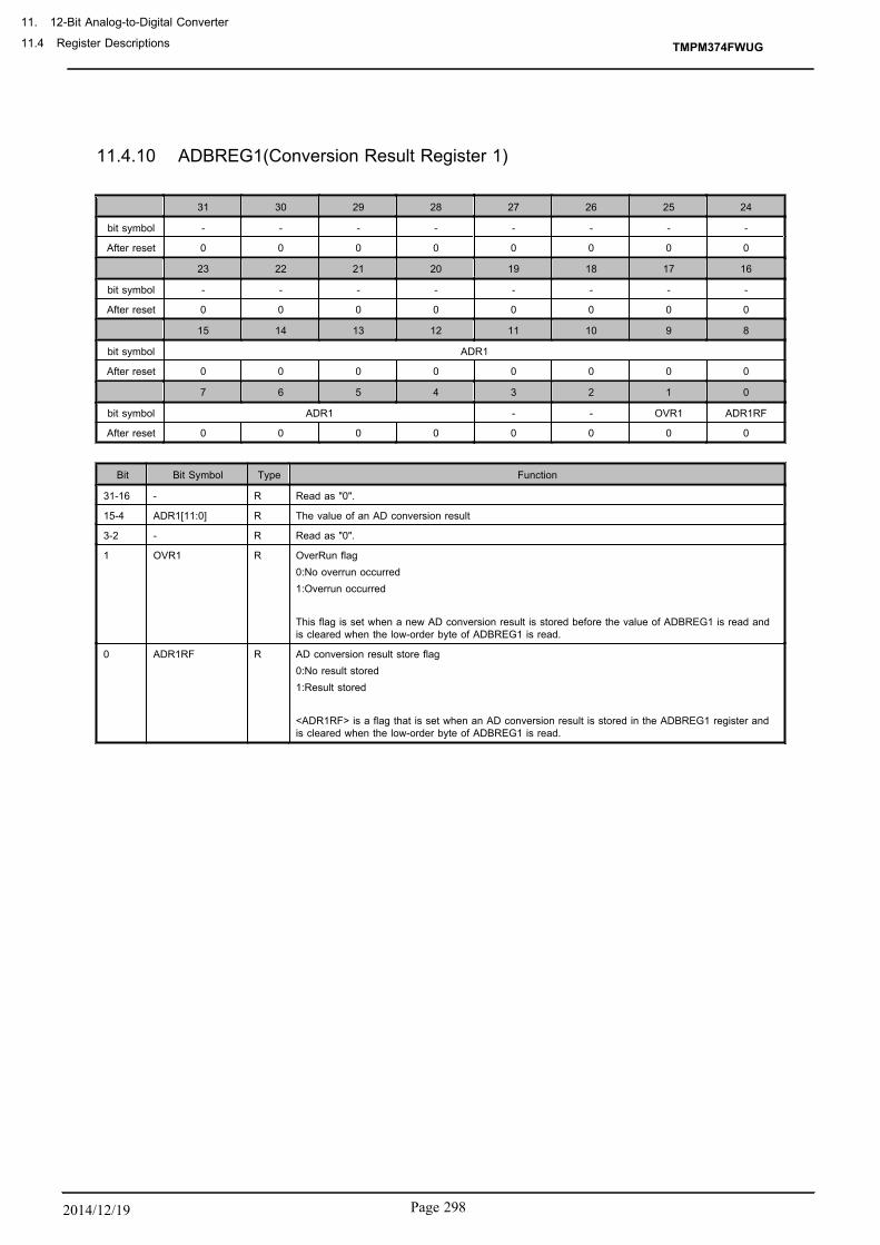
11.4.10 ADBREG1(Conversion Result Register 1)
31 30 29 28 27 26 25 24
bit symbol - - - - - - - -
After reset 0 0 0 0 0 0 0 0
23 22 21 20 19 18 17 16
bit symbol - - - - - - - -
After reset 0 0 0 0 0 0 0 0
15 14 13 12 11 10 9 8
bit symbol ADR1
After reset 0 0 0 0 0 0 0 0
7 6 5 4 3 2 1 0
bit symbol ADR1 - - OVR1 ADR1RF
After reset 0 0 0 0 0 0 0 0
Bit Bit Symbol Type Function
31-16 - R Read as "0".
15-4 ADR1[11:0] R The value of an AD conversion result
3-2 - R Read as "0".
1 OVR1 R OverRun flag0:No overrun occurred1:Overrun occurred This flag is set when a new AD conversion result is stored before the value of ADBREG1 is read andis cleared when the low-order byte of ADBREG1 is read.
0 ADR1RF R AD conversion result store flag0:No result stored1:Result stored <ADR1RF> is a flag that is set when an AD conversion result is stored in the ADBREG1 register andis cleared when the low-order byte of ADBREG1 is read.
TMPM374FWUG
11. 12-Bit Analog-to-Digital Converter
11.4 Register Descriptions
Page 2982014/12/19

11.4.11 ADBREG2(Conversion Result Register 2)
31 30 29 28 27 26 25 24
bit symbol - - - - - - - -
After reset 0 0 0 0 0 0 0 0
23 22 21 20 19 18 17 16
bit symbol - - - - - - - -
After reset 0 0 0 0 0 0 0 0
15 14 13 12 11 10 9 8
bit symbol ADR2
After reset 0 0 0 0 0 0 0 0
7 6 5 4 3 2 1 0
bit symbol ADR2 - - OVR2 ADR2RF
After reset 0 0 0 0 0 0 0 0
Bit Bit Symbol Type Function
31-16 - R Read as "0".
15-4 ADR2[11:0] R The value of an AD conversion result
3-2 - R Read as "0".
1 OVR2 R OverRun flag0:No overrun occurred1:Overrun occurred This flag is set when a new AD conversion result is stored before the value of ADBREG2 is read andis cleared when the low-order byte of ADBREG2 is read.
0 ADR2RF R AD conversion result store flag0:No result stored1:Result stored <ADR2RF> is a flag that is set when an AD conversion result is stored in the ADBREG2 register andis cleared when the low-order byte of ADBREG2 is read.
TMPM374FWUG
Page 299 2014/12/19

11.4.12 ADBREG3(Conversion Result Register 3)
31 30 29 28 27 26 25 24
bit symbol - - - - - - - -
After reset 0 0 0 0 0 0 0 0
23 22 21 20 19 18 17 16
bit symbol - - - - - - - -
After reset 0 0 0 0 0 0 0 0
15 14 13 12 11 10 9 8
bit symbol ADR3
After reset 0 0 0 0 0 0 0 0
7 6 5 4 3 2 1 0
bit symbol ADR3 - - OVR3 ADR3RF
After reset 0 0 0 0 0 0 0 0
Bit Bit Symbol Type Function
31-16 - R Read as "0".
15-4 ADR3[11:0] R The value of an AD conversion result
3-2 - R Read as "0".
1 OVR3 R OverRun flag0:No overrun occurred1:Overrun occurred This flag is set when a new AD conversion result is stored before the value of ADBREG3 is read andis cleared when the low-order byte of ADBREG3 is read.
0 ADR3RF R AD conversion result store flag0:No result stored1:Result stored <ADR3RF> is a flag that is set when an AD conversion result is stored in the ADBREG3 register andis cleared when the low-order byte of ADBREG3 is read.
TMPM374FWUG
11. 12-Bit Analog-to-Digital Converter
11.4 Register Descriptions
Page 3002014/12/19

11.4.13 ADBREG4(Conversion Result Register 4)
31 30 29 28 27 26 25 24
bit symbol - - - - - - - -
After reset 0 0 0 0 0 0 0 0
23 22 21 20 19 18 17 16
bit symbol - - - - - - - -
After reset 0 0 0 0 0 0 0 0
15 14 13 12 11 10 9 8
bit symbol ADR4
After reset 0 0 0 0 0 0 0 0
7 6 5 4 3 2 1 0
bit symbol ADR4 - - OVR4 ADR4RF
After reset 0 0 0 0 0 0 0 0
Bit Bit Symbol Type Function
31-16 - R Read as "0".
15-4 ADR4[11:0] R The value of an AD conversion result
3-2 - R Read as "0".
1 OVR4 R OverRun flag0:No overrun occurred1:Overrun occurred This flag is set when a new AD conversion result is stored before the value of ADBREG4 is read andis cleared when the low-order byte of ADBREG4 is read.
0 ADR4RF R AD conversion result store flag0:No result stored1:Result stored <ADR4RF> is a flag that is set when an AD conversion result is stored in the ADBREG4 register andis cleared when the low-order byte of ADBREG4 is read.
TMPM374FWUG
Page 301 2014/12/19

11.4.14 ADBREG5(Conversion Result Register 5)
31 30 29 28 27 26 25 24
bit symbol - - - - - - - -
After reset 0 0 0 0 0 0 0 0
23 22 21 20 19 18 17 16
bit symbol - - - - - - - -
After reset 0 0 0 0 0 0 0 0
15 14 13 12 11 10 9 8
bit symbol ADR5
After reset 0 0 0 0 0 0 0 0
7 6 5 4 3 2 1 0
bit symbol ADR5 - - OVR5 ADR5RF
After reset 0 0 0 0 0 0 0 0
Bit Bit Symbol Type Function
31-16 - R Read as "0".
15-4 ADR5[11:0] R The value of an AD conversion result
3-2 - R Read as "0".
1 OVR5 R OverRun flag0:No overrun occurred1:Overrun occurred This flag is set when a new AD conversion result is stored before the value of ADBREG5 is read andis cleared when the low-order byte of ADBREG5 is read.
0 ADR5RF R AD conversion result store flag0:No result stored1:Result stored <ADR5RF> is a flag that is set when an AD conversion result is stored in the ADBREG5 register andis cleared when the low-order byte of ADBREG5 is read.
TMPM374FWUG
11. 12-Bit Analog-to-Digital Converter
11.4 Register Descriptions
Page 3022014/12/19
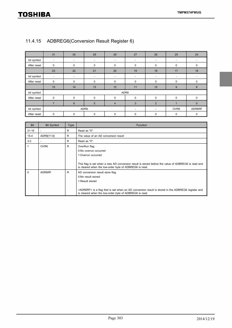
11.4.15 ADBREG6(Conversion Result Register 6)
31 30 29 28 27 26 25 24
bit symbol - - - - - - - -
After reset 0 0 0 0 0 0 0 0
23 22 21 20 19 18 17 16
bit symbol - - - - - - - -
After reset 0 0 0 0 0 0 0 0
15 14 13 12 11 10 9 8
bit symbol ADR6
After reset 0 0 0 0 0 0 0 0
7 6 5 4 3 2 1 0
bit symbol ADR6 - - OVR6 ADR6RF
After reset 0 0 0 0 0 0 0 0
Bit Bit Symbol Type Function
31-16 - R Read as "0".
15-4 ADR6[11:0] R The value of an AD conversion result
3-2 - R Read as "0".
1 OVR6 R OverRun flag0:No overrun occurred1:Overrun occurred This flag is set when a new AD conversion result is stored before the value of ADBREG6 is read andis cleared when the low-order byte of ADBREG6 is read.
0 ADR6RF R AD conversion result store flag0:No result stored1:Result stored <ADR6RF> is a flag that is set when an AD conversion result is stored in the ADBREG6 register andis cleared when the low-order byte of ADBREG6 is read.
TMPM374FWUG
Page 303 2014/12/19

11.4.16 ADxBREG7(Conversion Result Register 7)
31 30 29 28 27 26 25 24
bit symbol - - - - - - - -
After reset 0 0 0 0 0 0 0 0
23 22 21 20 19 18 17 16
bit symbol - - - - - - - -
After reset 0 0 0 0 0 0 0 0
15 14 13 12 11 10 9 8
bit symbol ADR7
After reset 0 0 0 0 0 0 0 0
7 6 5 4 3 2 1 0
bit symbol ADR7 - - OVR7 ADR7RF
After reset 0 0 0 0 0 0 0 0
Bit Bit Symbol Type Function
31-16 - R Read as "0".
15-4 ADR7[11:0] R The value of an AD conversion result
3-2 - R Read as "0".
1 OVR7 R OverRun flag0:No overrun occurred1:Overrun occurred This flag is set when a new AD conversion result is stored before the value of ADBREG7 is read andis cleared when the low-order byte of ADBREG7 is read.
0 ADR7RF R AD conversion result store flag0:No result stored1:Result stored <ADR7RF> is a flag that is set when an AD conversion result is stored in the ADBREG7 register andis cleared when the low-order byte of ADBREG7 is read.
TMPM374FWUG
11. 12-Bit Analog-to-Digital Converter
11.4 Register Descriptions
Page 3042014/12/19

11.4.17 ADBREG8(Conversion Result Register 8)
31 30 29 28 27 26 25 24
bit symbol - - - - - - - -
After reset 0 0 0 0 0 0 0 0
23 22 21 20 19 18 17 16
bit symbol - - - - - - - -
After reset 0 0 0 0 0 0 0 0
15 14 13 12 11 10 9 8
bit symbol ADR8
After reset 0 0 0 0 0 0 0 0
7 6 5 4 3 2 1 0
bit symbol ADR8 - - OVR8 ADR8RF
After reset 0 0 0 0 0 0 0 0
Bit Bit Symbol Type Function
31-16 - R Read as "0".
15-4 ADR8[11:0] R The value of an AD conversion result
3-2 - R Read as "0".
1 OVR8 R OverRun flag0:No overrun occurred1:Overrun occurred This flag is set when a new AD conversion result is stored before the value of ADBREG8 is read andis cleared when the low-order byte of ADBREG8 is read.
0 ADR8RF R AD conversion result store flag0:No result stored1:Result stored <ADR8RF> is a flag that is set when an AD conversion result is stored in the ADBREG8 register andis cleared when the low-order byte of ADBREG8 is read.
TMPM374FWUG
Page 305 2014/12/19

11.4.18 ADBREG9(Conversion Result Register 9)
31 30 29 28 27 26 25 24
bit symbol - - - - - - - -
After reset 0 0 0 0 0 0 0 0
23 22 21 20 19 18 17 16
bit symbol - - - - - - - -
After reset 0 0 0 0 0 0 0 0
15 14 13 12 11 10 9 8
bit symbol ADR9
After reset 0 0 0 0 0 0 0 0
7 6 5 4 3 2 1 0
bit symbol ADR9 - - OVR9 ADR9RF
After reset 0 0 0 0 0 0 0 0
Bit Bit Symbol Type Function
31-16 - R Read as "0".
15-4 ADR9[11:0] R The value of an AD conversion result
3-2 - R Read as "0".
1 OVR9 R OverRun flag0:No overrun occurred1:Overrun occurred This flag is set when a new AD conversion result is stored before the value of ADBREG9 is read andis cleared when the low-order byte of ADBREG9 is read.
0 ADR9RF R AD conversion result store flag0:No result stored1:Result stored <ADR9RF> is a flag that is set when an AD conversion result is stored in the ADBREG9 register andis cleared when the low-order byte of ADBREG9 is read.
TMPM374FWUG
11. 12-Bit Analog-to-Digital Converter
11.4 Register Descriptions
Page 3062014/12/19
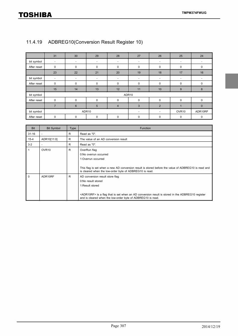
11.4.19 ADBREG10(Conversion Result Register 10)
31 30 29 28 27 26 25 24
bit symbol - - - - - - - -
After reset 0 0 0 0 0 0 0 0
23 22 21 20 19 18 17 16
bit symbol - - - - - - - -
After reset 0 0 0 0 0 0 0 0
15 14 13 12 11 10 9 8
bit symbol ADR10
After reset 0 0 0 0 0 0 0 0
7 6 5 4 3 2 1 0
bit symbol ADR10 - - OVR10 ADR10RF
After reset 0 0 0 0 0 0 0 0
Bit Bit Symbol Type Function
31-16 - R Read as "0".
15-4 ADR10[11:0] R The value of an AD conversion result
3-2 - R Read as "0".
1 OVR10 R OverRun flag0:No overrun occurred1:Overrun occurred This flag is set when a new AD conversion result is stored before the value of ADBREG10 is read andis cleared when the low-order byte of ADBREG10 is read.
0 ADR10RF R AD conversion result store flag0:No result stored1:Result stored <ADR10RF> is a flag that is set when an AD conversion result is stored in the ADBREG10 registerand is cleared when the low-order byte of ADBREG10 is read.
TMPM374FWUG
Page 307 2014/12/19

11.4.20 ADBREG11(Conversion Result Register 11)
31 30 29 28 27 26 25 24
bit symbol - - - - - - - -
After reset 0 0 0 0 0 0 0 0
23 22 21 20 19 18 17 16
bit symbol - - - - - - - -
After reset 0 0 0 0 0 0 0 0
15 14 13 12 11 10 9 8
bit symbol ADR11
After reset 0 0 0 0 0 0 0 0
7 6 5 4 3 2 1 0
bit symbol ADR11 - - OVR11 ADR11RF
After reset 0 0 0 0 0 0 0 0
Bit Bit Symbol Type Function
31-16 - R Read as "0".
15-4 ADR11[11:0] R The value of an AD conversion result
3-2 - R Read as "0".
1 OVR11 R OverRun flag0:No overrun occurred1:Overrun occurred This flag is set when a new AD conversion result is stored before the value of ADBREG11 is read andis cleared when the low-order byte of ADBREG11 is read.
0 ADR11RF R AD conversion result store flag0:No result stored1:Result stored <ADR11RF> is a flag that is set when an AD conversion result is stored in the ADBREG11 registerand is cleared when the low-order byte of ADBREG11 is read.
TMPM374FWUG
11. 12-Bit Analog-to-Digital Converter
11.4 Register Descriptions
Page 3082014/12/19
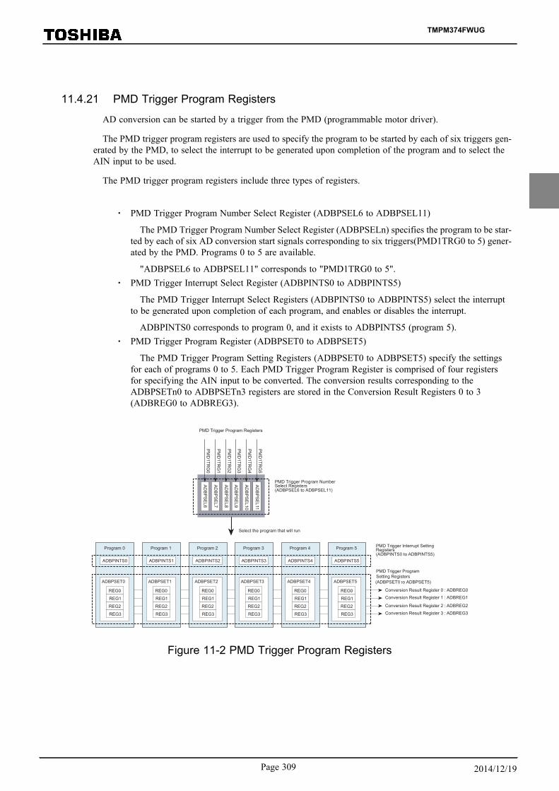
11.4.21 PMD Trigger Program Registers
AD conversion can be started by a trigger from the PMD (programmable motor driver).
The PMD trigger program registers are used to specify the program to be started by each of six triggers gen-erated by the PMD, to select the interrupt to be generated upon completion of the program and to select theAIN input to be used.
The PMD trigger program registers include three types of registers.
・ PMD Trigger Program Number Select Register (ADBPSEL6 to ADBPSEL11)
The PMD Trigger Program Number Select Register (ADBPSELn) specifies the program to be star-ted by each of six AD conversion start signals corresponding to six triggers(PMD1TRG0 to 5) gener-ated by the PMD. Programs 0 to 5 are available.
"ADBPSEL6 to ADBPSEL11" corresponds to "PMD1TRG0 to 5".・ PMD Trigger Interrupt Select Register (ADBPINTS0 to ADBPINTS5)
The PMD Trigger Interrupt Select Registers (ADBPINTS0 to ADBPINTS5) select the interruptto be generated upon completion of each program, and enables or disables the interrupt.
ADBPINTS0 corresponds to program 0, and it exists to ADBPINTS5 (program 5).・ PMD Trigger Program Register (ADBPSET0 to ADBPSET5)
The PMD Trigger Program Setting Registers (ADBPSET0 to ADBPSET5) specify the settingsfor each of programs 0 to 5. Each PMD Trigger Program Register is comprised of four registersfor specifying the AIN input to be converted. The conversion results corresponding to theADBPSETn0 to ADBPSETn3 registers are stored in the Conversion Result Registers 0 to 3(ADBREG0 to ADBREG3).
PMD Trigger Program Number Select Registers(ADBPSEL6 to ADBPSEL11)
PMD Trigger Program Registers
AD
BP
SE
L6
AD
BP
SE
L8
AD
BP
SE
L7
AD
BP
SE
L10
AD
BP
SE
L11
AD
BP
SE
L9
PM
D1TR
G0
PM
D1TR
G2
PM
D1TR
G1
PM
D1TR
G4
PM
D1TR
G5
PM
D1TR
G3
PMD Trigger Interrupt Setting Registers(ADBPINTS0 to ADBPINTS5)
PMD Trigger ProgramSetting Registers(ADBPSET0 to ADBPSET5)
Conversion Result Register 0 : ADBREG0
Program 0
ADBPINTS0
ADBPSET0
REG0
REG1
REG2
REG3
Program 3
ADBPINTS3
ADBPSET3
REG0
REG1
REG2
REG3
Program 4
ADBPINTS4
ADBPSET4
REG0
REG1
REG2
REG3
Program 5
ADBPINTS5
ADBPSET5
REG0
REG1
REG2
REG3
Program 2
ADBPINTS2
ADBPSET2
REG0
REG1
REG2
REG3
Program 1
ADBPINTS1
ADBPSET1
REG0
REG1
REG2
REG3
Select the program that will run
Conversion Result Register 1 : ADBREG1
Conversion Result Register 2 : ADBREG2
Conversion Result Register 3 : ADBREG3
Figure 11-2 PMD Trigger Program Registers
TMPM374FWUG
Page 309 2014/12/19

11.4.21.1 ADBPSEL6 to ADBPSEL11(PMD Trigger Program Number Select Register 6 to 11)
ADBPSEL0:PMD Trigger Program Number Select Register 0
31 30 29 28 27 26 25 24
bit symbol - - - - - - - -
After reset 0 0 0 0 0 0 0 0
23 22 21 20 19 18 17 16
bit symbol - - - - - - - -
After reset 0 0 0 0 0 0 0 0
15 14 13 12 11 10 9 8
bit symbol - - - - - - - -
After reset 0 0 0 0 0 0 0 0
7 6 5 4 3 2 1 0
bit symbol PENS0 - - - - PMDS0
After reset 0 0 0 0 0 0 0 0
Bit Bit Symbol Type Function
31-8 - R Read as "0".
7 PENS0 R/W PMD0TRG0 trigger controll0:Disable1:Enable
6-3 - R Read as "0".
2-0 PMDS0[2:0] R/W Program number select (Refer to Table 11-1)
ADBPSEL1:PMD Trigger Program Number Select Register 1
31 30 29 28 27 26 25 24
bit symbol - - - - - - - -
After reset 0 0 0 0 0 0 0 0
23 22 21 20 19 18 17 16
bit symbol - - - - - - - -
After reset 0 0 0 0 0 0 0 0
15 14 13 12 11 10 9 8
bit symbol - - - - - - - -
After reset 0 0 0 0 0 0 0 0
7 6 5 4 3 2 1 0
bit symbol PENS1 - - - - PMDS1
After reset 0 0 0 0 0 0 0 0
Bit Bit Symbol Type Function
31-8 - R Read as "0".
7 PENS1 R/W PMD0TRG1 trigger control0:Disable1:Enable
6-3 - R Read as "0".
2-0 PMDS1[2:0] R/W Program number select (Refer to Table 11-1)
TMPM374FWUG
11. 12-Bit Analog-to-Digital Converter
11.4 Register Descriptions
Page 3102014/12/19

ADBPSEL2:PMD Trigger Program Number Select Register 2
31 30 29 28 27 26 25 24
bit symbol - - - - - - - -
After reset 0 0 0 0 0 0 0 0
23 22 21 20 19 18 17 16
bit symbol - - - - - - - -
After reset 0 0 0 0 0 0 0 0
15 14 13 12 11 10 9 8
bit symbol - - - - - - - -
After reset 0 0 0 0 0 0 0 0
7 6 5 4 3 2 1 0
bit symbol PENS2 - - - - PMDS2
After reset 0 0 0 0 0 0 0 0
Bit Bit Symbol Type Function
31-8 - R Read as "0".
7 PENS2 R/W PMD0TRG2 trigger control0:Disable1:Enable
6-3 - R Read as "0".
2-0 PMDS2[2:0] R/W Program number select (Refer to Table 11-1)
ADBPSEL3:PMD Trigger Program Number Select Register 3
31 30 29 28 27 26 25 24
bit symbol - - - - - - - -
After reset 0 0 0 0 0 0 0 0
23 22 21 20 19 18 17 16
bit symbol - - - - - - - -
After reset 0 0 0 0 0 0 0 0
15 14 13 12 11 10 9 8
bit symbol - - - - - - - -
After reset 0 0 0 0 0 0 0 0
7 6 5 4 3 2 1 0
bit symbol PENS3 - - - - PMDS3
After reset 0 0 0 0 0 0 0 0
Bit Bit Symbol Type Function
31-8 - R Read as "0".
7 PENS3 R/W PMD0TRG3 trigger control0:Disable1:Enable
6-3 - R Read as "0".
2-0 PMDS3[2:0] R/W Program number select (Refer to Table 11-1)
TMPM374FWUG
Page 311 2014/12/19

ADBPSEL4:PMD Trigger Program Number Select Register 4
31 30 29 28 27 26 25 24
bit symbol - - - - - - - -
After reset 0 0 0 0 0 0 0 0
23 22 21 20 19 18 17 16
bit symbol - - - - - - - -
After reset 0 0 0 0 0 0 0 0
15 14 13 12 11 10 9 8
bit symbol - - - - - - - -
After reset 0 0 0 0 0 0 0 0
7 6 5 4 3 2 1 0
bit symbol PENS4 - - - - PMDS4
After reset 0 0 0 0 0 0 0 0
Bit Bit Symbol Type Function
31-8 - R Read as "0".
7 PENS4 R/W PMD0TRG4 trigger control0:Disable1:Enable
6-3 - R Read as "0".
2-0 PMDS4[2:0] R/W Program number select (Refer to Table 11-1)
ADBPSEL5:PMD Trigger Program Number Select Register 5
31 30 29 28 27 26 25 24
bit symbol - - - - - - - -
After reset 0 0 0 0 0 0 0 0
23 22 21 20 19 18 17 16
bit symbol - - - - - - - -
After reset 0 0 0 0 0 0 0 0
15 14 13 12 11 10 9 8
bit symbol - - - - - - - -
After reset 0 0 0 0 0 0 0 0
7 6 5 4 3 2 1 0
bit symbol PENS5 - - - - PMDS5
After reset 0 0 0 0 0 0 0 0
Bit Bit Symbol Type Function
31-8 - R Read as "0".
7 PENS5 R/W PMD0TRG5 trigger control0:Disable1:Enable
6-3 - R Read as "0".
2-0 PMDS5[2:0] R/W Program number select (Refer to Table 11-1)
TMPM374FWUG
11. 12-Bit Analog-to-Digital Converter
11.4 Register Descriptions
Page 3122014/12/19

ADBPSEL6:PMD Trigger Program Number Select Register 6
31 30 29 28 27 26 25 24
bit symbol - - - - - - - -
After reset 0 0 0 0 0 0 0 0
23 22 21 20 19 18 17 16
bit symbol - - - - - - - -
After reset 0 0 0 0 0 0 0 0
15 14 13 12 11 10 9 8
bit symbol - - - - - - - -
After reset 0 0 0 0 0 0 0 0
7 6 5 4 3 2 1 0
bit symbol PENS6 - - - - PMDS6
After reset 0 0 0 0 0 0 0 0
Bit Bit Symbol Type Function
31-8 - R Read as "0".
7 PENS6 R/W PMD1TRG0 trigger control0:Disable1:Enable
6-3 - R Read as "0".
2-0 PMDS6[2:0] R/W Program number select (Refer to Table 11-1)
ADBPSEL7:PMD Trigger Program Number Select Register 7
31 30 29 28 27 26 25 24
bit symbol - - - - - - - -
After reset 0 0 0 0 0 0 0 0
23 22 21 20 19 18 17 16
bit symbol - - - - - - - -
After reset 0 0 0 0 0 0 0 0
15 14 13 12 11 10 9 8
bit symbol - - - - - - - -
After reset 0 0 0 0 0 0 0 0
7 6 5 4 3 2 1 0
bit symbol PENS7 - - - - PMDS7
After reset 0 0 0 0 0 0 0 0
Bit Bit Symbol Type Function
31-8 - R Read as "0".
7 PENS7 R/W PMD1TRG1 trigger control0:Disable1:Enable
6-3 - R Read as "0".
2-0 PMDS7[2:0] R/W Program number select (Refer to Table 11-1)
TMPM374FWUG
Page 313 2014/12/19

ADBPSEL8:PMD Trigger Program Number Select Register 8
31 30 29 28 27 26 25 24
bit symbol - - - - - - - -
After reset 0 0 0 0 0 0 0 0
23 22 21 20 19 18 17 16
bit symbol - - - - - - - -
After reset 0 0 0 0 0 0 0 0
15 14 13 12 11 10 9 8
bit symbol - - - - - - - -
After reset 0 0 0 0 0 0 0 0
7 6 5 4 3 2 1 0
bit symbol PENS8 - - - - PMDS8
After reset 0 0 0 0 0 0 0 0
Bit Bit Symbol Type Function
31-8 - R Read as "0".
7 PENS8 R/W PMD1TRG2 trigger control0:Disable1:Enable
6-3 - R Read as "0".
2-0 PMDS8[2:0] R/W Program number select (Refer to Table 11-1)
ADBPSEL9:PMD Trigger Program Number Select Register 9
31 30 29 28 27 26 25 24
bit symbol - - - - - - - -
After reset 0 0 0 0 0 0 0 0
23 22 21 20 19 18 17 16
bit symbol - - - - - - - -
After reset 0 0 0 0 0 0 0 0
15 14 13 12 11 10 9 8
bit symbol - - - - - - - -
After reset 0 0 0 0 0 0 0 0
7 6 5 4 3 2 1 0
bit symbol PENS9 - - - - PMDS9
After reset 0 0 0 0 0 0 0 0
Bit Bit Symbol Type Function
31-8 - R Read as "0".
7 PENS9 R/W PMD1TRG3 trigger control0:Disable1:Enable
6-3 - R Read as "0".
2-0 PMDS9[2:0] R/W Program number select (Refer to Table 11-1)
TMPM374FWUG
11. 12-Bit Analog-to-Digital Converter
11.4 Register Descriptions
Page 3142014/12/19

ADBPSEL10:PMD Trigger Program Number Select Register 10
31 30 29 28 27 26 25 24
bit symbol - - - - - - - -
After reset 0 0 0 0 0 0 0 0
23 22 21 20 19 18 17 16
bit symbol - - - - - - - -
After reset 0 0 0 0 0 0 0 0
15 14 13 12 11 10 9 8
bit symbol - - - - - - - -
After reset 0 0 0 0 0 0 0 0
7 6 5 4 3 2 1 0
bit symbol PENS10 - - - - PMDS10
After reset 0 0 0 0 0 0 0 0
Bit Bit Symbol Type Function
31-8 - R Read as "0".
7 PENS10 R/W PMD1TRG4 trigger control0:Disable1:Enable
6-3 - R Read as "0".
2-0 PMDS10[2:0] R/W Program number select (Refer to Table 11-1)
ADBPSEL11:PMD Trigger Program Number Select Register 11
31 30 29 28 27 26 25 24
bit symbol - - - - - - - -
After reset 0 0 0 0 0 0 0 0
23 22 21 20 19 18 17 16
bit symbol - - - - - - - -
After reset 0 0 0 0 0 0 0 0
15 14 13 12 11 10 9 8
bit symbol - - - - - - - -
After reset 0 0 0 0 0 0 0 0
7 6 5 4 3 2 1 0
bit symbol PENS11 - - - - PMDS11
After reset 0 0 0 0 0 0 0 0
Bit Bit Symbol Type Function
31-8 - R Read as "0".
7 PENS11 R/W PMD1TRG5 trigger control0:Disable1:Enable
6-3 - R Read as "0".
2-0 PMDS11[2:0] R/W Program number select (Refer to Table 11-1)
TMPM374FWUG
Page 315 2014/12/19

Table 11-1 Program number select
<PMDS6[2:0]>~<PMDS11[2:0]>
000 Program0
001 Program1
010 Program2
011 Program3
100 Program4
101 Program5
110 reserved
111 reserved
TMPM374FWUG
11. 12-Bit Analog-to-Digital Converter
11.4 Register Descriptions
Page 3162014/12/19

11.4.21.2 ADBPINTS0 to 5(PMD Trigger Interrupt Select Register 0 to 5)
ADxPINTS0:PMD Trigger Interrupt Select Register 0
31 30 29 28 27 26 25 24
bit symbol - - - - - - - -
After reset 0 0 0 0 0 0 0 0
23 22 21 20 19 18 17 16
bit symbol - - - - - - - -
After reset 0 0 0 0 0 0 0 0
15 14 13 12 11 10 9 8
bit symbol - - - - - - - -
After reset 0 0 0 0 0 0 0 0
7 6 5 4 3 2 1 0
bit symbol - - - - - - INTSEL0
After reset 0 0 0 0 0 0 0 0
Bit Bit Symbol Type Function
31-2 - R Read as "0".
1-0 INTSEL0[1:0] R/W Interrupt select00:No interrupt output01:Reserved10:INTADBPDB11: No interrupt output
The starting interrupt is selected for program 0.
ADBPINTS1:PMD Trigger Interrupt Select Register 1
31 30 29 28 27 26 25 24
bit symbol - - - - - - - -
After reset 0 0 0 0 0 0 0 0
23 22 21 20 19 18 17 16
bit symbol - - - - - - - -
After reset 0 0 0 0 0 0 0 0
15 14 13 12 11 10 9 8
bit symbol - - - - - - - -
After reset 0 0 0 0 0 0 0 0
7 6 5 4 3 2 1 0
bit symbol - - - - - - INTSEL1
After reset 0 0 0 0 0 0 0 0
Bit Bit Symbol Type Function
31-2 - R Read as "0".
1-0 INTSEL1[1:0] R/W Interrupt select00:No interrupt output01:Reserved10:INTADBPDB11: No interrupt output
The starting interrupt is selected for program 1.
TMPM374FWUG
Page 317 2014/12/19

ADBPINTS2:PMD Trigger Interrupt Select Register 2
31 30 29 28 27 26 25 24
bit symbol - - - - - - - -
After reset 0 0 0 0 0 0 0 0
23 22 21 20 19 18 17 16
bit symbol - - - - - - - -
After reset 0 0 0 0 0 0 0 0
15 14 13 12 11 10 9 8
bit symbol - - - - - - - -
After reset 0 0 0 0 0 0 0 0
7 6 5 4 3 2 1 0
bit symbol - - - - - - INTSEL2
After reset 0 0 0 0 0 0 0 0
Bit Bit Symbol Type Function
31-2 - R Read as "0".
1-0 INTSEL2[1:0] R/W Interrupt select00:No interrupt output01:Reserved10:INTADBPDB11: No interrupt output
The starting interrupt is selected for program 2.
ADBPINTS3:PMD Trigger Interrupt Select Register 3
31 30 29 28 27 26 25 24
bit symbol - - - - - - - -
After reset 0 0 0 0 0 0 0 0
23 22 21 20 19 18 17 16
bit symbol - - - - - - - -
After reset 0 0 0 0 0 0 0 0
15 14 13 12 11 10 9 8
bit symbol - - - - - - - -
After reset 0 0 0 0 0 0 0 0
7 6 5 4 3 2 1 0
bit symbol - - - - - - INTSEL3
After reset 0 0 0 0 0 0 0 0
Bit Bit Symbol Type Function
31-2 - R Read as "0".
1-0 INTSEL3[1:0] R/W Interrupt select00:No interrupt output01:Reserved10:INTADBPDB11: No interrupt output
The starting interrupt is selected for program 3.
TMPM374FWUG
11. 12-Bit Analog-to-Digital Converter
11.4 Register Descriptions
Page 3182014/12/19
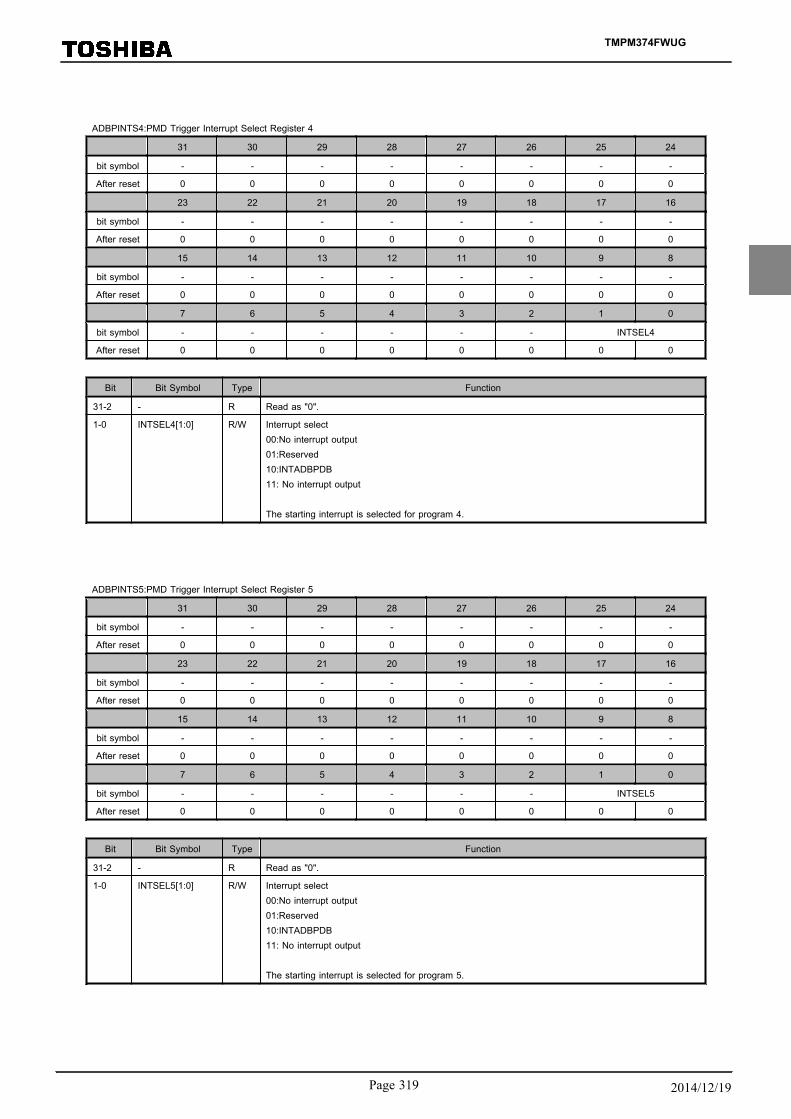
ADBPINTS4:PMD Trigger Interrupt Select Register 4
31 30 29 28 27 26 25 24
bit symbol - - - - - - - -
After reset 0 0 0 0 0 0 0 0
23 22 21 20 19 18 17 16
bit symbol - - - - - - - -
After reset 0 0 0 0 0 0 0 0
15 14 13 12 11 10 9 8
bit symbol - - - - - - - -
After reset 0 0 0 0 0 0 0 0
7 6 5 4 3 2 1 0
bit symbol - - - - - - INTSEL4
After reset 0 0 0 0 0 0 0 0
Bit Bit Symbol Type Function
31-2 - R Read as "0".
1-0 INTSEL4[1:0] R/W Interrupt select00:No interrupt output01:Reserved10:INTADBPDB11: No interrupt output
The starting interrupt is selected for program 4.
ADBPINTS5:PMD Trigger Interrupt Select Register 5
31 30 29 28 27 26 25 24
bit symbol - - - - - - - -
After reset 0 0 0 0 0 0 0 0
23 22 21 20 19 18 17 16
bit symbol - - - - - - - -
After reset 0 0 0 0 0 0 0 0
15 14 13 12 11 10 9 8
bit symbol - - - - - - - -
After reset 0 0 0 0 0 0 0 0
7 6 5 4 3 2 1 0
bit symbol - - - - - - INTSEL5
After reset 0 0 0 0 0 0 0 0
Bit Bit Symbol Type Function
31-2 - R Read as "0".
1-0 INTSEL5[1:0] R/W Interrupt select00:No interrupt output01:Reserved10:INTADBPDB11: No interrupt output
The starting interrupt is selected for program 5.
TMPM374FWUG
Page 319 2014/12/19
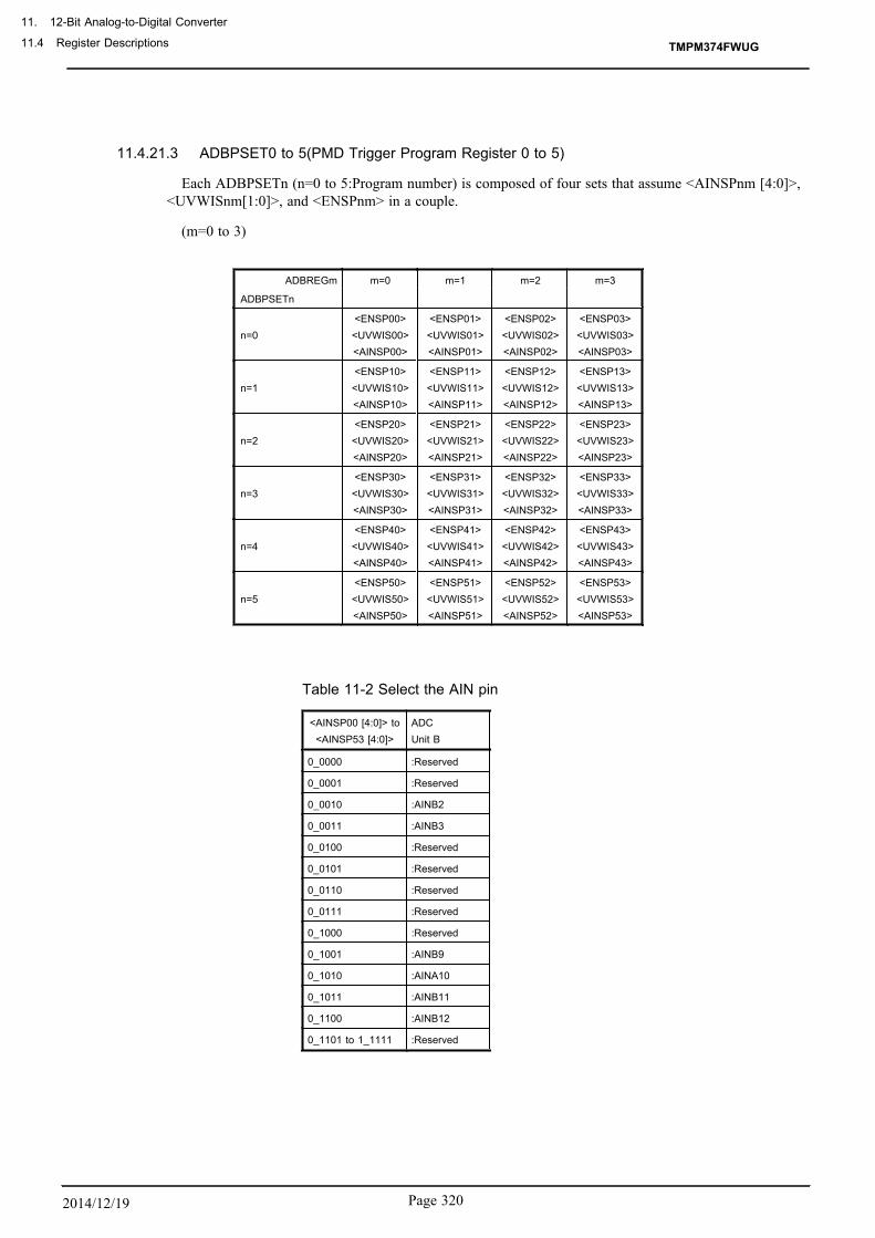
11.4.21.3 ADBPSET0 to 5(PMD Trigger Program Register 0 to 5)
Each ADBPSETn (n=0 to 5:Program number) is composed of four sets that assume <AINSPnm [4:0]>,<UVWISnm[1:0]>, and <ENSPnm> in a couple.
(m=0 to 3)
ADBREGm m=0 m=1 m=2 m=3
ADBPSETn
n=0<ENSP00><UVWIS00><AINSP00>
<ENSP01><UVWIS01><AINSP01>
<ENSP02><UVWIS02><AINSP02>
<ENSP03><UVWIS03><AINSP03>
n=1<ENSP10><UVWIS10><AINSP10>
<ENSP11><UVWIS11><AINSP11>
<ENSP12><UVWIS12><AINSP12>
<ENSP13><UVWIS13><AINSP13>
n=2<ENSP20><UVWIS20><AINSP20>
<ENSP21><UVWIS21><AINSP21>
<ENSP22><UVWIS22><AINSP22>
<ENSP23><UVWIS23><AINSP23>
n=3<ENSP30><UVWIS30><AINSP30>
<ENSP31><UVWIS31><AINSP31>
<ENSP32><UVWIS32><AINSP32>
<ENSP33><UVWIS33><AINSP33>
n=4<ENSP40><UVWIS40><AINSP40>
<ENSP41><UVWIS41><AINSP41>
<ENSP42><UVWIS42><AINSP42>
<ENSP43><UVWIS43><AINSP43>
n=5<ENSP50><UVWIS50><AINSP50>
<ENSP51><UVWIS51><AINSP51>
<ENSP52><UVWIS52><AINSP52>
<ENSP53><UVWIS53><AINSP53>
Table 11-2 Select the AIN pin
<AINSP00 [4:0]> to<AINSP53 [4:0]>
ADCUnit B
0_0000 :Reserved
0_0001 :Reserved
0_0010 :AINB2
0_0011 :AINB3
0_0100 :Reserved
0_0101 :Reserved
0_0110 :Reserved
0_0111 :Reserved
0_1000 :Reserved
0_1001 :AINB9
0_1010 :AINA10
0_1011 :AINB11
0_1100 :AINB12
0_1101 to 1_1111 :Reserved
TMPM374FWUG
11. 12-Bit Analog-to-Digital Converter
11.4 Register Descriptions
Page 3202014/12/19

ADBPSET0:PMD Trigger Program Register 0
31 30 29 28 27 26 25 24
bit symbol ENSP03 UVWIS03 AINSP03
After reset 0 0 0 0 0 0 0 0
23 22 21 20 19 18 17 16
bit symbol ENSP02 UVWIS02 AINSP02
After reset 0 0 0 0 0 0 0 0
15 14 13 12 11 10 9 8
bit symbol ENSP01 UVWIS01 AINSP01
After reset 0 0 0 0 0 0 0 0
7 6 5 4 3 2 1 0
bit symbol ENSP00 UVWIS00 AINSP00
After reset 0 0 0 0 0 0 0 0
Bit Bit Symbol Type Function
31 ENSP03 R/W ADBREG3 enable0:Disable1:Enable
30-29 UVWIS03[1:0] R/W Phase select (for Vector Engine)See table below.
28-24 AINSP03[4:0] R/W AIN select
Refer to "Table 11-2 Select the AIN pin".
23 ENSP02 R/W ADBREG2 enable0:Disable1:Enable
22-21 UVWIS02[1:0] R/W Phase select (for Vector Engine)See table below.
20-16 AINSP02[4:0] R/W AIN select
Refer to "Table 11-2 Select the AIN pin".
15 ENSP01 R/W ADBREG1 enable0:Disable1:Enable
14-13 UVWIS01[1:0] R/W Phase select (for Vector Engine)See table below.
12-8 AINSP01[4:0] R/W AIN select
Refer to "Table 11-2 Select the AIN pin".
7 ENSP00 R/W ADBREG0 enable0:Disable1:Enable
6-5 UVWIS00[1:0] R/W Phase select (for Vector Engine)See table below.
4-0 AINSP00[4:0] R/W AIN select
Refer to "Table 11-2 Select the AIN pin".
Phase select
00 Not specified
01 U
10 V
11 W
TMPM374FWUG
Page 321 2014/12/19

ADBPSET1:PMD Trigger Program Register 1
31 30 29 28 27 26 25 24
bit symbol ENSP13 UVWIS13 AINSP13
After reset 0 0 0 0 0 0 0 0
23 22 21 20 19 18 17 16
bit symbol ENSP12 UVWIS12 AINSP12
After reset 0 0 0 0 0 0 0 0
15 14 13 12 11 10 9 8
bit symbol ENSP11 UVWIS11 AINSP11
After reset 0 0 0 0 0 0 0 0
7 6 5 4 3 2 1 0
bit symbol ENSP10 UVWIS10 AINSP10
After reset 0 0 0 0 0 0 0 0
Bit Bit Symbol Type Function
31 ENSP13 R/W ADBREG3 enable0:Disable1:Enable
30-29 UVWIS13[1:0] R/W Phase select (for Vector Engine)See table below.
28-24 AINSP13[4:0] R/W AIN select
Refer to "Table 11-2 Select the AIN pin".
23 ENSP12 R/W ADBREG2 enable0:Disable1:Enable
22-21 UVWIS12[1:0] R/W Phase select (for Vector Engine)See table below.
20-16 AINSP12[4:0] R/W AIN select
Refer to "Table 11-2 Select the AIN pin".
15 ENSP11 R/W ADBREG1 enable0:Disable1:Enable
14-13 UVWIS11[1:0] R/W Phase select (for Vector Engine)See table below.
12-8 AINSP11[4:0] R/W AIN select
Refer to "Table 11-2 Select the AIN pin".
7 ENSP10 R/W ADBREG0 enable0:Disable1:Enable
6-5 UVWIS10[1:0] R/W Phase select (for Vector Engine)See table below.
4-0 AINSP10[4:0] R/W AIN select
Refer to "Table 11-2 Select the AIN pin".
Phase select
00 Not specified
01 U
10 V
11 W
TMPM374FWUG
11. 12-Bit Analog-to-Digital Converter
11.4 Register Descriptions
Page 3222014/12/19

ADBPSET2:PMD Trigger Program Register 2
31 30 29 28 27 26 25 24
bit symbol ENSP23 UVWIS23 AINSP23
After reset 0 0 0 0 0 0 0 0
23 22 21 20 19 18 17 16
bit symbol ENSP22 UVWIS22 AINSP22
After reset 0 0 0 0 0 0 0 0
15 14 13 12 11 10 9 8
bit symbol ENSP21 UVWIS21 AINSP21
After reset 0 0 0 0 0 0 0 0
7 6 5 4 3 2 1 0
bit symbol ENSP20 UVWIS20 AINSP20
After reset 0 0 0 0 0 0 0 0
Bit Bit Symbol Type Function
31 ENSP23 R/W ADBREG3 enable0:Disable1:Enable
30-29 UVWIS23[1:0] R/W Phase select (for Vector Engine)See table below.
28-24 AINSP23[4:0] R/W AIN select
Refer to "Table 11-2 Select the AIN pin".
23 ENSP22 R/W ADBREG2 enable0:Disable1:Enable
22-21 UVWIS22[1:0] R/W Phase select (for Vector Engine)See table below.
20-16 AINSP22[4:0] R/W AIN select
Refer to "Table 11-2 Select the AIN pin".
15 ENSP21 R/W ADBREG1 enable0:Disable1:Enable
14-13 UVWIS21[1:0] R/W Phase select (for Vector Engine)See table below.
12-8 AINSP21[4:0] R/W AIN select
Refer to "Table 11-2 Select the AIN pin".
7 ENSP20 R/W ADBREG0 enable0:Disable1:Enable
6-5 UVWIS20[1:0] R/W Phase select (for Vector Engine)See table below.
4-0 AINSP20[4:0] R/W AIN select
Refer to "Table 11-2 Select the AIN pin".
Phase select
00 Not specified
01 U
10 V
11 W
TMPM374FWUG
Page 323 2014/12/19

ADBPSET3:PMD Trigger Program Register 3
31 30 29 28 27 26 25 24
bit symbol ENSP33 UVWIS33 AINSP33
After reset 0 0 0 0 0 0 0 0
23 22 21 20 19 18 17 16
bit symbol ENSP32 UVWIS32 AINSP32
After reset 0 0 0 0 0 0 0 0
15 14 13 12 11 10 9 8
bit symbol ENSP31 UVWIS31 AINSP31
After reset 0 0 0 0 0 0 0 0
7 6 5 4 3 2 1 0
bit symbol ENSP30 UVWIS30 AINSP30
After reset 0 0 0 0 0 0 0 0
Bit Bit Symbol Type Function
31 ENSP33 R/W ADBREG3 enable0:Disable1:Enable
30-29 UVWIS33[1:0] R/W Phase select (for Vector Engine)See table below.
28-24 AINSP33[4:0] R/W AIN select
Refer to "Table 11-2 Select the AIN pin".
23 ENSP32 R/W ADBREG2 enable0:Disable1:Enable
22-21 UVWIS32[1:0] R/W Phase select (for Vector Engine)See table below.
20-16 AINSP32[4:0] R/W AIN select
Refer to "Table 11-2 Select the AIN pin".
15 ENSP31 R/W ADBREG1 enable0:Disable1:Enable
14-13 UVWIS31[1:0] R/W Phase select (for Vector Engine)See table below.
12-8 AINSP31[4:0] R/W AIN select
Refer to "Table 11-2 Select the AIN pin".
7 ENSP30 R/W ADBREG0 enable0:Disable1:Enable
6-5 UVWIS30[1:0] R/W Phase select (for Vector Engine)See table below.
4-0 AINSP30[4:0] R/W AIN select
Refer to "Table 11-2 Select the AIN pin".
Phase select
00 Not specified
01 U
10 V
11 W
TMPM374FWUG
11. 12-Bit Analog-to-Digital Converter
11.4 Register Descriptions
Page 3242014/12/19

ADBPSET4:PMD Trigger Program Register 4
31 30 29 28 27 26 25 24
bit symbol ENSP43 UVWIS43 AINSP43
After reset 0 0 0 0 0 0 0 0
23 22 21 20 19 18 17 16
bit symbol ENSP42 UVWIS42 AINSP42
After reset 0 0 0 0 0 0 0 0
15 14 13 12 11 10 9 8
bit symbol ENSP41 UVWIS41 AINSP41
After reset 0 0 0 0 0 0 0 0
7 6 5 4 3 2 1 0
bit symbol ENSP40 UVWIS40 AINSP40
After reset 0 0 0 0 0 0 0 0
Bit Bit Symbol Type Function
31 ENSP43 R/W ADBREG3 enable0:Disable1:Enable
30-29 UVWIS43[1:0] R/W Phase select (for Vector Engine)See table below.
28-24 AINSP43[4:0] R/W AIN select
Refer to "Table 11-2 Select the AIN pin".
23 ENSP42 R/W ADBREG2 enable0:Disable1:Enable
22-21 UVWIS42[1:0] R/W Phase select (for Vector Engine)See table below.
20-16 AINSP42[4:0] R/W AIN select
Refer to "Table 11-2 Select the AIN pin".
15 ENSP41 R/W ADBREG1 enable0:Disable1:Enable
14-13 UVWIS41[1:0] R/W Phase select (for Vector Engine)See table below.
12-8 AINSP41[4:0] R/W AIN select
Refer to "Table 11-2 Select the AIN pin".
7 ENSP40 R/W ADBREG0 enable0:Disable1:Enable
6-5 UVWIS40[1:0] R/W Phase select (for Vector Engine)See table below.
4-0 AINSP40[4:0] R/W AIN select
Refer to "Table 11-2 Select the AIN pin".
Phase select
00 Not specified
01 U
10 V
11 W
TMPM374FWUG
Page 325 2014/12/19

ADBPSET5:PMD Trigger Program Register 5
31 30 29 28 27 26 25 24
bit symbol ENSP53 UVWIS53 AINSP53
After reset 0 0 0 0 0 0 0 0
23 22 21 20 19 18 17 16
bit symbol ENSP52 UVWIS52 AINSP52
After reset 0 0 0 0 0 0 0 0
15 14 13 12 11 10 9 8
bit symbol ENSP51 UVWIS51 AINSP51
After reset 0 0 0 0 0 0 0 0
7 6 5 4 3 2 1 0
bit symbol ENSP50 UVWIS50 AINSP50
After reset 0 0 0 0 0 0 0 0
Bit Bit Symbol Type Function
31 ENSP53 R/W ADBREG3 enable0:Disable1:Enable
30-29 UVWIS53[1:0] R/W Phase select (for Vector Engine)See table below.
28-24 AINSP53[4:0] R/W AIN select
Refer to "Table 11-2 Select the AIN pin".
23 ENSP52 R/W ADBREG2 enable0:Disable1:Enable
22-21 UVWIS52[1:0] R/W Phase select (for Vector Engine)See table below.
20-16 AINSP52[4:0] R/W AIN select
Refer to "Table 11-2 Select the AIN pin".
15 ENSP51 R/W ADBREG1 enable0:Disable1:Enable
14-13 UVWIS51[1:0] R/W Phase select (for Vector Engine)See table below.
12-8 AINSP51[4:0] R/W AIN select
Refer to "Table 11-2 Select the AIN pin".
7 ENSP50 R/W ADBREG0 enable0:Disable1:Enable
6-5 UVWIS50[1:0] R/W Phase select (for Vector Engine)See table below.
4-0 AINSP50[4:0] R/W AIN select
Refer to "Table 11-2 Select the AIN pin".
Phase select
00 Not specified
01 U
10 V
11 W
TMPM374FWUG
11. 12-Bit Analog-to-Digital Converter
11.4 Register Descriptions
Page 3262014/12/19
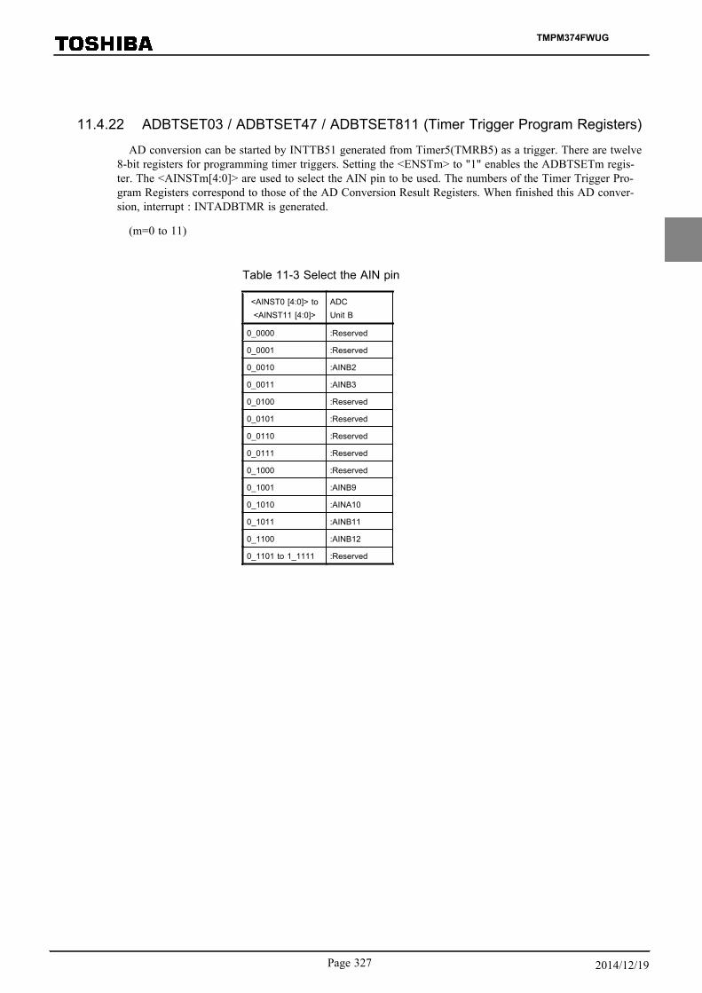
11.4.22 ADBTSET03 / ADBTSET47 / ADBTSET811 (Timer Trigger Program Registers)
AD conversion can be started by INTTB51 generated from Timer5(TMRB5) as a trigger. There are twelve8-bit registers for programming timer triggers. Setting the <ENSTm> to "1" enables the ADBTSETm regis-ter. The <AINSTm[4:0]> are used to select the AIN pin to be used. The numbers of the Timer Trigger Pro-gram Registers correspond to those of the AD Conversion Result Registers. When finished this AD conver-sion, interrupt : INTADBTMR is generated.
(m=0 to 11)
Table 11-3 Select the AIN pin
<AINST0 [4:0]> to<AINST11 [4:0]>
ADCUnit B
0_0000 :Reserved
0_0001 :Reserved
0_0010 :AINB2
0_0011 :AINB3
0_0100 :Reserved
0_0101 :Reserved
0_0110 :Reserved
0_0111 :Reserved
0_1000 :Reserved
0_1001 :AINB9
0_1010 :AINA10
0_1011 :AINB11
0_1100 :AINB12
0_1101 to 1_1111 :Reserved
TMPM374FWUG
Page 327 2014/12/19

ADBTSET03: Timer Trigger Program Registers 03
31 30 29 28 27 26 25 24
bit symbol ENST3 - - AINST3
After reset 0 0 0 0 0 0 0 0
23 22 21 20 19 18 17 16
bit symbol ENST2 - - AINST2
After reset 0 0 0 0 0 0 0 0
15 14 13 12 11 10 9 8
bit symbol ENST1 - - AINST1
After reset 0 0 0 0 0 0 0 0
7 6 5 4 3 2 1 0
bit symbol ENST0 - - AINST0
After reset 0 0 0 0 0 0 0 0
Bit Bit Symbol Type Function
31 ENST3 R/W ADBREG3 enable0:Disable1:Enable
30-29 - R Read as "0".
28-24 AINST3[4:0] R/W AIN select
Refer to "Table 11-3 Select the AIN pin".
23 ENST2 R/W ADBREG2 enable0:Disable1:Enable
22-21 - R Read as "0".
20-16 AINST2[4:0] R/W AIN select
Refer to "Table 11-3 Select the AIN pin".
15 ENST1 R/W ADBREG1 enable0:Disable1:Enable
14-13 - R Read as "0".
12-8 AINST1[4:0] R/W AIN select
Refer to "Table 11-3 Select the AIN pin".
7 ENST0 R/W ADBREG0 enable0:Disable1:Enable
6-5 - R Read as "0".
4-0 AINST0[4:0] R/W AIN select
Refer to "Table 11-3 Select the AIN pin".
TMPM374FWUG
11. 12-Bit Analog-to-Digital Converter
11.4 Register Descriptions
Page 3282014/12/19

ADBTSET47: Timer Trigger Program Registers 47
31 30 29 28 27 26 25 24
bit symbol ENST7 - - AINST7
After reset 0 0 0 0 0 0 0 0
23 22 21 20 19 18 17 16
bit symbol ENST6 - - AINST6
After reset 0 0 0 0 0 0 0 0
15 14 13 12 11 10 9 8
bit symbol ENST5 - - AINST5
After reset 0 0 0 0 0 0 0 0
7 6 5 4 3 2 1 0
bit symbol ENST4 - - AINST4
After reset 0 0 0 0 0 0 0 0
Bit Bit Symbol Type Function
31 ENST7 R/W ADBREG7 enable0:Disable1:Enable
30-29 - R Read as "0".
28-24 AINST7[4:0] R/W AIN select
Refer to "Table 11-3 Select the AIN pin".
23 ENST6 R/W ADBREG6 enable0:Disable1:Enable
22-21 - R Read as "0".
20-16 AINST6[4:0] R/W AIN select
Refer to "Table 11-3 Select the AIN pin".
15 ENST5 R/W ADBREG5 enable0:Disable1:Enable
14-13 - R Read as "0".
12-8 AINST5[4:0] R/W AIN select
Refer to "Table 11-3 Select the AIN pin".
7 ENST4 R/W ADBREG4 enable0:Disable1:Enable
6-5 - R Read as "0".
4-0 AINST4[4:0] R/W AIN select
Refer to "Table 11-3 Select the AIN pin".
TMPM374FWUG
Page 329 2014/12/19

ADBTSET811: Timer Trigger Program Registers 811
31 30 29 28 27 26 25 24
bit symbol ENST11 - - AINST11
After reset 0 0 0 0 0 0 0 0
23 22 21 20 19 18 17 16
bit symbol ENST10 - - AINST10
After reset 0 0 0 0 0 0 0 0
15 14 13 12 11 10 9 8
bit symbol ENST9 - - AINST9
After reset 0 0 0 0 0 0 0 0
7 6 5 4 3 2 1 0
bit symbol ENST8 - - AINST8
After reset 0 0 0 0 0 0 0 0
Bit Bit Symbol Type Function
31 ENST11 R/W ADBREG11 enable0:Disable1:Enable
30-29 - R Read as "0".
28-24 AINST11[4:0] R/W AIN select
Refer to "Table 11-3 Select the AIN pin".
23 ENST10 R/W ADBREG10 enable0:Disable1:Enable
22-21 - R Read as "0".
20-16 AINST10[4:0] R/W AIN select
Refer to "Table 11-3 Select the AIN pin".
15 ENST9 R/W ADBREG9 enable0:Disable1:Enable
14-13 - R Read as "0".
12-8 AINST9[4:0] R/W AIN select
Refer to "Table 11-3 Select the AIN pin".
7 ENST8 R/W ADBREG8 enable0:Disable1:Enable
6-5 - R Read as "0".
4-0 AINST8[4:0] R/W AIN select
Refer to "Table 11-3 Select the AIN pin".
TMPM374FWUG
11. 12-Bit Analog-to-Digital Converter
11.4 Register Descriptions
Page 3302014/12/19
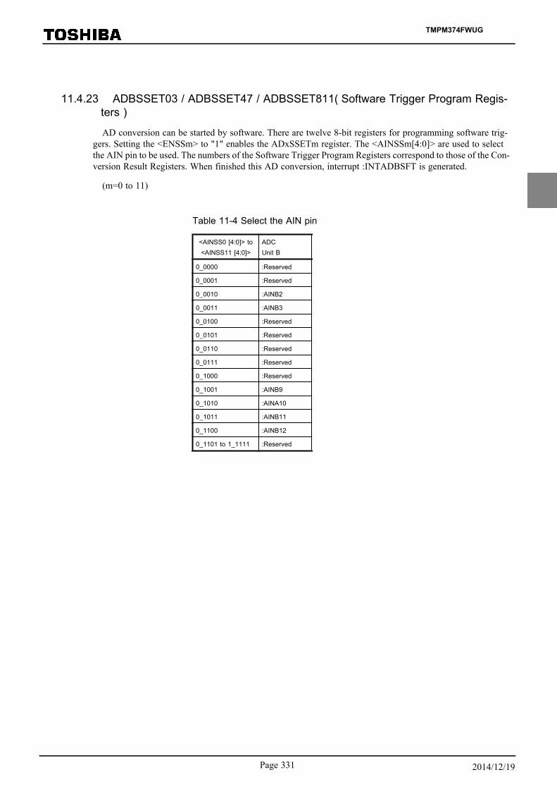
11.4.23 ADBSSET03 / ADBSSET47 / ADBSSET811( Software Trigger Program Regis-ters )
AD conversion can be started by software. There are twelve 8-bit registers for programming software trig-gers. Setting the <ENSSm> to "1" enables the ADxSSETm register. The <AINSSm[4:0]> are used to selectthe AIN pin to be used. The numbers of the Software Trigger Program Registers correspond to those of the Con-version Result Registers. When finished this AD conversion, interrupt :INTADBSFT is generated.
(m=0 to 11)
Table 11-4 Select the AIN pin
<AINSS0 [4:0]> to<AINSS11 [4:0]>
ADCUnit B
0_0000 :Reserved
0_0001 :Reserved
0_0010 :AINB2
0_0011 :AINB3
0_0100 :Reserved
0_0101 :Reserved
0_0110 :Reserved
0_0111 :Reserved
0_1000 :Reserved
0_1001 :AINB9
0_1010 :AINA10
0_1011 :AINB11
0_1100 :AINB12
0_1101 to 1_1111 :Reserved
TMPM374FWUG
Page 331 2014/12/19
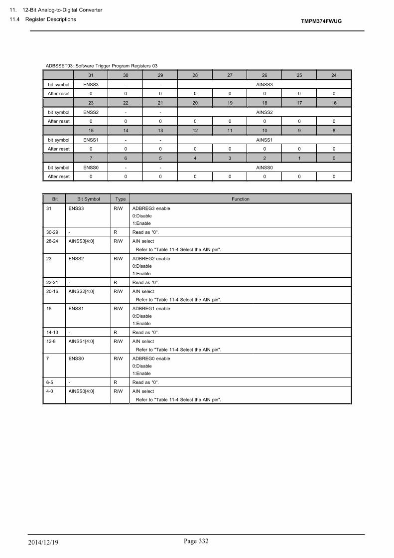
ADBSSET03: Software Trigger Program Registers 03
31 30 29 28 27 26 25 24
bit symbol ENSS3 - - AINSS3
After reset 0 0 0 0 0 0 0 0
23 22 21 20 19 18 17 16
bit symbol ENSS2 - - AINSS2
After reset 0 0 0 0 0 0 0 0
15 14 13 12 11 10 9 8
bit symbol ENSS1 - - AINSS1
After reset 0 0 0 0 0 0 0 0
7 6 5 4 3 2 1 0
bit symbol ENSS0 - - AINSS0
After reset 0 0 0 0 0 0 0 0
Bit Bit Symbol Type Function
31 ENSS3 R/W ADBREG3 enable0:Disable1:Enable
30-29 - R Read as "0".
28-24 AINSS3[4:0] R/W AIN select
Refer to "Table 11-4 Select the AIN pin".
23 ENSS2 R/W ADBREG2 enable0:Disable1:Enable
22-21 - R Read as "0".
20-16 AINSS2[4:0] R/W AIN select
Refer to "Table 11-4 Select the AIN pin".
15 ENSS1 R/W ADBREG1 enable0:Disable1:Enable
14-13 - R Read as "0".
12-8 AINSS1[4:0] R/W AIN select
Refer to "Table 11-4 Select the AIN pin".
7 ENSS0 R/W ADBREG0 enable0:Disable1:Enable
6-5 - R Read as "0".
4-0 AINSS0[4:0] R/W AIN select
Refer to "Table 11-4 Select the AIN pin".
TMPM374FWUG
11. 12-Bit Analog-to-Digital Converter
11.4 Register Descriptions
Page 3322014/12/19

ADBSSET47: Software Trigger Program Registers 47
31 30 29 28 27 26 25 24
bit symbol ENSS7 - - AINSS7
After reset 0 0 0 0 0 0 0 0
23 22 21 20 19 18 17 16
bit symbol ENSS6 - - AINSS6
After reset 0 0 0 0 0 0 0 0
15 14 13 12 11 10 9 8
bit symbol ENSS5 - - AINSS5
After reset 0 0 0 0 0 0 0 0
7 6 5 4 3 2 1 0
bit symbol ENSS4 - - AINSS4
After reset 0 0 0 0 0 0 0 0
Bit Bit Symbol Type Function
31 ENSS7 R/W ADBREG7 enable0:Disable1:Enable
30-29 - R Read as "0".
28-24 AINSS7[4:0] R/W AIN select
Refer to "Table 11-4 Select the AIN pin".
23 ENSS6 R/W ADBREG6 enable0:Disable1:Enable
22-21 - R Read as "0".
20-16 AINSS6[4:0] R/W AIN select
Refer to "Table 11-4 Select the AIN pin".
15 ENSS5 R/W ADBREG5 enable0:Disable1:Enable
14-13 - R Read as "0".
12-8 AINSS5[4:0] R/W AIN select
Refer to "Table 11-4 Select the AIN pin".
7 ENSS4 R/W ADBREG4 enable0:Disable1:Enable
6-5 - R Read as "0".
4-0 AINSS4[4:0] R/W AIN select
Refer to "Table 11-4 Select the AIN pin".
TMPM374FWUG
Page 333 2014/12/19

ADBSSET811: Software Trigger Program Registers 811
31 30 29 28 27 26 25 24
bit symbol ENSS11 - - AINSS11
After reset 0 0 0 0 0 0 0 0
23 22 21 20 19 18 17 16
bit symbol ENSS10 - - AINSS10
After reset 0 0 0 0 0 0 0 0
15 14 13 12 11 10 9 8
bit symbol ENSS9 - - AINSS9
After reset 0 0 0 0 0 0 0 0
7 6 5 4 3 2 1 0
bit symbol ENSS8 - - AINSS8
After reset 0 0 0 0 0 0 0 0
Bit Bit Symbol Type Function
31 ENSS11 R/W ADBREG11 enable0:Disable1:Enable
30-29 - R Read as "0".
28-24 AINSS11[4:0] R/W AIN select
Refer to "Table 11-4 Select the AIN pin".
23 ENSS10 R/W ADBREG10 enable0:Disable1:Enable
22-21 - R Read as "0".
20-16 AINSS10[4:0] R/W AIN select
Refer to "Table 11-4 Select the AIN pin".
15 ENSS9 R/W ADBREG9 enable0:Disable1:Enable
14-13 - R Read as "0".
12-8 AINSS9[4:0] R/W AIN select
Refer to "Table 11-4 Select the AIN pin".
7 ENSS8 R/W ADBREG8 enable0:Disable1:Enable
6-5 - R Read as "0".
4-0 AINSS8[4:0] R/W AIN select
Refer to "Table 11-4 Select the AIN pin".
TMPM374FWUG
11. 12-Bit Analog-to-Digital Converter
11.4 Register Descriptions
Page 3342014/12/19
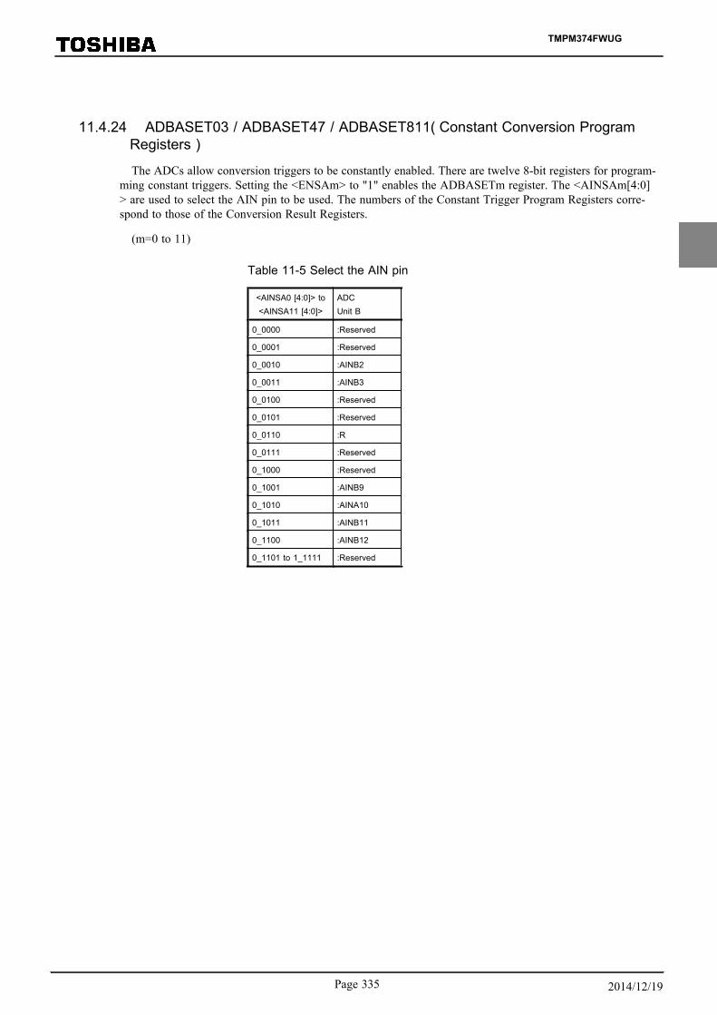
11.4.24 ADBASET03 / ADBASET47 / ADBASET811( Constant Conversion ProgramRegisters )
The ADCs allow conversion triggers to be constantly enabled. There are twelve 8-bit registers for program-ming constant triggers. Setting the <ENSAm> to "1" enables the ADBASETm register. The <AINSAm[4:0]> are used to select the AIN pin to be used. The numbers of the Constant Trigger Program Registers corre-spond to those of the Conversion Result Registers.
(m=0 to 11)
Table 11-5 Select the AIN pin
<AINSA0 [4:0]> to<AINSA11 [4:0]>
ADCUnit B
0_0000 :Reserved
0_0001 :Reserved
0_0010 :AINB2
0_0011 :AINB3
0_0100 :Reserved
0_0101 :Reserved
0_0110 :R
0_0111 :Reserved
0_1000 :Reserved
0_1001 :AINB9
0_1010 :AINA10
0_1011 :AINB11
0_1100 :AINB12
0_1101 to 1_1111 :Reserved
TMPM374FWUG
Page 335 2014/12/19

ADBASET03: Constant Conversion Program Registers03
31 30 29 28 27 26 25 24
bit symbol ENSA3 - - AINSA3
After reset 0 0 0 0 0 0 0 0
23 22 21 20 19 18 17 16
bit symbol ENSA2 - - AINSA2
After reset 0 0 0 0 0 0 0 0
15 14 13 12 11 10 9 8
bit symbol ENSA1 - - AINSA1
After reset 0 0 0 0 0 0 0 0
7 6 5 4 3 2 1 0
bit symbol ENSA0 - - AINSA0
After reset 0 0 0 0 0 0 0 0
Bit Bit Symbol Type Function
31 ENSA3 R/W ADBREG3 enable0:Disable1:Enable
30-29 - R Read as "0".
28-24 AINSA3[4:0] R/W AIN select
Refer to "Table 11-5 Select the AIN pin".
23 ENSA2 R/W ADBREG2 enable0:Disable1:Enable
22-21 - R Read as "0".
20-16 AINSA2[4:0] R/W AIN select
Refer to "Table 11-5 Select the AIN pin".
15 ENSA1 R/W ADBREG1 enable0:Disable1:Enable
14-13 - R Read as "0".
12-8 AINSA1[4:0] R/W AIN select
Refer to "Table 11-5 Select the AIN pin".
7 ENSA0 R/W ADBREG0 enable0:Disable1:Enable
6-5 - R Read as "0".
4-0 AINSA0[4:0] R/W AIN select
Refer to "Table 11-5 Select the AIN pin".
TMPM374FWUG
11. 12-Bit Analog-to-Digital Converter
11.4 Register Descriptions
Page 3362014/12/19
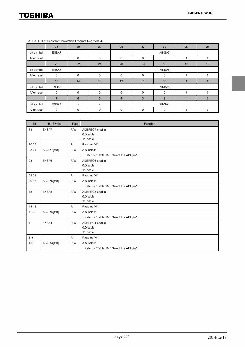
ADBASET47: Constant Conversion Program Registers 47
31 30 29 28 27 26 25 24
bit symbol ENSA7 - - AINSA7
After reset 0 0 0 0 0 0 0 0
23 22 21 20 19 18 17 16
bit symbol ENSA6 - - AINSA6
After reset 0 0 0 0 0 0 0 0
15 14 13 12 11 10 9 8
bit symbol ENSA5 - - AINSA5
After reset 0 0 0 0 0 0 0 0
7 6 5 4 3 2 1 0
bit symbol ENSA4 - - AINSA4
After reset 0 0 0 0 0 0 0 0
Bit Bit Symbol Type Function
31 ENSA7 R/W ADBREG7 enable0:Disable1:Enable
30-29 - R Read as "0".
28-24 AINSA7[4:0] R/W AIN select
Refer to "Table 11-5 Select the AIN pin".
23 ENSA6 R/W ADBREG6 enable0:Disable1:Enable
22-21 - R Read as "0".
20-16 AINSA6[4:0] R/W AIN select
Refer to "Table 11-5 Select the AIN pin".
15 ENSA5 R/W ADBREG5 enable0:Disable1:Enable
14-13 - R Read as "0".
12-8 AINSA5[4:0] R/W AIN select
Refer to "Table 11-5 Select the AIN pin".
7 ENSA4 R/W ADBREG4 enable0:Disable1:Enable
6-5 - R Read as "0".
4-0 AINSA4[4:0] R/W AIN select
Refer to "Table 11-5 Select the AIN pin".
TMPM374FWUG
Page 337 2014/12/19

ADBASET811: Cnstant Conversion Program Registers 811
31 30 29 28 27 26 25 24
bit symbol ENSA11 - - AINSA11
After reset 0 0 0 0 0 0 0 0
23 22 21 20 19 18 17 16
bit symbol ENSA10 - - AINSA10
After reset 0 0 0 0 0 0 0 0
15 14 13 12 11 10 9 8
bit symbol ENSA9 - - AINSA9
After reset 0 0 0 0 0 0 0 0
7 6 5 4 3 2 1 0
bit symbol ENSA8 - - AINSA8
After reset 0 0 0 0 0 0 0 0
Bit Bit Symbol Type Function
31 ENSA11 R/W ADBREG11 enable0:Disable1:Enable
30-29 - R Read as "0".
28-24 AINSA11[4:0] R/W AIN select
Refer to "Table 11-5 Select the AIN pin".
23 ENSA10 R/W ADBREG10 enable0:Disable1:Enable
22-21 - R Read as "0".
20-16 AINSA10[4:0] R/W AIN select
Refer to "Table 11-5 Select the AIN pin".
15 ENSA9 R/W ADBREG9 enable0:Disable1:Enable
14-13 - R Read as "0".
12-8 AINSA9[4:0] R/W AIN select
Refer to "Table 11-5 Select the AIN pin".
7 ENSA8 R/W ADBREG8 enable0:Disable1:Enable
6-5 - R Read as "0".
4-0 AINSA8[4:0] R/W AIN select
Refer to "Table 11-5 Select the AIN pin".
TMPM374FWUG
11. 12-Bit Analog-to-Digital Converter
11.4 Register Descriptions
Page 3382014/12/19

11.5 Operation Descriptions
11.5.1 Analog Reference Voltages
For the High-level and Low-level analog reference voltages, the VREFHB and VREFLB pins are used inADC B. There are no registers for controlling current between VREFHB and VREFLB. Inputs to these pinsare fixed.
Note 1: During AD conversion, do not change the output data of port I/J/K, to avoid the influence on the conver-sion result.
Note 2: AD conversion results might be unstable by the following conditions.Input operation is executed.Output operation is executed.Output current of port varies.Take a countermeasure such as averaging the multiple conversion results, to get precise value.
11.5.2 Starting AD Conversion
AD conversion is started by software or one of the following three trigger signals.
These start triggers are given priorities as shown below.
PMD trigger 0 > …・ > PMD trigger 5 > Timer trigger >Softwaretrigger
>constanttrigger
If the PMD trigger occurs while an AD conversion is in progress, the PMD trigger is handled stop the ongo-ing program and start AD conversion correspond to PMD trigger number.
If a higher-priority trigger occurs while an AD conversion is in progress, the higher-priority trigger is han-dled after the ongoing program is completed.
It has some delay from generation of trigger to start of AD conversion. The delay depends on the trigger.The following timing chart and table show the delay.
Trigger
Busy flag<ADBFN>
AD conversion resultregister0(ADxBREG0)
AD conversion resultregister1(ADxBREG1)
1st conversion 2nd conversion
Result of 1st conversion
Result of 2nd conversion
Delay time from trigger AD conversion time Delay time
to the nextconversion
AD conversion time
Figure 11-3 Timing chart of AD conversion
TMPM374FWUG
Page 339 2014/12/19
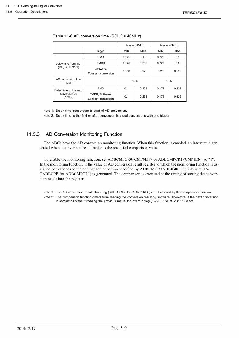
Table 11-6 AD conversion time (SCLK = 40MHz)
fsys = 80MHz fsys = 40MHz
Trigger MIN MAX MIN MAX
Delay time from trig-ger [μs] (Note 1)
PMD 0.125 0.163 0.225 0.3
TMRB 0.125 0.263 0.225 0.5
Software,Constant conversion
0.138 0.275 0.25 0.525
AD conversion time[μs] − 1.85 1.85
Delay time to the nextconversion[μs]
(Note2)
PMD 0.1 0.125 0.175 0.225
TMRB, Software,Constant conversion
0.1 0.238 0.175 0.425
Note 1: Delay time from trigger to start of AD conversion.Note 2: Delay time to the 2nd or after conversion in plural conversions with one trigger.
11.5.3 AD Conversion Monitoring Function
The ADCs have the AD conversion monitoring function. When this function is enabled, an interrupt is gen-erated when a conversion result matches the specified comparison value.
To enable the monitoring function, set ADBCMPCR0<CMP0EN> or ADBCMPCR1<CMP1EN> to "1".In the monitoring function, if the value of AD conversion result register to which the monitoring function is as-signed corresponds to the comparison condition specified by ADBCMCR<ADBIG0>, the interrupt (IN-TADBCPB for ADBCMPCR1) is generated. The comparison is executed at the timing of storing the conver-sion result into the register.
Note 1: The AD conversion result store flag (<ADR0RF> to <ADR11RF>) is not cleared by the comparison function.Note 2: The comparison function differs from reading the conversion result by software. Therefore, if the next conversion
is completed without reading the previous result, the overrun flag (<OVR0> to <OVR11>) is set.
TMPM374FWUG
11. 12-Bit Analog-to-Digital Converter
11.5 Operation Descriptions
Page 3402014/12/19

11.6 Timing chart of AD conversionThe following shows a timing chart of software trigger conversion, constant conversion and acceptance of trigger.
11.6.1 Software trigger Conversion
In the software trigger conversion, the interrupt is generated after completion of conversion programmedby ADBSSET03, ADBSSET47 and ADBSSET811.(Figure 11-4)
If the ADBMOD1<ADEN> is cleared to "0" during AD conversion, the ongoing conversion stops withoutstoring to the result register.(Figure 11-5)
Software triggerconversion(<ADSS>="1")
AINB9conversion
AINB10conversion
AINB11conversion
AINB12conversion
AD conversion
AD conversionbusy flag<ADBFN>
Software conversionbusy flag<ADSFN>
Software trigger ADconversion interrupt(INTADBSFT)
Busy flag variesaccording to conversion
INTADSFT is generated bythe completition of selectedAD conversion at the timingof clearing of ADSFN="0".
ConditionSoftware trigger setting : AINB9, AINB10, AINB11, AINB12
Figure 11-4 Software trigger AD conversion
Software triggerconversion(<ADSS>="1")
AINB9 conversion
Result register for AINB9
AINB10 conversionAD conversionbusy flag<ADBFN>
AD conversionresult register
ADSFN is cleared to “0” immediatelyafter clearing ADEN to “0” .
AD conversionEnable/Disable<ADEN>
The result of AINB9is stored to the resultregister.
The conversion of AINB11 doesn’ t start.
Software conversionbusy flag<ADSFN>
ConditionSoftware trigger setting : AINB9, AINB10, AINB11
Clearing of <ADBFN> is delayed.
The result of AINB10 is notstored to the result register.
Figure 11-5 Writing "0" to <ADEN> during the software trigger AD conversion
TMPM374FWUG
Page 341 2014/12/19

11.6.2 Constant Conversion
In the constant conversion, if the next conversion completes without reading the previous result from the con-version result register, the overrun flag is set to "1". In this case, the previous conversion result in the conver-sion result register is overwritten by the next result. The overrun flag is cleared by reading of the conversion re-sult.(Figure 11-6)
AINB9 conversion
AINB9 conversion
AINB9 conversion
AINB9 conversion
AINB9 conversionAD conversion
AD conversionbusy flag<ADBFN>
Reading of the resultregister(16bit)
3rd result is read.
Constant conversioncontrol(<ADAS>="1")
1st result of AINB9 2nd result of AINB9 3rd result of AINB9 4th result of AINB9
AD conversion resultstore flag<ADR10RF>
Over Run flag<OVR10>
Over Run flag is setcaused by no readingof 1st result.
Reading of 2nd result makesOver Run flag cleared.
2nd result is read.
AD conversionresult register
ConditionConstant conversion setting : AINB9
Figure 11-6 Constant conversion
TMPM374FWUG
11. 12-Bit Analog-to-Digital Converter
11.6 Timing chart of AD conversion
Page 3422014/12/19

11.6.3 AD conversion by trigger
If the PMD trigger is occurred during the software trigger conversion, the ongoing conversion stops imme-diately.(Figure 11-7) If the timer trigger is occurred during the software trigger conversion, the ongoing conver-sion stops after the completion of ongoing conversion. (Figure 11-8) After the completion of conversion by trig-ger, the software trigger conversion starts from the beginning programmed by ADBSSET03, ADBSSET47and ADBSSET811.(Figure 11-9)
AINB9 conversionby software trigger
Max250ns
AD conversion bysoftware trigger
AD conversion AINB10conversionby softwaretrigger
PMD trigger
AINB12 conversion byPMD trigger
The conversion of AINB10 is stoppedby PMD trigger and starts theconversion trigger by PMD.
AD conversion by PMD trigger
Software triggerconversion interruptINTADBSFT
The interrupt isgenerated aftercompletion of thesoftware ADconversion.
AINB9 to AINB11conversion bysoftware trigger
ConditionSoftware trigger setting : AINB9, AINB10, AINB11PMD trigger setting : AINB12
AD conversion bysoftware triggerPMD trigger conversion
interrupt (INTADPDx)(When the interrupt isenabled by ADBPINTS
Figure 11-7 AD conversion by PMD trigger
AD conversion bysoftware trigger
AD conversion
Timer trigger
AD conversionresult register
Result register for AINB9 Result register for AINB10
The conversion by timer triggerwill start after completion ofthe current conversion.
AINB9 conversionby software trigger
AINB10 conversionby timer trigger
Timer trigger ADconversion interruptINTADBTMR
AINB9 conversionby software trigger
Result registerfor AINB9
Software trigger ADconversion interruptINTADBSFT
The interrupt is generatedby the completion of the timertrigger AD conversion.
The interrupt is generatedby the completion of thesoftware AD conversion.
ConditionSoftware trigger setting : AINB9Timer trigger setting : AINB10
AD conversion bytimer trigger
AD conversion bysoftware trigger
The interrupt is not generated by timer triggerwhile in software trigger AD conversion.Even after completion of the AD conversion.
Figure 11-8 AD conversion by timer trigger (1)
TMPM374FWUG
Page 343 2014/12/19
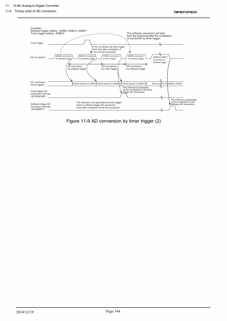
AD conversion AINB9 conversionby software trigger
Timer trigger
The conversion by timer triggerwill start after completion ofthe current conversion.
AD conversionby software trigger
AD conversionby software trigger
AD conversionby timer trigger
AINB10 conversionby software trigger
AINB12 conversionby timer trigger
AINB9 conversionby software trigger
The software conversion will startfrom the beginning after the completionof conversion by timer trigger.
Result register for AINB9 Result register for AINB10 Result register for AINB12AD conversionresult register
Timer trigger ADconversion interruptINTADBTMR
Software trigger ADconversion interruptINTADBSFT
The interrupt is generatedby the completion of the timertrigger AD conversion.
The interrupt is generatedby the completion of thesoftware AD conversion.
AINB9 to AINB11conversion bysoftware trigger
Result register for AINB9 to AINB11
ConditionSoftware trigger setting : AINB9, AINB10, AINB11Timer trigger setting : AINB12
The interrupt is not generated by timer triggerwhile in software trigger AD conversion.Even after completion of the AD conversion.
Figure 11-9 AD conversion by timer trigger (2)
TMPM374FWUG
11. 12-Bit Analog-to-Digital Converter
11.6 Timing chart of AD conversion
Page 3442014/12/19

12. Motor Control Circuit (PMD: Programmable Motor Driver)
The TMPM374FWUG contains 1 channel programmable motor driver (PMD). The PMD of this product has new-ly added features of conduction output control and DC overvoltage detection to realize sensorless motor controland supports interaction with the AD converter.
CPU
IO Bus I/F
PMD
Interrupt
VE
ADC
Interrupt
Analog InputConduction output
PWM/Trigger setting
ADC Sync Trigger
ConversionResult
Interrupt
EMG detection
input
Overvoltage
Detection Input Motor current,Moter voltageEMG1 OVV1
UO1,VO1,WO1,XO1,YO1,ZO1
Figure 12-1 Motor Control-related Block Constitution
TMPM374FWUG
Page 345 2014/12/19

12.1 PMD Input/Output SignalsThe table below shows the signals that are input to and output from PMD.
Table 12-1 Input/Output Signals
Channe Pin Name PMD Signal Name Description
PMD1
PG7/OVV1 OVV 1 OVV state signal
PG6/EMG1 EMG 1 EMG state signal
PG0/UO1 UO 1 U-phase output
PG1/XO1 XO 1 X-phase output
PG2/VO1 VO 1 V-phase output
PG3/YO1 YO 1 Y-phase output
PG4/WO1 WO 1 W-phase output
PG5/ZO1 ZO 1 Z-phase output
TMPM374FWUG
12. Motor Control Circuit (PMD: Programmable Motor Driver)
12.1 PMD Input/Output Signals
Page 3462014/12/19

12.2 PMD Circuit
PORTEN
Wave Generation Circuit
PulseWidthModulation
ConductionContorol
ProtectionContorol
DeadTimeContorol
UX
VY
WZ
ux
vy
wz
SyncTriggerGeneration
VE
PMDTRG0
PMDTRG1
PMDTRG2
PMDTRG3
PMDTRG4
PMDTRG5
VE
UPEQUSDNEQUS
INTPWM
PWMU
PWMV
PWMW
PTENC
Sync Trigger Generation Circuitt
VE
PMD1EMGCRPMD1OVVCR
INTOVV1
PMD1MDCR PMD1MDOUT PMD1DTR PMD1MDPOT
PMD1MDPR
PMD1EMGREL
PMD1CMPU
PMD1CMPV
PMD1CMPW
PMD1TRGCMP0
PMD1TRGCMP1
PMD1TRGCMP2
PMD1TRGCMP3
PMD1TRGCR
UO1
XO1
VO1
YO1
WO1
ZO1
EMG1
INTEMG1
OVV1
PMD1MDCNT
Figure 12-2 Block diagram of PMD Circuit
The PMD circuit consists of two blocks of a wave generation circuit and a sync trigger generation circuit.
The wave generation circuit includes a pulse width modulation circuit, a conduction control circuit, a protectioncontrol circuit, a dead time control circuit.
・ The pulse width modulation circuit generates independent 3-phase PWM waveforms with the samePWM frequency.
・ The conduction control circuit determines the output pattern for each of the upper and lower sides of theU, V and W phases.
・ The protection control circuit controls emergency output stop by EMG input and OVV input.・ The dead time control circuit prevents a short circuit which may occur when the upper side and lower
side are switched.・ The sync trigger generation circuit generates sync trigger signals to the AD converter.
TMPM374FWUG
Page 347 2014/12/19

12.3 PMD RegistersThe table below shows the registers related to the PMD.
Base Address = 0x4005_0480
Register Name Address(Base+)
PMD Enable Register PMD1MDEN 0x0000
Port Output Mode Register PMD1PORTMD 0x0004
PMD Control Register PMD1MDCR 0x0008
PWM Counter Status Register PMD1CNTSTA 0x000C
PWM Counter Register PMD1MDCNT 0x0010
PWM Period Register PMD1MDPRD 0x0014
PMD Compare U Register PMD1CMPU 0x0018
PMD Compare V Register PMD1CMPV 0x001C
PMD Compare W Register PMD1CMPW 0x0020
Mode Select Register PMD1MODESEL 0x0024
PMD Output Control Register PMD1MDOUT 0x0028
PMD Output Setting Register PMD1MDPOT 0x002C
EMG Release Register PMD1EMGREL 0x0030
EMG Control Register PMD1EMGCR 0x0034
EMG Status Register PMD1EMGSTA 0x0038
OVV Control Register PMD1OVVCR 0x003C
OVV Status Register PMD1OVVSTA 0x0040
Dead Time Register PMD1DTR 0x0044
Trigger Compare 0 Register PMD1TRGCMP0 0x0048
Trigger Compare 1 Register PMD1TRGCMP1 0x004C
Trigger Compare 2 Register PMD1TRGCMP2 0x0050
Trigger Compare 3 Register PMD1TRGCMP3 0x0054
Trigger Control Register PMD1TRGCR 0x0058
Trigger Output Mode Setting Register PMD1TRGMD 0x005C
Trigger Output Select Register PMD1TRGSEL 0x0060
Reserved − 0x007C
Note:Do not access to "Reserved" address.
TMPM374FWUG
12. Motor Control Circuit (PMD: Programmable Motor Driver)
12.3 PMD Registers
Page 3482014/12/19

12.3.1 PMD1MDEN(PMD Enable Register)
31 30 29 28 27 26 25 24
bit symbol - - - - - - - -
After reset 0 0 0 0 0 0 0 0
23 22 21 20 19 18 17 16
bit symbol - - - - - - - -
After reset 0 0 0 0 0 0 0 0
15 14 13 12 11 10 9 8
bit symbol - - - - - - - -
After reset 0 0 0 0 0 0 0 0
7 6 5 4 3 2 1 0
bit symbol - - - - - - - PWMEN
After reset 0 0 0 0 0 0 0 0
Bit Bit Symbol Type Function
31-1 - R Read as 0.
0 PWMEN R/W Enables or disables waveform synthesis.0: Disable1: EnableOutput ports that are used for the PMD become High-z when the PMD is disabled.Before enabling the PMD, Setting <PWMEN>="1"(enable) other relevant settings, such as output port po-larity.
TMPM374FWUG
Page 349 2014/12/19
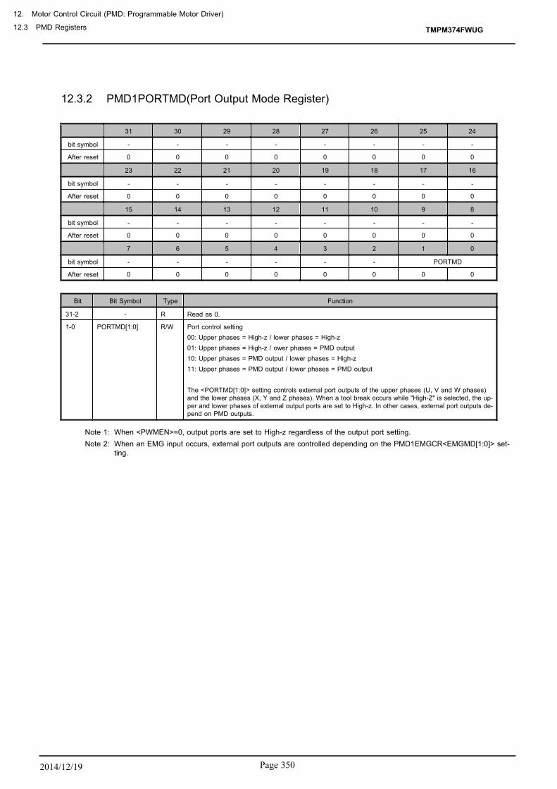
12.3.2 PMD1PORTMD(Port Output Mode Register)
31 30 29 28 27 26 25 24
bit symbol - - - - - - - -
After reset 0 0 0 0 0 0 0 0
23 22 21 20 19 18 17 16
bit symbol - - - - - - - -
After reset 0 0 0 0 0 0 0 0
15 14 13 12 11 10 9 8
bit symbol - - - - - - - -
After reset 0 0 0 0 0 0 0 0
7 6 5 4 3 2 1 0
bit symbol - - - - - - PORTMD
After reset 0 0 0 0 0 0 0 0
Bit Bit Symbol Type Function
31-2 - R Read as 0.
1-0 PORTMD[1:0] R/W Port control setting00: Upper phases = High-z / lower phases = High-z01: Upper phases = High-z / ower phases = PMD output10: Upper phases = PMD output / lower phases = High-z11: Upper phases = PMD output / lower phases = PMD output The <PORTMD[1:0]> setting controls external port outputs of the upper phases (U, V and W phases)and the lower phases (X, Y and Z phases). When a tool break occurs while "High-Z" is selected, the up-per and lower phases of external output ports are set to High-z. In other cases, external port outputs de-pend on PMD outputs.
Note 1: When <PWMEN>=0, output ports are set to High-z regardless of the output port setting.Note 2: When an EMG input occurs, external port outputs are controlled depending on the PMD1EMGCR<EMGMD[1:0]> set-
ting.
TMPM374FWUG
12. Motor Control Circuit (PMD: Programmable Motor Driver)
12.3 PMD Registers
Page 3502014/12/19

12.3.3 PMD1MODESEL (Mode Select Register)
31 30 29 28 27 26 25 24
bit symbol - - - - - - - -
After reset 0 0 0 0 0 0 0 0
23 22 21 20 19 18 17 16
bit symbol - - - - - - - -
After reset 0 0 0 0 0 0 0 0
15 14 13 12 11 10 9 8
bit symbol - - - - - - - -
After reset 0 0 0 0 0 0 0 0
7 6 5 4 3 2 1 0
bit symbol - - - - - - - MDSEL
After reset 0 0 0 0 0 0 0 0
Bit Bit Symbol Type Function
31-1 - R Read as 0.
0 MDSEL R/W Mode Select Register0: Bus mode1: VE modeThis bit selects whether to load the second buffer of each double-buffered register with the register val-ue set via the bus (bus mode) or the value supplied from the Vector Engine (VE mode). The PWM com-pare registers (PMD1CMPU,PMD1CMPV, PMD1CMPW), trigger compare registers (PMD1TRGCMP0,PMD1TRGCMP1) andPMD1 MDOUT register are double-buffered, and the second buffers are loadedin synchronization with the PMD’s internal update timing.
TMPM374FWUG
Page 351 2014/12/19

12.3.4 Pulse Width Modulation Circuit
4
Up/Down
pwmw
pwmv
pwmu
PMD1CMPV
PMD1CMPU
PMD1CMPW
=
=<
=<
=<
PMD1CNTSTA PMD1MDCR
PMD1MDPRD
Buffer
Buffer
Buffer
VECMPU
VECMPV
VECMPW
PMD1MDODSEL
Lower LimitProcessing Buffer
MDCNT read
“1”CarrierPeak
CarrierBottom
PMD Counter Status Register PMD Control Register
PWM Compare Register
PWM Control
PWM Interrupt RequestINTPWM
PWM Period Register
“1” Determined
PWMCounter
Figure 12-3 Pulse Width Modulation Circuit
The pulse width modulation circuit has a 16-bit PMD up-/down-counter and generates PWM carrier wave-forms with a resolution of 12.5 nsec at 80 MHz. The PWM carrier waveform mode can be selected frommode 0 (edge-aligned PWM, sawtooth wave modulation) and mode 1 (center-aligned PWM, triangular wavemodulation).
The PWM period extension mode (PMD1MDCR<PWMCK> = 1) is also available. When this mode is selec-ted, the PWM counter generates PWM carrier waveforms with a resolution of 50 nsec.
TMPM374FWUG
12. Motor Control Circuit (PMD: Programmable Motor Driver)
12.3 PMD Registers
Page 3522014/12/19

1. Setting the PWM period
The PWM period is determined by the PMD1MDPRD register. This register is double-buffered.Comparator input is updated at every PWM period. It is also possible to update comparator inputat every half PWM period.
PWM : register =PWM frequency [Hz]
[Hz]PMD1MDPRD
Trianguler wave PWM : register value =PWM frequency [Hz] x 2
Oscillation frequency [Hz]PMD1MDPRD
2. Compare function
The pulse width modulation circuit compares the PWM compare registers of the 3 phases(PMD1CMPU / V / W) and the carrier wave generated by the PWM counter <MDPRD[15:0]> to de-termine which is larger to generate PWM waveforms with the desired duty.
The PWM compare register of each phase has a double-buffered compare register. The PWM com-pare register value is loaded at every PWM period (when the internal counter value matches the<MDPRD[15:0]> value).
It is also possible to update the compare register at every 0.5 PWM period.
TMPM374FWUG
Page 353 2014/12/19

PWMU waveformon
off
PWMU waveformon
off
<MDCNT>
<MDCNT>
PMD1MDPRD <MDPRD[15:0]>
PMD1CMPU <CMPU[15:0]>
PMD1MDPRD <MDPRD[15:0]>
PMD1CMPU <CMPU[15:0]>
<MDCNT[15:0]> counts up to PMD1MDPRD andis cleared to "1" in the next cycle.
Figure 12-4 PWM Waveforms
TMPM374FWUG
12. Motor Control Circuit (PMD: Programmable Motor Driver)
12.3 PMD Registers
Page 3542014/12/19

3. Waveform mode
Three-phase PWM waveforms can be generated in the following two modes:
1. 3-phase independent mode:
Each of the PWM compare registers for the three phases is set independently to generate in-dependent PWM waveforms for each phase. This mode is used to generate drive waveformssuch as sinusoidal waves.
2. 3-phase common mode:
Only the U-phase PWM compare register is set to generate identical PWM waveforms forall the three phases. This mode is used for rectangular wave drive of brushless DC motors.
4. Interrupt processing
The pulse width modulation circuit generates PWM interrupt requests in synchronization withPWM waveforms. The PWM interrupt period can be set to half a PWM period, one PWM period,two PWM periods or four PWM periods.
TMPM374FWUG
Page 355 2014/12/19

12.3.4.1 PMD1MDCR (PMD Control Register)
31 30 29 28 27 26 25 24
bit symbol - - - - - - - -
After reset 0 0 0 0 0 0 0 0
23 22 21 20 19 18 17 16
bit symbol - - - - - - - -
After reset 0 0 0 0 0 0 0 0
15 14 13 12 11 10 9 8
bit symbol - - - - - - - -
After reset 0 0 0 0 0 0 0 0
7 6 5 4 3 2 1 0
bit symbol - PWMCK SYNTMD DTYMD PINT INTPRD PWMMD
After reset 0 0 0 0 0 0 0 0
Bit Bit Symbol Type Function
31-7 - R Read as 0.
6 PWMCK R/W PWM period extension mode0: Normal period1: 4x periodWhen <PWMCK>= "0", the PWM counter operates with a resolution of 12.5 ns at fsys=80 MHz.・ Sawtooth wave: 12.5 ns, triangular wave: 25 nsWhen <PWMCK>="1", the PWM counter operates with a resolution of 50 ns at fsys=80 MHz.・ Sawtooth wave: 50 ns, triangular wave: 100 ns
5 SYNTMD R/W Port output modeThis bit specifies the port output setting of the U, V and W phases. (See Table 12-2.)
4 DTYMD R/W Duty mode0: 3-phase common mode1: 3-phase independent modeThis bit selects whether to make duty setting independently for each phase or to use the PMD1CMPU reg-ister for all three phases.
3 PINT R/W PWM interrupt timing0: Interrupt request when PWM counter PMD1MDCNT<MDCNT[15:0]> = 0x00011: Interrupt request when PWM counter PMD1MDCNT<MDCNT[15:0]> = <MDPRD[15:0]>This bit selects whether to generate an interrupt request when the PWM counter equals its minimum ormaximum value. When the edge-aligned PWM mode is selected, an interrupt request is generatedwhen the PWM counter equals the <MDPRD[15:0]> value. When the PWM interrupt period is set to ev-ery 0.5 PWM period, an interrupt request is generated when the PWM counter equals "1" or <MDPRD[15:0]>.
2-1 INTPRD[1:0] R/W PWM interrupt period00: Interrupt request at every 0.5 PWM period (<PWMMD>= "1" only)01: Interrupt request at every PWM period10: Interrupt request at every 2 PWM periods11: Interrupt request at every 4 PWM periodsThis field selects the PWM interrupt period from 0.5 PWM period, one PWM period, two PWM periodsand four PWM periods.・note) When <INTPRD[1:0]>= "00", the contents of the compare registers (PMD1CMPU/V/W) and peri-od register (PMD1MDPRD) are updated into their respective buffers when the internal counter equals 1or the PMD1MDPRD value.
0 PWMMD R/W PWM carrier waveform0: PWM mode 0 (edge-aligned PWM, sawtooth wave)1: PWM mode 1(center-aligned PWM, triangular wave)This bit selects the PWM mode. PWM mode 0 is edge-aligned PWM and PWM mode 1 is center-aligned PWM.
TMPM374FWUG
12. Motor Control Circuit (PMD: Programmable Motor Driver)
12.3 PMD Registers
Page 3562014/12/19
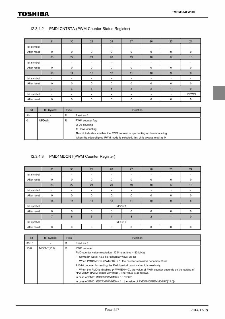
12.3.4.2 PMD1CNTSTA (PWM Counter Status Register)
31 30 29 28 27 26 25 24
bit symbol - - - - - - - -
After reset 0 0 0 0 0 0 0 0
23 22 21 20 19 18 17 16
bit symbol - - - - - - - -
After reset 0 0 0 0 0 0 0 0
15 14 13 12 11 10 9 8
bit symbol - - - - - - - -
After reset 0 0 0 0 0 0 0 0
7 6 5 4 3 2 1 0
bit symbol - - - - - - - UPDWN
After reset 0 0 0 0 0 0 0 0
Bit Bit Symbol Type Function
31-1 - R Read as 0.
0 UPDWN R PWM counter flag0: Up-counting1: Down-countingThis bit indicates whether the PWM counter is up-counting or down-counting.When the edge-aligned PWM mode is selected, this bit is always read as 0.
12.3.4.3 PMD1MDCNT(PWM Counter Register)
31 30 29 28 27 26 25 24
bit symbol - - - - - - - -
After reset 0 0 0 0 0 0 0 0
23 22 21 20 19 18 17 16
bit symbol - - - - - - - -
After reset 0 0 0 0 0 0 0 0
15 14 13 12 11 10 9 8
bit symbol MDCNT
After reset 0 0 0 0 0 0 0 0
7 6 5 4 3 2 1 0
bit symbol MDCNT
After reset 0 0 0 0 0 0 0 0
Bit Bit Symbol Type Function
31-16 - R Read as 0.
15-0 MDCNT[15:0] R PWM counterPMD counter value (resolution: 12.5 ns at fsys = 80 MHz)・ Sawtooth wave: 12.5 ns, triangular wave: 25 ns・ When PMD1MDCR<PWMCK> = 1, the counter resolution becomes 50 ns.A16-bit counter for reading the PWM period count value. It is read-only.・ When the PMD is disabled (<PWMEN>=0), the value of PWM counter depends on the setting of<PWMMD> (PWM carrier waveform). The value is as follows.In case of PMD1MDCR<PWMMD>= 0 : 0x0001In case of PMD1MDCR<PWMMD>= 1 : the value of PMD1MDPRD<MDPRD[15:0]>
TMPM374FWUG
Page 357 2014/12/19

12.3.4.4 PMD1MDPRD(PWM Period Register)
31 30 29 28 27 26 25 24
bit symbol - - - - - - - -
After reset 0 0 0 0 0 0 0 0
23 22 21 20 19 18 17 16
bit symbol - - - - - - - -
After reset 0 0 0 0 0 0 0 0
15 14 13 12 11 10 9 8
bit symbol MDPRD
After reset 0 0 0 0 0 0 0 0
7 6 5 4 3 2 1 0
bit symbol MDPRD
After reset 0 0 0 0 0 0 0 0
Bit Bit Symbol Type Function
31-16 - R Read as 0.
15-0 MDPRD[15:0] R/W PWM period<MDPRD[15:0]> ≥ 0x010A 16-bit register for specifying the PWM period. This register is double-buffered and can be changedeven when the PWM counter is operating. The buffer is loaded at every PWM period.(That is, when the PWM counter matches the <MDPRD[15:0]> value. When 0.5 PWM period is selec-ted, loading is performed when the PWM counter matches 1 or <MDPRD[15:0]>. The least significantbit must be set as 0.)If <MDPRD[15:0]> is set to a value less than 0x0010, it is automatically assumed to be 0x0010. (The reg-ister retains the actual value that is written.)
Note:Do not write to this register in byte units. If the upper 8 bits [15:8] and the lower 8 bits [7:0]are written separately, operation cannot be guaranteed.
TMPM374FWUG
12. Motor Control Circuit (PMD: Programmable Motor Driver)
12.3 PMD Registers
Page 3582014/12/19

12.3.4.5 PMD1CMPU ( PWM Compare Registers of U Phase )
31 30 29 28 27 26 25 24
bit symbol - - - - - - - -
After reset 0 0 0 0 0 0 0 0
23 22 21 20 19 18 17 16
bit symbol - - - - - - - -
After reset 0 0 0 0 0 0 0 0
15 14 13 12 11 10 9 8
bit symbol CMPU1
After reset 0 0 0 0 0 0 0 0
7 6 5 4 3 2 1 0
bit symbol CMPU1
After reset 0 0 0 0 0 0 0 0
Bit Bit Symbol Type Function
31-16 - R Read as 0.
15-0 CMPU1[15:0] R/W PWM pulse width of U PhaseCompare registers (resolution : 12.5 ns at fsys =80 MHz)・ Sawtooth wave: 12.5 ns, triangular wave: 25 ns・ When MDCR<PWMCK>="1", the counter resolution becomes 50 ns. <CMPU1[15:0]> are compare registers for determining the output pulse width of the U phases. Thesesregisters are double-buffered. Pulse width is determined by comparing the buffer and the PWM counterto evaluate which is larger. (To be loaded when the PWM counter value matches the <MDPRD[15:0]> val-ue. When 0.5 PWM period is selected, loading is performed when the PWM counter matches 1 or<MDPRD[15:0]>.)When this register is read, the value of the first buffer (data set via the bus) is returned.
Note 1: To load the second buffer with the value in the compare register updated via the bus, select the busmode (default) by setting PMD1MODESEL<MDSEL> to 0.
Note 2: Do not write to these registers in byte units. If the upper 8 bits [15:8] and the lower 8 bits [7:0] are writ-ten separately, operation cannot be guaranteed.
TMPM374FWUG
Page 359 2014/12/19
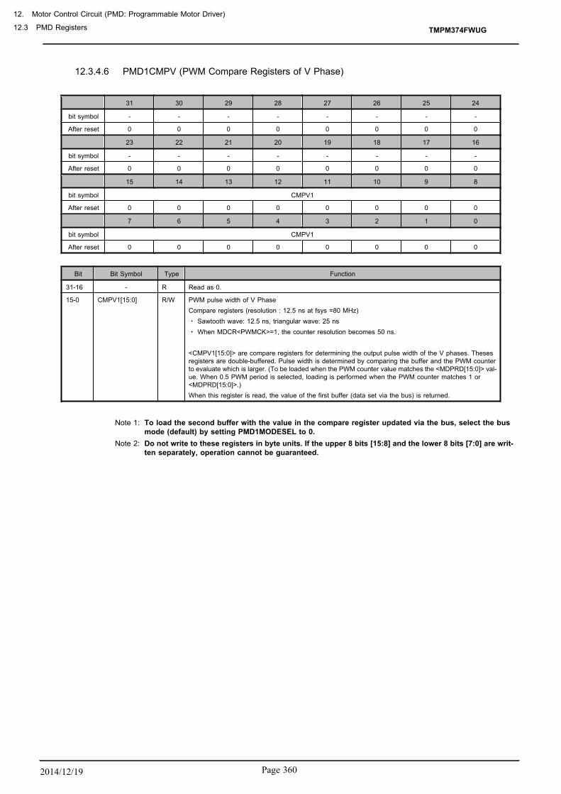
12.3.4.6 PMD1CMPV (PWM Compare Registers of V Phase)
31 30 29 28 27 26 25 24
bit symbol - - - - - - - -
After reset 0 0 0 0 0 0 0 0
23 22 21 20 19 18 17 16
bit symbol - - - - - - - -
After reset 0 0 0 0 0 0 0 0
15 14 13 12 11 10 9 8
bit symbol CMPV1
After reset 0 0 0 0 0 0 0 0
7 6 5 4 3 2 1 0
bit symbol CMPV1
After reset 0 0 0 0 0 0 0 0
Bit Bit Symbol Type Function
31-16 - R Read as 0.
15-0 CMPV1[15:0] R/W PWM pulse width of V PhaseCompare registers (resolution : 12.5 ns at fsys =80 MHz)・ Sawtooth wave: 12.5 ns, triangular wave: 25 ns・ When MDCR<PWMCK>=1, the counter resolution becomes 50 ns. <CMPV1[15:0]> are compare registers for determining the output pulse width of the V phases. Thesesregisters are double-buffered. Pulse width is determined by comparing the buffer and the PWM counterto evaluate which is larger. (To be loaded when the PWM counter value matches the <MDPRD[15:0]> val-ue. When 0.5 PWM period is selected, loading is performed when the PWM counter matches 1 or<MDPRD[15:0]>.)When this register is read, the value of the first buffer (data set via the bus) is returned.
Note 1: To load the second buffer with the value in the compare register updated via the bus, select the busmode (default) by setting PMD1MODESEL to 0.
Note 2: Do not write to these registers in byte units. If the upper 8 bits [15:8] and the lower 8 bits [7:0] are writ-ten separately, operation cannot be guaranteed.
TMPM374FWUG
12. Motor Control Circuit (PMD: Programmable Motor Driver)
12.3 PMD Registers
Page 3602014/12/19
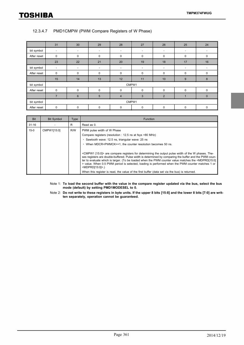
12.3.4.7 PMD1CMPW (PWM Compare Registers of W Phase)
31 30 29 28 27 26 25 24
bit symbol - - - - - - - -
After reset 0 0 0 0 0 0 0 0
23 22 21 20 19 18 17 16
bit symbol - - - - - - - -
After reset 0 0 0 0 0 0 0 0
15 14 13 12 11 10 9 8
bit symbol CMPW1
After reset 0 0 0 0 0 0 0 0
7 6 5 4 3 2 1 0
bit symbol CMPW1
After reset 0 0 0 0 0 0 0 0
Bit Bit Symbol Type Function
31-16 - R Read as 0.
15-0 CMPW1[15:0] R/W PWM pulse width of W PhaseCompare registers (resolution : 12.5 ns at fsys =80 MHz)・ Sawtooth wave: 12.5 ns, triangular wave: 25 ns・ When MDCR<PWMCK>=1, the counter resolution becomes 50 ns. <CMPW1 [15:0]> are compare registers for determining the output pulse width of the W phases. The-ses registers are double-buffered. Pulse width is determined by comparing the buffer and the PWM coun-ter to evaluate which is larger. (To be loaded when the PWM counter value matches the <MDPRD[15:0]> value. When 0.5 PWM period is selected, loading is performed when the PWM counter matches 1 or<MDPRD[15:0]>.)When this register is read, the value of the first buffer (data set via the bus) is returned.
Note 1: To load the second buffer with the value in the compare register updated via the bus, select the busmode (default) by setting PMD1MODESEL to 0.
Note 2: Do not write to these registers in byte units. If the upper 8 bits [15:8] and the lower 8 bits [7:0] are writ-ten separately, operation cannot be guaranteed.
TMPM374FWUG
Page 361 2014/12/19
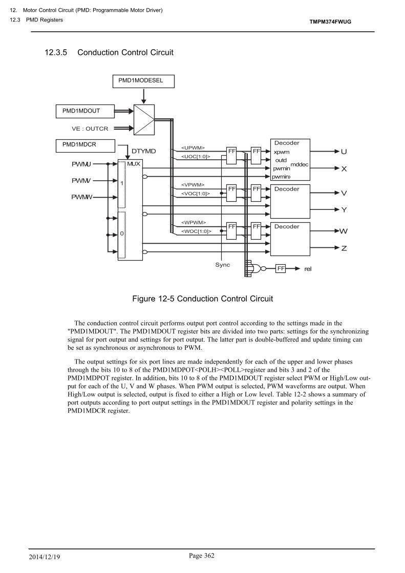
12.3.5 Conduction Control Circuit
Decoder
Decoder
Decoder
MUX PWMU
PWMV
PWMW
FF
FF
FF
DTYMD
0
1
xpwm outd
pwmin pwminx
mddec
FF rel
FF
FF
FF
Sync
VE : OUTCR
<UPWM>
<UOC[1:0]>
<VPWM>
<VOC[1:0]>
<WPWM>
<WOC[1:0]>
PMD1MODESEL
PMD1MDOUT
PMD1MDCR
Figure 12-5 Conduction Control Circuit
The conduction control circuit performs output port control according to the settings made in the"PMD1MDOUT". The PMD1MDOUT register bits are divided into two parts: settings for the synchronizingsignal for port output and settings for port output. The latter part is double-buffered and update timing canbe set as synchronous or asynchronous to PWM.
The output settings for six port lines are made independently for each of the upper and lower phasesthrough the bits 10 to 8 of the PMD1MDPOT<POLH><POLL>register and bits 3 and 2 of thePMD1MDPOT register. In addition, bits 10 to 8 of the PMD1MDOUT register select PWM or High/Low out-put for each of the U, V and W phases. When PWM output is selected, PWM waveforms are output. WhenHigh/Low output is selected, output is fixed to either a High or Low level. Table 12-2 shows a summary ofport outputs according to port output settings in the PMD1MDOUT register and polarity settings in thePMD1MDCR register.
TMPM374FWUG
12. Motor Control Circuit (PMD: Programmable Motor Driver)
12.3 PMD Registers
Page 3622014/12/19

12.3.5.1 PMD1MDPOT (PMD Output Setting Register)
31 30 29 28 27 26 25 24
bit symbol - - - - - - - -
After reset 0 0 0 0 0 0 0 0
23 22 21 20 19 18 17 16
bit symbol - - - - - - - -
After reset 0 0 0 0 0 0 0 0
15 14 13 12 11 10 9 8
bit symbol - - - - - - - -
After reset 0 0 0 0 0 0 0 0
7 6 5 4 3 2 1 0
bit symbol - - - - POLH POLL PSYNCS
After reset 0 0 0 0 0 0 0 0
Bit Bit Symbol Type Function
31-4 - R Read as 0.
3 POLH R/W Upper phase port polarity (Note)0: Active low1: Active highPOLH selects the output port polarity of the upper phases.
2 POLL R/W Lower phase port polarity (Note)0: Active low1: Active highPOLL selects the output port polarity of the lower phases.
1-0 PSYNCS[1:0] R/W MDOUT transfer timing (Note)00: Async to PWM01: Load when PWM counter <MDCNT[15:0]> = 110: Load when PWM counter <MOCNT[15:0]> = PMD1MDPRD<MDPRD[15:0]>11: Load when PWM counter <MDCNT[15:0]> = 1 or PMD1MDPRD<MDPRD[15:0]> PSYNCS selects the timing when the U-, V- and W-phase output settings are reflected in port outputs(sync or async to the PWM counter peak, bottom or peak/bottom).When "00" (Async to PWM) is selected, the changing of MDOUT register is applied to the U-, V- and W-phase output immediately. The <PSYNCS> is also available in the vector engine.
Note:This field must be set while PMD1MDEN<PWMEN>=0.
TMPM374FWUG
Page 363 2014/12/19

12.3.5.2 PMD1MDOUT(PMD Output Control Register)
31 30 29 28 27 26 25 24
bit symbol - - - - - - - -
After reset 0 0 0 0 0 0 0 0
23 22 21 20 19 18 17 16
bit symbol - - - - - - - -
After reset 0 0 0 0 0 0 0 0
15 14 13 12 11 10 9 8
bit symbol - - - - - WPWM VPWM UPWM
After reset 0 0 0 0 0 0 0 0
7 6 5 4 3 2 1 0
bit symbol - - WOC VOC UOC
After reset 0 0 0 0 0 0 0 0
Bit Bit Symbol Type Function
31-11 - R Read as 0.
10 WPWM R/W U-, V-, and W-phase output control0: High/Low Output1: PWM OutputThe MDOUT register controls the port outputs of the U, V and W phases (see Table 12-2 below.)
9 VPWM R/W
8 UPWM R/W
7-6 - R Read as 0.
5-4 WOC[1:0] R/W U-, V-, and W-phase output controlThe MDOUT register controls the port outputs of the U, V and W phases (see Table 12-2below.)3-2 VOC[1:0] R/W
1-0 UOC[1:0] R/W
Note 1: To load the second buffer of PWM1 MDOUT with a value updated via the bus, select the bus mode (de-fault) by setting PMD1MODESEL to 0.
Note 2: Do not write to this register in byte units. If the upper 8 bits [15:8] and the lower 8 bits [7:0] are writ-ten separately, operation cannot be guaranteed.
TMPM374FWUG
12. Motor Control Circuit (PMD: Programmable Motor Driver)
12.3 PMD Registers
Page 3642014/12/19

Table 12-2 Port Outputs according to the <UOC>, <VOC>, <WOC>, <UPWM>, <VPWM> and <WPWM>Settings
PMD1MDCR<SYNTMD>=0 PMD1MDCR<SYNTMD>=0
Polarity: Active high (PMD1MDPOT<POLH><POLL>="11") Polarity: Active low (PMD1MDPOT<POLH><POLL>="00")
PMD1MDOUTOutput Control <WPWM><VPWM><UPWM>
Output Select
PMD1MDOUTOutput Control <WPWM><VPWM><UPWM>
Output Select(Upperphase)
(Lowerphase) (Upper
phase)(Lowerphase)
<WOC[1]><VOC[1]><UOC[1]>
<WOC[0]><VOC[0]
><UOC[0]>
0: H/L output 1: PWM output <WOC[1]><VOC[1]><UOC[1]>
<WOC[0]><VOC[0]
><UOC[0]>
0: H/L output 1: PWM output
Upperphaseoutput
Lowerphaseoutput
Upperphaseoutput
Lowerphaseoutput
Upperphaseoutput
Lowerphaseoutput
Upperphaseoutput
Lowerphaseoutput
0 0 L L PWM PWM 0 0 H H PWM PWM
0 1 L H L PWM 0 1 H L H PWM
1 0 H L PWM L 1 0 L H PWM H
1 1 H H PWM PWM 1 1 L L PWM PWM
PMD1MDCR<SYNTMD>=1 PMD1MDCR<SYNTMD>=1
Polarity: Active high (PMD1MDPOT<POLH><POLL>="11") Polarity: Active low (PMD1MDPOT<POLH><POLL>="00")
PMD1MDOUTOutput Control <WPWM><VPWM><UPWM>
Output Select
PMD1MDOUTOutput Control <WPWM><VPWM><UPWM>
Output Select(Upperphase)
(Lowerphase) (Upper
phase)(Lowerphase)
<WOC[1]><VOC[1]><UOC[1]>
<WOC[0]><VOC[0]
><UOC[0]>
0: H/L output 1: PWM output <WOC[1]><VOC[1]><UOC[1]>
<WOC[0]><VOC[0]
><UOC[0]>
0: H/L output 1: PWM output
Upperphaseoutput
Lowerphaseoutput
Upperphaseoutput
Lowerphaseoutput
Upperphaseoutput
Lowerphaseoutput
Upperphaseoutput
Lowerphaseoutput
0 0 L L PWM PWM 0 0 H H PWM PWM
0 1 L H L PWM 0 1 H L H PWM
1 0 H L PWM L 1 0 L H PWM H
1 1 H H PWM PWM 1 1 L L PWM PWM
・ Output Settings for One-Shunt MODE
One-Shunt can be supported by the following settings.
Table 12-3 Register Settings for One-Shunt
Normal PWM center on U-Phase PWM center off V-Phase PWM center off W-Phase PWM center off
CMPU duty_U <MDPRD[15:0]>-duty_U duty_U duty_U
CMPV duty_V duty_V <MDPRD[15:0]>-duty_V duty_V
CMPW duty_W duty_W duty_W <MDPRD[15:0]>-duty_W
<UOC[1:0]> 11 00 11 11
<VOC[1:0]> 11 11 00 11
<WOC[1:0]> 11 11 11 00
TMPM374FWUG
Page 365 2014/12/19

12.3.6 Protection Control Circuit
Protection Control
U
X
V
Y
W
u‘
Z
x‘
v‘
y‘
w‘
z‘
PTEN_N Lower phase output enable
<EMGST> EMG port input enableINTEMG EMG interruptEMG EMG input
EMG Release Register
EMG Controi Register
PTENC
OVV Control Register
INTOVV OVV interruptOVV OVV input
PTEN_P Upper phase output enable
PMD1EMGCR PMD1EMGRELPMD1OVVCR
Figure 12-6 Protection Control Circuit
The protection control circuit consists of an EMG protection control circuit and an OVV protection con-trol circuit.
TMPM374FWUG
12. Motor Control Circuit (PMD: Programmable Motor Driver)
12.3 PMD Registers
Page 3662014/12/19

12.3.6.1 EMG Protection Circuit
The EMG protection circuit consists of an EMG protection control unit and a port output disable unit.This circuit is activated when the EMG input becomes low.
The EMG protection circuit offers an emergency stop mechanism: when the EMG input is asserted(H→L), all six port outputs are immediately disabled (depending on the PMD1EMGCR<EMGMD> set-ting) and an EMG interrupt (INTEMG) is generated. <EMGMD> can be set to output a control signalthat sets external output ports to High-z in case of an emergency.
A tool break also disables all six PWM output lines depending on the PMD1PORTMD<PORTMD> set-ting. When a tool break occurs, external output ports can be set to High-z through the setting of thePMD1EMGSTA<EMGST> register.
EMG protection is set through the EMG Control Register (PMD1EMGCR).
A read value of 1 in EMGSTA<EMGST> indicates that the EMG protection circuit is active. In thisstate, EMG protection can be released by setting all the port output lines inactive (PMD1MDOUT<[10:8]><[5:0]>) and then setting EMGCR<EMGRS> to 1. To disable the EMG protection function, write"0x5A" and "0xA5" in this order to the EMGREL register and then clear EMGCR<EMGEN> to 0.(These three instructions must be executed consecutively.) While the EMG protection input is low, any at-tempt to release the EMG protection state is ignored. Before setting PMD1MGCR<EMGRS> to 1 to re-lease EMG protection, make sure that PMD1EMGST<EMGI> is high.
The EMG protection circuit can be disabled only after the specified key codes ("0x5A", "0xA5") are writ-ten in the <EMGREL> register to prevent it from being inadvertently disabled.
Note: Initial procedure for EMG function
After reset, the EMG function is enabled but EMG pin is configured as a normal port. Therefore, as the EMG protec-tion might be valid, release the EMG protection by the following procedure at the initial sequence.
1: Selects EMG function by PxFR register.
2: Reads PMD1EMGSTA<EMGI> to confirm it as "1".
3: Sets PMD1MDOUT<[10:8]>, <[5:0]> to "0" to make all ports in-active ("L" output).
4: Releases EMG protection by setting PMD1EMGCR<EMGRS> to "1".
If the EMG protection is to be disabled, continue the following procedure.
5: Writes the key codes to PMD1EMGREL (In order of "0x5A" and "0xA5")
6: Sets PMD1EMGCR<EMGEN> to "0" to disable the EMG protection.
TMPM374FWUG
Page 367 2014/12/19

12.3.6.2 PMD1EMGREL (EMG Release Register)
31 30 29 28 27 26 25 24
bit symbol - - - - - - - -
After reset 0 0 0 0 0 0 0 0
23 22 21 20 19 18 17 16
bit symbol - - - - - - - -
After reset 0 0 0 0 0 0 0 0
15 14 13 12 11 10 9 8
bit symbol - - - - - - - -
After reset 0 0 0 0 0 0 0 0
7 6 5 4 3 2 1 0
bit symbol EMGREL
After reset 0 0 0 0 0 0 0 0
Bit Bit Symbol Type Function
31-8 - R Read as 0.
7-0 EMGREL[7:0] W EMG disable codeThe EMG and OVV protection functions can be disabled by setting 0x5A and 0xA5 in this order to bits7 to 0 of the <EMGREL[7:0]> register.When disabling these functions, <EMGEN> and <OVVEN> must be cleared to "0".・ This register is used for both the EMG and OVV functions.
TMPM374FWUG
12. Motor Control Circuit (PMD: Programmable Motor Driver)
12.3 PMD Registers
Page 3682014/12/19
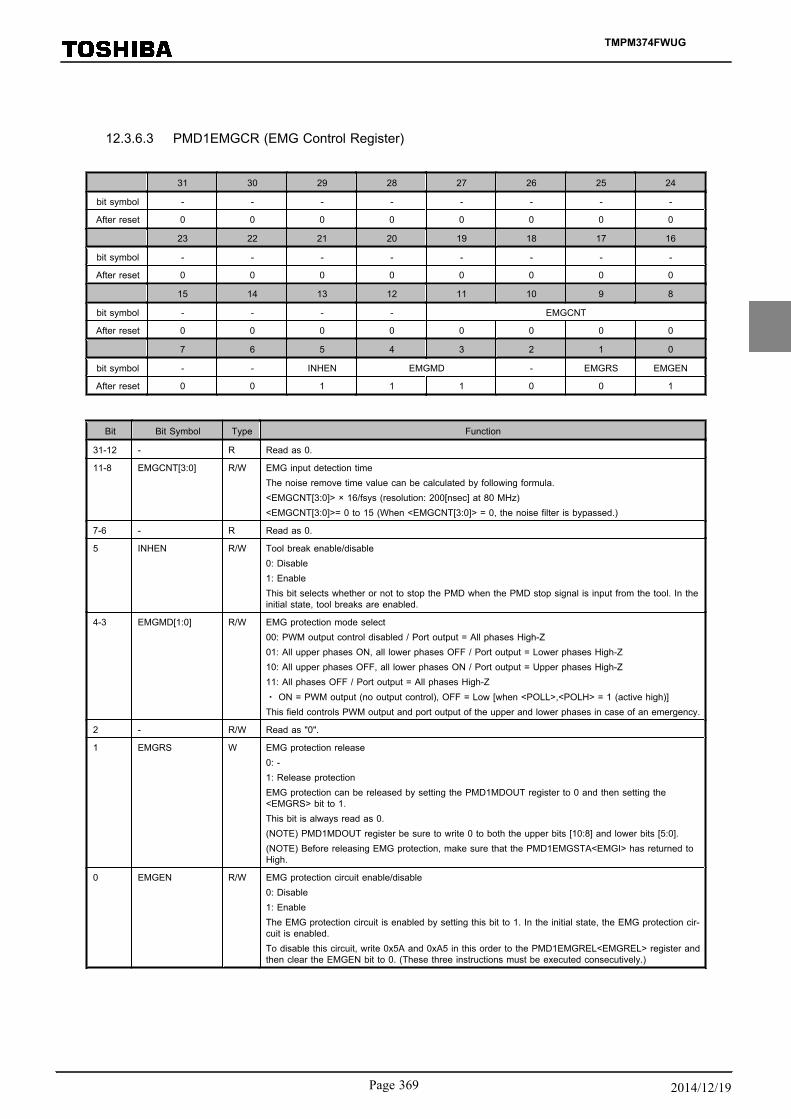
12.3.6.3 PMD1EMGCR (EMG Control Register)
31 30 29 28 27 26 25 24
bit symbol - - - - - - - -
After reset 0 0 0 0 0 0 0 0
23 22 21 20 19 18 17 16
bit symbol - - - - - - - -
After reset 0 0 0 0 0 0 0 0
15 14 13 12 11 10 9 8
bit symbol - - - - EMGCNT
After reset 0 0 0 0 0 0 0 0
7 6 5 4 3 2 1 0
bit symbol - - INHEN EMGMD - EMGRS EMGEN
After reset 0 0 1 1 1 0 0 1
Bit Bit Symbol Type Function
31-12 - R Read as 0.
11-8 EMGCNT[3:0] R/W EMG input detection timeThe noise remove time value can be calculated by following formula.<EMGCNT[3:0]> × 16/fsys (resolution: 200[nsec] at 80 MHz)<EMGCNT[3:0]>= 0 to 15 (When <EMGCNT[3:0]> = 0, the noise filter is bypassed.)
7-6 - R Read as 0.
5 INHEN R/W Tool break enable/disable0: Disable1: EnableThis bit selects whether or not to stop the PMD when the PMD stop signal is input from the tool. In theinitial state, tool breaks are enabled.
4-3 EMGMD[1:0] R/W EMG protection mode select00: PWM output control disabled / Port output = All phases High-Z01: All upper phases ON, all lower phases OFF / Port output = Lower phases High-Z10: All upper phases OFF, all lower phases ON / Port output = Upper phases High-Z11: All phases OFF / Port output = All phases High-Z・ ON = PWM output (no output control), OFF = Low [when <POLL>,<POLH> = 1 (active high)]This field controls PWM output and port output of the upper and lower phases in case of an emergency.
2 - R/W Read as "0".
1 EMGRS W EMG protection release0: -1: Release protectionEMG protection can be released by setting the PMD1MDOUT register to 0 and then setting the<EMGRS> bit to 1.This bit is always read as 0.(ΝΟΤΕ) PMD1MDOUT register be sure to write 0 to both the upper bits [10:8] and lower bits [5:0].(ΝΟΤΕ) Before releasing EMG protection, make sure that the PMD1EMGSTA<EMGI> has returned toHigh.
0 EMGEN R/W EMG protection circuit enable/disable0: Disable1: EnableThe EMG protection circuit is enabled by setting this bit to 1. In the initial state, the EMG protection cir-cuit is enabled.To disable this circuit, write 0x5A and 0xA5 in this order to the PMD1EMGREL<EMGREL> register andthen clear the EMGEN bit to 0. (These three instructions must be executed consecutively.)
TMPM374FWUG
Page 369 2014/12/19
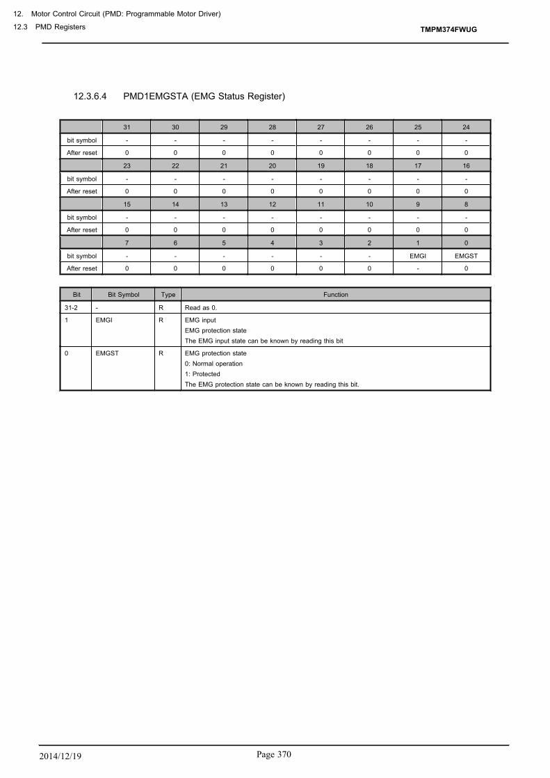
12.3.6.4 PMD1EMGSTA (EMG Status Register)
31 30 29 28 27 26 25 24
bit symbol - - - - - - - -
After reset 0 0 0 0 0 0 0 0
23 22 21 20 19 18 17 16
bit symbol - - - - - - - -
After reset 0 0 0 0 0 0 0 0
15 14 13 12 11 10 9 8
bit symbol - - - - - - - -
After reset 0 0 0 0 0 0 0 0
7 6 5 4 3 2 1 0
bit symbol - - - - - - EMGI EMGST
After reset 0 0 0 0 0 0 - 0
Bit Bit Symbol Type Function
31-2 - R Read as 0.
1 EMGI R EMG inputEMG protection stateThe EMG input state can be known by reading this bit
0 EMGST R EMG protection state0: Normal operation1: ProtectedThe EMG protection state can be known by reading this bit.
TMPM374FWUG
12. Motor Control Circuit (PMD: Programmable Motor Driver)
12.3 PMD Registers
Page 3702014/12/19

12.3.6.5 OVV Protection Control Circuit (OVV Block)
The OVV protection control circuit consists of an OVV protection control unit and a port output disa-ble unit. This circuit is activated when the OVV input port is asserted.
When the OVV input is asserted (H→L) for a specified period (set in OVVCR<OVVCNT>), the OVVprotection circuit fixes the six port output lines in the conduction control circuit to high or low. At thistime, an OVV interrupt (INTOVV) is generated.
It is possible to turn off only the upper or lower phases or all phases.
OVV protection is set through the "PMD1OVVCR". A read value of "1" in PMD1OVV-STA<OVVST> indicates that the OVV protection circuit is active.
The release of the OVV protection state is enabled by setting PMD1OVVCR<OVVRS> to "1". Then,OVV protection is automatically released after the OVV protection circuit completes its operation.
( The OVV protection state is not released while the OVV protection input is low. The state of thisport input can be checked by reading PMD1OVVSTA<OVVI>. )
The OVV protection state is released in synchronization with the PWM period (when the PWM countmatches the <MDPRD[15:0]> value. When 0.5 PWM period is selected, the release timing is when thePWM counter equals 1 or <MDPRD[15:0]>.). To disable the OVV protection function, write "0x5A" and"0xA5" in this order to the <EMGREL[7:0]> and then clear PMD1OVVCR<OVVEN> to 0. (These threeinstructions must be executed consecutively.)
The OVV protection circuit can be disabled only after the specified key codes ("0x5A", "0xA5") are writ-ten in the <EMGREL[7:0]> register to prevent it from being inadvertently disabled.
TMPM374FWUG
Page 371 2014/12/19

12.3.6.6 PMD1OVVCR (OVV Control Register)
31 30 29 28 27 26 25 24
bit symbol - - - - - - - -
After reset 0 0 0 0 0 0 0 0
23 22 21 20 19 18 17 16
bit symbol - - - - - - - -
After reset 0 0 0 0 0 0 0 0
15 14 13 12 11 10 9 8
bit symbol - - - - OVVCNT
After reset 0 0 0 0 0 0 0 0
7 6 5 4 3 2 1 0
bit symbol - ADIN1EN ADIN0EN OVVMD OVVISEL OVVRS OVVEN
After reset 0 0 0 0 0 0 0 0
Bit Bit Symbol Type Function
31-12 - R Read as 0.
11-8 OVVCNT[3:0] R/W OVV input detection timeOVVCNT = 1 to 15 (If 0 is set, it is handled as 1.)OVVCNT × 16/fsys (resolution: 200[nsec] at 80 MHz ) (NOTE) OVVCNT is effective only when port input is selected as the OVV signal (<OVVISEL> = "1").
7 - R Read as 0.
6 ADIN1EN R/W ADC B monitor interrupt input enable0: Disable input1: Enable inputThis bit selects whether to enable or disable the monitor signal input from ADC B.When this bit is set to enable and <OVVISEL>="1", the PMD is placed in a protection state (if OVV pro-tection is enabled) by an interrupt signal from ADC B that is generated by a match between an AD con-version result and the specified compare value.・ For details, refer to the chapter on "AD Conversion Monitoring Function."
5 ADIN0EN R/W ADC A monitor interrupt input enable0: Disable1: EnableThis bit selects whether to enable or disable the monitor signal input from ADC A.When this bit is set to enable and <OVVISEL>="1", the PMD is placed in a protection state (if OVV pro-tection is enabled) by an interrupt signal from ADC A that is generated by a match between an AD con-version result and the specified compare value.・ For details, refer to the chapter on "AD Conversion Monitoring Function."
4-3 OVVMD[1:0] R/W OVV protection mode00: No output control01: All upper phases ON, all lower phases OFF10: All upper phases OFF, all lower phases ON11: All phases OFF (ON = High, OFF = Low [when <POLL>,<POLH> = 1 (active high)])This field controls the outputs of the upper and lower phases when an OVV condition occurs. (NOTE) If OVV and EMG conditions occur simultaneously, the protection mode settings in the <EMGMD[1:0]> register become effective.
2 OVVISEL R/W OVV input select0: Port input1: ADC monitor signalThis bit selects whether to use port input or the monitor signal from the ADC as the OVV signal to be in-put to the protection circuit. (NOTE) When the ADC monitor signal is selected, <OVVCNT[3:0]> becomes invalid.
TMPM374FWUG
12. Motor Control Circuit (PMD: Programmable Motor Driver)
12.3 PMD Registers
Page 3722014/12/19

Bit Bit Symbol Type Function
1 OVVRS R/W OVV protection release0: Disable automatic release of OVV protection1: Enable automatic release of OVV protectionThe OVV protection state is entered when the overvoltage detection signal makes a High-to-low transi-tion. After the overvoltage detection signal returns high, the OVV protection state can be automatically re-leased by a match between the PWM counter and the <MDPRD[15:0]>) register by setting this bit to "1". (NOTE) When 0.5 PWM period is selected (PMD1MDCR<INTPRD[1:0]> = "00"), the OVV protectionstate is released when the PWM counter equals "1" or <MDPRD[15:0]> .
0 OVVEN R/W OVV protection circuit enable/disable0: Disable1: EnableThe OVV protection circuit is enabled by setting this bit to 1. In the initial state, the OVV protection cir-cuit is disabled.To disable this circuit, write "0x5A" and "0xA5" in this order to the <EMGREL[7:0]> register and thenclear <OVVEN> bit to "0". (These three instructions must be executed consecutively.)
TMPM374FWUG
Page 373 2014/12/19

12.3.6.7 PMD1OVVSTA (OVV Status Register)
31 30 29 28 27 26 25 24
bit symbol - - - - - - - -
After reset 0 0 0 0 0 0 0 0
23 22 21 20 19 18 17 16
bit symbol - - - - - - - -
After reset 0 0 0 0 0 0 0 0
15 14 13 12 11 10 9 8
bit symbol - - - - - - - -
After reset 0 0 0 0 0 0 0 0
7 6 5 4 3 2 1 0
bit symbol - - - - - - OVVI OVVST
After reset 0 0 0 0 0 0 - 0
Bit Bit Symbol Type Function
31-2 - R Read as 0.
1 OVVI R OVVI inputOVVI stateThe OVV input state (selected by OVVCR<OVVISEL>) can be known by reading this bit.
0 OVVST R OVV protection state0: Normal operation1: ProtectedThe OVV state can be known by reading this bit.
TMPM374FWUG
12. Motor Control Circuit (PMD: Programmable Motor Driver)
12.3 PMD Registers
Page 3742014/12/19

12.3.7 Dead Time Circuit
ON Delay Circuit
ON Delay Circuit
ON Delay Circuit
x‘u‘
y‘v‘
z‘w‘
X
U
Y
V
Z
W
<POLH> <POLL>
fsys/8
PMD1DTR
PMD1MDPOT PMD1MDPOT
Figure 12-7 Dead Time Circuit
The dead time circuit consists of a dead time unit and an output polarity switching unit.
For each of the U, V and W phases, the ON delay circuit introduces a delay (dead time) when the upperand lower phases are switched to prevent a short circuit. The dead time is set to the Dead Time Register(PMD1DTR<DTR[7:0]>)as an 8-bit value with a resolution of 100 ns at 80 MHz.
The output polarity switching circuit allows the polarity (active high or active low) of the upper and lowerphases to be independently set through PMD1MDPOT<POLH> and <POLL>.
TMPM374FWUG
Page 375 2014/12/19

12.3.7.1 PMD1DTR (Dead Time Register )
31 30 29 28 27 26 25 24
bit symbol - - - - - - - -
After reset 0 0 0 0 0 0 0 0
23 22 21 20 19 18 17 16
bit symbol - - - - - - - -
After reset 0 0 0 0 0 0 0 0
15 14 13 12 11 10 9 8
bit symbol - - - - - - - -
After reset 0 0 0 0 0 0 0 0
7 6 5 4 3 2 1 0
bit symbol DTR
After reset 0 0 0 0 0 0 0 0
Bit Bit Symbol Type Function
31-8 - R Read as 0.
7-0 DTR[7:0] R/W Dead timeThe Dead time value can be calculated by following formula.100 nsec × <DTR[7:0]> (up to 25.5 μsec at fsys = 80 MHz)
Note:Do not change <DTR[7:0]> register while PMD1MDEN<PWMEN> = 1.
TMPM374FWUG
12. Motor Control Circuit (PMD: Programmable Motor Driver)
12.3 PMD Registers
Page 3762014/12/19

12.3.8 Sync Trigger Generation Circuit
Buffer
BufferA=B
A=B TRG1
TRG0Slope SelectPMDTRG0
PMDTRG1
up down PTENCPWM Sync Signal
Trigger Output Select
A=B
A=B
VE : VTRGCMP0
VE : VTRGCMP1
Buffer
Buffer
TRG2
TRG3
Sector Infomation
PMDTRG2
PMDTRG3
PMDTRG4
PMDTRG5
PWM Sync Signal
PMD CounterPMD1MODSEL
PMD1TRGCMP0
PMD1TRGCMP1
PMD1TRGCMP2
PMD1TRGCMP3
PMD1TRGCR PMD1TRGMD
PMD1MDCNT
Figure 12-8 Sync Trigger Generation Circuit
The sync trigger generation circuit generates trigger signals for starting ADC sampling in synchronizationwith PWM. The ADC trigger signal (PMDTRG) is generated by a match between PMD1MDCNT andPMD1TRGCMP. The signal generation timing can be selected from up-count match, down-count match andup-/down-count match. When the edge-aligned PWM mode is selected, the ADC trigger signal is generatedon an up-count match. When PWM output is disabled (PMD1MDEN<PWMEN> = 0), trigger output is also dis-abled.
When the trigger select output mode is selected, the trigger output port is switched according to thePMD1TRGSEL<TRGSEL> register setting or sector information from the Vector Engine.
TMPM374FWUG
Page 377 2014/12/19
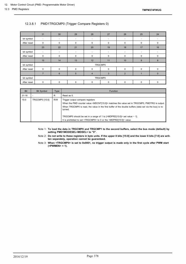
12.3.8.1 PMD1TRGCMP0 (Trigger Compare Registers 0)
31 30 29 28 27 26 25 24
bit symbol - - - - - - - -
After reset 0 0 0 0 0 0 0 0
23 22 21 20 19 18 17 16
bit symbol - - - - - - - -
After reset 0 0 0 0 0 0 0 0
15 14 13 12 11 10 9 8
bit symbol TRGCMP0
After reset 0 0 0 0 0 0 0 0
7 6 5 4 3 2 1 0
bit symbol TRGCMP0
After reset 0 0 0 0 0 0 0 0
Bit Bit Symbol Type Function
31-16 - R Read as 0.
15-0 TRGCMP0 [15:0] R/W Trigger output compare registersWhen the PMD counter value <MDCNT[15:0]> matches the value set in TRGCMP0, PMDTRG is output.When TRGCMP0 is read, the value in the first buffer of the double buffers (data set via the bus) is re-turned. TRGCMP0 should be set in a range of 1 to [<MDPRD[15:0]> set value − 1].It is prohibited to set <TRGCMP0> to 0 or the <MDPRD[15:0]> value.
Note 1: To load the data in TRGCMP0 and TRGCMP1 to the second buffers, select the bus mode (default) bysetting PMD1MODESEL<MDSEL> to "0".
Note 2: Do not write to these registers in byte units. If the upper 8 bits [15:8] and the lower 8 bits [7:0] are writ-ten separately, operation cannot be guaranteed.
Note 3: When <TRGCMP0> is set to 0x0001, no trigger output is made only in the first cycle after PWM start(<PWMEN> = 1).
TMPM374FWUG
12. Motor Control Circuit (PMD: Programmable Motor Driver)
12.3 PMD Registers
Page 3782014/12/19

12.3.8.2 PMD1TRGCMP1 (Trigger Compare Registers1)
31 30 29 28 27 26 25 24
bit symbol - - - - - - - -
After reset 0 0 0 0 0 0 0 0
23 22 21 20 19 18 17 16
bit symbol - - - - - - - -
After reset 0 0 0 0 0 0 0 0
15 14 13 12 11 10 9 8
bit symbol TRGCMP1
After reset 0 0 0 0 0 0 0 0
7 6 5 4 3 2 1 0
bit symbol TRGCMP1
After reset 0 0 0 0 0 0 0 0
Bit Bit Symbol Type Function
31-16 - R Read as 0.
15-0 TRGCMP1 [15:0] R/W Trigger output compare registersWhen the PMD counter value <MDCNT[15:0]> matches the value set in TRGCMP1, PMDTRG is output.When TRGCMP1 is read, the value in the first buffer of the double buffers (data set via the bus) is re-turned. TRGCMP1 should be set in a range of 1 to [<MDPRD[15:0]> set value = 1].It is prohibited to set <TRGCMP1> to 0 or the <MDPRD[15:0]> value.
Note 1: To load the data in TRGCMP0 and TRGCMP1 to the second buffers, select the bus mode (default) bysetting MODESEL PMD1MODESEL<MDSEL> to 0.
Note 2: Do not write to these registers in byte units. If the upper 8 bits [15:8] and the lower 8 bits [7:0] are writ-ten separately, operation cannot be guaranteed.
Note 3: When <TRGCMP1> is set to 0x0001, no trigger output is made only in the first cycle after PWM start(MDEN<PWMEN> = 1).
TMPM374FWUG
Page 379 2014/12/19

12.3.8.3 PMD1TRGCMP2 (Trigger Compare Registers 2)
31 30 29 28 27 26 25 24
bit symbol - - - - - - - -
After reset 0 0 0 0 0 0 0 0
23 22 21 20 19 18 17 16
bit symbol - - - - - - - -
After reset 0 0 0 0 0 0 0 0
15 14 13 12 11 10 9 8
bit symbol TRGCMP2
After reset 0 0 0 0 0 0 0 0
7 6 5 4 3 2 1 0
bit symbol TRGCMP2
After reset 0 0 0 0 0 0 0 0
Bit Bit Symbol Type Function
31-16 - R Read as 0.
15-0 TRGCMP2 [15:0] R/W Trigger output compare registersWhen the PMD counter value <MDCNT[15:0]> matches the value set in TRGCMP2, PMDTRG is output.When TRGCMP2 is read, the value in the first buffer of the double buffers (data set via the bus) is re-turned. TRGCMP2 should be set in a range of 1 to [<MDPRD[15:0]> set value − 1].It is prohibited to set <TRGCMP2> to 0 or the <MDPRD[15:0]> value.
Note 1: Do not write to these registers in byte units. If the upper 8 bits [15:8] and the lower 8 bits [7:0] are writ-ten separately, operation cannot be guaranteed.
Note 2: When <TRGCMP2> is set to "0x0001", no trigger output is made only in the first cycle after PWMstart (MDEN<PWMEN> = "1").
TMPM374FWUG
12. Motor Control Circuit (PMD: Programmable Motor Driver)
12.3 PMD Registers
Page 3802014/12/19
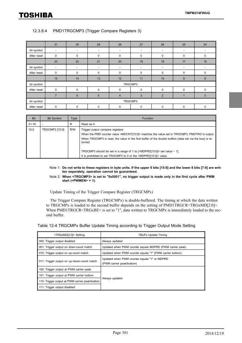
12.3.8.4 PMD1TRGCMP3 (Trigger Compare Registers 3)
31 30 29 28 27 26 25 24
bit symbol - - - - - - - -
After reset 0 0 0 0 0 0 0 0
23 22 21 20 19 18 17 16
bit symbol - - - - - - - -
After reset 0 0 0 0 0 0 0 0
15 14 13 12 11 10 9 8
bit symbol TRGCMP3
After reset 0 0 0 0 0 0 0 0
7 6 5 4 3 2 1 0
bit symbol TRGCMP3
After reset 0 0 0 0 0 0 0 0
Bit Bit Symbol Type Function
31-16 - R Read as 0.
15-0 TRGCMP3 [15:0] R/W Trigger output compare registersWhen the PMD counter value <MDCNT[15:0]> matches the value set in TRGCMP3, PMDTRG is output.When TRGCMP3 is read, the value in the first buffer of the double buffers (data set via the bus) is re-turned. TRGCMP3 should be set in a range of 1 to [<MDPRD[15:0]> set value − 1].It is prohibited to set TRGCMP3 to 0 or the <MDPRD[15:0]> value.
Note 1: Do not write to these registers in byte units. If the upper 8 bits [15:8] and the lower 8 bits [7:0] are writ-ten separately, operation cannot be guaranteed.
Note 2: When <TRGCMP3> is set to "0x0001", no trigger output is made only in the first cycle after PWMstart (<PWMEN> = 1).
Update Timing of the Trigger Compare Register (TRGCMPx)
The Trigger Compare Register (TRGCMPx) is double-buffered. The timing at which the data writtento TRGCMPx is loaded to the second buffer depends on the setting of PMD1TRGCR<TRGxMD[2:0]>.When PMD1TRGCR<TRGxBE> is set to "1", data written to TRGCMPx is immediately loaded to the sec-ond buffer.
Table 12-4 TRGCMPx Buffer Update Timing according to Trigger Output Mode Setting
<TRGxMD[2:0]> Setting TBUFx Update Timing
000: Trigger output disabled Always updated
001: Trigger output on down-count match Updated when PWM counter equals MDPRD (PWM carrier peak)
010: Trigger output on up-count match Updated when PWM counter equals "1" (PWM carrier bottom)
011: Trigger output on up-/down-count matchUpdated when PWM counter equals "1" or MDPRD(PWM carrier peak/bottom)
100: Trigger output at PWM carrier peak
Always updated101: Trigger output at PWM carrier bottom
110: Trigger output at PWM carrier peak/bottom
111: Trigger output disabled
TMPM374FWUG
Page 381 2014/12/19

12.3.8.5 PMD1TRGCR (Trigger Control Register )
31 30 29 28 27 26 25 24
bit symbol - - - - - - - -
After reset 0 0 0 0 0 0 0 0
23 22 21 20 19 18 17 16
bit symbol - - - - - - - -
After reset 0 0 0 0 0 0 0 0
15 14 13 12 11 10 9 8
bit symbol TRG3BE TRG3MD TRG2BE TRG2MD
After reset 0 0 0 0 0 0 0 0
7 6 5 4 3 2 1 0
bit symbol TRG1BE TRG1MD TRG0BE TRG0MD
After reset 0 0 0 0 0 0 0 0
Bit Bit Symbol Type Function
31-16 - R Read as 0.
15 TRG3BE R/W PMDTRG3 buffer update timing0: Sync1: Async (The value written to PMDTRG3 is immediately reflected.)This bit enables asynchronous updating of the PMDTRG3 buffers.
14-12 TRG3MD[2:0] R/W PMDTRG3 mode setting000: Trigger output disabled001: Trigger output at down-count match010: Trigger output at up-count match011: Trigger output at up-/down-count match100: Trigger output at PWM carrier peak101: Trigger output at PWM carrier bottom110: Trigger output at PWM carrier peak/bottom111: Trigger output disabledThis register selects trigger output timing.When the PMD1MDCR<PMDMD> is set to the edge-aligned mode, trigger outputs are made on up-count match or at PWM carrier peak even if down-count match or PWM carrier bottom is selected. ・ When <TRG3MD[2:0]>="011", PMD1TRGCMP3="0x0001" and PMD1MDCR<PWMMD>="1" (triangu-lar wave), one trigger output is made per period.
11 TRG2BE R/W PMDTRG2 buffer update timing0: Sync1: Async (The value written to PMDTRG2 is immediately reflected.)This bit enables asynchronous updating of the PMDTRG2 buffers.
10-8 TRG2MD[2:0] R/W PMDTRG2 mode setting000: Trigger output disabled001: Trigger output at down-count match010: Trigger output at up-count match011: Trigger output at up-/down-count match100: Trigger output at PWM carrier peak101: Trigger output at PWM carrier bottom110: Trigger output at PWM carrier peak/bottom111: Trigger output disabledThis register selects trigger output timing.When the PMD1MDCR<PMDMD> is set to the edge-aligned mode, trigger outputs are made on up-count match or at PWM carrier peak even if down-count match or PWM carrier bottom is selected. ・ When <TRG2MD[2:0]>="011", PMD1TRGCMP2="0x0001" and PMD1MDCR<PWMMD>="1" (triangu-lar wave), one trigger output is made per period.
TMPM374FWUG
12. Motor Control Circuit (PMD: Programmable Motor Driver)
12.3 PMD Registers
Page 3822014/12/19

Bit Bit Symbol Type Function
7 TRG1BE R/W PMDTRG1 buffer update timing0: Sync1: Async (The value written to PMDTRG1 is immediately reflected.)This bit enables asynchronous updating of the PMDTRG1 buffers.
6-4 TRG1MD[2:0] R/W PMDTRG1 mode setting000: Trigger output disabled001: Trigger output at down-count match010: Trigger output at up-count match011: Trigger output at up-/down-count match100: Trigger output at PWM carrier peak101: Trigger output at PWM carrier bottom110: Trigger output at PWM carrier peak/bottom111: Trigger output disabledThis register selects trigger output timing.When the PMD1MDCR<PMDMD> is set to the edge-aligned mode, trigger outputs are made on up-count match or at PWM carrier peak even if down-count match or PWM carrier bottom is selected. ・ When <TRG1MD[2:0]>="011", PMD1TRGCMP1="0x0001" and PMD1MDCR<PWMMD>="1" (triangu-lar wave), one trigger output is made per period.
3 TRG0BE R/W PMDTRG0 buffer update timing0: Sync1: Async (The value written to PMDTRG0 is immediately reflected.)This bit enables asynchronous updating of the PMDTRG0 buffers.
2-0 TRG0MD[2:0]
R/W
PMDTRG0 mode setting000: Trigger output disabled001: Trigger output at down-count match010: Trigger output at up-count match011: Trigger output at up-/down-count match100: Trigger output at PWM carrier peak101: Trigger output at PWM carrier bottom110: Trigger output at PWM carrier peak/bottom111: Trigger output disabledThis register selects trigger output timing.When the PMD1MDCR<PMDMD> is set to the edge-aligned mode, trigger outputs are made on up-count match or at PWM carrier peak even if down-count match or PWM carrier bottom is selected. ・ When <TRG0MD[2:0]>="011", PMD1TRGCMP0="0x0001" and PMD1MDCR<PWMMD>="1" (triangu-lar wave), one trigger output is made per period.
Note:When the 1-shunt mode is used, the acceptable PMDTRG is as follows.
Table 12-5 When the 1-shunt mode is used
VEFMODE1<IDMODE>
PMD1TRGCR<TRG0MD>
PMD1TRGCR<TRG1MD>
10 010 (up-count) 010 (up-count)
10 101 (carrier bottom) 010 (up-count)
11 001 (down-count) 001 (down-count)
11 001 (down-count) 101 (carrier bottom)
TMPM374FWUG
Page 383 2014/12/19
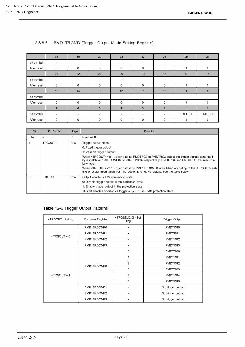
12.3.8.6 PMD1TRGMD (Trigger Output Mode Setting Register)
31 30 29 28 27 26 25 24
bit symbol - - - - - - - -
After reset 0 0 0 0 0 0 0 0
23 22 21 20 19 18 17 16
bit symbol - - - - - - - -
After reset 0 0 0 0 0 0 0 0
15 14 13 12 11 10 9 8
bit symbol - - - - - - - -
After reset 0 0 0 0 0 0 0 0
7 6 5 4 3 2 1 0
bit symbol - - - - - - TRGOUT EMGTGE
After reset 0 0 0 0 0 0 0 0
Bit Bit Symbol Type Function
31-2 - R Read as 0.
1 TRGOUT R/W Trigger output mode0: Fixed trigger output1: Variable trigger outputWhen <TRGOUT>="0", trigger outputs PMDTRG0 to PMDTRG3 output the trigger signals generatedby a match with <TRGCMP0> to <TRGCMP3> respectively. PMDTRG4 and PMDTRG5 are fixed to aLow level.When <TRGOUT>="1", trigger output by PMD1TRGCMP0 is switched according to the <TRGSEL> set-ting or sector information from the Vector Engine. For details, see the table below.
0 EMGTGE R/W Output enable in EMG protection state0: Disable trigger output in the protection state1: Enable trigger output in the protection stateThis bit enables or disables trigger output in the EMG protection state.
Table 12-6 Trigger Output Patterns
<TRGOUT> Setting Compare Register <TRGSEL[2:0]> Set-ting Trigger Output
<TRGOUT>=0
PMD1TRGCMP0 × PMDTRG0
PMD1TRGCMP1 × PMDTRG1
PMD1TRGCMP2 × PMDTRG2
PMD1TRGCMP3 × PMDTRG3
<TRGOUT>=1
PMD1TRGCMP0
0 PMDTRG0
1 PMDTRG1
2 PMDTRG2
3 PMDTRG3
4 PMDTRG4
5 PMDTRG5
PMD1TRGCMP1 × No trigger output
PMD1TRGCMP2 × No trigger output
PMD1TRGCMP3 × No trigger output
TMPM374FWUG
12. Motor Control Circuit (PMD: Programmable Motor Driver)
12.3 PMD Registers
Page 3842014/12/19

12.3.8.7 PMD1TRGSEL (Trigger Output Select Register)
31 30 29 28 27 26 25 24
bit symbol - - - - - - - -
After reset 0 0 0 0 0 0 0 0
23 22 21 20 19 18 17 16
bit symbol - - - - - - - -
After reset 0 0 0 0 0 0 0 0
15 14 13 12 11 10 9 8
bit symbol - - - - - - - -
After reset 0 0 0 0 0 0 0 0
7 6 5 4 3 2 1 0
bit symbol - - - - - TRGSEL
After reset 0 0 0 0 0 0 0 0
Bit Bit Symbol Type Function
31-2 - R Read as 0.
2-0 TRGSEL[2:0] R/W Trigger output select000: Output from PMDTRG0001: Output from PMDTRG1010: Output from PMDTRG2011: Output from PMDTRG3100: Output from PMDTRG4101: Output from PMDTRG5110: No trigger output111: No trigger outputThis field is effective when the variable trigger output mode is selected(PMD1TRGMD<TRGOUT>="1"). The selected trigger is output by a match between the PMD counterand the PMD1TRGCMP0 value. (See Table 12-6.)
TMPM374FWUG
Page 385 2014/12/19

TMPM374FWUG
12. Motor Control Circuit (PMD: Programmable Motor Driver)
12.3 PMD Registers
Page 3862014/12/19

13. Vector Engine (VE)
13.1 Overview
13.1.1 Features
The Vector Engine provides the following features:
1. Executes basic tasks for vector control (coordinate conversion, phase conversion and SIN/COScom-putation).
Uses fixed-point format data.
→No need for software to manage the decimal point alignment.
2. Enables interface (output control, trigger generation, input processing) with the motor control cir-cuit (PMD: Programmable Motor Driver) and AD converter (ADC).・ Converts computation results from fixed-point format to data format usable in the PMD.・ Generates timing data for interactive operation with the PMD and ADC.・ Converts AD conversion results into fixed-point format.
3. Calculates current, voltage and rotation speed by using normalized values with respect to their max-imum values in fixed-point format.
4. Implements PI control in current control.
5. Implements phase interpolation (integration of rotation speed).
PIcontrol
Current control
PIcontrol
IDREF
IQREF
Coordinateconversion
dq→AB
Phaseconversion
2→3
(SVM)
Vd
Vq
VA
VB
SIN/COS computasion
Phaseinterpolation
Coordinateconversion
dq←AB
SIN
COS
Phaseconversion
2←3
Inputprocessing
VDC
IuIvIw
IA
IB
VDC
Id
Iq
Id
Iq
Current/voltagedetection(ADC)
Outputcontrol
Triggergeneration
PWM outputsetting (PMD)
Sync. triggersetting (PMD)
DUTYaDUTYbDUTYcSECTOR
SIN,COSθ
ω
Figure 13-1 Block Diagram of Vector Control
TMPM374FWUG
Page 387 2014/12/19

13.1.2 Key Specifications
1. Space vector conversion is used for 2-phase-to-3-phase conversion. Both 2-phase modulation and 3-phase modulation are supported.
2. ADC sampling timing can be generated for sensorless current detection. Current detection can be per-formed by the 1-shunt, 3-shunt and 2-sensor methods.
3. In current control, PI control is implemented independently for d-axis and q-axis. It is also possibleto directly supply reference voltage information without using current control.
4. SIN/COS computations are performed with approximations using series values.Phase information can be directly specified or computed from rotation speed by using phase interpo-lation.
Note 1: For using the Vector Engine, the PMD must be set to the VE mode through the mode select register(PMD1MODESEL).
Note 2: It is also necessary to make appropriate settings in the ADC (enabling trigger and selecting AIN and re-sult registers to be used) for each synchronizing trigger from the PMD.
13.2 ConfigurationFigure 13-2 shows the configuration of the Vector Engine.
ADC Interupt
PWM Interrupt
VE Interrupt
Schedulemanagement
Schedule control
Start control
Error detection
Interrupt control
Tasks
Input voltage
Inputprocessing
Triggergeneration
Output control
Output voltage
Current ControlSchedule 0
Schedule 1
Schedule 9
Scheduler
ADC PMD
ComputationUnit
Registers
Decoder
Figure 13-2 Configuration of the Vector Engine
TMPM374FWUG
13. Vector Engine (VE)
13.2 Configuration
Page 3882014/12/19

13.2.1 Interaction among Vector Engine, Motor Control Circuit and A/D Converter
As shown in Figure 13-3, the Vector Engine allows direct interaction with the PMD and ADC.
When the PMD1MODESEL register is set to the VE mode, the PMD channel 1 registers PMD1CMPU,PMD1CMPV, PMD1CMPW, PMD1MDOUT, PMD1TRGCMP0, PMD1TRGCMP1 and PMD1TRGSEL areswitched to the Vector Engine registers VECMPU1, VECMPV1, VECMPW1, VEOUTCR1,VETRGCMP01, VETRGCMP11 and VETRGSEL1 respectively. In this case, these registers can only be con-trolled from the Vector Engine, and cannot be written from the PMD. Other PMD registers have no read/write restrictions.
The ADC unit B registers ADBREG0, ADBREG1, ADBREG2, ADBREG3 and ADABPSETn<UVWISn0[1:0]>, <UVWISn1[1:0]>, <UVWISn2[1:0]>, <UVWISn3[1:0]> which are read into the Vector Engine asthe Vector Engine registers VEADREG0B, VEADREG1B, VEADREG2B, VEADREG3B, VEPHNUM0B,VEPNNUM1B, VEPHNUM2B and VEPHNUM3B respectively. (These registers cannot be accessed fromthe CPU.) These ADC registers can be written and read from the ADC.
TMPM374FWUG
Page 389 2014/12/19

Channel 1 Output tasks
VETRGCMP01 register
VETRGCMP11 register
VEEMGRS1 register
VETRGSEL1 register
VEVCMPU1 register
VEVCMPV1 register
VEVCMPW1 register
VEOUTCR1 register
VEADREG0B
VEADREG1B
VEADREG2B
VEADREG3B
VEPHNUM0B
VEPHNUM1B
VEPHNUM2B
VEPHNUM3B
Channel 1 Input tasks
ADBREG1
ADBREG0
ADBREG2
ADBREG3
<UVWISn0>
<UVWISn1>
<UVWISn2>
<UVWISn3>
AD unit B
MUX
MUX
MUX
MUX
MUX
MUX
MUX
MUX
MUX
PMD Channel 1
Trigger generationBuffer
Buffer
Buffer
Buffer
Protectioncontrol
Buffer
Buffer
Buffer
Buffer
PWM generation Conductioncontrol
Port output
U1V1W1X1Y1Z1
PM
D1TR
G0 to 5
Trigger detection
Monitor function
AD conversion
Analog inputAINx
Vector Engine
PMD1CMPU
PMD1CMPV
PMD1CMPW
PMD1MDOUT
PMD1EMGCR <EMGRS>
PMD1TRGCMP0
PMD1TRGCMP1
PMDxTRGCMP2
PMD1TRGCMP3
PMD1TRGSEL
PMD1MODESEL
( n = 0 to 5 )
Figure 13-3 Interaction among Vector Engine, PMD and ADC
TMPM374FWUG
13. Vector Engine (VE)
13.2 Configuration
Page 3902014/12/19

13.3 List of RegistersThe Vector Engine registers are divided into the following three types:
・ VE control registers
Vector Engine control registers and temporary registers・ Common registers
Registers common to both channels・ Channel-specific registers
Computation data and control registers for each channel
13.3.1 List of Registers
VE Control Registers Base Address = 0x4005 _ 0000
Register Name Address
VE enable/disable VEEN R/W 0x0000
CPU start trigger selection VECPURUNTRG W 0x0004
Task selection VETASKAPP R/W 0x0008
Operation schedule selection VEACTSCH R/W 0x000C
Schedule repeat count VEREPTIME R/W 0x0010
Start trigger mode VETRGMODE R/W 0x0014
Error interrupt enable/disable VEERRINTEN R/W 0x0018
VE forced termination VECOMPEND W 0x001C
Error detection VEERRDET R 0x0020
Schedule executing flag/executing task VESCHTASKRUN R 0x0024
Reserved - R 0x0028
Temporary 0 VETMPREG0 R/W 0x002C
Temporary 1 VETMPREG1 R/W 0x0030
Temporary 2 VETMPREG2 R/W 0x0034
Temporary 3 VETMPREG3 R/W 0x0038
Temporary 4 VETMPREG4 R/W 0x003C
Temporary 5 VETMPREG5 R/W 0x0040
Reserved - R 0x01BC
Common Registers Base Address = 0x4005 _ 0000
Register Name Address
Reserved - R/W 0x0174
ADC conversion time (based on PWM clock) VETADC R/W 0x0178
TMPM374FWUG
Page 391 2014/12/19

Channel-Specific Registers for Channel 1 Base Address = 0x4005 _ 0000
Register Name Address
Status flags VEMCTLF1 R/W 0x00DC
Task control mode VEMODE1 R/W 0x00E0
Flow control VEFMODE1 R/W 0x00E4
PWM period rate (PWM period [s] × maximum speed (note1)×216) setting VETPWM1 R/W 0x00E8
Rotation speed (speed [Hz]÷ maximum speed(note1)×215)setting VEOMEGA1 R/W 0x00EC
Motor phase (motor phase [deg]/360×216) setting VETHETA1 R/W 0x00F0
d-axis reference value (current[A]÷maximum current (note2)×215) setting VEIDREF1 R/W 0x00F4
q-axis reference value (current[A]÷maximum current (note2)×215) setting VEIQREF1 R/W 0x00F8
d-axis voltage (voltage[V]÷maximum voltage (note3)×231) set-ting VEVD1 R/W 0x00FC
q-axis voltage (voltage[V]÷maximum voltage (note3)×231) set-ting VEVQ1 R/W 0x0100
Integral coefficient for PI control of d-axis VECIDKI1 R/W 0x0104
Proportional coefficient for PI control of d-axis VECIDKP1 R/W 0x0108
Integral coefficient for PI control of q-axis VECIQKI1 R/W 0x010C
Proportional coefficient for PI control of q-axis VECIQKP1 R/W 0x0110
Upper 32 bits of integral term (VDI ) of d-axis voltage VEVDIH1 R/W 0x0114
Lower 32 bits of integral term (VDI) of d-axis voltage VEVDILH1 R/W 0x0118
Upper 32 bits of integral term (VQI) of q-axis voltage VEVQIH1 R/W 0x011C
Lower 32 bits of integral term (VQI) of q-axis voltage VEVQILH1 R/W 0x0120
Switching speed (for 2-phase modulation and shift PWM) VEFPWMCHG1 R/W 0x0124
PWM period (to be set identically with PMD’s PWM period) VEMDPRD1 R/W 0x0128
Minimum pulse width VEMINPLS1 R/W 0x012C
Synchronizing trigger correction value VETRGCRC1 R/W 0x0130
Reserved - R/W 0x0134
Cosine value at THETA for output conversion (Q15 data) VECOS1 R/W 0x0138
Sine value at THETA for output conversion (Q15 data) VESIN1 R/W 0x014C
Previous cosine value for input processing (Q15 data) VECOSM1 R/W 0x0140
Previous sine value for input processing (Q15 data) VESINM1 R/W 0x0144
Sector information VESECTOR1 R/W 0x0148
Previous sector information for input processing VESECTORM1 R/W 0x014C
AD conversion result of a-phase zero-current (note4) VEIAO1 R/W 0x0150
AD conversion result of b-phase zero-current (note4) VEIBO1 R/W 0x0154
AD conversion result of c-phase zero-current (note4) VEICO1 R/W 0x0158
AD conversion result of a-phase current (note4) VEIAADC1 R/W 0x015C
AD conversion result of b-phase current (note4) VEIBADC1 R/W 0x0160
AD conversion result of c-phase current (note4) VEICADC1 R/W 0x0164
DC supply voltage (voltage[V]÷maximum voltage (note3)×215) VEVDC1 R/W 0x0168
d-axis current (current[A]÷maximum current (note2)×231) VEID1 R/W 0x016C
q-axis current (current[A]÷maximum current (note2)×231) VEIQ1 R/W 0x0170
PMD control: CMPU setting VECMPU1 R/W 0x019C
PMD control: CMPV setting VECMPV1 R/W 0x01A0
PMD control: CMPW setting VECMPW1 R/W 0x01A4
PMD control: Output control (MDOUT) VEOUTCR1 R/W 0x01A8
PMD control: TRGCMP0 setting VETRGCMP01 R/W 0x01AC
PMD control: TRGCMP1 setting VETRGCMP11 R/W 0x01B0
PMD control: Trigger selection VETRGSEL1 R/W 0x01B4
TMPM374FWUG
13. Vector Engine (VE)
13.3 List of Registers
Page 3922014/12/19

Channel-Specific Registers for Channel 1 Base Address = 0x4005 _ 0000
Register Name Address
PMD control: EMG return VEEMGRS1 W 0x01B8
Note 1: Maximum speed: Maximum rotation speed [Hz] that can be controlled or operated.Note 2: Maximum current:(Phase current value [A] which corresponds to 1 LSB of AD converter)× 211
Note 3: Maximum voltage: (Supply voltage (VDC) value [V] which corresponds to 1 LSB of AD conveter)× 212
Note 4: AD conversion results are stored in the upper 12 bits of each 16-bit register.
TMPM374FWUG
Page 393 2014/12/19

13.3.2 VE Control Registers
13.3.2.1 VEEN (VE enable/disable register)
31 30 29 28 27 26 25 24
bit symbol - - - - - - - -
After reset 0 0 0 0 0 0 0 0
23 22 21 20 19 18 17 16
bit symbol - - - - - - - -
After reset 0 0 0 0 0 0 0 0
15 14 13 12 11 10 9 8
bit symbol - - - - - - - -
After reset 0 0 0 0 0 0 0 0
7 6 5 4 3 2 1 0
bit symbol - - - - - - VEIDLEN VEEN
After reset 0 0 0 0 0 0 0 0
Bit Bit Symbol Type Function
31-2 − R Read as 0.
1 VEIDLEN R/W Controls whether or not the clock is supplied to the Vector Engine in IDLE mode.0: Inactive1: Active
0 VEEN R/W Disables or enables the Vector Engine.0: Disable1: Enable
TMPM374FWUG
13. Vector Engine (VE)
13.3 List of Registers
Page 3942014/12/19
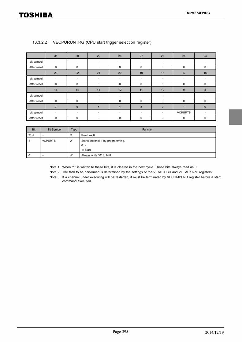
13.3.2.2 VECPURUNTRG (CPU start trigger selection register)
31 30 29 28 27 26 25 24
bit symbol - - - - - - - -
After reset 0 0 0 0 0 0 0 0
23 22 21 20 19 18 17 16
bit symbol - - - - - - - -
After reset 0 0 0 0 0 0 0 0
15 14 13 12 11 10 9 8
bit symbol - - - - - - - -
After reset 0 0 0 0 0 0 0 0
7 6 5 4 3 2 1 0
bit symbol - - - - - - VCPURTB -
After reset 0 0 0 0 0 0 0 0
Bit Bit Symbol Type Function
31-2 − R Read as 0.
1 VCPURTB W Starts channel 1 by programming.0: -1: Start
0 − W Always write "0" to bit0.
Note 1: When "1" is written to these bits, it is cleared in the next cycle. These bits always read as 0.Note 2: The task to be performed is determined by the settings of the VEACTSCH and VETASKAPP registers.Note 3: If a channel under executing will be restarted, it must be terminated by VECOMPEND register before a start
command executed.
TMPM374FWUG
Page 395 2014/12/19

13.3.2.3 VETASKAPP(Task selection register)
31 30 29 28 27 26 25 24
bit symbol - - - - - - - -
After reset 0 0 0 0 0 0 0 0
23 22 21 20 19 18 17 16
bit symbol - - - - - - - -
After reset 0 0 0 0 0 0 0 0
15 14 13 12 11 10 9 8
bit symbol - - - - - - - -
After reset 0 0 0 0 0 0 0 0
7 6 5 4 3 2 1 0
bit symbol VTASKB -
After reset 0 0 0 0 0 0 0 0
Bit Bit Symbol Type Function
31-8 − R Read as 0.
7-4 VTASKB[3:0] R/W Channel 1 task selection 0x0 : Output control0x1 : Trigger generation0x2 : Input processing0x3 : Input phase conversion0x4 : Input coordinate axis conversion0x5 : Current control0x6 : SIN/COS computation0x7 : Output coordinate axis conversion0x8 : Output phase conversion0x9 -0xF : Reserved Specifies the task to be performed when channel 1 is started by programming.
3-0 − R/W Always write "0000".
Note:Only those tasks that are included in schedules can be specified.
TMPM374FWUG
13. Vector Engine (VE)
13.3 List of Registers
Page 3962014/12/19

13.3.2.4 VEACTSCH (Operation schedule selection register)
31 30 29 28 27 26 25 24
bit symbol - - - - - - - -
After reset 0 0 0 0 0 0 0 0
23 22 21 20 19 18 17 16
bit symbol - - - - - - - -
After reset 0 0 0 0 0 0 0 0
15 14 13 12 11 10 9 8
bit symbol - - - - - - - -
After reset 0 0 0 0 0 0 0 0
7 6 5 4 3 2 1 0
bit symbol VACTB -
After reset 0 0 0 0 0 0 0 0
Bit Bit Symbol Type Function
31-8 − R Read as 0.
7-4 VACTB[3:0] R/W Specifies an individual task execution or a schedule for channel 1.0x0 : Individual task execution0x1 : Schedule 10x4 : Schedule 40x9 : Schedule 9Other : Reserved
3-0 − R/W Always write "0000".
TMPM374FWUG
Page 397 2014/12/19

13.3.2.5 VEREPTIME (Schedule repeat count)
31 30 29 28 27 26 25 24
bit symbol - - - - - - - -
After reset 0 0 0 0 0 0 0 0
23 22 21 20 19 18 17 16
bit symbol - - - - - - - -
After reset 0 0 0 0 0 0 0 0
15 14 13 12 11 10 9 8
bit symbol - - - - - - - -
After reset 0 0 0 0 0 0 0 0
7 6 5 4 3 2 1 0
bit symbol VREPB -
After reset 0 0 0 0 0 0 0 0
Bit Bit Symbol Type Function
31-8 − R Read as 0.
7-4 VREPB[3:0] R/W Specifies the repeat times a schedule is to be executed in channel 1.0: Do not execute schedule1 to 15: Execute schedule a specified number of times
3-0 − R/W Always write "00".
Note:When "0" is set, no schedule is executed.
TMPM374FWUG
13. Vector Engine (VE)
13.3 List of Registers
Page 3982014/12/19

13.3.2.6 VETRGMODE (Start trigger mode)
31 30 29 28 27 26 25 24
bit symbol - - - - - - - -
After reset 0 0 0 0 0 0 0 0
23 22 21 20 19 18 17 16
bit symbol - - - - - - - -
After reset 0 0 0 0 0 0 0 0
15 14 13 12 11 10 9 8
bit symbol - - - - - - - -
After reset 0 0 0 0 0 0 0 0
7 6 5 4 3 2 1 0
bit symbol - - - - VTRGB -
After reset 0 0 0 0 0 0 0 0
Bit Bit Symbol Type Function
31-4 − R Read as 0.
3-2 VTRGB[1:0] R/W Always write "10".
1-0 − R/W Always write "00".
TMPM374FWUG
Page 399 2014/12/19

13.3.2.7 VEERRINTEN (Error interrupt enable/disable)
31 30 29 28 27 26 25 24
bit symbol - - - - - - - -
After reset 0 0 0 0 0 0 0 0
23 22 21 20 19 18 17 16
bit symbol - - - - - - - -
After reset 0 0 0 0 0 0 0 0
15 14 13 12 11 10 9 8
bit symbol - - - - - - - -
After reset 0 0 0 0 0 0 0 0
7 6 5 4 3 2 1 0
bit symbol - - - - - - VERRENB -
After reset 0 0 0 0 0 0 0 0
Bit Bit Symbol Type Function
31-2 − R Read as 0.
1 VERRENB R/W Enables or disables the error detection interrupt in channel 1.0: Disable1: Enable
0 − R/W Always write "0".
TMPM374FWUG
13. Vector Engine (VE)
13.3 List of Registers
Page 4002014/12/19

13.3.2.8 VECOMPEND (VE forced termination)
31 30 29 28 27 26 25 24
bit symbol - - - - - - - -
After reset 0 0 0 0 0 0 0 0
23 22 21 20 19 18 17 16
bit symbol - - - - - - - -
After reset 0 0 0 0 0 0 0 0
15 14 13 12 11 10 9 8
bit symbol - - - - - - - -
After reset 0 0 0 0 0 0 0 0
7 6 5 4 3 2 1 0
bit symbol - - - - - - VCENDB -
After reset 0 0 0 0 0 0 0 0
Bit Bit Symbol Type Function
31-2 − R Read as 0.
1 VCENDB W Forcefully terminates the currently executing schedule in channel 1.0: −1: Terminate
0 − W Always write "0".
Note:When "1" is written to these bits, it is cleared in the next cycle. These bits always read as "0".
TMPM374FWUG
Page 401 2014/12/19
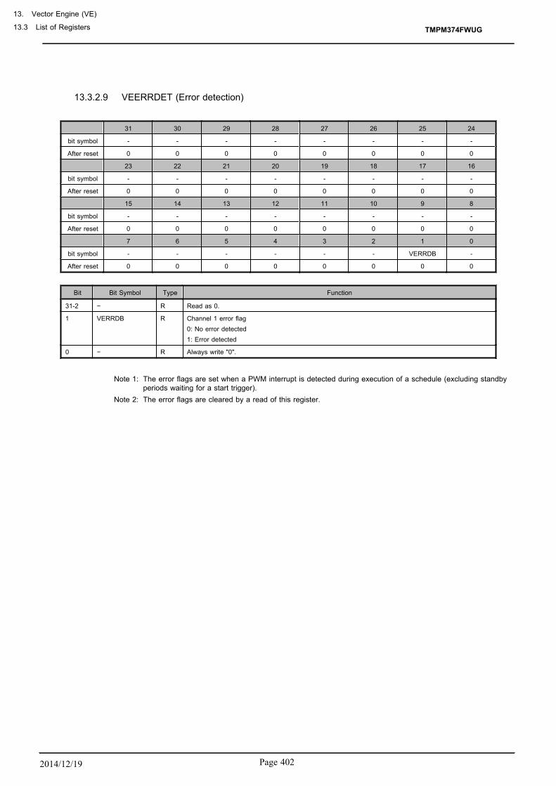
13.3.2.9 VEERRDET (Error detection)
31 30 29 28 27 26 25 24
bit symbol - - - - - - - -
After reset 0 0 0 0 0 0 0 0
23 22 21 20 19 18 17 16
bit symbol - - - - - - - -
After reset 0 0 0 0 0 0 0 0
15 14 13 12 11 10 9 8
bit symbol - - - - - - - -
After reset 0 0 0 0 0 0 0 0
7 6 5 4 3 2 1 0
bit symbol - - - - - - VERRDB -
After reset 0 0 0 0 0 0 0 0
Bit Bit Symbol Type Function
31-2 − R Read as 0.
1 VERRDB R Channel 1 error flag0: No error detected1: Error detected
0 − R Always write "0".
Note 1: The error flags are set when a PWM interrupt is detected during execution of a schedule (excluding standbyperiods waiting for a start trigger).
Note 2: The error flags are cleared by a read of this register.
TMPM374FWUG
13. Vector Engine (VE)
13.3 List of Registers
Page 4022014/12/19

13.3.2.10 VESCHTASKRUN (Schedule executing flag/executing task)
31 30 29 28 27 26 25 24
bit symbol - - - - - - - -
After reset 0 0 0 0 0 0 0 0
23 22 21 20 19 18 17 16
bit symbol - - - - - - - -
After reset 0 0 0 0 0 0 0 0
15 14 13 12 11 10 9 8
bit symbol - - - - - - VRTASKB
After reset 0 0 0 0 0 0 0 0
7 6 5 4 3 2 1 0
bit symbol VRTASKB VRSCHB - -
After reset 0 0 0 0 0 0 0 0
Bit Bit Symbol Type Function
31-10 − R Read as 0.
9-6 VRTASKB[3:0] R Task Number currently executing in channel 10x0: Output control0x1: Trigger generation0x2: Input processing0x3: Input phase conversion0x4: Input coordinate axis conversion0x5: Current control0x6: SIN/COS computation0x7: Output coordinate axis conversion0x8: Output phase conversion0x9 to 0xF: Reserved
5 VRSCHB R Schedule execution status in channel 10: Not executing1: Executing
4-0 − R Read as 0.
TMPM374FWUG
Page 403 2014/12/19

13.3.2.11 VETMPREG0 (Temporary register 0)
31 30 29 28 27 26 25 24
bit symbol TMPREG0
After reset 0 0 0 0 0 0 0 0
23 22 21 20 19 18 17 16
bit symbol TMPREG0
After reset 0 0 0 0 0 0 0 0
15 14 13 12 11 10 9 8
bit symbol TMPREG0
After reset 0 0 0 0 0 0 0 0
7 6 5 4 3 2 1 0
bit symbol TMPREG0
After reset 0 0 0 0 0 0 0 0
Bit Bit Symbol Type Function
31-0 TMPREG0[31:0] R/W Temporary register 0
13.3.2.12 VETMPREG1 (Temporary register 1)
31 30 29 28 27 26 25 24
bit symbol TMPREG1
After reset 0 0 0 0 0 0 0 0
23 22 21 20 19 18 17 16
bit symbol TMPREG1
After reset 0 0 0 0 0 0 0 0
15 14 13 12 11 10 9 8
bit symbol TMPREG1
After reset 0 0 0 0 0 0 0 0
7 6 5 4 3 2 1 0
bit symbol TMPREG1
After reset 0 0 0 0 0 0 0 0
Bit Bit Symbol Type Function
31-0 TMPREG1[31:0] R/W Temporary register 1
TMPM374FWUG
13. Vector Engine (VE)
13.3 List of Registers
Page 4042014/12/19
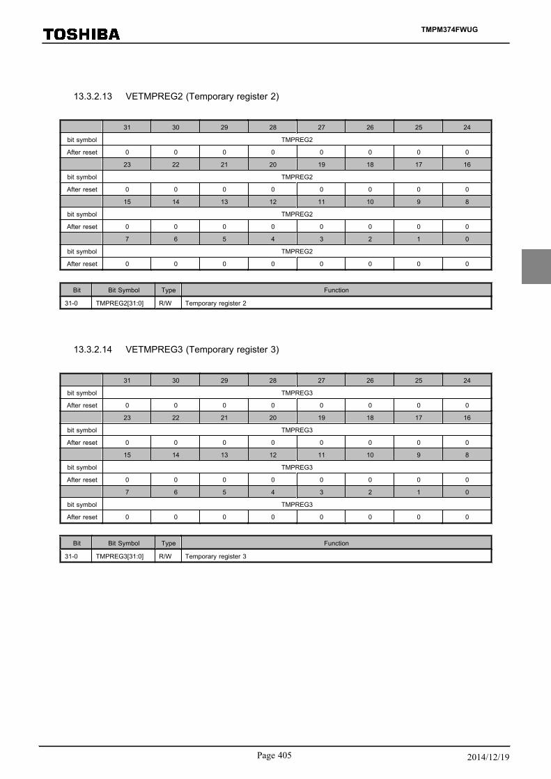
13.3.2.13 VETMPREG2 (Temporary register 2)
31 30 29 28 27 26 25 24
bit symbol TMPREG2
After reset 0 0 0 0 0 0 0 0
23 22 21 20 19 18 17 16
bit symbol TMPREG2
After reset 0 0 0 0 0 0 0 0
15 14 13 12 11 10 9 8
bit symbol TMPREG2
After reset 0 0 0 0 0 0 0 0
7 6 5 4 3 2 1 0
bit symbol TMPREG2
After reset 0 0 0 0 0 0 0 0
Bit Bit Symbol Type Function
31-0 TMPREG2[31:0] R/W Temporary register 2
13.3.2.14 VETMPREG3 (Temporary register 3)
31 30 29 28 27 26 25 24
bit symbol TMPREG3
After reset 0 0 0 0 0 0 0 0
23 22 21 20 19 18 17 16
bit symbol TMPREG3
After reset 0 0 0 0 0 0 0 0
15 14 13 12 11 10 9 8
bit symbol TMPREG3
After reset 0 0 0 0 0 0 0 0
7 6 5 4 3 2 1 0
bit symbol TMPREG3
After reset 0 0 0 0 0 0 0 0
Bit Bit Symbol Type Function
31-0 TMPREG3[31:0] R/W Temporary register 3
TMPM374FWUG
Page 405 2014/12/19

13.3.2.15 VETMPREG4 (Temporary register 4)
31 30 29 28 27 26 25 24
bit symbol TMPREG4
After reset 0 0 0 0 0 0 0 0
23 22 21 20 19 18 17 16
bit symbol TMPREG4
After reset 0 0 0 0 0 0 0 0
15 14 13 12 11 10 9 8
bit symbol TMPREG4
After reset 0 0 0 0 0 0 0 0
7 6 5 4 3 2 1 0
bit symbol TMPREG4
After reset 0 0 0 0 0 0 0 0
Bit Bit Symbol Type Function
31-0 TMPREG4[31:0] R/W Temporary register 4
13.3.2.16 VETMPREG5 (Temporary register 5)
31 30 29 28 27 26 25 24
bit symbol TMPREG5
After reset 0 0 0 0 0 0 0 0
23 22 21 20 19 18 17 16
bit symbol TMPREG5
After reset 0 0 0 0 0 0 0 0
15 14 13 12 11 10 9 8
bit symbol TMPREG5
After reset 0 0 0 0 0 0 0 0
7 6 5 4 3 2 1 0
bit symbol TMPREG5
After reset 0 0 0 0 0 0 0 0
Bit Bit Symbol Type Function
31-0 TMPREG5[31:0] R/W Temporary register 5
TMPM374FWUG
13. Vector Engine (VE)
13.3 List of Registers
Page 4062014/12/19
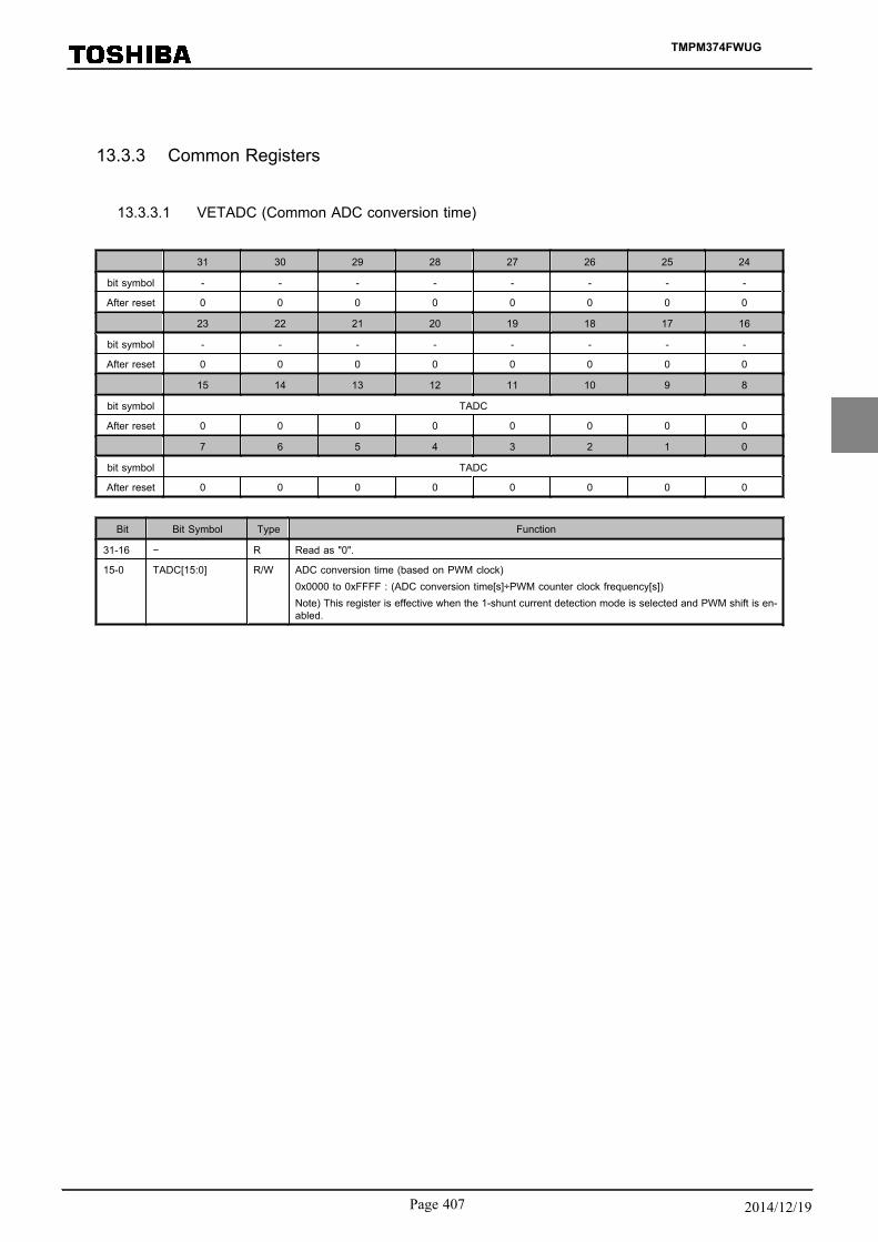
13.3.3 Common Registers
13.3.3.1 VETADC (Common ADC conversion time)
31 30 29 28 27 26 25 24
bit symbol - - - - - - - -
After reset 0 0 0 0 0 0 0 0
23 22 21 20 19 18 17 16
bit symbol - - - - - - - -
After reset 0 0 0 0 0 0 0 0
15 14 13 12 11 10 9 8
bit symbol TADC
After reset 0 0 0 0 0 0 0 0
7 6 5 4 3 2 1 0
bit symbol TADC
After reset 0 0 0 0 0 0 0 0
Bit Bit Symbol Type Function
31-16 − R Read as "0".
15-0 TADC[15:0] R/W ADC conversion time (based on PWM clock)0x0000 to 0xFFFF : (ADC conversion time[s]÷PWM counter clock frequency[s])Note) This register is effective when the 1-shunt current detection mode is selected and PWM shift is en-abled.
TMPM374FWUG
Page 407 2014/12/19

13.3.4 Channel-Specific Registers
13.3.4.1 VEMODE1 (Task control mode Registers)
31 30 29 28 27 26 25 24
bit symbol - - - - - - - -
After reset 0 0 0 0 0 0 0 0
23 22 21 20 19 18 17 16
bit symbol - - - - - - - -
After reset 0 0 0 0 0 0 0 0
15 14 13 12 11 10 9 8
bit symbol - - - - - - - -
After reset 0 0 0 0 0 0 0 0
7 6 5 4 3 2 1 0
bit symbol - - - - OCRMD ZIEN PVIEN
After reset 0 0 0 0 0 0 0 0
Bit Bit Symbol Type Function
31-8 − R Read as 0.
7-4 − R/W Always write "0".
3-2 OCRMD[1:0] R/W Output control00: Output OFF01: Output enable10: Reserved11: Output OFF and EMG return
1 ZIEN R/W Zero-current detection0: Disable1: Enable
0 PVIEN R/W Phase interpolation0: Disable1: Enable
TMPM374FWUG
13. Vector Engine (VE)
13.3 List of Registers
Page 4082014/12/19

13.3.4.2 VEFMODE1(Flow control Register)
31 30 29 28 27 26 25 24
bit symbol - - - - - - - -
After reset 0 0 0 0 0 0 0 0
23 22 21 20 19 18 17 16
bit symbol - - - - - - - -
After reset 0 0 0 0 0 0 0 0
15 14 13 12 11 10 9 8
bit symbol - - - - - - MREGDIS -
After reset 0 0 0 0 0 0 0 0
7 6 5 4 3 2 1 0
bit symbol - - - - IDMODE SPWMEN C2PEN
After reset 0 1 0 1 0 0 0 0
Bit Bit Symbol Type Function
31-16 − R Read as "0".
15-10 − R/W Always write "0".
9 MREGDIS R/W Keep the previous value of SIN/COS/SECTOR0: effective1: no_effectiveIn case of no_effective, VESINM1=VESIN1, VECOSM1=VECOS1, VESECTORM1=VESECTOR1.
8 − R/W Always write "0".
7-4 − R/W Always write "0101".
3-2 IDMODE R/W Current detection mode00: 3-shunt01: 2-sensor10: 1-shunt (for up count PMDTRG)11: 1-shunt (for down count PMDTRG)
1 SPWMEN R/W Enables or disables PWM shift.0: Disable1: Enable
0 C2PEN R/W Selects 3-phase or 2-phase modulation.0: 3-phase modulation1: 2-phase modulation
Note:When the 1-shunt mode is used, the acceptable PMDTRG is as follows.
VEFMODE1
<IDMODE[1:0]>PMD1TRGCR
<TRG0MD[2:0]>PMD1TRGCR
<TRG1MD[2:0]>
10 010(up-count) 010(up-count)
10 101(carrier bottom) 010(up-count)
11 001 (down-count) 001 (down-count)
11 001 (down-count) 101(carrier bottom)
TMPM374FWUG
Page 409 2014/12/19
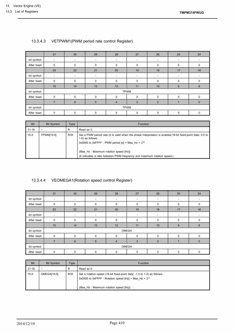
13.3.4.3 VETPWM1(PWM period rate control Register)
31 30 29 28 27 26 25 24
bit symbol - - - - - - - -
After reset 0 0 0 0 0 0 0 0
23 22 21 20 19 18 17 16
bit symbol - - - - - - - -
After reset 0 0 0 0 0 0 0 0
15 14 13 12 11 10 9 8
bit symbol TPWM
After reset 0 0 0 0 0 0 0 0
7 6 5 4 3 2 1 0
bit symbol TPWM
After reset 0 0 0 0 0 0 0 0
Bit Bit Symbol Type Function
31-16 − R Read as 0.
15-0 TPWM[15:0] R/W Set a PWM period rate (it is valid when the phase interpolation is enabled,16-bit fixed-point data: 0.0 to1.0) as follows:0x0000 to 0xFFFF : PWM period [s] × Max_Hz × 216
(Max_Hz : Maximum rotation speed [Hz])(It indicates a ratio between PWM frequency and maximum rotation speed.)
13.3.4.4 VEOMEGA1(Rotation speed control Register)
31 30 29 28 27 26 25 24
bit symbol - - - - - - - -
After reset 0 0 0 0 0 0 0 0
23 22 21 20 19 18 17 16
bit symbol - - - - - - - -
After reset 0 0 0 0 0 0 0 0
15 14 13 12 11 10 9 8
bit symbol OMEGA
After reset 0 0 0 0 0 0 0 0
7 6 5 4 3 2 1 0
bit symbol OMEGA
After reset 0 0 0 0 0 0 0 0
Bit Bit Symbol Type Function
31-16 − R Read as 0.
15-0 OMEGA[15:0] R/W Set a rotation speed (16-bit fixed-point data: -1.0 to 1.0) as follows:0x0000 to 0xFFFF : Rotation speed [Hz] ÷ Max_Hz × 215
(Max_Hz : Maximum rotation speed [Hz])
TMPM374FWUG
13. Vector Engine (VE)
13.3 List of Registers
Page 4102014/12/19

13.3.4.5 VETHETA1(Motor phase control Register)
31 30 29 28 27 26 25 24
bit symbol - - - - - - - -
After reset 0 0 0 0 0 0 0 0
23 22 21 20 19 18 17 16
bit symbol - - - - - - - -
After reset 0 0 0 0 0 0 0 0
15 14 13 12 11 10 9 8
bit symbol THETA
After reset 0 0 0 0 0 0 0 0
7 6 5 4 3 2 1 0
bit symbol THETA
After reset 0 0 0 0 0 0 0 0
Bit Bit Symbol Type Function
31-16 − R Read as 0.
15-0 THETA[15:0] R/W Set phase data (16-bit fixed-point data: 0.0 to 1.0) as follows:Formula : Phase[deg] ÷ 360 × 216
13.3.4.6 VECOS1/VESIN1/VECOSM1/VESINM1
VECOS1 (Cosine value at THETA for output conversion (Q15 data))
31 30 29 28 27 26 25 24
bit symbol - - - - - - - -
After reset 0 0 0 0 0 0 0 0
23 22 21 20 19 18 17 16
bit symbol - - - - - - - -
After reset 0 0 0 0 0 0 0 0
15 14 13 12 11 10 9 8
bit symbol COS
After reset 0 0 0 0 0 0 0 0
7 6 5 4 3 2 1 0
bit symbol COS
After reset 0 0 0 0 0 0 0 0
Bit Bit Symbol Type Function
31-16 − R Read as "0".
15-0 COS[15:0] R/W Cosine value based on the THETA value (16-bit fixed-point data: -1.0 to 1.0)Cosine value: 0x0000 to 0xFFFF
TMPM374FWUG
Page 411 2014/12/19

VESIN1 (Sine value at THETA for output conversion (Q15 data))
31 30 29 28 27 26 25 24
bit symbol - - - - - - - -
After reset 0 0 0 0 0 0 0 0
23 22 21 20 19 18 17 16
bit symbol - - - - - - - -
After reset 0 0 0 0 0 0 0 0
15 14 13 12 11 10 9 8
bit symbol SIN
After reset 0 0 0 0 0 0 0 0
7 6 5 4 3 2 1 0
bit symbol SIN
After reset 0 0 0 0 0 0 0 0
Bit Bit Symbol Type Function
31-16 − R Read as "0".
15-0 SIN[15:0] R/W Sine value based on the THETA value (16-bit fixed-point data: -1.0 to 1.0)Sine value: 0x0000 to 0xFFFF
VECOSM1
31 30 29 28 27 26 25 24
bit symbol - - - - - - - -
After reset 0 0 0 0 0 0 0 0
23 22 21 20 19 18 17 16
bit symbol - - - - - - - -
After reset 0 0 0 0 0 0 0 0
15 14 13 12 11 10 9 8
bit symbol COSM
After reset 0 0 0 0 0 0 0 0
7 6 5 4 3 2 1 0
bit symbol COSM
After reset 0 0 0 0 0 0 0 0
Bit Bit Symbol Type Function
31-16 − R Read as "0".
15-0 COSM[15:0] R/W Previous value of the COS registerCosine value (previous value): 0x0000 to 0xFFFF
TMPM374FWUG
13. Vector Engine (VE)
13.3 List of Registers
Page 4122014/12/19
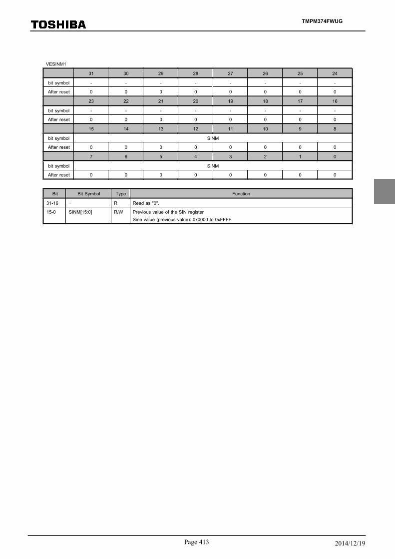
VESINM1
31 30 29 28 27 26 25 24
bit symbol - - - - - - - -
After reset 0 0 0 0 0 0 0 0
23 22 21 20 19 18 17 16
bit symbol - - - - - - - -
After reset 0 0 0 0 0 0 0 0
15 14 13 12 11 10 9 8
bit symbol SINM
After reset 0 0 0 0 0 0 0 0
7 6 5 4 3 2 1 0
bit symbol SINM
After reset 0 0 0 0 0 0 0 0
Bit Bit Symbol Type Function
31-16 − R Read as "0".
15-0 SINM[15:0] R/W Previous value of the SIN registerSine value (previous value): 0x0000 to 0xFFFF
TMPM374FWUG
Page 413 2014/12/19

13.3.4.7 VEIDREF1/VEIQREF1(dq Current Reference Registers)
VEIDREF1
31 30 29 28 27 26 25 24
bit symbol - - - - - - - -
After reset 0 0 0 0 0 0 0 0
23 22 21 20 19 18 17 16
bit symbol - - - - - - - -
After reset 0 0 0 0 0 0 0 0
15 14 13 12 11 10 9 8
bit symbol IDREF
After reset 0 0 0 0 0 0 0 0
7 6 5 4 3 2 1 0
bit symbol IDREF
After reset 0 0 0 0 0 0 0 0
Bit Bit Symbol Type Function
31-16 − R Read as "0".
15-0 IDREF[15:0] R/W Reference value of d-axis current (16-bit fixed-point data: -1.0 to 1.0)0x0000 to 0xFFFF(The value to be set is : d-axis current reference[A]÷Max_I×215) Max_I: (Phase current value [A] which corresponds to 1 LSB of ADC)×211
VEIQREF1
31 30 29 28 27 26 25 24
bit symbol - - - - - - - -
After reset 0 0 0 0 0 0 0 0
23 22 21 20 19 18 17 16
bit symbol - - - - - - - -
After reset 0 0 0 0 0 0 0 0
15 14 13 12 11 10 9 8
bit symbol IQREF
After reset 0 0 0 0 0 0 0 0
7 6 5 4 3 2 1 0
bit symbol IQREF
After reset 0 0 0 0 0 0 0 0
Bit Bit Symbol Type Function
31-16 − R Read as "0".
15-0 IQREF[15:0] R/W Reference value of q-axis current (16-bit fixed-point data: -1.0 to 1.0)0x0000 to 0xFFFF(The value to be set is : q-axis current reference [A]÷Max_I×215) Max_I: (Phase current value [A] which corresponds to 1 LSB of ADC)×211
TMPM374FWUG
13. Vector Engine (VE)
13.3 List of Registers
Page 4142014/12/19
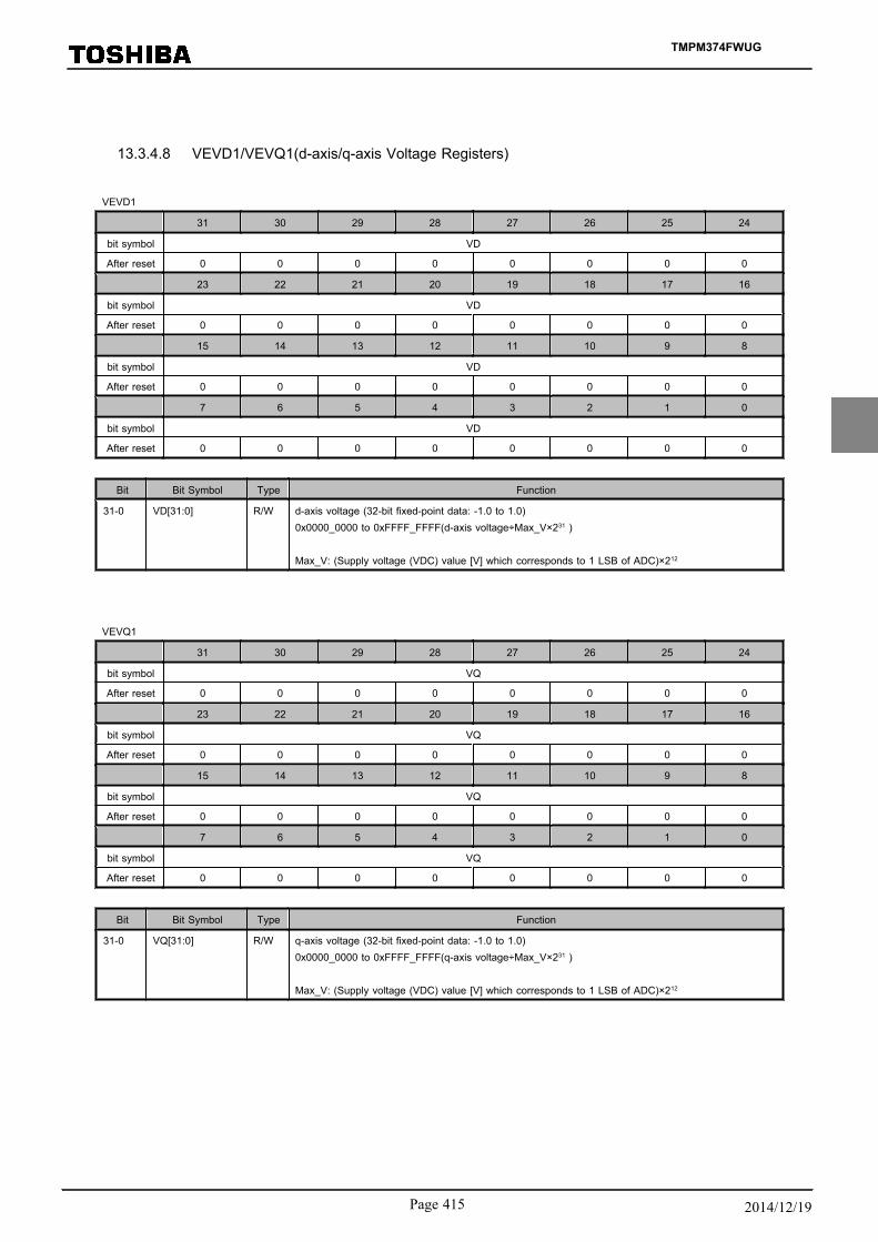
13.3.4.8 VEVD1/VEVQ1(d-axis/q-axis Voltage Registers)
VEVD1
31 30 29 28 27 26 25 24
bit symbol VD
After reset 0 0 0 0 0 0 0 0
23 22 21 20 19 18 17 16
bit symbol VD
After reset 0 0 0 0 0 0 0 0
15 14 13 12 11 10 9 8
bit symbol VD
After reset 0 0 0 0 0 0 0 0
7 6 5 4 3 2 1 0
bit symbol VD
After reset 0 0 0 0 0 0 0 0
Bit Bit Symbol Type Function
31-0 VD[31:0] R/W d-axis voltage (32-bit fixed-point data: -1.0 to 1.0)0x0000_0000 to 0xFFFF_FFFF(d-axis voltage÷Max_V×231 ) Max_V: (Supply voltage (VDC) value [V] which corresponds to 1 LSB of ADC)×212
VEVQ1
31 30 29 28 27 26 25 24
bit symbol VQ
After reset 0 0 0 0 0 0 0 0
23 22 21 20 19 18 17 16
bit symbol VQ
After reset 0 0 0 0 0 0 0 0
15 14 13 12 11 10 9 8
bit symbol VQ
After reset 0 0 0 0 0 0 0 0
7 6 5 4 3 2 1 0
bit symbol VQ
After reset 0 0 0 0 0 0 0 0
Bit Bit Symbol Type Function
31-0 VQ[31:0] R/W q-axis voltage (32-bit fixed-point data: -1.0 to 1.0)0x0000_0000 to 0xFFFF_FFFF(q-axis voltage÷Max_V×231 ) Max_V: (Supply voltage (VDC) value [V] which corresponds to 1 LSB of ADC)×212
TMPM374FWUG
Page 415 2014/12/19

13.3.4.9 VECIDKI1/VECIDKP1/VEVCIQKI1/VECIQKP1(PI Control Coefficient Registers)
VECIDKI1
31 30 29 28 27 26 25 24
bit symbol - - - - - - - -
After reset 0 0 0 0 0 0 0 0
23 22 21 20 19 18 17 16
bit symbol - - - - - - - -
After reset 0 0 0 0 0 0 0 0
15 14 13 12 11 10 9 8
bit symbol CIDKI
After reset 0 0 0 0 0 0 0 0
7 6 5 4 3 2 1 0
bit symbol CIDKI
After reset 0 0 0 0 0 0 0 0
Bit Bit Symbol Type Function
31-16 − R Read as "0".
15-0 CIDKI[15:0] R/W Integral coefficient for PI control of d-axis: 0x0000 to 0xFFFF
VECIDKP1
31 30 29 28 27 26 25 24
bit symbol - - - - - - - -
After reset 0 0 0 0 0 0 0 0
23 22 21 20 19 18 17 16
bit symbol - - - - - - - -
After reset 0 0 0 0 0 0 0 0
15 14 13 12 11 10 9 8
bit symbol CIDKP
After reset 0 0 0 0 0 0 0 0
7 6 5 4 3 2 1 0
bit symbol CIDKP
After reset 0 0 0 0 0 0 0 0
Bit Bit Symbol Type Function
31-16 − R Read as "0".
15-0 CIDKP[15:0] R/W Proportional coefficient for PI control of d-axis: 0x0000 to 0xFFFF
TMPM374FWUG
13. Vector Engine (VE)
13.3 List of Registers
Page 4162014/12/19
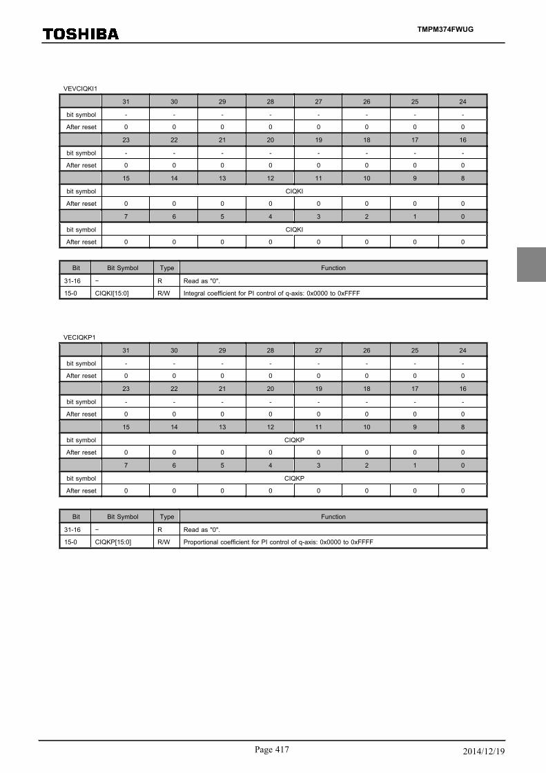
VEVCIQKI1
31 30 29 28 27 26 25 24
bit symbol - - - - - - - -
After reset 0 0 0 0 0 0 0 0
23 22 21 20 19 18 17 16
bit symbol - - - - - - - -
After reset 0 0 0 0 0 0 0 0
15 14 13 12 11 10 9 8
bit symbol CIQKI
After reset 0 0 0 0 0 0 0 0
7 6 5 4 3 2 1 0
bit symbol CIQKI
After reset 0 0 0 0 0 0 0 0
Bit Bit Symbol Type Function
31-16 − R Read as "0".
15-0 CIQKI[15:0] R/W Integral coefficient for PI control of q-axis: 0x0000 to 0xFFFF
VECIQKP1
31 30 29 28 27 26 25 24
bit symbol - - - - - - - -
After reset 0 0 0 0 0 0 0 0
23 22 21 20 19 18 17 16
bit symbol - - - - - - - -
After reset 0 0 0 0 0 0 0 0
15 14 13 12 11 10 9 8
bit symbol CIQKP
After reset 0 0 0 0 0 0 0 0
7 6 5 4 3 2 1 0
bit symbol CIQKP
After reset 0 0 0 0 0 0 0 0
Bit Bit Symbol Type Function
31-16 − R Read as "0".
15-0 CIQKP[15:0] R/W Proportional coefficient for PI control of q-axis: 0x0000 to 0xFFFF
TMPM374FWUG
Page 417 2014/12/19

13.3.4.10 VEVDIH1/VEVDILH1/VEVQIH1/VEVQILH1(PI Control Integral Term Registers)
VEVDIH1
31 30 29 28 27 26 25 24
bit symbol VDIH
After reset 0 0 0 0 0 0 0 0
23 22 21 20 19 18 17 16
bit symbol VDIH
After reset 0 0 0 0 0 0 0 0
15 14 13 12 11 10 9 8
bit symbol VDIH
After reset 0 0 0 0 0 0 0 0
7 6 5 4 3 2 1 0
bit symbol VDIHI
After reset 0 0 0 0 0 0 0 0
Bit Bit Symbol Type Function
31-0 VDIH[31:0] R/W Upper 32 bits of the integral term (VDI) for PI control of d-axis
VEVDILH1
31 30 29 28 27 26 25 24
bit symbol VDILH
After reset 0 0 0 0 0 0 0 0
23 22 21 20 19 18 17 16
bit symbol VDILH
After reset 0 0 0 0 0 0 0 0
15 14 13 12 11 10 9 8
bit symbol - - - - - - - -
After reset 0 0 0 0 0 0 0 0
7 6 5 4 3 2 1 0
bit symbol - - - - - - - -
After reset 0 0 0 0 0 0 0 0
Bit Bit Symbol Type Function
31-16 VDILH[15:0] R/W Bit 31 to 16 of the integral term (VDI) for PI control of d-axis
15-0 − R Read as 0.
Note:64-bit fixed-point data with 63 fractional bits (-1.0 to 1.0)
TMPM374FWUG
13. Vector Engine (VE)
13.3 List of Registers
Page 4182014/12/19

VEVQIH1
31 30 29 28 27 26 25 24
bit symbol VQIH
After reset 0 0 0 0 0 0 0 0
23 22 21 20 19 18 17 16
bit symbol VQIH
After reset 0 0 0 0 0 0 0 0
15 14 13 12 11 10 9 8
bit symbol VQIH
After reset 0 0 0 0 0 0 0 0
7 6 5 4 3 2 1 0
bit symbol VQIH
After reset 0 0 0 0 0 0 0 0
Bit Bit Symbol Type Function
31-0 VQIH[31:0] R/W Upper 32 bits of the integral term (VQI) for PI control of q-axis
VEVQILH1
31 30 29 28 27 26 25 24
bit symbol VQILH
After reset 0 0 0 0 0 0 0 0
23 22 21 20 19 18 17 16
bit symbol VQILH
After reset 0 0 0 0 0 0 0 0
15 14 13 12 11 10 9 8
bit symbol - - - - - - - -
After reset 0 0 0 0 0 0 0 0
7 6 5 4 3 2 1 0
bit symbol - - - - - - - -
After reset 0 0 0 0 0 0 0 0
Bit Bit Symbol Type Function
31-16 VQILH[15:0] R/W Bit 31 to 16 of the integral term (VQI) for PI control of q-axis
15-0 − R Read as 0.
Note:64-bit fixed-point data with 63 fractional bits (-1.0 to 1.0)
TMPM374FWUG
Page 419 2014/12/19

13.3.4.11 VEMCTLF1(Status flags Register)
31 30 29 28 27 26 25 24
bit symbol - - - - - - - -
After reset 0 0 0 0 0 0 0 0
23 22 21 20 19 18 17 16
bit symbol - - - - - - - -
After reset 0 0 0 0 0 0 0 0
15 14 13 12 11 10 9 8
bit symbol - - - - - - - -
After reset 0 0 0 0 0 0 0 0
7 6 5 4 3 2 1 0
bit symbol - - PLSLFM PLSLF - LVTF LAVFM LAVF
After reset 0 0 0 0 0 0 0 0
Bit Bit Symbol Type Function
31-8 − R Read as 0.
7-6 − R/W Always write "0".
5 PLSLFM R/W Previous value of <PLSLF>
4 PLSLF R/W Minimum disparity of pulse width
Minimum disparityof pulse width
< VEMINPLS1<MINPLS> case ="1"
3 − R/W Always write "0".
2 LVTF R/W Supply voltage lower flag
VEVDC1<VDC> ≥ 0x0100 (1/128) case="0"
VEVDC1<VDC> < 0x0100 (1/128) case="1"
1 LAVFM R/W Previous <LAVF> value
0 LAVF R/W Low-speed flag0: High-speed1: Low-speed
VEOMEGA1<OMEGA> ≥ VEFPWMCHG1<FPWMCHG> case="0"
VEOMEGA1<OMEGA> < VEFPWMCHG1<FPWMCHG> case="1"
TMPM374FWUG
13. Vector Engine (VE)
13.3 List of Registers
Page 4202014/12/19
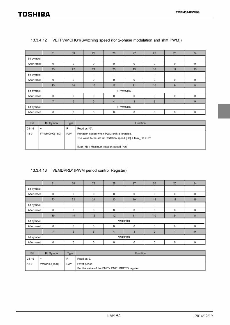
13.3.4.12 VEFPWMCHG1(Switching speed (for 2-phase modulation and shift PWM))
31 30 29 28 27 26 25 24
bit symbol - - - - - - - -
After reset 0 0 0 0 0 0 0 0
23 22 21 20 19 18 17 16
bit symbol - - - - - - - -
After reset 0 0 0 0 0 0 0 0
15 14 13 12 11 10 9 8
bit symbol FPWMCHG
After reset 0 0 0 0 0 0 0 0
7 6 5 4 3 2 1 0
bit symbol FPWMCHG
After reset 0 0 0 0 0 0 0 0
Bit Bit Symbol Type Function
31-16 − R Read as "0".
15-0 FPWMCHG[15:0] R/W Rortation speed when PWM shift is enabled.The value to be set is: Rortation speed [Hz] ÷ Max_Hz × 215
(Max_Hz : Maximum rotation speed [Hz])
13.3.4.13 VEMDPRD1(PWM period control Register)
31 30 29 28 27 26 25 24
bit symbol - - - - - - - -
After reset 0 0 0 0 0 0 0 0
23 22 21 20 19 18 17 16
bit symbol - - - - - - - -
After reset 0 0 0 0 0 0 0 0
15 14 13 12 11 10 9 8
bit symbol VMDPRD
After reset 0 0 0 0 0 0 0 0
7 6 5 4 3 2 1 0
bit symbol VMDPRD
After reset 0 0 0 0 0 0 0 0
Bit Bit Symbol Type Function
31-16 − R Read as 0.
15-0 VMDPRD[15:0] R/W PWM periodSet the value of the PMD’s PMD1MDPRD register.
TMPM374FWUG
Page 421 2014/12/19
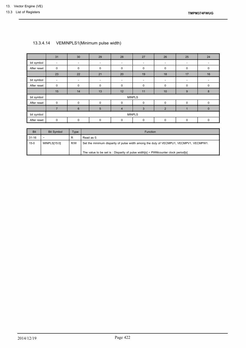
13.3.4.14 VEMINPLS1(Minimum pulse width)
31 30 29 28 27 26 25 24
bit symbol - - - - - - - -
After reset 0 0 0 0 0 0 0 0
23 22 21 20 19 18 17 16
bit symbol - - - - - - - -
After reset 0 0 0 0 0 0 0 0
15 14 13 12 11 10 9 8
bit symbol MINPLS
After reset 0 0 0 0 0 0 0 0
7 6 5 4 3 2 1 0
bit symbol MINPLS
After reset 0 0 0 0 0 0 0 0
Bit Bit Symbol Type Function
31-16 − R Read as 0.
15-0 MINPLS[15:0] R/W Set the minimum disparity of pulse width among the duty of VECMPU1, VECMPV1, VECMPW1. The value to be set is : Disparity of pulse width[s] ÷ PWMcounter clock period[s]
TMPM374FWUG
13. Vector Engine (VE)
13.3 List of Registers
Page 4222014/12/19
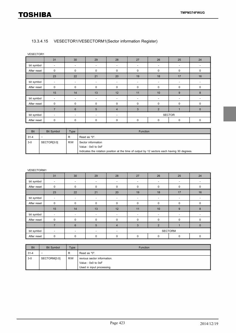
13.3.4.15 VESECTOR1/VESECTORM1(Sector information Register)
VESECTOR1
31 30 29 28 27 26 25 24
bit symbol - - - - - - - -
After reset 0 0 0 0 0 0 0 0
23 22 21 20 19 18 17 16
bit symbol - - - - - - - -
After reset 0 0 0 0 0 0 0 0
15 14 13 12 11 10 9 8
bit symbol - - - - - - - -
After reset 0 0 0 0 0 0 0 0
7 6 5 4 3 2 1 0
bit symbol - - - - SECTOR
After reset 0 0 0 0 0 0 0 0
Bit Bit Symbol Type Function
31-4 − R Read as "0".
3-0 SECTOR[3:0] R/W Sector informationValue : 0x0 to 0xFIndicates the rotation position at the time of output by 12 sectors each having 30 degrees.
VESECTORM1
31 30 29 28 27 26 25 24
bit symbol - - - - - - - -
After reset 0 0 0 0 0 0 0 0
23 22 21 20 19 18 17 16
bit symbol - - - - - - - -
After reset 0 0 0 0 0 0 0 0
15 14 13 12 11 10 9 8
bit symbol - - - - - - - -
After reset 0 0 0 0 0 0 0 0
7 6 5 4 3 2 1 0
bit symbol - - - - SECTORM
After reset 0 0 0 0 0 0 0 0
Bit Bit Symbol Type Function
31-4 − R Read as "0".
3-0 SECTORM[3:0] R/W revious sector information.Value : 0x0 to 0xFUsed in input processing.
TMPM374FWUG
Page 423 2014/12/19
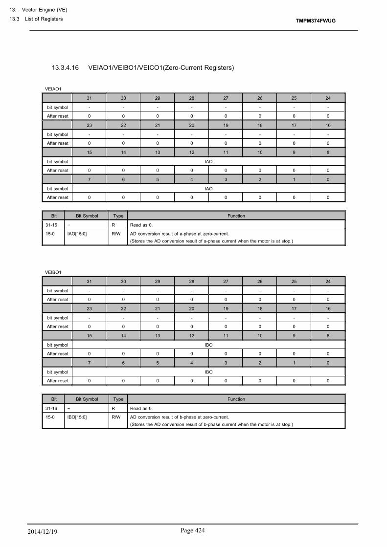
13.3.4.16 VEIAO1/VEIBO1/VEICO1(Zero-Current Registers)
VEIAO1
31 30 29 28 27 26 25 24
bit symbol - - - - - - - -
After reset 0 0 0 0 0 0 0 0
23 22 21 20 19 18 17 16
bit symbol - - - - - - - -
After reset 0 0 0 0 0 0 0 0
15 14 13 12 11 10 9 8
bit symbol IAO
After reset 0 0 0 0 0 0 0 0
7 6 5 4 3 2 1 0
bit symbol IAO
After reset 0 0 0 0 0 0 0 0
Bit Bit Symbol Type Function
31-16 − R Read as 0.
15-0 IAO[15:0] R/W AD conversion result of a-phase at zero-current.(Stores the AD conversion result of a-phase current when the motor is at stop.)
VEIBO1
31 30 29 28 27 26 25 24
bit symbol - - - - - - - -
After reset 0 0 0 0 0 0 0 0
23 22 21 20 19 18 17 16
bit symbol - - - - - - - -
After reset 0 0 0 0 0 0 0 0
15 14 13 12 11 10 9 8
bit symbol IBO
After reset 0 0 0 0 0 0 0 0
7 6 5 4 3 2 1 0
bit symbol IBO
After reset 0 0 0 0 0 0 0 0
Bit Bit Symbol Type Function
31-16 − R Read as 0.
15-0 IBO[15:0] R/W AD conversion result of b-phase at zero-current.(Stores the AD conversion result of b-phase current when the motor is at stop.)
TMPM374FWUG
13. Vector Engine (VE)
13.3 List of Registers
Page 4242014/12/19

VEICO1
31 30 29 28 27 26 25 24
bit symbol - - - - - - - -
After reset 0 0 0 0 0 0 0 0
23 22 21 20 19 18 17 16
bit symbol - - - - - - - -
After reset 0 0 0 0 0 0 0 0
15 14 13 12 11 10 9 8
bit symbol ICO
After reset 0 0 0 0 0 0 0 0
7 6 5 4 3 2 1 0
bit symbol ICO
After reset 0 0 0 0 0 0 0 0
Bit Bit Symbol Type Function
31-16 − R Read as "0".
15-0 ICO[15:0] R/W AD conversion result of c-phase at zero-current.(Stores the AD conversion result of c-phase current when the motor is at stop.)
Note 1: When the zero-current detection is enabled, AD conversion results are automatically stored to these registers.Note 2: AD conversion results are stored in the 15 to 4 bits, with the 3 to 0 bits always "0".
TMPM374FWUG
Page 425 2014/12/19

13.3.4.17 VEIAADC1/VEIBADC1/VEICADC1(Current ADC Result Registers)
VEIAADC1
31 30 29 28 27 26 25 24
bit symbol - - - - - - - -
After reset 0 0 0 0 0 0 0 0
23 22 21 20 19 18 17 16
bit symbol - - - - - - - -
After reset 0 0 0 0 0 0 0 0
15 14 13 12 11 10 9 8
bit symbol IAADC
After reset 0 0 0 0 0 0 0 0
7 6 5 4 3 2 1 0
bit symbol IAADC
After reset 0 0 0 0 0 0 0 0
Bit Bit Symbol Type Function
31-16 − R Read as 0.
15-0 IAADC[15:0] R/W Stores the AD conversion result of a-phase current: 0x0000 to 0xFFFF
VEIBADC1
31 30 29 28 27 26 25 24
bit symbol - - - - - - - -
After reset 0 0 0 0 0 0 0 0
23 22 21 20 19 18 17 16
bit symbol - - - - - - - -
After reset 0 0 0 0 0 0 0 0
15 14 13 12 11 10 9 8
bit symbol IBADC
After reset 0 0 0 0 0 0 0 0
7 6 5 4 3 2 1 0
bit symbol IBADC
After reset 0 0 0 0 0 0 0 0
Bit Bit Symbol Type Function
31-16 − R Read as "0".
15-0 IBADC[15:0] R/W Stores the AD conversion result of b-phase current: 0x0000 to 0xFFFF
TMPM374FWUG
13. Vector Engine (VE)
13.3 List of Registers
Page 4262014/12/19
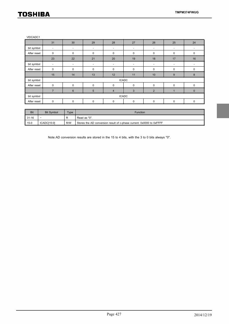
VEICADC1
31 30 29 28 27 26 25 24
bit symbol - - - - - - - -
After reset 0 0 0 0 0 0 0 0
23 22 21 20 19 18 17 16
bit symbol - - - - - - - -
After reset 0 0 0 0 0 0 0 0
15 14 13 12 11 10 9 8
bit symbol ICADC
After reset 0 0 0 0 0 0 0 0
7 6 5 4 3 2 1 0
bit symbol ICADC
After reset 0 0 0 0 0 0 0 0
Bit Bit Symbol Type Function
31-16 − R Read as "0".
15-0 ICADC[15:0] R/W Stores the AD conversion result of c-phase current: 0x0000 to 0xFFFF
Note:AD conversion results are stored in the 15 to 4 bits, with the 3 to 0 bits always "0".
TMPM374FWUG
Page 427 2014/12/19
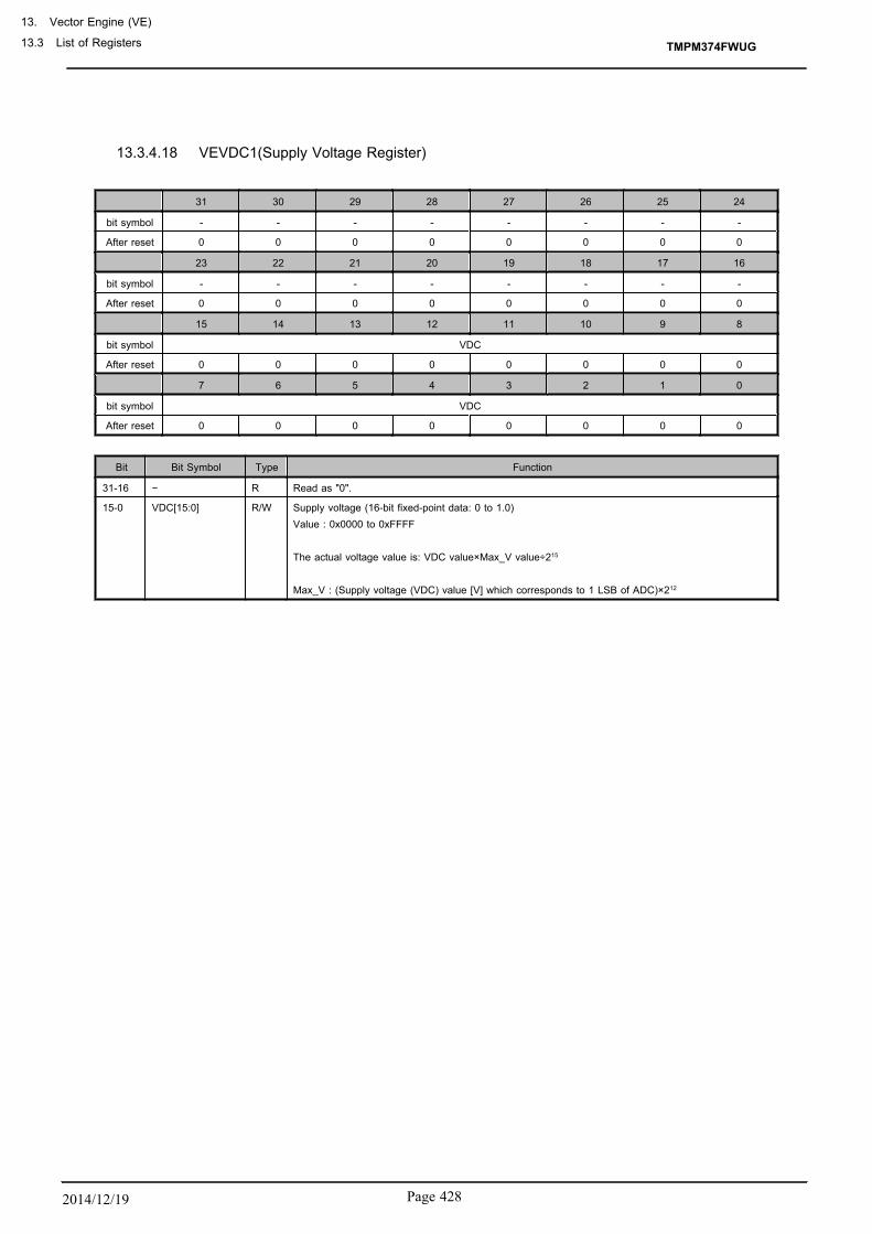
13.3.4.18 VEVDC1(Supply Voltage Register)
31 30 29 28 27 26 25 24
bit symbol - - - - - - - -
After reset 0 0 0 0 0 0 0 0
23 22 21 20 19 18 17 16
bit symbol - - - - - - - -
After reset 0 0 0 0 0 0 0 0
15 14 13 12 11 10 9 8
bit symbol VDC
After reset 0 0 0 0 0 0 0 0
7 6 5 4 3 2 1 0
bit symbol VDC
After reset 0 0 0 0 0 0 0 0
Bit Bit Symbol Type Function
31-16 − R Read as "0".
15-0 VDC[15:0] R/W Supply voltage (16-bit fixed-point data: 0 to 1.0)Value : 0x0000 to 0xFFFF The actual voltage value is: VDC value×Max_V value÷215
Max_V : (Supply voltage (VDC) value [V] which corresponds to 1 LSB of ADC)×212
TMPM374FWUG
13. Vector Engine (VE)
13.3 List of Registers
Page 4282014/12/19

13.3.4.19 VEID1/VEIQ1(d-axis/q-axis Current Registers)
VEID1
31 30 29 28 27 26 25 24
bit symbol ID
After reset 0 0 0 0 0 0 0 0
23 22 21 20 19 18 17 16
bit symbol ID
After reset 0 0 0 0 0 0 0 0
15 14 13 12 11 10 9 8
bit symbol ID
After reset 0 0 0 0 0 0 0 0
7 6 5 4 3 2 1 0
bit symbol ID
After reset 0 0 0 0 0 0 0 0
Bit Bit Symbol Type Function
31-0 ID[31:0] R/W d-axis current (32-bit fixed-point data: -1.0 to 1.0)d-axis current: 0x0000_0000 to 0xFFFF_FFFF The actual current value is: ID value×Max_I value÷231
Max_I : (Phase current value [A] which corresponds to 1 LSB of ADC)×211
VEIQ1
31 30 29 28 27 26 25 24
bit symbol IQ
After reset 0 0 0 0 0 0 0 0
23 22 21 20 19 18 17 16
bit symbol IQ
After reset 0 0 0 0 0 0 0 0
15 14 13 12 11 10 9 8
bit symbol IQ
After reset 0 0 0 0 0 0 0 0
7 6 5 4 3 2 1 0
bit symbol IQ
After reset 0 0 0 0 0 0 0 0
Bit Bit Symbol Type Function
31-0 IQ[31:0] R/W q-axis current (32-bit fixed-point data: -1.0 to 1.0)q-axis current: 0x0000_0000 to 0xFFFF_FFFF The actual current value is: IQ value×Max_I value÷231
Max_I : (Phase current value [A] which corresponds to 1 LSB of ADC)×211
TMPM374FWUG
Page 429 2014/12/19
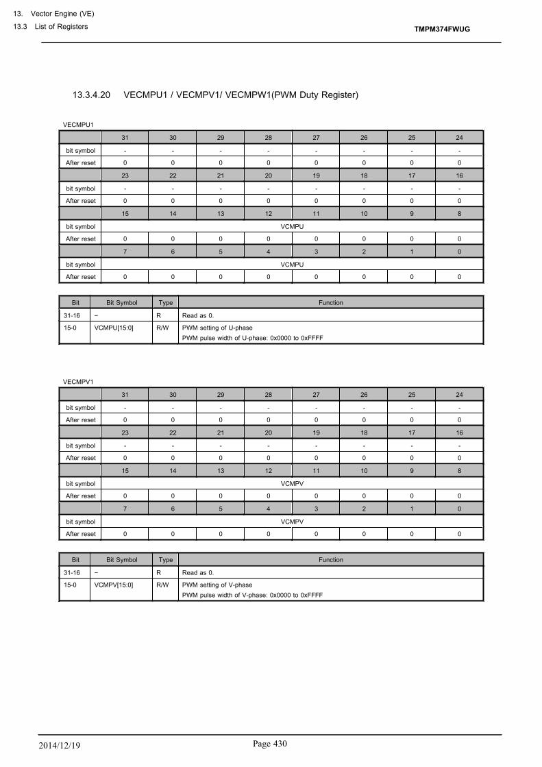
13.3.4.20 VECMPU1 / VECMPV1/ VECMPW1(PWM Duty Register)
VECMPU1
31 30 29 28 27 26 25 24
bit symbol - - - - - - - -
After reset 0 0 0 0 0 0 0 0
23 22 21 20 19 18 17 16
bit symbol - - - - - - - -
After reset 0 0 0 0 0 0 0 0
15 14 13 12 11 10 9 8
bit symbol VCMPU
After reset 0 0 0 0 0 0 0 0
7 6 5 4 3 2 1 0
bit symbol VCMPU
After reset 0 0 0 0 0 0 0 0
Bit Bit Symbol Type Function
31-16 − R Read as 0.
15-0 VCMPU[15:0] R/W PWM setting of U-phasePWM pulse width of U-phase: 0x0000 to 0xFFFF
VECMPV1
31 30 29 28 27 26 25 24
bit symbol - - - - - - - -
After reset 0 0 0 0 0 0 0 0
23 22 21 20 19 18 17 16
bit symbol - - - - - - - -
After reset 0 0 0 0 0 0 0 0
15 14 13 12 11 10 9 8
bit symbol VCMPV
After reset 0 0 0 0 0 0 0 0
7 6 5 4 3 2 1 0
bit symbol VCMPV
After reset 0 0 0 0 0 0 0 0
Bit Bit Symbol Type Function
31-16 − R Read as 0.
15-0 VCMPV[15:0] R/W PWM setting of V-phasePWM pulse width of V-phase: 0x0000 to 0xFFFF
TMPM374FWUG
13. Vector Engine (VE)
13.3 List of Registers
Page 4302014/12/19

VECMPW1
31 30 29 28 27 26 25 24
bit symbol - - - - - - - -
After reset 0 0 0 0 0 0 0 0
23 22 21 20 19 18 17 16
bit symbol - - - - - - - -
After reset 0 0 0 0 0 0 0 0
15 14 13 12 11 10 9 8
bit symbol VCMPW
After reset 0 0 0 0 0 0 0 0
7 6 5 4 3 2 1 0
bit symbol VCMPW
After reset 0 0 0 0 0 0 0 0
Bit Bit Symbol Type Function
31-16 − R Read as 0.
15-0 VCMPW[15:0] R/W PWM setting of W-phasePWM pulse width of W-phase: 0x0000 to 0xFFFF
TMPM374FWUG
Page 431 2014/12/19
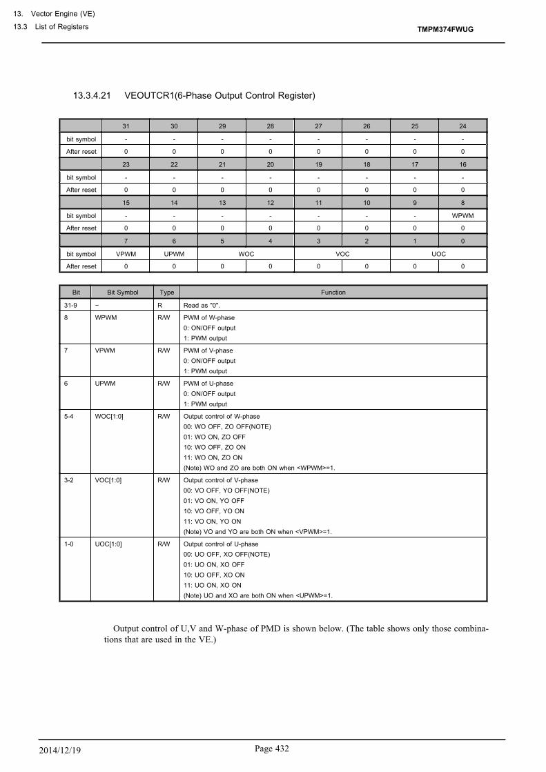
13.3.4.21 VEOUTCR1(6-Phase Output Control Register)
31 30 29 28 27 26 25 24
bit symbol - - - - - - - -
After reset 0 0 0 0 0 0 0 0
23 22 21 20 19 18 17 16
bit symbol - - - - - - - -
After reset 0 0 0 0 0 0 0 0
15 14 13 12 11 10 9 8
bit symbol - - - - - - - WPWM
After reset 0 0 0 0 0 0 0 0
7 6 5 4 3 2 1 0
bit symbol VPWM UPWM WOC VOC UOC
After reset 0 0 0 0 0 0 0 0
Bit Bit Symbol Type Function
31-9 − R Read as "0".
8 WPWM R/W PWM of W-phase0: ON/OFF output1: PWM output
7 VPWM R/W PWM of V-phase0: ON/OFF output1: PWM output
6 UPWM R/W PWM of U-phase0: ON/OFF output1: PWM output
5-4 WOC[1:0] R/W Output control of W-phase00: WO OFF, ZO OFF(NOTE)01: WO ON, ZO OFF10: WO OFF, ZO ON11: WO ON, ZO ON(Note) WO and ZO are both ON when <WPWM>=1.
3-2 VOC[1:0] R/W Output control of V-phase00: VO OFF, YO OFF(NOTE)01: VO ON, YO OFF10: VO OFF, YO ON11: VO ON, YO ON(Note) VO and YO are both ON when <VPWM>=1.
1-0 UOC[1:0] R/W Output control of U-phase00: UO OFF, XO OFF(NOTE)01: UO ON, XO OFF10: UO OFF, XO ON11: UO ON, XO ON(Note) UO and XO are both ON when <UPWM>=1.
Output control of U,V and W-phase of PMD is shown below. (The table shows only those combina-tions that are used in the VE.)
TMPM374FWUG
13. Vector Engine (VE)
13.3 List of Registers
Page 4322014/12/19

<UPWM>, <UOC> PMD setting: Output control of U-phase (UO,XO)
Setting Output
<UPWM> <UOC> UO XO
0 00 OFF output OFF output
1 00PWMU inverted
outputPWMU output
1 11 PWMU outputPWMU inverted
output
<VPWM>,<VOC> PMD setting: Output control of V-phase (VO,YO)
Setting Output
<VPWM> <VOC> VO YO
0 00 OFF output OFF output
1 00PWMV inverted
outputPWMV output
1 11 PWMV outputPWMV inverted
output
<WPWM>,<WOC> PMD setting: Output control of W-phase (WO,ZO)
Setting Output
<WPWM> <WOC> WO ZO
0 00 OFF output OFF output
1 00 PWMW invertedoutput PWMW output
1 11 PWMW output PWMW invertedoutput
13.3.4.22 VETRGCRC1(Synchronizing trigger correction value Register)
31 30 29 28 27 26 25 24
bit symbol - - - - - - - -
After reset 0 0 0 0 0 0 0 0
23 22 21 20 19 18 17 16
bit symbol - - - - - - - -
After reset 0 0 0 0 0 0 0 0
15 14 13 12 11 10 9 8
bit symbol TRGCRC
After reset 0 0 0 0 0 0 0 0
7 6 5 4 3 2 1 0
bit symbol TRGCRC
After reset 0 0 0 0 0 0 0 0
Bit Bit Symbol Type Function
31-16 − R Read as "0".
15-0 TRGCRC[15:0] R/W Used to correct the synchronizing trigger timing.The value to be set is: Correction time[s] ÷ PWM counter clock frequency[s]
TMPM374FWUG
Page 433 2014/12/19

13.3.4.23 VETRGCMP01/VETRGCMP11(Trigger timing setting Register)
VETRGCMP01
31 30 29 28 27 26 25 24
bit symbol - - - - - - - -
After reset 0 0 0 0 0 0 0 0
23 22 21 20 19 18 17 16
bit symbol - - - - - - - -
After reset 0 0 0 0 0 0 0 0
15 14 13 12 11 10 9 8
bit symbol VTRGCMP0
After reset 0 0 0 0 0 0 0 0
7 6 5 4 3 2 1 0
bit symbol VTRGCMP0
After reset 0 0 0 0 0 0 0 0
Bit Bit Symbol Type Function
31-16 − R Read as 0.
15-0 VTRGCMP0[15:0] R/W PMD setting: Specifies the trigger timing for sampling ADC in synchronization with PMD.0x0000: Prohibited0x0001 to (<MDPRD[15:0]> value -1): Trigger timing<MDPRD[15:0]> value to 0xFFFF: Prohibited
VETRGCMP11
31 30 29 28 27 26 25 24
bit symbol - - - - - - - -
After reset 0 0 0 0 0 0 0 0
23 22 21 20 19 18 17 16
bit symbol - - - - - - - -
After reset 0 0 0 0 0 0 0 0
15 14 13 12 11 10 9 8
bit symbol VTRGCMP1
After reset 0 0 0 0 0 0 0 0
7 6 5 4 3 2 1 0
bit symbol VTRGCMP1
After reset 0 0 0 0 0 0 0 0
Bit Bit Symbol Type Function
31-16 − R Read as 0.
15-0 VTRGCMP1[15:0] R/W PMD setting: Specifies the trigger timing for sampling ADC in synchronization with PMD.0x0000: Prohibited0x0001 to (<MDPRD[15:0]> value -1): Trigger timing<MDPRD[15:0]> value to 0xFFFF: Prohibited
Note 1: These registers are effective when one of the following PMD trigger modes is selected: count-downmatch, count-up match, count-up/-down match.
Note 2: These registers are ineffective when the PMD trigger output mode is set to trigger select output(PMD1TRGMD<TRGOUT>=1).
TMPM374FWUG
13. Vector Engine (VE)
13.3 List of Registers
Page 4342014/12/19
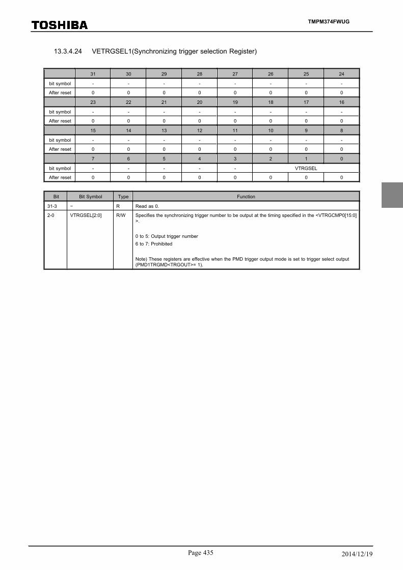
13.3.4.24 VETRGSEL1(Synchronizing trigger selection Register)
31 30 29 28 27 26 25 24
bit symbol - - - - - - - -
After reset 0 0 0 0 0 0 0 0
23 22 21 20 19 18 17 16
bit symbol - - - - - - - -
After reset 0 0 0 0 0 0 0 0
15 14 13 12 11 10 9 8
bit symbol - - - - - - - -
After reset 0 0 0 0 0 0 0 0
7 6 5 4 3 2 1 0
bit symbol - - - - - VTRGSEL
After reset 0 0 0 0 0 0 0 0
Bit Bit Symbol Type Function
31-3 − R Read as 0.
2-0 VTRGSEL[2:0] R/W Specifies the synchronizing trigger number to be output at the timing specified in the <VTRGCMP0[15:0]>. 0 to 5: Output trigger number6 to 7: Prohibited Note) These registers are effective when the PMD trigger output mode is set to trigger select output(PMD1TRGMD<TRGOUT>= 1).
TMPM374FWUG
Page 435 2014/12/19

13.3.4.25 VEEMGRS1(EMG return control Register)
31 30 29 28 27 26 25 24
bit symbol - - - - - - - -
After reset 0 0 0 0 0 0 0 0
23 22 21 20 19 18 17 16
bit symbol - - - - - - - -
After reset 0 0 0 0 0 0 0 0
15 14 13 12 11 10 9 8
bit symbol - - - - - - - -
After reset 0 0 0 0 0 0 0 0
7 6 5 4 3 2 1 0
bit symbol - - - - - - - EMGRS
After reset 0 0 0 0 0 0 0 0
Bit Bit Symbol Type Function
31-1 − R Read as "0".
0 EMGRS R/W PMD setting : EMG return command for returning from the EMG state0: Nop1: EMG return command
TMPM374FWUG
13. Vector Engine (VE)
13.3 List of Registers
Page 4362014/12/19

13.4 Description of Operations
13.4.1 Schedule Management
Figure 13-4 shows a flowchart for motor control. The Vector Engine makes state transitions according tothe schedule and mode settings which are programmed through the relevant registers.
RESET
Initial settingVE/PMD/ADC
Enable VE
Change VEACTSCH
Change VEACTSCHChange VEMODE
Change VEACTSCHChange VEMODE
Change VEACTSCH
Change VEACTSCHChange VEMODE
Change VEACTSCHChange VEMODE
Change VEMODE
ChangeVEMODE
Executed by the VE
Software control
Stop
Positioning
Forcedcommutation
Speed control bycurrent feedback
Brake
EMG return
Initial input
Figure 13-4 Example of Motor Control Flow
RESET : Microcontroller reset
Initial setting : Initial setting by a user-created program
Stop : Stop the motor.
Initial input : Sample and store zero-current data when the motor is at stop
Positioning : Determine the initial motor position.
Forced commutation : Start the motor. For a specified period, the motor is rotated at a speci-fied speed, not controlled by current feedback.
Speed control bycurrent feedback
: Control motor rotation by current feedback.
Brake : Deceleration control
EMG return : Return from the EMG state.
TMPM374FWUG
Page 437 2014/12/19

13.4.1.1 Schedule Control
The VEACTSCH register is used to select the schedule to be executed.
A schedule is comprised of an output schedule handling output-related tasks and an input schedule han-dling input-related tasks. Table 13-1 shows the tasks that are executed in each schedule.
The VEMODE register is used to enable or disable phase interpolation, control output operation, and en-able or disable zero-current detection as appropriate for each step of the motor control flow (see Table13-2).
Table 13-1 Tasks To Be Executed in Each Schedule
Schedule Selection
VEACTSCH
Output Schedule Input Schedule
Currentcontrol
SIN/COScomputation
Outputcoordinate
axisconversion
Outputphase
conversion
Outputcontrol
Triggergeneration
Inputprocessing
Inputphase
conversion
Inputcoordinate
axisconversion
0 : Individual execu-tion (Note1) (Note1) (Note1) (Note1) (Note1) (Note1) (Note1) (Note1) (Note1)
1 : Schedule 1 ο ο (Note2) ο ο ο (Note3) ο ο (Note4) ο ο
4 : Schedule 4 - ο (Note2) ο ο ο (Note3) ο ο (Note4) ο ο
9 : Schedule 9 - - - - ο (Note3) ο ο (Note4) - -
ο: A task that is executed according to the schedule.−: A task that is independent of the schedule.
Note 1: Each task is executed only when it is specified.Note 2: Phase interpolation.Note 3: Output OFF: <EMGRS>Note 4: Task operation to be switched by zero-current detection.
Table 13-2 Typical Setting Example
Register SettingSchedule selection
VEACTSCHTask specification
VETASKAPPPhase interpolation
VEMODEOutput control
VEMODE
Zero-currentdetectionVEMODE
Motor Control Flow <VACTB[3:0]> <VTASKB[3:0]> <PVIEN> <OCRMD[1:0]> <ZIEN>
Stop 9 0 x 00 0
Initial input 9 0 x 00 1
Positioning 1 5 0 01 0
Forced commutation 1 5 1 01 0
Speed controlby current feedback
1 5 1 01 0
Brake 4 6 0 01 0
EMG return 9 0 x 11 0
An output schedule begins executing by the VECPURUNTRG command. When all output-relatedtasks are completed, the Vector Engine enters a standby state and waits for a start trigger for input-rela-ted tasks. At this time, schedules of the other channel can be executed.
An input schedule begins executing by a start trigger. When all input-related tasks are completed, the Vec-tor Engine generates an interrupt to the CPU and enters a halt state. However, if the schedule has its re-peat count (VEREPTIME) set to "2" or more, an interrupt is not generated until the schedule is executedthe specified number of times.
TMPM374FWUG
13. Vector Engine (VE)
13.4 Description of Operations
Page 4382014/12/19
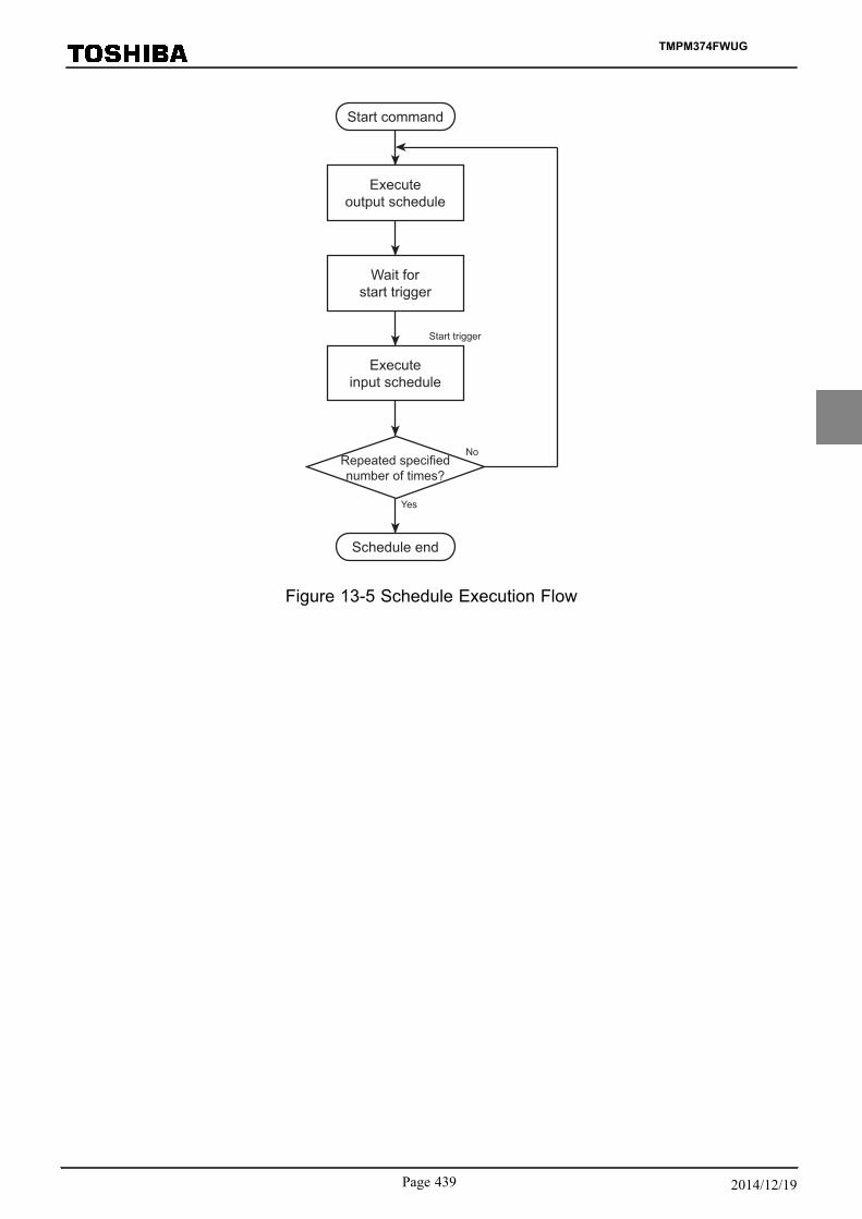
Start command
Executeoutput schedule
Wait forstart trigger
Executeinput schedule
Repeated specifiednumber of times?
Schedule end
Yes
No
Start trigger
Figure 13-5 Schedule Execution Flow
TMPM374FWUG
Page 439 2014/12/19

13.4.1.2 Start Control
Enable the Vector Engine with the VEEN register. Specify a schedule (VEACTSCH register), task tobe executed (VETASKAPP register) and repeat count (VEREPTIME register).
A schedule of the Vector Engine is comprised of an output schedule and an input schedule. Typically,the Vector Engine executes an output schedule first, enters a standby state, and then starts executing an in-put schedule by a start trigger.
The output schedule and the input it are started by following conditions.
・ An output schedule is started:
1. By the VECPURUNTRG command. In this case, the task specified in the VETASKAPPregister is executed.
2. On a repeat start (when VEREPTIME ≥ 2) after the corresponding input schedule is com-pleted.
・ An input schedule is started:
1. By a start trigger (selected in the VETRGMODE register) after the corresponding outputschedule is completed.
2. By the VECPURUNTRG command. In this case, the task specified in the VETASKAPPregister is executed.
13.4.2 Summary of Tasks
Table 13-3 gives a summary of tasks executed in output and input schedules.
When each task is to be executed individually or specified as a startup task, use the task number shown inthis table.
Table 13-3 List of Tasks
Task Task Description Task Number
Outputschedule
Current control Controls dq currents 5
SIN/COS computa-tion
Performs sine/cosine computation and-phase interpolation. 6
Output coordinateaxis conversion Converts dq coordinates to αβ coordinates. 7
Output phase con-version Converts 2-phase to 3-phase. 8
Output controlConverts data to PMD setting format.Switches PWM shift.
0
Trigger generation Generates synchronization trigger timing. 1
Inputschedule
Input processing Captures AD conversion results and con-verts them into fixed-point format. 2
Input phase conver-sion Converts 3-phase to 2-phase. 3
Input coordinate ax-is conversion Converts αβ coordinates to dq coordinates. 4
TMPM374FWUG
13. Vector Engine (VE)
13.4 Description of Operations
Page 4402014/12/19

13.4.2.1 Current Control
The current control unit is comprised of a PI control unit for d-axis and a PI control unit for q-axis,and calculates d-axis and q-axis voltages.
1. PI control of d-axis current
<Equations>
Δ ID = VEIDREF1 − <ID[31:0]> : Difference between current reference value andcurrent feedback
VDI1 = VECIDKI1 × Δ ID + VDI1 : Integral term computation
VEVD1 = VECIDKP1 × Δ ID + VDI1 : Voltage calculation using proportional term
Register Name Function
Input
VEID1 d-axis current 32-bit fixed-point data (31 fractional bits)
VEIDREF1 eference value of d-axis current 16-bit fixed-point data (15 fractional bits)
VECIDKP1 Proportional coeffi-cient 16-bit data
VECIDKI1 Integral coefficient 16-bit data
Output VEVD1 d-axis voltage 32-bit fixed-point data (31 fractional bits)
Internal VDI1 Integral term of d-ax-is voltage 64-bit fixed-point data (63 fractional bits)
2. PI control of q-axis current
<Equations>
Δ IQ = VEIQREF1 − <IQ[31:0]> : Difference between current reference value andcurrent feedback
VQI1 = VECIQKI1 × Δ IQ + VQI1 : Integral term computation
VEVQ1 = VECIQKP1 × Δ IQ + VQI1 : Voltage calculation using proportional term
Register Name Function
Input
VEIQ1 q-axis current 32-bit fixed-point data (31 fractional bits)
VEIQREF1 Reference value ofq-axis current 16-bit fixed-point data (15 fractional bits)
VECIQKP1 Proportional coeffi-cient 16-bit data
VECIQKI1 Integral coefficient 16-bit data
Output VEVQ1 q-axis voltage 32-bit fixed-point data (31 fractional bits)
Internal VQI1 Integral term of q-ax-is voltage 64-bit fixed-point data (63 fractional bits)
TMPM374FWUG
Page 441 2014/12/19

13.4.2.2 SIN/COS Computation
The SIN/COS computation unit is comprised of a phase interpolation unit and a SIN/COS computationunit.
Phase interpolation calculates the rotation speed by integrating with the PWM period. It is executed on-ly when phase interpolation is enabled.
1. Phase interpolation
<Equations>
VETHETA1 = VEOMEGA1 × VETPWM1 + VETHETA1: Integration of rotation speed.Only when phase interpolation is en-abled.
Register Name Function
Input
VETHETA1 Phase θ 16-bit fixed-point data (0.0 to1.0, 16 fractional bits)
VEOMEGA1 Rotation speed 16-bit fixed-point data (-1.0 to 1.0, 15 fractional bits)
VETPWM1 PWM period rate 16-bit fixed-point data (0.0 to1.0, 16 fractional bits)
VEMODE1 Phase interpolationenable Mode settings
Output VETHETA1 Phase θ 16-bit fixed-point data (0.0 to 1.0, 16 fractional bits)
2. SIN/COS computation
<Equations>
VESINM1 = VESIN1 : Saves previous value (for inputprocessing).
VECOSM1 = VECOS1 : Saves previous value (for inputprocessing).
VESIN1 = sin ( VETHETA1 × π ) : SIN/COS computation
VECOS1 = sin ( ( VETHETA1 + 1/4 ) × π ) : SIN/COS computation
レジスタ名 Function
Input VETHETA1 Phase θ 16-bit fixed-point data (0.0 to 1.0, 16 fractional bits)
OUTPUT
VESIN1 Sine value at θ
16-bit fixed-point data (-1.0 to 1.0, 15 fractional bits)VECOS1 Cosine value at θ
VESINM1 Previous sine value
VECOSM1 Previous cosine val-ue
TMPM374FWUG
13. Vector Engine (VE)
13.4 Description of Operations
Page 4422014/12/19

13.4.2.3 Output Voltage Conversion (Coordinate axis Conversion/Phase Conversion)
Output voltage conversion is comprised of dq-to-αβ coordinate axis conversion and 2-phase-to-3-phaseconversion.
The dq-to-αβ coordinate axis conversion calculates Vα,Vβ from Vd, Vq in SIN and COS.
The 2-phase-to-3-phase conversion performs segmentation by using Vα and Vβ and performs space vec-tor conversion to calculate Va, Vb and Vc.
For the 2-phase-to-3-phase conversion, either 2-phase modulation or 3-phase modulation can be selected.
1. dq-to-αβ coordinate conversion
<Equations>
VETMPREG3 = VECOS1 × VEVD1 − VESIN1 × VEVQ1 : Calculates Vα.
VETMPREG4 = VESIN1 × VEVD1 + VECOS1 × VEVQ1 : Calculates Vβ.
Register Name Function
INPUT
VEVD1 d-axis voltage 32-bit fixed-point data (-1.0 to 1.0, 31 fractional bits)
VEVQ1 q-axis voltage 32-bit fixed-point data (-1.0 to 1.0, 31 fractional bits)
VESIN1 Sine value at θ 16-bit fixed-point data (-1.0 to 1.0, 15 fractional bits)
VECOS1 Cosine value at θ 16-bit fixed-point data (-1.0 to 1.0, 15 fractional bits)
OUTPUTVETMPREG3 α−axis voltage 32-bit fixed-point data (-1.0 to 1.0, 31 fractional bits)
VETMPREG4 β−axis voltage 32-bit fixed-point data (-1.0 to 1.0, 31 fractional bits)
TMPM374FWUG
Page 443 2014/12/19
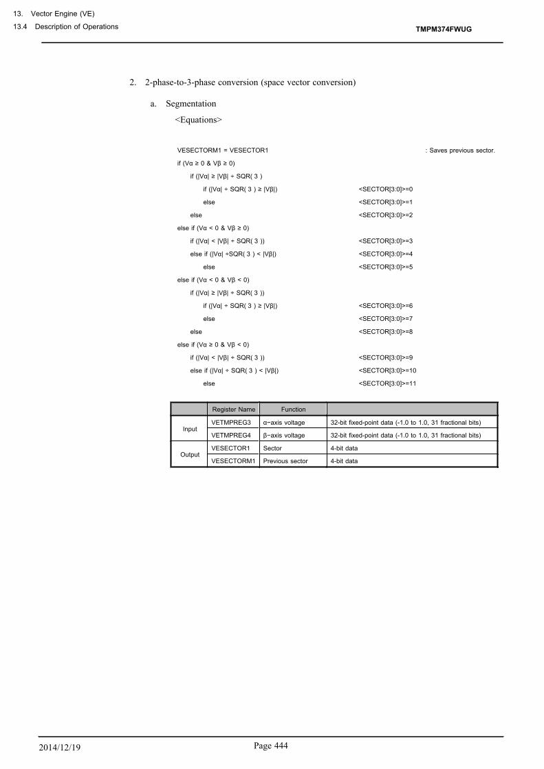
2. 2-phase-to-3-phase conversion (space vector conversion)
a. Segmentation
<Equations>
VESECTORM1 = VESECTOR1 : Saves previous sector.
if (Vα ≥ 0 & Vβ ≥ 0)
if (|Vα| ≥ |Vβ| ÷ SQR( 3 )
if (|Vα| ÷ SQR( 3 ) ≥ |Vβ|) <SECTOR[3:0]>=0
else <SECTOR[3:0]>=1
else <SECTOR[3:0]>=2
else if (Vα < 0 & Vβ ≥ 0)
if (|Vα| < |Vβ| ÷ SQR( 3 )) <SECTOR[3:0]>=3
else if (|Vα| ÷SQR( 3 ) < |Vβ|) <SECTOR[3:0]>=4
else <SECTOR[3:0]>=5
else if (Vα < 0 & Vβ < 0)
if (|Vα| ≥ |Vβ| ÷ SQR( 3 ))
if (|Vα| ÷ SQR( 3 ) ≥ |Vβ|) <SECTOR[3:0]>=6
else <SECTOR[3:0]>=7
else <SECTOR[3:0]>=8
else if (Vα ≥ 0 & Vβ < 0)
if (|Vα| < |Vβ| ÷ SQR( 3 )) <SECTOR[3:0]>=9
else if (|Vα| ÷ SQR( 3 ) < |Vβ|) <SECTOR[3:0]>=10
else <SECTOR[3:0]>=11
Register Name Function
InputVETMPREG3 α−axis voltage 32-bit fixed-point data (-1.0 to 1.0, 31 fractional bits)
VETMPREG4 β−axis voltage 32-bit fixed-point data (-1.0 to 1.0, 31 fractional bits)
OutputVESECTOR1 Sector 4-bit data
VESECTORM1 Previous sector 4-bit data
TMPM374FWUG
13. Vector Engine (VE)
13.4 Description of Operations
Page 4442014/12/19

b. 3-phase voltage calculation (when 3-phase modulation is selected and <SECTOR[3:0]>=0 )
<Equations>
: Calculates V1 period.
: Calculates V2 period.
t3 = 1 − t1 − t2 : Calculates V0+V7 period.
VETMPREG0 = t1 + t2 + t3 ÷ 2 : Calculates Va.
VETMPREG1 = t2 + t3 ÷ 2 : Calculates Vb.
VETMPREG2 = t3 ÷ 2 : Calculates Vc.
Register Name Function
Input
VETMPREG3 α−axis voltage 32-bit fixed-point data (-1.0 to 1.0, 31 fractional bits)
VETMPREG4 β−axis voltage 32-bit fixed-point data (-1.0 to 1.0, 31 fractional bits)
VEVDC1 Supply voltage 16-bit fixed-point data (0.0 to 1.0, 15 fractional bits)
VESECTOR1 Sector 4-bit data
VEFMODE1 Modulation mode Mode settings
Output
VETMPREG0 a-phase voltage 32-bit fixed-point data (0.0 to 1.0, 31 fractional bits)
VETMPREG1 b-phase voltage 32-bit fixed-point data (0.0 to 1.0, 31 fractional bits)
VETMPREG2 c-phase voltage 32-bit fixed-point data (0.0 to 1.0, 31 fractional bits)
TMPM374FWUG
Page 445 2014/12/19

13.4.2.4 Output Control
The output control unit converts 3-phase voltage values into PWM setting format (VECMPU1,VECMPV1 and VECMPW1 ), and sets the VEOUTCR1 register to control output operation.
When 1-shunt current detection and 2-phase modulation are selected and PWM is enabled, if the rota-tion speed is slower than the PWM shift switching reference value, output is switched to shift PWM output.
Register Name Function
Input
VETMPREG0 a-phase voltage 32-bit fixed-point data (0.0 to 1.0, 31 fractional bits)
VETMPREG1 b-phase voltage 32-bit fixed-point data (0.0 to 1.0, 31 fractional bits)
VETMPREG2 c-phase voltage 32-bit fixed-point data (0.0 to 1.0, 31 fractional bits)
VEMDPRD1 PWM period 16-bit data (PMD PWM period )
VESECTOR1 Sector 4-bit data
VEOMEGA1 Rotation speed 16-bit fixed-point data (-1.0 to 1.0, 15 fractional bits)
VEFPWMCHG1 PWM shift switching reference 16-bit fixed-point data (-1.0 to 1.0, 15 fractional bits)
VEMODE1 Output control operation Mode settings
VEFMODE1PMD channel/ shift enable/modulation mode/detection mode/
Mode settings
Output
VECMPU1 PMD U-phase PMW setting 16- bit data (0 to MDPRD value)
VECMPV1 PMD V-phase PWM setting 16- bit data (0 to MDPRD value)
VECMPW1 PMD W-phase PWM setting 16- bit data (0 to MDPRD value)
VEOUTCR1 PMD output control setting 9-bit setting
VEEMGRS1 PMD EMG return 1-bit setting
VEMCTLF1 Shift switching flag Status
TMPM374FWUG
13. Vector Engine (VE)
13.4 Description of Operations
Page 4462014/12/19

13.4.2.5 Trigger Generation
The trigger generation unit calculates the trigger timing from the PWM setting values (VECMPU1,VECMPV1 and VECMPW1) as appropriate to the current detection method, and sets the VETRGCMP01and VETRGCMP11 registers.
Register Name Function
Input
VECMPU1 PMD U-phase PWM setting 16-bit data (0 to MDPRD value)
VECMPV1 PMD V-phase PWM setting 16-bit data (0 to MDPRD value)
VECMPW1 PMD W-phase PWM setting 16-bit data (0 to MDPRD value)
VEMDPRD1 PWM period setting 16-bit data (PMD PWM period)
VETADC AD conversion time 16-bit data (0 to MDPRD value)
VETRGCRC1 Trigger correction value 16-bit data (0 to MDPRD value)
VESECTOR1 Sector 4-bit data
VEMODE1 Output control operation Mode settings
VEFMODE1PMD channel/ shift enable/modulation mode/detection mode
Mode settings
VEMCTLF1 Shift switching flag Status
Output
VETRGCMP0 PMD trigger 0 timing 16-bit data (0 to MDPRD value)
VETRGCMP1 PMD trigger 1 timing 16-bit data (0 to MDPRD value)
VETRGSEL1 PMD trigger selection 3-bit data
TMPM374FWUG
Page 447 2014/12/19

13.4.2.6 Input Processing
The input processing unit saves segmented 3-phase current conversion results, and converts the currentand voltage conversion results into fixed-point data. It saves zero-current conversion results in the initial in-put processing.
Register Name Function
VEADREG0B ADC unit B conversion result 0
16-bit data (The upper 12 bits are used.) VEADREG1B ADC unit B conversion result 1
VEADREG2B ADC unit B conversion result 2
Input VEADREG3B ADC unit B conversion result 3
VEPHNUM0B ADREG0B detected phase infor-mation
2-bit data VEPHNUM1B ADREG1B detected phase infor-
mation
VEPHNUM2B ADREG2B detected phase infor-mation
VEPHNUM3B ADREG3B detected phase infor-mation
VESECTORM1 Sector information 4-bit data
VEMODE1 Zero-current detection Mode settings
VEFMODE1PMD channel /current detection mode /ADC unit /shift enable
Mode settings
VEMCTLF1 Shift switching flag Status
Output
VEVDC1 Supply voltage 16-bit fixed-point data (0.0 to 1.0, 15 fractional bits)
VETMPREG0 a-phase current
32-bit fixed-point data (-1.0 to 1.0, 31 fractional bits)VETMPREG1 b-phase current
VETMPREG2 c-phase current
Internal
VEIAO1 a-phase zero-current conversionresult
16-bit data (The upper 12 bits are used.)VEIBO1 b-phase zero-current conversionresult
VEICO1 c-phase zero-current conversionresult
VEIAADC1 a-phase current conversion result
16-bit data (The upper 12 bits are used.)VEIBADC1 b-phase current conversion result
VEICADC1 c-phase current conversion result
TMPM374FWUG
13. Vector Engine (VE)
13.4 Description of Operations
Page 4482014/12/19
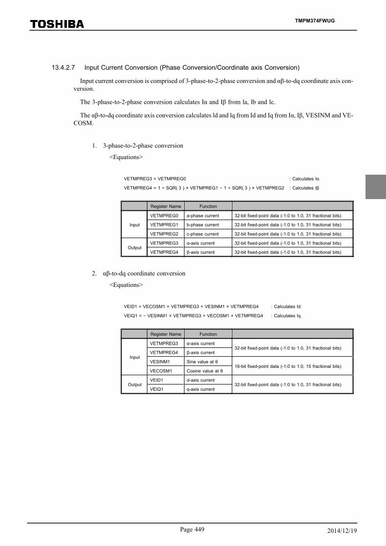
13.4.2.7 Input Current Conversion (Phase Conversion/Coordinate axis Conversion)
Input current conversion is comprised of 3-phase-to-2-phase conversion and αβ-to-dq coordinate axis con-version.
The 3-phase-to-2-phase conversion calculates Iα and Iβ from la, lb and lc.
The αβ-to-dq coordinate axis conversion calculates ld and lq from Id and Iq from Iα, Iβ, VESINM and VE-COSM.
1. 3-phase-to-2-phase conversion
<Equations>
VETMPREG3 = VETMPREG0 : Calculates Iα.
VETMPREG4 = 1 ÷ SQR( 3 ) × VETMPREG1 − 1 ÷ SQR( 3 ) × VETMPREG2 : Calculates Iβ
Register Name Function
Input
VETMPREG0 a-phase current 32-bit fixed-point data (-1.0 to 1.0, 31 fractional bits)
VETMPREG1 b-phase current 32-bit fixed-point data (-1.0 to 1.0, 31 fractional bits)
VETMPREG2 c-phase current 32-bit fixed-point data (-1.0 to 1.0, 31 fractional bits)
OutputVETMPREG3 α-axis current 32-bit fixed-point data (-1.0 to 1.0, 31 fractional bits)
VETMPREG4 β-axis current 32-bit fixed-point data (-1.0 to 1.0, 31 fractional bits)
2. αβ-to-dq coordinate conversion
<Equations>
VEID1 = VECOSM1 × VETMPREG3 + VESINM1 × VETMPREG4 : Calculates Id.
VEIQ1 = − VESINM1 × VETMPREG3 + VECOSM1 × VETMPREG4 : Calculates Iq.
Register Name Function
Input
VETMPREG3 α-axis current32-bit fixed-point data (-1.0 to 1.0, 31 fractional bits)
VETMPREG4 β-axis current
VESINM1 Sine value at θ16-bit fixed-point data (-1.0 to 1.0, 15 fractional bits)
VECOSM1 Cosine value at θ
OutputVEID1 d-axis current
32-bit fixed-point data (-1.0 to 1.0, 31 fractional bits)VEIQ1 q-axis current
TMPM374FWUG
Page 449 2014/12/19

13.5 Combinations of the VE Channel and ADC Unit
The Vector Engine calculates the stored value in AD conversion result register 0 to 2 (ADBREG0 to 2) as a cur-rent data and calculates the sotred value in AD conversion result register 3 (ADBREG3) as a voltage data. There-fore, please specify it with proper setting, referring to Table 13-4.
Table 13-4 Combination of VE and ADC
Vector Engine ADC Unit B
Currentditection
<IDMODE[1:0]>ADREG0 ADREG1 ADREG2 ADREG3
0xCurrentdata 1
Currentdata 2
Note 1 VDC data
1xCurrentdata 1
Currentdata 2
VDC data
Note 1: Specifying the phase information to the register is necessary. However the AD conversion result of its register is notused for calculation.
TMPM374FWUG
13. Vector Engine (VE)
13.5 Combinations of the VE Channel and ADC Unit
Page 4502014/12/19
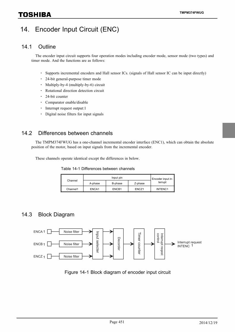
14. Encoder Input Circuit (ENC)
14.1 OutlineThe encoder input circuit supports four operation modes including encoder mode, sensor mode (two types) and
timer mode. And the functions are as follows:
・ Supports incremental encoders and Hall sensor ICs. (signals of Hall sensor IC can be input directly)・ 24-bit general-purpose timer mode・ Multiply-by-4 (multiply-by-6) circuit・ Rotational direction detection circuit・ 24-bit counter・ Comparator enable/disable・ Interrupt request output:1・ Digital noise filters for input signals
14.2 Differences between channelsThe TMPM374FWUG has a one-channel incremental encoder interface (ENC1), which can obtain the absolute
position of the motor, based on input signals from the incremental encoder.
These channels operate identical except the differences in below.
Table 14-1 Differences between channels
ChannelInput pin Encoder input in-
terruptA-phase B-phase Z-phase
Channel1 ENCA1 ENCB1 ENCZ1 INTENC1
14.3 Block Diagram
Noise filter
Noise filter
Noise filter
ENCA
ENCB
ENCZ
Input selecter
Decorder
Timer counter
Interrupt reqestcontrol Interrupt request
INTENC 1
1
1
1
Figure 14-1 Block diagram of encoder input circuit
TMPM374FWUG
Page 451 2014/12/19
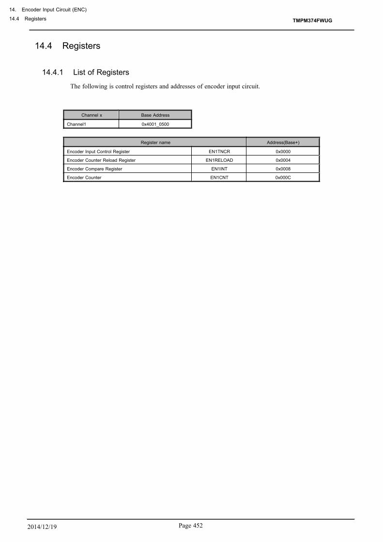
14.4 Registers
14.4.1 List of Registers
The following is control registers and addresses of encoder input circuit.
Channel x Base Address
Channel1 0x4001_0500
Register name Address(Base+)
Encoder Input Control Register EN1TNCR 0x0000
Encoder Counter Reload Register EN1RELOAD 0x0004
Encoder Compare Register EN1INT 0x0008
Encoder Counter EN1CNT 0x000C
TMPM374FWUG
14. Encoder Input Circuit (ENC)
14.4 Registers
Page 4522014/12/19

14.4.2 EN1TNCR(Encoder Input Control Register)
31 30 29 28 27 26 25 24
bit symbol - - - - - - - -
After reset 0 0 0 0 0 0 0 0
23 22 21 20 19 18 17 16
bit symbol - - - - - MODE P3EN
After reset 0 0 0 0 0 0 0 0
15 14 13 12 11 10 9 8
bit symbol CMP REVERR UD ZDET SFTCAP ENCLR ZESEL CMPEN
After reset 0 0 0 0 0 0 0 0
7 6 5 4 3 2 1 0
bit symbol ZEN ENRUN NR INTEN ENDEV
After reset 0 0 0 0 0 0 0 0
Bit Bit Symbol Type Function
31-19 − R Read as "0".
18-17 MODE[1:0] R/W Encoder input mode setting00:Encoder mode01:Sensor mode (event count))10:Sensor mode (timer count))11:Timer mode
16 P3EN R/W 2-phase / 3-phase input selection (sensor mode) (Note 1)0:2-phase input1:3-phase input Sets the number of input signals.
15 CMP R Compare flag0:-1:Compare (Clear by RD) If comparing is executed, <CMP> is set to "1".Flag is cleared by reading the values. When <ENRUN> = "0" is set, always "0" is set. Writing to this bitis no effect.
14 REVERR R Reverse error flag (Sensor mode (at timer count)) (Note 2)0:-1:Error (Clear by RD) In sensor mode (at timer count), when a reverse error occurs, <REVERR> is set to "1".Flag is cleared by reading the values. When <ENRUN> = "0" is set, always "0" is set.Writing to this bit is no effect.In the encoder mode, sensor mode (event count) and timer mode, this bit has no meaning.
13 UD R Rotation direction0:CCW (A-phase has the 90-degree phase lead to B-phase using incremental encoder)1:CW (A-phase has the 90-degree phase lag to B-phase using incremental encoder) <UD> is set to 1 when the CW direction is indicated. <UD> is cleared to 0 when the CCW direction is in-dicated . <UD> remains cleared while <ENRUN> = 0.
TMPM374FWUG
Page 453 2014/12/19

Bit Bit Symbol Type Function
12 ZDET R Z-Detected0:Not detected1:Z-phase detected <ZDET> is set to 1 on the first edge of Z input signal (ENCZ) after <ENRUN> is written from 0 to 1.This occurs on a rising edge of the signal Z during CW rotation or on a falling edge of Z during CCW ro-tation.<ZDET> is set to "0" when <ENRUN> = "0".<ZEN> has no influence on the value of <ZDET>.<ZDET> is set to "0" in the sensor event count and the sensor timer count modes.In the sensor mode (event count) and sensor mode (timer count), this bit is always set to "0".
11 SFTCAP W Executes software capture (timer mode/sensor mode (at timer count))0:-1:Software capture If <SFTCAP> is set to 1, the value of the encoder counter is captured into the EN1CNT register.Writing "0" to <SFTCAP> has no effect. Reading <SFTCAP> always returns to "0".In Encoder and Sensor Event Count modes, <SFTCAP> has no effect; writing "1" to this bit is ignored.
10 ENCLR W Encoder pulse counter clear0:-1:Clear Writing a 1 to <ENCLR> clears the encoder counter to "0". Once cleared, the encoder counter restartscounting from 0. Writing "0" to <ENCLR> has no effect. Reading <ENCLR> always returns to "0".
9 ZESEL R/W Edge selection of ENCZ (timer mode)0:Rising edge1:Falling edge In timer mode, this bit selects inputs edge of ENCZ used as external trigger.In the other mode, this bit has no meaning.
8 CMPEN R/W Compare enable0:Disable1:Enable When "1" is set to <CMPEN>, this bit compares counter values of encoder counter with register valueof EN1INT. When "0" is set to <CMPEN> , this compare is disabled.
7 ZEN R/W Z-phase enable (Encoder mode/timer mode)0:Disable1:Enable In the other mode, this bit has no meaning
<Encoder mode>Clear setting of encodercounter using ENCZ input
When <ZEN> = "1" is set, if a rising edge of ENCZ is detected dur-ing rotating clockwise, the encoder counter is cleared to "0".If a falling edge of ENCZ is detected during rotating counter- clock-wise, the encoder counter is cleared to "0".If the edges of ENCLK (multiply by 4 clock derived from the deco-ded A and B signals) and the edge of ENCZ coincide, the encod-er counter is cleared to "0" without incrementing or decrement-ing (i.e., the clear takes precedence).
<Timer mode>Sets ENCZ input to use asan external trigger.
When <ZEN> = 1, the value of the encoder counter is captured in-to the EN1INT register and cleared to "0" on the edge of ENCZ se-lected by <ZESEL>.
6 ENRUN R/W Encoder operation enable0:Disable1:Enable Setting <ENRUN> to 1 and clearing <ZDET> to "0" enables the encoder operation.Clearing <ENRUN> to "0" disables the encoder operation.There are counters and flags that are cleared and not cleared when <ENRUN> bit is cleared to "0".
TMPM374FWUG
14. Encoder Input Circuit (ENC)
14.4 Registers
Page 4542014/12/19

Bit Bit Symbol Type Function
5-4 NR[1:0] R/W Noise filter00:No filtering01:Filters out pulses narrower than 31/fsys as noise10:Filters out pulses narrower than 63/fsys as noise11:Filters out pulses narrower than 127/fsys as noise The digital noise filters remove pulses narrower than the width selected by <NR[1:0]>.
3 INTEN R/W Encoder interrupt enable0:Disable1:Enable <INTEN> enables or disables the ENC interrupt.Setting <INTEN> to "1" enables interrupt generation. Setting <INTEN> to "0" disables interrupt generation.
2-0 ENDEV[2:0] R/W Encoder pulse division factor000:divided by 1 100:divided by 16001:divided by 2 101:divided by 32010:divided by 4 110:divided by 64011:divided by 8 111:divided by 128 Sets encoder pulse division factorThe frequency of the encoder pulse is divided by the factor specified by <ENDEV[2:0]>. The divided sig-nal determines the interval of the event interrupt.
Note 1: In the encoder mode or timer mode, <P3EN> must be set to "0".Note 2: If changing the mode, first read the flag to clear.
TMPM374FWUG
Page 455 2014/12/19

The operation mode has eight modes specified with<MODE[1:0]>, <P3EN> and <ZEN>.
The operation mode settings are as follows:
<MODE[1:0]> <ZEN> <P3EN> Input pin Mode
000
0A, B Encoder mode
1 A,B,Z Encoder mode (use of Z)
01 00 U,V Sensor mode (event count, 2-phase input)
1 U,V,W Sensor mode (event count, 3-phase input)
10 00 U,V Sensor mode (timer count, 2-phase input)
1 U,V,W Sensor mode (timer count, 3-phase input)
110
0- Timer mode
1 Z Timer mode (use of Z)
The following is the status of <ENRUN> and corresponding signals.
Counter/flag<ENRUN> = 0
(After reset)<ENRUN> = 1
(Operating)<ENRUN> = 0
(Stopping)
<ENRUN> = 0Object flag/counter clear
procedure
Encoder counter 0x000000 Count operation Maintains a valuewhen stopping
Software clear(<ENCLR> = 1 WR)
Noise filtercounter
0y0000000 Count-up operationCount-up operation
(Always filtering)Only reset
Encoder pulsedivision counter
0x00 Count-down operation Stopped and cleared Clear when <ENRUN> = "0"
Compare flag<CMP>
0"1" is set when com-
paringClear when read.
Cleared Clear when <ENRUN> = "0"
Reverse error flag<REVERR>
0"1" is set when error
occurs.Clear when read.
Cleared Clear when <ENRUN> = "0"
Z detection flag<ZDET>
0 "1" is set when Z is de-tected. Cleared Clear when <ENRUN> = "0"
Rotation direction bit<UD>
0 "0"/"1" is set depend-ing on the direction Cleared Clear when <ENRUN> = "0"
TMPM374FWUG
14. Encoder Input Circuit (ENC)
14.4 Registers
Page 4562014/12/19

14.4.3 EN1RELOAD(Encoder Counter Reload Register)
31 30 29 28 27 26 25 24
bit symbol - - - - - - - -
After reset 0 0 0 0 0 0 0 0
23 22 21 20 19 18 17 16
bit symbol - - - - - - - -
After reset 0 0 0 0 0 0 0 0
15 14 13 12 11 10 9 8
bit symbol RELOAD
After reset 0 0 0 0 0 0 0 0
7 6 5 4 3 2 1 0
bit symbol RELOAD
After reset 0 0 0 0 0 0 0 0
Bit Bit Symbol Type Function
31-16 − R Read as "0".
15-0 RELOAD[15:0] R/W Sets the Encoder counter period (after multiplied by 4 or 6)0x0000 to 0xFFFFZ-phase is used : Sets the number of count pulses for one rotationZ-phase is not used : Sets the number of count pulses minus one for one rotation <RELOAD[15:0]> defines the encoder counter period multiplied by 4.If the encoder counter is configured as an up-counter, it increments up to the value programmed in <RE-LOAD[15:0]> and then wraps around to "0" on the next ENCLK. If the encoder counter is configured asa down-counter, it decrements to "0" and then is reloaded with the value of <RELOAD[15:0]> on thenext ENCLK.
Note 1: The RELOAD register is only used in Encoder mode.Note 2: EN1RELOAD register should be accessed with 32-bit instructions.
TMPM374FWUG
Page 457 2014/12/19
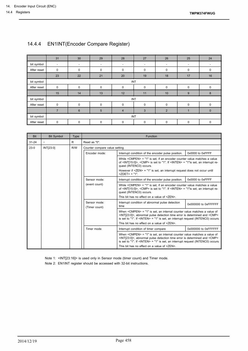
14.4.4 EN1INT(Encoder Compare Register)
31 30 29 28 27 26 25 24
bit symbol - - - - - - - -
After reset 0 0 0 0 0 0 0 0
23 22 21 20 19 18 17 16
bit symbol INT
After reset 0 0 0 0 0 0 0 0
15 14 13 12 11 10 9 8
bit symbol INT
After reset 0 0 0 0 0 0 0 0
7 6 5 4 3 2 1 0
bit symbol INT
After reset 0 0 0 0 0 0 0 0
Bit Bit Symbol Type Function
31-24 − R Read as "0".
23-0 INT[23:0] R/W Counter compare value setting
Encoder mode: Interrupt condition of the encoder pulse position. 0x0000 to 0xFFFF
While <CMPEN> = "1" is set, if an encoder counter value matches a valueof <INT[15:0]>, <CMP> is set to "1". If <INTEN> = "1"is set, an interrupt re-quest (INTENC0) occurs.However if <ZEN> = "1" is set, an interrupt request does not occur until<ZDET> = "1".
Sensor mode:(event count)
Interrupt condition of the encoder pulse position. 0x0000 to 0xFFFF
While <CMPEN> = "1" is set, if an encoder counter value matches a valueof <INT[15:0]>, <CMP> is set to "1". If <INTEN> = "1"is set, an interrupt re-quest (INTENC0) occurs.This bit has no effect on a value of <ZEN>.
Sensor mode:(Timer count)
Interrupt condition of abnormal pulse detectiontime 0x000000 to 0xFFFFFF
When <CMPEN> = "1" is set, an internal counter value matches a value of<INT[23:0]>, abnormal pulse detection time error is determined and <CMP>is set to "1". If <INTEN> = "1" is set, an interrupt request (INTENC0) occurs.This bit has no effect on a value of <ZEN>.
Timer mode Interrupt condition of timer compare 0x000000 to 0xFFFFFF
When <CMPEN> = "1" is set, an internal counter value matches a value of<INT[23:0]>, abnormal pulse detection time error is determined and <CMP>is set to "1". If <INTEN> = "1" is set, an interrupt request (INTENC0) occurs.This bit has no effect on a value of <ZEN>.
Note 1: <INT[23:16]> is used only in Sensor mode (timer count) and Timer mode.Note 2: EN1INT register should be accessed with 32-bit instructions.
TMPM374FWUG
14. Encoder Input Circuit (ENC)
14.4 Registers
Page 4582014/12/19

14.4.5 EN1CNT (Encoder Counter)
31 30 29 28 27 26 25 24
bit symbol - - - - - - - -
After reset 0 0 0 0 0 0 0 0
23 22 21 20 19 18 17 16
bit symbol CNT
After reset 0 0 0 0 0 0 0 0
15 14 13 12 11 10 9 8
bit symbol CNT
After reset 0 0 0 0 0 0 0 0
7 6 5 4 3 2 1 0
bit symbol CNT
After reset 0 0 0 0 0 0 0 0
Bit Bit Symbol Type Function
31-24 − R Read as "0".
23-0 CNT[23:0] R/W Encoder counter/capture value
Encoder mode: Counter value of encoder pulse 0x0000 to 0xFFFF
The value of encoder count can be read.In Encoder mode, the encoder counter counts up or down on each encoderpulse (ENCLK).During CW rotation, encoder counter counts up; when it has reached to thevalue of <RELOAD[15:0]>, it wraps around to "0" on the next ENCLK.During CCW rotation, encoder counter counts down; when it has reached to"0", it is reloaded with the value of <RELOAD[15:0]> on the next ENCLK.
Sensor mode:(event count)
Counter value of encoder pulse 0x0000 to 0xFFFF
The value of encoder count can be read.In Sensor Event Count mode, the encoder counter counts up or down oneach encoder pulse (ENCLK).During CW rotation, encoder counter counts up; when it has reached to"0xFFFF", it wraps around to "0" on the next ENCLK.During CCW rotation, encoder counter counts down; when it has reached to"0", it wraps around to "0xFFFF" on the next ENCLK.
Sensor mode:(Timer count)
Pulse detection time or captured value by software 0x000000 to 0xFFFFFF
The value of encoder counter can be read.In Sensor mode, the value of encoder counter can be read and captured bysoftware on each encoder pulse (ENCLK) by writing "1" to <SFTCAP>.The captured value is cleared to "0" by system reset. It can also be clearedby clearing the counter by setting <ENCLR> to 1 and then setting<SFTCAP> to 1.In Sensor Timer Count mode, the encoder counter is configured as a free-run-ning counter that counts up with fsys. The encoder counter is cleared to "0"when the encoder pulse (ENCLK) is detected. When it has reached to"0xFFFFFF", it wraps around to "0" automatically.
Timer mode Capture value of internal counter or captured val-ue by software 0x000000 to 0xFFFFFF
The value of encoder counter can be read and captured by software by writ-ing "1" to <SFTCAP>.When <ZEN> = "1", the value of the encoder counteris also captured into <CNT23:0> on the Z edge selected by <ZESEL>.The captured value is cleared to "0" by reset.It can also be cleared by clearing the counter by setting <ENCLR> to 1 andthen setting <SFTCAP> to 1.In Timer mode, the encoder counter is configured as a free-running counterthat counts up with fsys. When it has reached to "0xFFFFFF", it wrapsaround to "0" automatically.
Note 1: <CNT[23:16]> is used only in the sensor mode (Timer counting) or timer mode. In the encoder mode or sensormode (event counting), always reads as "0".
TMPM374FWUG
Page 459 2014/12/19

Note 2: EN1CNT register should be accessed with 32-bit instructions.
TMPM374FWUG
14. Encoder Input Circuit (ENC)
14.4 Registers
Page 4602014/12/19

14.5 Operational Description
14.5.1 Encoder mode
The high-speed position sensor determines the phase input from the AB encoder and the ABZ encoder.
・ Event detection (rotation pulse) → interrupt generation・ Event count → match detection interrupt generation (measures the amount of transferring)・ Detects rotation direction・ Up/down-count (changeable in operation)・ Settable counter cycle
14.5.2 Sensor mode
The low-speed position sensor determines (zero-cross determination) the phase input from UV Hall sensorand UVW Hall sensor.
There are two kinds of sensor modes such as event count mode and timer count mode (counts with fsys).
14.5.2.1 Event Count Mode
・ Event detection (rotation pulse) → interrupt generation・ Event count → match interrupt occurs (measuring the amount of transfer)・ Rotation direction detection
14.5.2.2 Timer count mode
・ Event detection (rotation pulse) → interrupt generation・ Timer count・ Rotation direction detection・ Capture function → event capture (measures event intervals) → interrupt generation
software capture・ Abnormal detection time error (timer compare) → match detection interrupt generation・ Reverse detection error → error flag caused by changing rotation direction
14.5.3 Timer mode
This mode can be used as a general-purpose 24-bit timer.
・ 24-bit up counter・ Counter clear control (software clear, timer clear, external trigger and free-run count)・ Compare function → match detection interrupt generation・ Capture function → external trigger capture → interrupt generation
software capture
TMPM374FWUG
Page 461 2014/12/19

14.6 Function
14.6.1 Mode operation outline
14.6.1.1 Encoder mode
1. If <ZEN> = 1 (<RELOAD> = 0x0380 , <EN1INT> = 0x0002)
Encorder pulse ENCLK
Encorder input A
Encorder input B
fsys
Interrupt request INTENC0
Encorder counter 110 111 112 37D 0 380 37F0 1 0
Encorder input Z
Internal Z phase detection signal
Z phase detecting <ZDET>
dir
Count clear
TIMPLS (Divided by 2)
CW
1 2 30 380 37E
CCW directionRotation direction
2. If <ZEN> = 0 (<RELOAD> = 0x0380 , <EN1INT> = 0x0002)
110 111 112 37E 37D 37C0 1 0
CW direction
1 20 380 37F
CCW direction
113
Encorder pulse ENCLK
Encorder input A
Encorder input B
fsys
Interrupt request INTENC0
Encorder counter
Encorder input Z
Internal Z phase detection signal
Z phase detecting <ZDET>
dir
Count clear
TIMPLS (Divided by 2)
Rotation direction
・ The incremental encoder inputs of the MCU should be connected to the A, B and Z channels.The encoder counter counts pulses of ENCLK, which is multiplied by 4 clock derived fromthe decoded A and B quadrature signals.
・ During CW rotation (i.e., A has the 90-degree phase lead to B), the encoder counter countsup; when it has reached to the value of <RELOAD>, it wraps around to "0" on the next ENCLK.
・ During CCW rotation (i.e., A has the 90-degree phase lag to B), the encoder counter countsdown; when it has reached to "0x0000", it is reloaded with the value of <RELOAD> on thenext ENCLK.
TMPM374FWUG
14. Encoder Input Circuit (ENC)
14.6 Function
Page 4622014/12/19

・ Additionally, when <ZEN> = "1", the encoder counter is cleared to "0" on the rising edge ofZ during CW rotation and on the falling edge of Z during CCW rotation (at the internal Z_De-tected timing). If the ENCLK edge matches Z edge, the encoder counter is cleared to "0" with-out incrementing or decrementing.
・ When <ENCLR> is set to 1, the encoder counter is cleared to "0".・ <UD> is set to 1 during CW rotation and cleared to "0" during CCW rotation.・ TIMPLS, which is derived by dividing ENCLK by a programmed factor, can be driven out ex-
ternally.・ If <CMPEN> is set to 1, an interrupt is generated when the value of the encoder counter has
reached to the value of <EN1INT>. When <ZEN> = "1", however, an interrupt does not occurwhile <ZDET> = "0".
・ When <ZDET> and <UD> are set to "0", <ENRUN> is cleared to "0".
TMPM374FWUG
Page 463 2014/12/19

14.6.1.2 Sensor mode (event count)
1. If <P3EN> = 1 (<EN1INT> = 0x0002)
fsys
FFFC FFFD FFFF
dir
CW direction
1 2 30
CCW direction
FFFE FFFAFFFF12 0 FFFE FFFD FFFC FFFB
Encorder pulse ENCLK
Encorder input U
Encorder input V
Interrupt request INTENC0
Encorder counter
Encorder input W
Count clear
TIMPLS (Divide by 2)
Rotation direction
2. If <P3EN> = 0 (<EN1INT> = 0x0002)
FFFC FFFD FFFF
CW direction
1 2 30
CCW direction
FFFE FFFAFFFF12 0 FFFE FFFD FFFC FFFB
fsys
dir
Encorder pulse ENCLK
Encorder input U
Encorder input V
Interrupt request INTENC0
Encorder counter
Encorder input W
Count clear
TIMPLS (Divide by 2)
Rotation direction
・ The Hall sensor inputs of the MCU should be connected to the U, V and W channels. The encod-er counter counts the pulses of ENCLK, which is either multiplied by 4 clock (when <P3EN>= "0") derived from the decoded U and V signals or multiplied by 6 clock (when <P3EN> ="1") derived from the decoded U, V and W signals.
・ During CW rotation (i.e., U channel has the 90-degree phase lead to V channel; V channel hasthe 90-degree phase lead to W channel), the encoder counter counts up; when it has reachedto "0xFFFF", it wraps around to "0" on the next ENCLK.
・ During CCW rotation (i.e., U channel has the 90-degree phase lag to V channel; V channelhas the 90-degree phase lag to W), the encoder counter counts down; when it has reached to"0x0000", it wraps around to "0xFFFF" on the next ENCLK.
・ When <ENCLR> is set to 1, the internal counter is cleared to "0".・ <UD> is set to 1 during CW rotation and cleared to "0" during CCW rotation.・ TIMPLS, which is derived by dividing ENCLK by a programmed factor, can be driven out ex-
ternally.・ If <CMPEN> is set to 1, an interrupt is generated when the value of the internal counter has
reached to the value of <EN1INT>.・ When <UD> and <ENRUN> are set to "0", <UD> is cleared to "0".
TMPM374FWUG
14. Encoder Input Circuit (ENC)
14.6 Function
Page 4642014/12/19

14.6.1.3 Sensor mode (Timer count)
1. If <P3EN> = 1 (<EN1INT> = 0x0002)
Interrupt reqest INTENC0
dir
CW direction CCW direction
2 3 101 2 3 10 2 3 10 2 3
C pture register 0(ini) 3
2 3 10 2 0 21 3 0 21 3 0
33 2
21 3 0 21
Reserse error REVERR
fsys
Encorder pulse ENCLK
Encorder input U
Encorder input V
Encorder counter
Encorder input W
TIMPLS (Divide by 2)
Rotation direction
2. If <P3EN> = 0 (<EN1INT> = 0x0002)
CCW direction
2 3 101 2 3 10 2 3 10 2 3
0(ini) 3
2 3 10 2 0 21 3 0 21 3 0
33 2
21 3 0 21
Interrupt reqest INTENC0
dir
Capture register
Reserse error REVERR
fsys
Encorder pulse ENCLK
Encorder input U
Encorder input V
Encorder counter
Encorder input W
TIMPLS (Divide by 2)
Rotation directionCW direction
・ In Sensor Timer Count mode, the Hall sensor inputs of the MCU should be connected to theU, V and W channels. The encoder counter measures the interval between two contiguous pul-ses of ENCLK, which is either multiplied by 4 clock (when <P3EN> = "0") derived from the de-coded U and V signals or multiplied by 6 clock (when <P3EN> = "1") derived from the deco-ded U, V and W signals.
・ The encoder counter always counts up; it is cleared to "0" on ENCLK. When the encoder coun-ter has reached to "0xFFFFFF", it wraps around to "0".
・ When <ENCLR> is set to 1, the encoder counter is cleared to "0".・ ENCLK captures the value of the encoder counter into the EN1CNT register. The captured coun-
ter value can be read out of EN1CNT.・ Setting the software capture bit, <SFTCAP>, to 1 causes the value of the encoder counter to
be captured into the EN1CNT register. This capture operation can be performed at any time.The captured counter value can be read out of EN1CNT.
・ <UD> is set to 1 during CW rotation and cleared to "0" during CCW rotation.・ If <CMPEN> is set to 1, an interrupt is generated when the value of the encoder counter has
reached to the value of <EN1INT>.
TMPM374FWUG
Page 465 2014/12/19

・ When <ENRUN> is set to "0", <UD> is cleared to "0".・ <REVERR> is set to 1 when the rotation direction has changed. This bit is cleared to "0" on a
read.・ The value of the EN1CNT register (the captured value) is retained, regardless of the value of
<ENRUN>. The EN1CNT register is only cleared by a reset.
TMPM374FWUG
14. Encoder Input Circuit (ENC)
14.6 Function
Page 4662014/12/19

14.6.1.4 Timer mode
1. If <ZEN> = 1 (<EN1INT> = 0x0006)
CCW direction
dir
Count clear
TIMPLS (Divided by 2)
CW direction
Z phase edge selection <ZESEL>
Interrupt request INTENC0
Capture register 0(ini) B B 41
31 32 3433 35 36 3837 39 40 041 1 2 43 5 6 873 4 652 7 8 A9 B 0 21 3 4Encorder counter
compare interrupt compare interruptCapture interrupt Capture interrupt
Encorder pulse ENCLK
Encorder input A
Encorder input B
fsys
Encorder input Z
Internal Z phase detection signal
Rotation direction
2. If <ZEN> = 0 (<EN1INT> = 0x0006)
CCW directionCW direction
0(ini) A A
31 32 3433 35 36 0 13 4 652 7 8 A9 B C ED F 10
compare interrupt compare interrupt
3 4 652 7 8 A9 B C D
dir
Count clear
TIMPLS (Divided by 2)
Z phase edge selection <ZESEL>
Interrupt request INTENC0
Capture register
Encorder counter
Encorder pulse ENCLK
Encorder input A
Encorder input B
fsys
Encorder input Z
Internal Z phase detection signal
Rotation direction
・ When <ZEN> = "1", the Z input pin is used as an external trigger. When <ZEN> = "0", no ex-ternal input is used to trigger the timer.
・ The encoder counter always counts up. If <ZEN> = "1", the counter is cleared to "0" on the ris-ing edge of Z when <ZESEL> is set to "0" and a falling edge when <ZESEL> is set to "1".When the encoder counter has reached to "0xFFFFFF", it wraps around to "0".
・ When <ENCLR> is set to 1, the encoder counter is cleared to "0".・ Z-Detected causes the value of the encoder counter to be captured into the EN1CNT register.
The captured counter value can be read out of EN1CNT.
TMPM374FWUG
Page 467 2014/12/19
・ Setting the software capture bit, <SFTCAP>, to 1 causes the value of the encoder counter tobe captured into the EN1CNT register. This capture operation can be performed at any time.The captured counter value can be read out of EN1CNT.
・ <UD> is set to 1 during CW rotation and cleared to "0" during CCW rotation.・ If <CMPEN> is set to 1, an interrupt is generated when the value of the encoder counter has
reached to the value of <EN1INT>.・ When <ENRUN> is set to "0", <UD> is cleared to "0".・ The value of the EN1CNT register (the captured value) is retained, regardless of the value of
<ENRUN>. The EN1CNT register is only cleared by a reset.
TMPM374FWUG
14. Encoder Input Circuit (ENC)
14.6 Function
Page 4682014/12/19
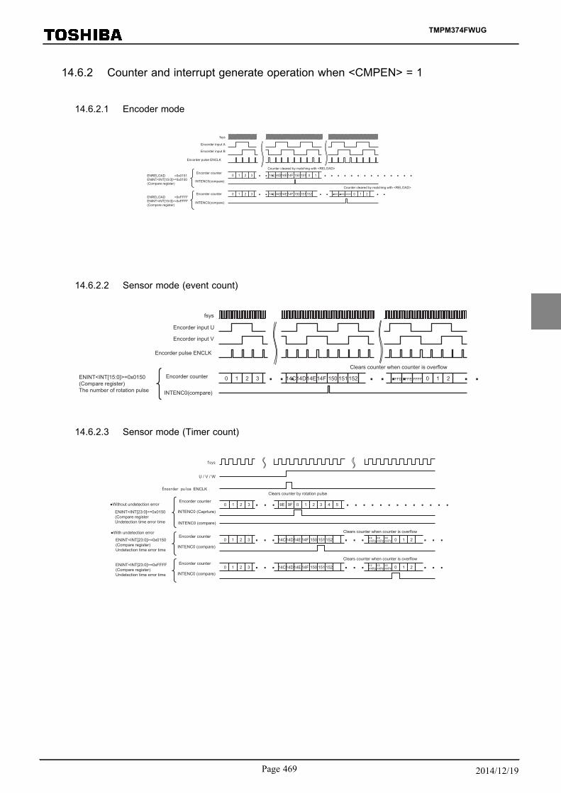
14.6.2 Counter and interrupt generate operation when <CMPEN> = 1
14.6.2.1 Encoder mode
INTENC0(compare)
0 1 2 3 14C14D14E14F 150 151 152 FFFD FFFE FFFF 0 1 2ENRELOAD =0xFFFFENINT<INT[15:0]>=0xFFFF(Compsre register)
0 1 2 3 14C14D14E14F 150 151 0
Counter cleared by matching with <RELOAD>
Counter cleared by matching with <RELOAD>
1
INTENC0(compare)
Encorder counter
Encorder counter
ENRELOAD =0x0151ENINT<INT[15:0]>=0x0150(Compare register)
Encorder pulse ENCLK
Encorder input A
Encorder input B
fsys
14.6.2.2 Sensor mode (event count)
Encorder pulse ENCLK
Encorder input U
Encorder input V
fsys
INTENC0(compare)
Encorder counter 0 1 2 3 14C14D14E14F 150 151 152 FFFD FFFE FFFF 0 1 2ENINT<INT[15:0]>=0x0150(Compare register)The number of rotation pulse
Clears counter when counter is overflow
14.6.2.3 Sensor mode (Timer count)
0 1 2 3 14C14D14E14F 150 151 152
0 1 2 3 9E 9F 0 1 2 3 4 5
FF_FFFD
FF_FFFE
FF_FFFF 0 1 2
0 1 2 3 14C14D14E14F 150 151 152 FF_FFFD
FF_FFFE
FF_FFFF 0 1 2
ENCLK
U / V / W
ENINT<INT[23:0]>=0x0150(Compare registerUndetection time error time
●Without undetection error
ENINT<INT[23:0]>=0xFFFF(Compare register)Undetection time error time
ENINT<INT[23:0]>=0x0150(Compare register)Undetection time error time
●With undetection error
INTENC0 (compare)
Encorder counter
INTENC0 (compare)
Encorder counter
INTENC0 (Caprture)
Encorder counter
INTENC0 (compare)
Clears counter by rotation pulse
Clears counter when counter is overflow
Clears counter when counter is overflow
TMPM374FWUG
Page 469 2014/12/19
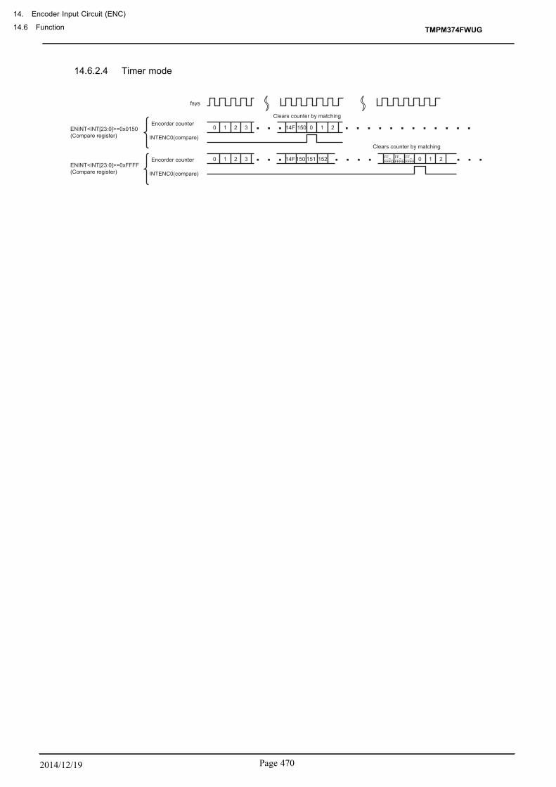
14.6.2.4 Timer mode
INTENC0(compare)
Encorder counter 0 1 2 3 14F 150 151 152 FF_FFFD
FF_FFFE
FF_FFFF 0 1 2
ENINT<INT[23:0]>=0xFFFF(Compare register)
0 1 2 3
Clears counter by matching
Clears counter by matching
14F 150 1 2
INTENC0(compare)
Encorder counterENINT<INT[23:0]>=0x0150(Compare register)
fsys
0
TMPM374FWUG
14. Encoder Input Circuit (ENC)
14.6 Function
Page 4702014/12/19
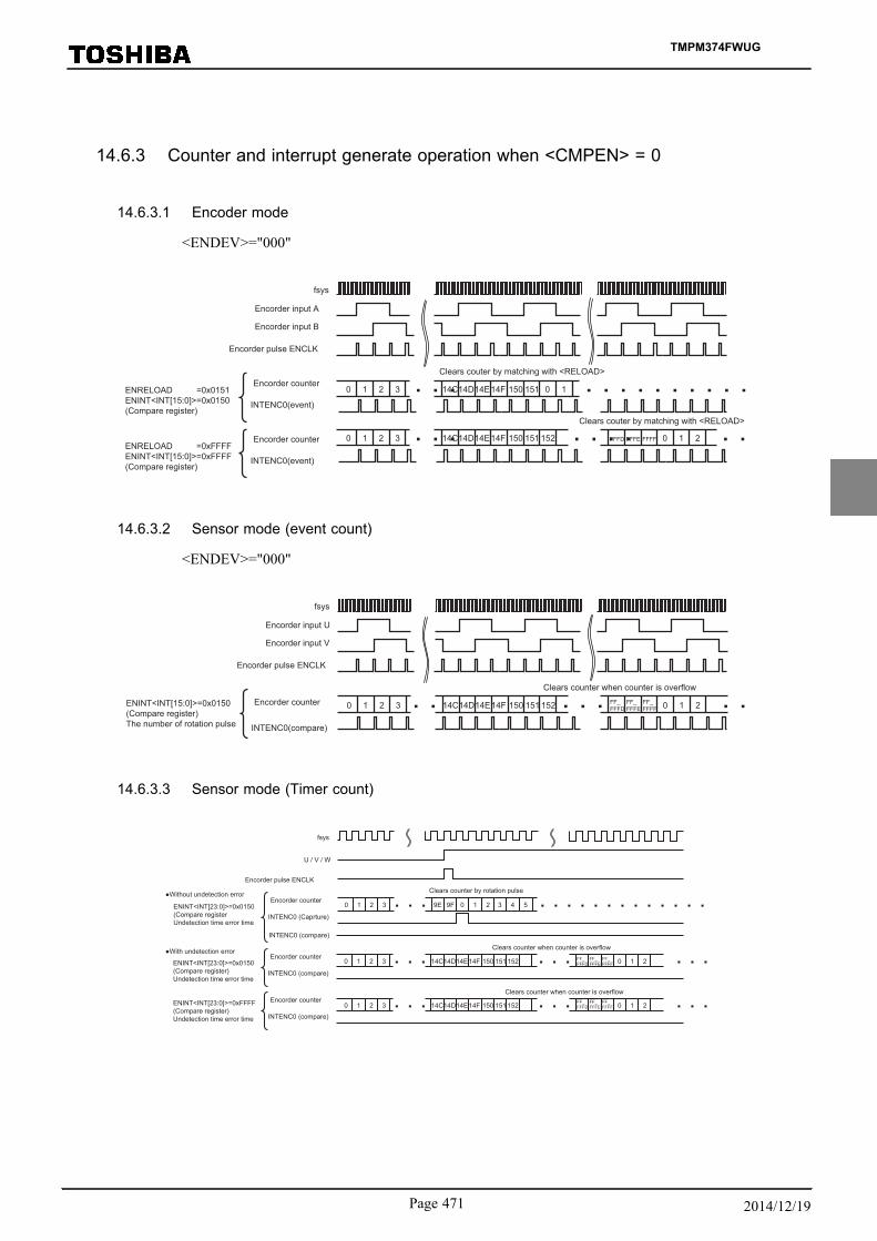
14.6.3 Counter and interrupt generate operation when <CMPEN> = 0
14.6.3.1 Encoder mode
<ENDEV>="000"
INTENC0(event)
Encorder counter 0 1 2 3 14C14D14E14F 150 151 152 FFFD FFFE FFFF 0 1 2ENRELOAD =0xFFFFENINT<INT[15:0]>=0xFFFF(Compare register)
0 1 2 3 14C14D14E14F 150 151 0
Clears couter by matching with <RELOAD>
Clears couter by matching with <RELOAD>
1
INTENC0(event)
Encorder counterENRELOAD =0x0151ENINT<INT[15:0]>=0x0150(Compare register)
Encorder pulse ENCLK
Encorder input A
Encorder input B
fsys
14.6.3.2 Sensor mode (event count)
<ENDEV>="000"
Encorder pulse ENCLK
Encorder input U
Encorder input V
fsys
INTENC0(compare)
Encorder counter 0 1 2 3 14C14D14E14F 150 151 152 FF_FFFD
FF_FFFE
FF_FFFF 0 1 2ENINT<INT[15:0]>=0x0150
(Compare register)The number of rotation pulse
Clears counter when counter is overflow
14.6.3.3 Sensor mode (Timer count)
INTENC0 (compare)
Encorder counterENINT<INT[23:0]>=0xFFFF(Compare register)Undetection time error time
0 1 2 3
INTENC0 (compare)
Encorder counterENINT<INT[23:0]>=0x0150(Compare register)Undetection time error time
14C14D14E14F 150 151 152
Clears counter by rotation pulse
0 1 2 3
INTENC0 (Caprture)
Encorder counterENINT<INT[23:0]>=0x0150(Compare registerUndetection time error time
9E 9F 0 1 2 3 4 5
Clears counter when counter is overflow
Clears counter when counter is overflow
INTENC0 (compare)
FF_FFFD
FF_FFFE
FF_FFFF 0 1 2
0 1 2 3 14C14D14E14F 150 151 152FF_FFFD
FF_FFFE
FF_FFFF 0 1 2
fsys
Encorder pulse ENCLK
U / V / W
●With undetection error
●Without undetection error
TMPM374FWUG
Page 471 2014/12/19

14.6.3.4 Timer mode
INTENC0(compare)
Encorder counter 0 1 2 3 14F 150 151 152 FFFD FFFE FFFF 0 1 2ENINT<INT[23:0]>=0xFFFF(Compare register)
0 1 2 3
Clears counter by matching
Clears counter by matching
14F 150 1 2
INTENC0(compare)
Encorder counterENINT<INT[23:0]>=0x0150(Compare register)
fsys
0
TMPM374FWUG
14. Encoder Input Circuit (ENC)
14.6 Function
Page 4722014/12/19
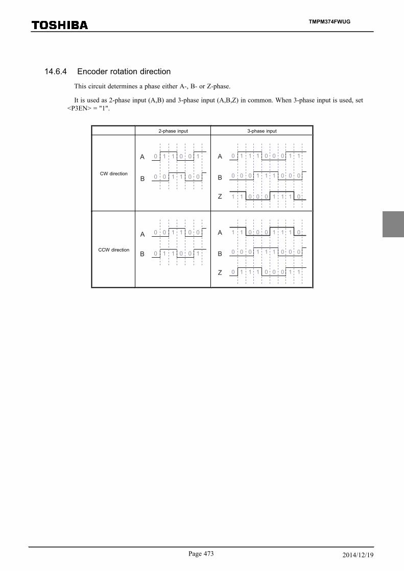
14.6.4 Encoder rotation direction
This circuit determines a phase either A-, B- or Z-phase.
It is used as 2-phase input (A,B) and 3-phase input (A,B,Z) in common. When 3-phase input is used, set<P3EN> = "1".
2-phase input 3-phase input
CW direction
0 1A
B
001 1
0 1 010 0
0 1A
B
011 0
0 0 110 1
0 1 1
0 0 0
1 0 001 1 1 1 0Z
CCW direction0 1B
A
001 1
0 1 010 0 A
B 0 0 110 1
0 1 011 0 0 1 1
0 0 0
1 0 001 1 1 1 0
Z
TMPM374FWUG
Page 473 2014/12/19

14.6.5 Counter Circuit
The counter circuit has a 24-bit up/down counter.
14.6.5.1 Operation Description
Depending on the operation modes, counting, clearing and reloading operation are controlled as descri-bed in Table 14-2.
Table 14-2 Counter control
Mode<MODE[1:0]>
<ZEN> <P3EN> Inputpin Count Opera-
tionCounter clear condi-
tionCounter reload
condition
Operationalrange of coun-
ter(Reload value)
Encoder mode00
0
0
A,B
Encoderpulse
(ENCLK)
UP[1]<ENCLR> = 1 WR[2] Matches with <RE-LOAD>
-
0x0000 to <RE-LOAD>
DOWN [1]<ENCLR> = 1 WR [1] Matches with0x0000
1 A,B,ZUP
[1]<ENCLR> = 1 WR[2] Matches with <RE-LOAD>[3] Z-trigger
-
DOWN [1]<ENCLR> = 1 WR [1] Matches with0x0000
Sensor mode(event count)
010
0 U,VUP
[1]<ENCLR> = 1 WR[2] Matches with0xFFFF
-
0x0000 to0xFFFF
DOWN [1]<ENCLR> = 1 WR [1] Matches with0x0000
1 U,V,WUP
[1]<ENCLR> = 1 WR[2] Matches with0xFFFF
-
DOWN [1]<ENCLR> = 1 WR [1] Matches with0x0000
Sensor mode(Timer count)
100
0 U,V
fsys
UP[1]<ENCLR> = 1 WR[2] Matches with0xFFFFFF
-0x000000 to0xFFFFFF
1 U,V,W UP[3] Encoder pulse(ENCLK)
-
Timer mode11
0
×
- UP
[1]<ENCLR> = 1 WR[2] Matches with0xFFFFFF[3] Matches with<EN1INT>
-
0x000000 to0xFFFFFF
1 Z UP
[1]<ENCLR> = 1 WR[2] Matches with0xFFFFFF[3] Matches with<EN1INT>[4] Z-trigger
-
Note:The counter value is not cleared by writing "0" to <ENRUN>. If <ENRUN> = "1" is set again, the coun-ter restarts from the counter value which has stopped. If clear the counter value, write "1" to<ENCLR> to execute software clear.
TMPM374FWUG
14. Encoder Input Circuit (ENC)
14.6 Function
Page 4742014/12/19

14.6.6 Interrupt
The interrupt consists of four interrupts including Event (divide pulse and capture), Abnormal detectingtime, Timer compare and Capture interrupts.
14.6.6.1 Operational Description
When <INTEN> = "1" is set, interrupts occurs by counter value and encoder pulses.
Interrupt factor setting consists of six kinds setting with operation modes and the setting of <CMPEN>and <ZEN>.Table 14-3 shows interrupt factors.
Table 14-3 Interrupt factors
Interrupt factor Description Mode Interrupt output Status flag
1 Event count interrupt
When <CMPEN> = 1, the encodercounter counts events (encoder pul-ses). When it has reached to the val-ue programmed in <EN1INT>, an inter-rupt occurs.
Encoder modeand
Sensor mode(event count)
<INTEN> = 1and
<CMPEN> = 1<CMP>
2Event interrupt(divide pulse)
An interrupt occurs on each dividedclock pulse (1 to 128 divide), which isderived by dividing the encoder pulseby a factor programmed in <ENDEV>.
<INTEN> = 1 Not available
3Event interrupt(capture interrupt)
An interrupt occurs to indicate that anevent (encoder pulse) has occurred,causing the counter value to be cap-tured on the rotation pulse timing.
Sensor mode(Timer count)
<INTEN> = 1 Not available
4 Abnormal detection time er-ror interrupt
When <CMPEN> = 1, the ENC usesa counter that counts up with fsys andis cleared by an event (encoderpulse). If no event occurs for a periodof time programmed in <EN1INT>, aninterrupt occurs.
<INTEN> = 1and
<CMPEN> = 1<CMP>
5 Timer compare interruptWhen <CMPEN> = 1, an interrupt oc-curs when the timer has reached tothe value programmed in <EN1INT>.
Timer mode
<INTEN> = 1and
<CMPEN> = 1<CMP>
6 Capture interruptAn interrupt occurs when the countervalue has been captured on an exter-nal trigger (Z input).
<INTEN> = 1 Not available
In Sensor Timer Count mode and Timer mode, the value of the encoder counter can be captured intothe EN1CNT register.
The captured counter value can be read out of the EN1CNT register.
In Sensor Timer Count mode, the value of the encoder counter is captured into the EN1CNT registerupon occurrence of an event (encoder pulse). The counter value can also be captured by writing a 1 to<SFTCAP> by software.
In Timer mode, the counter value can be captured by writing a 1 to <SFTCAP> by software. If<ZEN> is set to 1, the counter value can also be captured by an edge of the Z signal input selected accord-ing to <ZESEL> by external trigger.
TMPM374FWUG
Page 475 2014/12/19

TMPM374FWUG
14. Encoder Input Circuit (ENC)
14.6 Function
Page 4762014/12/19

15. Power-on-Reset Circuit (POR)
The power-on-reset circuit (POR) generates a power-on reset signal when power-on.
When the supply voltage is lower than the detection voltage of the power-on reset circuit, a power-on reset sig-nal is generated.
Power supply voltage means DVDD5 and RVDD5.
15.1 StructurePower-on-reset circuit consists of the reference voltage generation circuit, comparators, the VLTD reset circuit
and the power-on counter.
This circuit compares a voltage divided by the ladder resistor with a reference voltage generated in the refer-ence voltage generation circuit in the comparator.
Power-on counter
Power-on detect signal
Power-on-reset signal-
+
Power supply voltage
Reference voltage
generation circuit
Figure 15-1 Power-on-reset circuit
15.2 FunctionAt power-on, a power-on detection signal generates while power supply voltage is lower than the releasing volt-
age. Power-on detection signal is released at the timing when DVDD5 and RVDD5 is over 3.0 ±0.2 V.
If the power-on detection signal is released and the reset detection signal is also released, the power-on counterstarts to operate. After waiting time (approximately 215/fosc2 s) has elapsed, the power-on reset signal is released.
During the power-on reset signal generation, the CPU and the peripheral functions are reset.
When a reset input is not used, supply voltage must be raised to the recommended operational voltage range un-til the power-on reset releasing. If power supply voltage does not reach to the recommended operational voltagerange during this period, TMPM374FWUG cannot operate properly.
TMPM374FWUG
Page 477 2014/12/19

0V
Reset detect signal”Low” active)
Internal 1.5V power suppy voltage
reset release voltage(VPORH)
Detect voltage (VPORL)
Power suppy voltageOpration voltage range
tPWUP
tDVDD
3.9V
Power-on-reset signal”Low” active)
Power-on counter
Power-on detect signal”Low” active)
Figure 15-2 Power-on-reset operation timing
Symbol Parameter Min. Typ. Max. Unit
tPWUP Power-on Counter - 215/fOSC2 - s
tDVDD Rising time of power line - - 3 ms
VPORH Power-on Reset releasing voltage 2.8 3 3.2 V
VPORL Power-on Reset detection voltage 2.6 2.8 3.0 V
tPORDT1 Power-on Reset release sesponse time 30 μS
Note:Since the power-on releasing voltage and the power-on reset detection voltage relatively change,the detec-tion voltage is never reversed.
Note:Due to the fluctuation of supply voltage, the power-on reset circuit may not operate properly. Users shouldgive due consideration based on the electrical characteristic in the device designing.
TMPM374FWUG
15. Power-on-Reset Circuit (POR)
15.2 Function
Page 4782014/12/19

16. Low Voltage Detection Circuit (VLTD)
The low voltage detection circuit generates a reset signal by detecting a decreasing voltage.
Power supply voltage means DVDD5 and RVDD5.
Note:Due to the fluctuation of supply voltage, the voltage detection circuit may not operate properly. Users shouldgive due consideration based on the electrical characteristic in the device designing.
16.1 StructureThe low voltage detection circuit consists of a reference voltage generation circuit, a detection voltage level selec-
tion circuit, a comparator and control registers.
The power supply voltage is divided by the ladder resistor and input to the detection voltage selection circuit.The detection voltage selection circuit selects a voltage according to the specified detection voltage (VDLVL),and the comparator compares it with the reference voltage. When the power supply voltage becomes lower thanthe detection voltage (VDLVL), a voltage detection reset signal is generated.
VDCR
VDLVL
VD
EN
Power supply voltage
VDLVL1
Voltage detection reset
Det
ectio
n vo
ltage
leve
l sel
ectio
n ci
rcui
t
Reference voltagegeneration circuit
Figure 16-1 Voltage Detection Circuit)
TMPM374FWUG
Page 479 2014/12/19

16.2 Registers
16.2.1 Register List
Base Address = 0x4004_0900
Register name Address(Base+)
Voltage detection control register VDCR 0x0000
16.2.2 VDCR (Voltage detection control register)
31 30 29 28 27 26 25 24
bit symbol − − − − − − − −
After reset 0 0 0 0 0 0 0 0
23 22 21 20 19 18 17 16
bit symbol − − − − − − − −
After reset 0 0 0 0 0 0 0 0
15 14 13 12 11 10 9 8
bit symbol − − − − − − - −
After reset 0 0 0 0 0 0 0 0
7 6 5 4 3 2 1 0
bit symbol − − − − − VDLVL VDEN
After reset 0 0 0 0 0 0 0 0
Bit Bit Symbol Type Function
31-3 − R Read as "0".
2-1 VDLVL[1:0] R/W Selection for detection voltage00: Reserved01: 4.1 ± 0.2V10: 4.4 ± 0.2V11: 4.6 ± 0.2V
0 VDEN R/W Low voltage detection operation
0: Disabled1: Enabled
Note:VDCR is initialized by a power-on reset or an external reset input.
TMPM374FWUG
16. Low Voltage Detection Circuit (VLTD)
16.2 Registers
Page 4802014/12/19

16.3 Operation Description
16.3.1 Control
The voltage detection circuit is controlled by voltage detection control registers.
16.3.2 Function
The detection voltage can be selected by VDCR<VDLVL[1:0]>. Enabling/disabling the voltage detectioncan be programmed by VDCR<VDEN>. After the voltage detection operation is enabled, When the power sup-ply voltage becomes lower than the detection voltage <VDLVL[1:0]>, a voltage detection reset signal is gen-erated.
16.3.2.1 Enabling/disabling the voltage detection operation
Setting VDCR<VDEN> to "1" enables the voltage detection operation. Setting it to "0" disables the op-eration. VDCR<VDEN> is cleared to "0" immediately after a power-on reset or a reset by an external re-set input is released.
Note:When the supply voltage (DVDD5B) is lower than the detection voltage VDCR<VDLVL[1:0]>, set-ting VDCR<VDEN> to "1" generates reset signal at the time.
16.3.2.2 Selecting the detection voltage level
Select a detection voltage at VDCR<VDLVL[1:0]>.
Power voltage
VLTDdetection voltage
Power-on resetsignal
PORdetection voltage
Voltage detectionenable
Voltage detectionreset signal
tVDPW
tVDEN
tVDDT1 tVDDT2
Software Software
tVDDT1
Figure 16-2 Voltage Detection Timing
Symbol Parameter Min. Typ. Max. Unit
tVDEN Setup time after enabling voltage detection - 40 -
μstVDDT1 Voltage detection response time - 40 -
tVDDT2 Voltage detection releasing time‘ - 40 -
tVDPW Voltage detection minimum pulse width 45 - -
TMPM374FWUG
Page 481 2014/12/19

TMPM374FWUG
16. Low Voltage Detection Circuit (VLTD)
16.3 Operation Description
Page 4822014/12/19

17. Ocsillation Frequency Detector (OFD)
The oscillation frequency detector generates a reset for I/O if the oscillation of external high frequency forCPU clock exceeds the detection frequency range.
The oscillation frequency detection is controlled by OFDCR1, OFDCR2 registers and the detection frequencyrange is specified by OFDMNPLLOFF/OFDMNPLLON/OFDMXPLLOFF/OFDMXPLLON which are the detec-tion frequency setting registers. The lower detection frequency is specified by OFDMNPLLOFF/OFDMNPLLONregisters and the higher detection frequency is specified by OFDMXPLLOFF/OFDMXPLLON registers.
When the oscillation frequency detection is enabled, writing to OFDMNPLLOFF/OFDMNPLLON/OFDMXPLL-OFF/OFDMXPLLON registers is disabled. Therefore, the setting the detection frequency to these registers shouldbe done when the oscillation frequency detection is disabled. And writing to OFDCR2/OFDMNPLLOFF/OFDMNPLLON/OFDMXPLLOFF/OFDMXPLLON registers is controlled by OFDCR1 register. To writeOFDCR2/OFDMNPLLOFF/OFDMNPLLON/OFDMXPLLOFF/OFDMXPLLON registers, the write enable code"0xF9" should be set to OFDCR1 beforehand. To enable the oscillation frequency detector, set "0xE4" toOFDCR2 after setting "0xF9" to OFDCR1. Since the oscillation frequency detection is disabled after an external re-set input, power on reset or VLTD reset, write "0xF9" to OFDCR1 and write "0xE4" to OFDCR2 register to ena-ble its function.
When the TMPM374FWUG detects the out of frequency by lower and higher detection frequency setting regis-ters, all I/Os become high impedance by reset. In case of PLLOFF, OFDMNPLLOFF and OFDMXPLLOFF regis-ters are valid for detection and the setting value of OFDMNPLLON/OFDMXPLLON registers are ignored. Incase of PLLON, OFDMNPLLON and OFDMXPLLON registers are valid for detection and the setting value ofOFDMNPLLOFF/OFDMXPLLOFF registers are ignored. By the oscillation frequency detection reset, all I/Os ex-cept power supply pins, RESET pin and MODE pin become high impedance and the CPU is also initialized. Asthe CG registers are initialized, so the PLL operation of the system clock is disabled and the clock operation is re-started after switching an oscillator to on chip oscillation (fosc2).
Since all registers for oscillation frequency detector (OFDCR1/OFDCR2/OFDMNPLLOFF/OFDMNPLLON/OFDMXPLLOFF/OFDMXPLLON) are not initialized by the reset generated from oscillation frequency detector.
And so when the oscillation frequency detection reset is generated, the system clock is switched to on chip oscil-lation and the reset sequence is executed just as the oscillation frequency detection is enabled.
Note:It is not guaranteed that OFD can detect all defects at any time, and it is not a circuit to measure error frequen-cy.
Note:The oscillation frequency detection reset is available only in NORMAL and IDLE modes. In STOP mode, theoscillation frequency detection reset is disabled automatically.
Note:When the PLL is controlled (enabled or disabled) by the CGPLLSEL register or when the system clock ischanged (fosc1 or fosc2) by the <OSCSEL> of CGOSCCR register, the OFD must be disabled beforehand.If OFD reset is generated with PLL-ON, the detection frequency setting registers (OFDMNPLLON/OFDMXPL-LON) are automatically switched over to OFDMNPLLOFF/OFDMXPLLOFF.
TMPM374FWUG
Page 483 2014/12/19

17.1 Block diagram
Reference clock
Target detection clock
Oscillation Frequency Detection Circuit
OFD
Internal data bus
OFD reset
OFDCR1
OFDCR2
OFDMNPLLOFF
OFDMXPLLOFF
X1X2 fosc2
OFDMNPLLON
OFDMXPLLON
CGOSCCR<OSCSEL>
Switch intend detection clock
fosc1
PLLCGOSCCR<PLLON>
CGPLLSEL<PLLSEL>
fc
Figure 17-1 Ocsillation Frequency Detector Block diagram
TMPM374FWUG
17. Ocsillation Frequency Detector (OFD)
17.1 Block diagram
Page 4842014/12/19

17.2 Registers
17.2.1 Register List
Base Address = 0x4004_0800
Register name Address(Base+)
Oscillation frequency detection control register 1 OFDCR1 0x0000
Oscillation frequency detection control register 2 OFDCR2 0x0004
Lower detection frequency setting register (PLL OFF) OFDMNPLLOFF 0x0008
Lower detection frequency setting register (PLL ON) OFDMNPLLON 0x000C
Higher detection frequency setting register (PLL OFF) OFDMXPLLOFF 0x0010
Higher detection frequency setting register (PLL ON) OFDMXPLLON 0x0014
Note:Access to the "Reserved" area is prohibited.
TMPM374FWUG
Page 485 2014/12/19

17.2.1.1 OFDCR1 (Oscillation frequency detection control register)
31 30 29 28 27 26 25 24
bit symbol - - - - - - - -
After reset 0 0 0 0 0 0 0 0
23 22 21 20 19 18 17 16
bit symbol - - - - - - - -
After reset 0 0 0 0 0 0 0 0
15 14 13 12 11 10 9 8
bit symbol - - - - - - - -
After reset 0 0 0 0 0 0 0 0
7 6 5 4 3 2 1 0
bit symbol OFDWEN
After reset 0 0 0 0 0 1 1 0
Bit Bit Symbol Type Description
31-8 − R Read as 0.
7-0 OFDWEN[7:0] R/W Controls register write0x06: Disable0xF9: EnableSetting 0xF9 enables to write registers except OFDCR1.When writing a value except 0x06 or 0xF9, 0x06 is written.If writing register is disabled, reading from each register is enabled.
Note:OFDCR1 is initialized by the RESET pin, power on reset or VLTD reset.
TMPM374FWUG
17. Ocsillation Frequency Detector (OFD)
17.2 Registers
Page 4862014/12/19

17.2.1.2 OFDCR2 (Oscillation frequency detection control register 2)
31 30 29 28 27 26 25 24
bit symbol - - - - - - - -
After reset 0 0 0 0 0 0 0 0
23 22 21 20 19 18 17 16
bit symbol - - - - - - - -
After reset 0 0 0 0 0 0 0 0
15 14 13 12 11 10 9 8
bit symbol - - - - - - - -
After reset 0 0 0 0 0 0 0 0
7 6 5 4 3 2 1 0
bit symbol OFDEN
After reset 0 0 0 0 0 0 0 0
Bit Bit Symbol Type Description
31-8 − R Read as 0.
7-0 OFDEN[7:0] R/W Controls frequency detecting.0x00: Disable0xE4: EnableWriting a value except 0x00 or 0xE4 is invalid and a value will not be changed.
Note:OFDCR2 is initialized by the RESET pin, power on reset or VLTD reset.
TMPM374FWUG
Page 487 2014/12/19
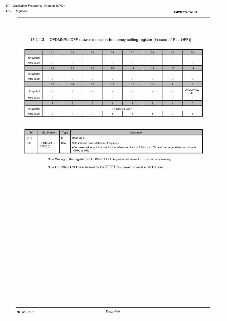
17.2.1.3 OFDMNPLLOFF (Lower detection frequency setting register (In case of PLL OFF))
31 30 29 28 27 26 25 24
bit symbol - - - - - - - -
After reset 0 0 0 0 0 0 0 0
23 22 21 20 19 18 17 16
bit symbol - - - - - - - -
After reset 0 0 0 0 0 0 0 0
15 14 13 12 11 10 9 8
bit symbol - - - - - - - OFDMNPLL-OFF
After reset 0 0 0 0 0 0 0 0
7 6 5 4 3 2 1 0
bit symbol OFDMNPLLOFF
After reset 0 0 0 1 1 1 0 1
Bit Bit Symbol Type Description
31-9 − R Read as 0.
8-0 OFDMNPLL-OFF[8:0]
R/W Sets internal lower detection frequency.After reset value which is set for the reference clock is 9.5MHz ± 10% and the target detection clock is10MHz ± 10%.
Note:Writing to the register of OFDMNPLLOFF is protected while OFD circuit is operating.
Note:OFDMNPLLOFF is initialized by the RESET pin, power on reset or VLTD reset.
TMPM374FWUG
17. Ocsillation Frequency Detector (OFD)
17.2 Registers
Page 4882014/12/19
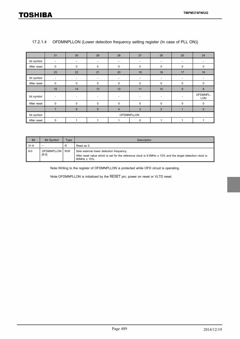
17.2.1.4 OFDMNPLLON (Lower detection frequency setting register (In case of PLL ON))
31 30 29 28 27 26 25 24
bit symbol - - - - - - - -
After reset 0 0 0 0 0 0 0 0
23 22 21 20 19 18 17 16
bit symbol - - - - - - - -
After reset 0 0 0 0 0 0 0 0
15 14 13 12 11 10 9 8
bit symbol - - - - - - - OFDMNPL-LON
After reset 0 0 0 0 0 0 0 0
7 6 5 4 3 2 1 0
bit symbol OFDMNPLLON
After reset 0 1 1 1 0 1 1 1
Bit Bit Symbol Type Description
31-9 − R Read as 0.
8-0 OFDMNPLLON[8:0]
R/W Sets external lower detection frequency.After reset value which is set for the reference clock is 9.5MHz ± 10% and the target detection clock is80MHz ± 10%.
Note:Writing to the register of OFDMNPLLON is protected while OFD circuit is operating.
Note:OFDMNPLLON is initialized by the RESET pin, power on reset or VLTD reset.
TMPM374FWUG
Page 489 2014/12/19

17.2.1.5 OFDMXPLLOFF (Higher detection frequency setting register (In case of PLL OFF))
31 30 29 28 27 26 25 24
bit symbol - - - - - - - -
After reset 0 0 0 0 0 0 0 0
23 22 21 20 19 18 17 16
bit symbol - - - - - - - -
After reset 0 0 0 0 0 0 0 0
15 14 13 12 11 10 9 8
bit symbol - - - - - - - OFDMXPLL-OFF
After reset 0 0 0 0 0 0 0 0
7 6 5 4 3 2 1 0
bit symbol OFDMXPLLOFF
After reset 0 0 1 0 0 1 0 1
Bit Bit Symbol Type Description
31-9 − R Read as 0.
8-0 OFDMXPLL-OFF[8:0]
R/W Sets internal higher detection frequency.After reset value which is set for the reference clock is 9.5MHz ± 10% and the target detection clock is10MHz ± 10%.
Note:Writing to the register of OFDMXPLLOFF is protected while OFD circuit is operating.
Note:OFDMXPLLOFF is initialized by the RESET pin, power on reset or VLTD reset.
TMPM374FWUG
17. Ocsillation Frequency Detector (OFD)
17.2 Registers
Page 4902014/12/19

17.2.1.6 OFDMXPLLON (Higher detection frequency setting register (In case of PLL ON))
31 30 29 28 27 26 25 24
bit symbol - - - - - - - -
After reset 0 0 0 0 0 0 0 0
23 22 21 20 19 18 17 16
bit symbol - - - - - - - -
After reset 0 0 0 0 0 0 0 0
15 14 13 12 11 10 9 8
bit symbol - - - - - - - OFDMXPL-LON
After reset 0 0 0 0 0 0 0 0
7 6 5 4 3 2 1 0
bit symbol OFDMXPLLON
After reset 1 0 0 0 1 1 1 1
Bit Bit Symbol Type Description
31-9 − R Read as 0.
8-0 OFDMXPLLON[8:0]
R/W Sets external higher detection frequency.After reset value which is set for the reference clock is 9.5MHz ± 10% and the target detection clock is88MHz.
Note:Writing to the register of OFDMXPLLON is protected while OFD circuit is operating.
Note:OFDMXPLLON is initialized by the RESET pin, power on reset or VLTD reset.
TMPM374FWUG
Page 491 2014/12/19
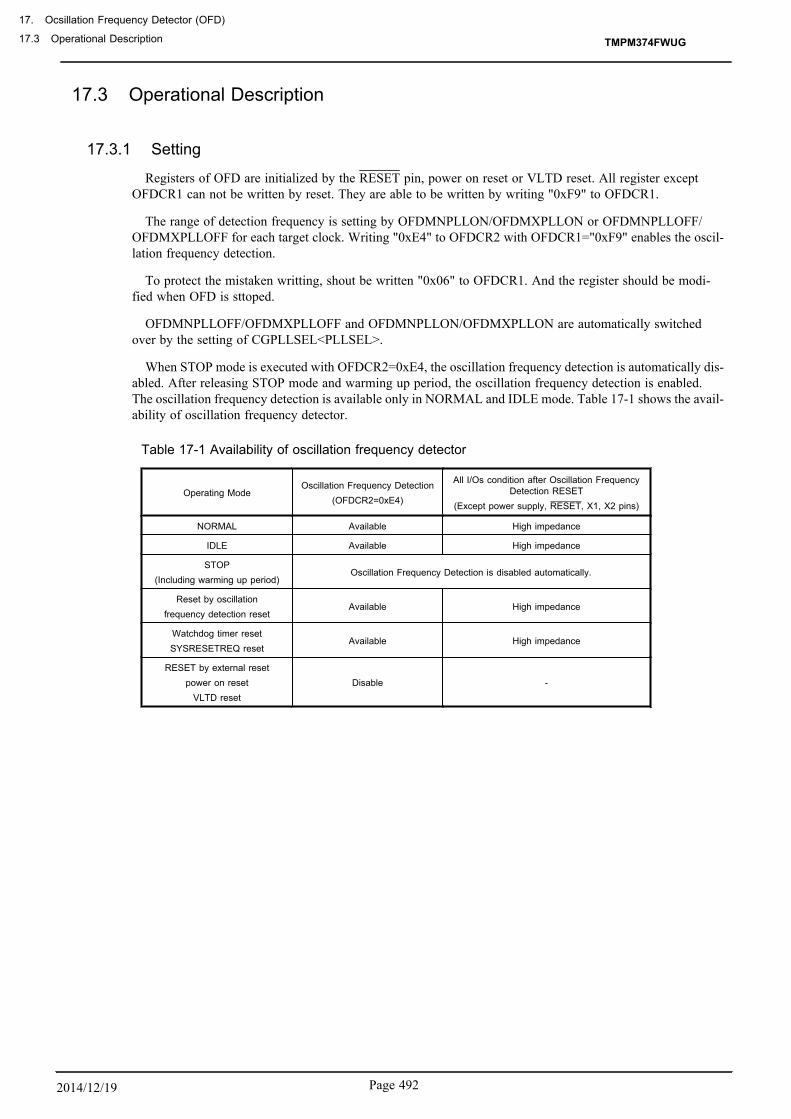
17.3 Operational Description
17.3.1 Setting
Registers of OFD are initialized by the RESET pin, power on reset or VLTD reset. All register exceptOFDCR1 can not be written by reset. They are able to be written by writing "0xF9" to OFDCR1.
The range of detection frequency is setting by OFDMNPLLON/OFDMXPLLON or OFDMNPLLOFF/OFDMXPLLOFF for each target clock. Writing "0xE4" to OFDCR2 with OFDCR1="0xF9" enables the oscil-lation frequency detection.
To protect the mistaken writting, shout be written "0x06" to OFDCR1. And the register should be modi-fied when OFD is sttoped.
OFDMNPLLOFF/OFDMXPLLOFF and OFDMNPLLON/OFDMXPLLON are automatically switchedover by the setting of CGPLLSEL<PLLSEL>.
When STOP mode is executed with OFDCR2=0xE4, the oscillation frequency detection is automatically dis-abled. After releasing STOP mode and warming up period, the oscillation frequency detection is enabled.The oscillation frequency detection is available only in NORMAL and IDLE mode. Table 17-1 shows the avail-ability of oscillation frequency detector.
Table 17-1 Availability of oscillation frequency detector
Operating ModeOscillation Frequency Detection
(OFDCR2=0xE4)
All I/Os condition after Oscillation FrequencyDetection RESET
(Except power supply, RESET, X1, X2 pins)
NORMAL Available High impedance
IDLE Available High impedance
STOP(Including warming up period)
Oscillation Frequency Detection is disabled automatically.
Reset by oscillationfrequency detection reset
Available High impedance
Watchdog timer resetSYSRESETREQ reset
Available High impedance
RESET by external resetpower on reset
VLTD resetDisable -
TMPM374FWUG
17. Ocsillation Frequency Detector (OFD)
17.3 Operational Description
Page 4922014/12/19

17.3.2 Operation
From the operation start-up to detection start-up, time length as two cycle of detecting clock is needed.And the Detecting cycle is 128/reference clock frequency.
When generating reset is enabled, OFD generates reset if the target clock frequency exceeds the frequencylimit set by OFDMNPLLON/OFDMXPLLON and OFDMNPLLOFF/OFDMXPLLOFF. From detection of ab-normal to reset generation, time length as one cycle of detecting clock is needed. The reset generated byOFD does not make itself and OFD continues detected operation.
Therefore, fosc is initialized to fosc2 and the target clock(fc) changes to fosc2 and detected operation is con-tinued in PLL OFF.
Note:There are several factors of reset. Clock generator register CGRSTFLG can confirm the factors. For de-tails of CGRSTFLG see chapter "exception."
Note:The target clock is set without 10MHz into OFDMNPLLOFF and OFDMXPLLOFF. (eg, setting to8MHz value to these registers) And when the target clock frequency is fosc1 and the reset gener-ated by OFD, the reset might be generated continuously due to as abnormal detection until OFD de-tects correctly.
Power supply
On chip oscillator(fosc2)
External frequency(fosc1)
POR(Power on reset)
OFD reset(Oscillation frequency detection reset)
OFD function Disable
Reference Clock
RESET pin
OFD detectedTarget detection Clock
Reference Clock
External frequency: ON& Warm-up
Switch to external frequency& OFD function enable
Enable
External frequency: ON& Warm-up
Target detection &Reference Clock
Clear reset flag<OFDRSTF>& OFD function disable
Disable Enable
Switch to external frequency& OFD function enable
Note: The target clock is set without 10MHz into OFDMNPLLOFF and OFDMXPLLOFF. (eg, setting to 8MHz value to these registers) And when the target clock frequency is fosc1 and the reset generated by OFD, the reset might be generated continuously due to as abnormal detection until OFD detects correctly.
Target detection Clock
As fosc2 function is normally, the OFDreset is cleared. (Note)
Figure 17-2 Example of oscillation frequency detection operation
TMPM374FWUG
Page 493 2014/12/19

17.3.3 Detection Frequency
The detection frequency have a detection frequency range and an undetectable frequency range because ofoscillation accuracy. Therefore, it is undefined whether to be detected between detection frequency rangeand undetectable it.
The upper and lower limit of detecting frequency are calcurated by the maxmum error of a target clockand a reference clock.
By the way of rounding the calcurated result when OFDMNPLLON/OFDMNPLLOFF and OFDMXPLLON/OFDMXPLLOFF are decided, the upper and lower limit of detecting and undetecting range shown as fol-lows. The way of rouding is selected depending on the uneveness of the detected clock.
・ In case of rounding up OFDMXPLLON/OFDMXPLLOFF and rouding down OFDMNPLLON/OFDMNPLLOFF
The target clock is higher than the upper limit of undetecting ragne and lower than the lower lim-it of undetecting range.
・ In case of rounding down OFDMXPLLON/OFDMXPLLOFF and rouding down OFDMNPLLON/OFDMNPLLOFF
The target clock is lower than the upper limit of undetecting ragne and higher than the lower lim-it of undetecting range.
How to calculate the setup value of OFDMXPLLOFF/OFDMNPLLOFF is shown below when the targetclock error is ±10% (undetecting range) and the reference clock error is ± 10%. In this example, OFDMXPLL-OFF is rounded up and OFDMNPLLOFF is rounded down.(From "a" to "h" corresponds to "Figure 17-3 Exam-ple of detection frequency range (in case of 10MHz)" )
target clock 10MHz ± 10%Max.11.0MHz -------- c
Min. 9.0MHz -------- b
reference clock 9.5MHz ± 10%Max.10.45MHz -------- f
Min. 8.55MHz -------- e
OFDMXPLLOFF = c ÷ e × 32 = 41.16... = 42 (Rounding up to nearest decimal) = 0x2A
OFDMNPLLOFF = b ÷ f × 32 = 27.55... = 27 (Rounding down to nearest decimal) = 0x1B
At this time, the detecting range is calculated shown below.
a = e × OFDMNPLLOFF ÷ 32 = 7.21
d = f × OFDMXPLLOFF ÷ 32 = 13.71
And the undetecting range is calculated shown below.
g = e × OFDMXPLLOFF ÷ 32 = 11.22
h = f × OFDMNPLLOFF ÷ 32 = 8.81
Setting "0x2A" to the register OFDMXPLLOFF and "0x1B" to the register OFDMNPLLOFF, when the tar-get clock of higher than 13.71MHz or lower than 7.21MHz is detected, the oscillation frequency detector out-puts a reset signal. And when the target clock of higher than 8.81MHz and lower than 11.22MHz is detected,the oscillation frequency detector does not output a reset signal.
Figure 17-3 shows the detection or undetectable and detectable frequency range.
TMPM374FWUG
17. Ocsillation Frequency Detector (OFD)
17.3 Operational Description
Page 4942014/12/19

Subharmonic(10MHz + 10%) ÷ 2, 3 ...
Detection range
Undetectable range
fOSC1 [MHz]
Harmonic(10MHz - 10%) * 2, 3 ...
a h
b c
10 g d
Figure 17-3 Example of detection frequency range (in case of 10MHz)
17.3.4 Available Operation Mode
The oscillation frequency detection is available only external oscillation frequency in NORMAL andIDLE mode. Before shifting to another mode or using on chip oscillation frequency, disable the oscillation fre-quency detection.
17.3.5 Example of Operational Procedure
The example of operational procedure is shown below.
After reset, confirms various reset factor by CGRSTFLG. If the reset factor is not by the oscillation frequen-cy detect, enable external oscillation, set register to use OFD and enable operation.
Error operation
no
Reset
Enable external oscillation setting
CGRSTFLG<OFDRSTF>=”0”
yes
OFD setting(OFDMNPLLON/OFF,OFDMXPLLON/OFF)
Enable write registerOFDCR1=0xF9)
Enable OFD operation(OFDCR2=0xE4)
Disable write registerOFDCR1=0x06)
Enable external oscillation<OSCSEL>=”1”)
Figure 17-4 Example of operational procedure
TMPM374FWUG
Page 495 2014/12/19

TMPM374FWUG
17. Ocsillation Frequency Detector (OFD)
17.3 Operational Description
Page 4962014/12/19

18. Watchdog Timer(WDT)
The watchdog timer (WDT) is for detecting malfunctions (runaways) of the CPU caused by noises or other distur-bances and remedying them to return the CPU to normal operation.
If the watchdog timer detects a runaway, it generates a INTWDT interrupt or reset.
Note:INTWDT interrupt is a factor of the non-maskable interrupts (NMI).
Also, the watchdog timer notifies of the detecting malfunction to the external peripheral devices from the watch-dog timer pin (WDTOUT) by outputting "Low".
Note:This product does not have the watchdog timer out pin (WDTOUT).
18.1 ConfigurationFigure 18-1shows the block diagram of the watchdog timer.
WDMOD<RESCR>
To internal reset
RESET pin
Watchdog timer out control
WDTOUT
Q
R S
Selector
Binary counter
215/fs
ys
217/fs
ys
219/fs
ys
221/fs
ys
223/fs
ys
225/fs
ys
WDMOD
fsys
WDMOD<WDTE>
Watch dog timer Control Register WDCR
Reset
Write“0xB1”
Write“0x4E”
Internal data bus
Internal reset
Watchdog timer interrupt INTWDT
Figure 18-1 Block Diagram of the Watchdog Timer
TMPM374FWUG
Page 497 2014/12/19
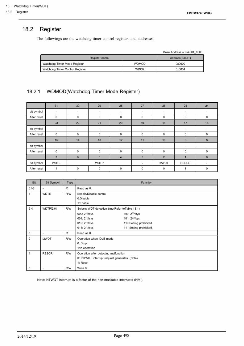
18.2 RegisterThe followings are the watchdog timer control registers and addresses.
Base Address = 0x4004_0000
Register name Address(Base+)
Watchdog Timer Mode Register WDMOD 0x0000
Watchdog Timer Control Register WDCR 0x0004
18.2.1 WDMOD(Watchdog Timer Mode Register)
31 30 29 28 27 26 25 24
bit symbol - - - - - - - -
After reset 0 0 0 0 0 0 0 0
23 22 21 20 19 18 17 16
bit symbol - - - - - - - -
After reset 0 0 0 0 0 0 0 0
15 14 13 12 11 10 9 8
bit symbol - - - - - - - -
After reset 0 0 0 0 0 0 0 0
7 6 5 4 3 2 1 0
bit symbol WDTE WDTP - I2WDT RESCR -
After reset 1 0 0 0 0 0 1 0
Bit Bit Symbol Type Function
31-8 − R Read as 0.
7 WDTE R/W Enable/Disable control0:Disable1:Enable
6-4 WDTP[2:0] R/W Selects WDT detection time(Refer toTable 18-1)
000: 215/fsys001: 217/fsys010: 219/fsys011: 221/fsys
100: 223/fsys101: 225/fsys110:Setting prohibited.111:Setting prohibited.
3 − R Read as 0.
2 I2WDT R/W Operation when IDLE mode0: Stop1:In operation
1 RESCR R/W Operation after detecting malfunction0: INTWDT interrupt request generates. (Note)1: Reset
0 − R/W Write 0.
Note:INTWDT interrupt is a factor of the non-maskable interrupts (NMI).
TMPM374FWUG
18. Watchdog Timer(WDT)
18.2 Register
Page 4982014/12/19
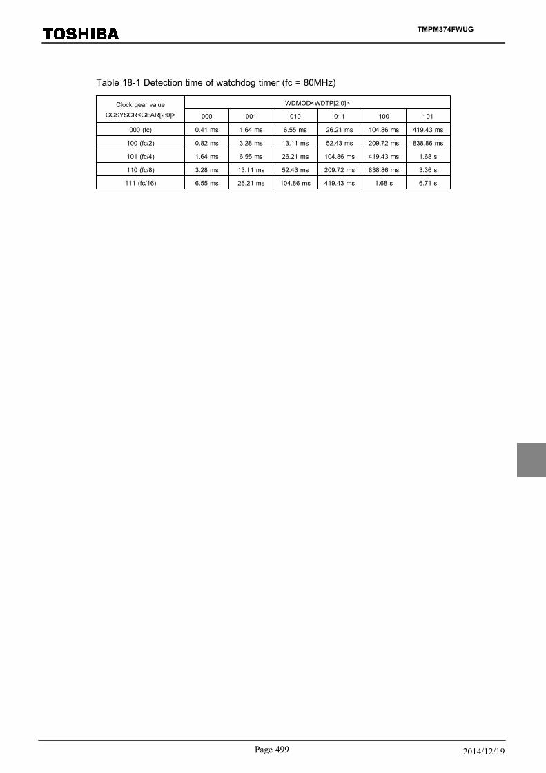
Table 18-1 Detection time of watchdog timer (fc = 80MHz)
Clock gear valueCGSYSCR<GEAR[2:0]>
WDMOD<WDTP[2:0]>
000 001 010 011 100 101
000 (fc) 0.41 ms 1.64 ms 6.55 ms 26.21 ms 104.86 ms 419.43 ms
100 (fc/2) 0.82 ms 3.28 ms 13.11 ms 52.43 ms 209.72 ms 838.86 ms
101 (fc/4) 1.64 ms 6.55 ms 26.21 ms 104.86 ms 419.43 ms 1.68 s
110 (fc/8) 3.28 ms 13.11 ms 52.43 ms 209.72 ms 838.86 ms 3.36 s
111 (fc/16) 6.55 ms 26.21 ms 104.86 ms 419.43 ms 1.68 s 6.71 s
TMPM374FWUG
Page 499 2014/12/19

18.2.2 WDCR (Watchdog Timer Control Register)
31 30 29 28 27 26 25 24
bit symbol - - - - - - - -
After reset 0 0 0 0 0 0 0 0
23 22 21 20 19 18 17 16
bit symbol - - - - - - - -
After reset 0 0 0 0 0 0 0 0
15 14 13 12 11 10 9 8
bit symbol - - - - - - - -
After reset 0 0 0 0 0 0 0 0
7 6 5 4 3 2 1 0
bit symbol WDCR
After reset - - - - - - - -
Bit Bit Symbol Type Function
31-8 − R Read as 0.
7-0 WDCR W Disable/Clear code0xB1:Disable code0x4E: Clear codeOthers:Reserved
TMPM374FWUG
18. Watchdog Timer(WDT)
18.2 Register
Page 5002014/12/19

18.3 Operations
18.3.1 Basic Operation
The Watchdog timer is consists of the binary counters that work using the system clock (fsys) as an input.Detecting time can be selected between 215, 217, 219 , 221, 223 and 225 by the WDMOD<WDTP[2:0]>. The detect-ing time as specified is elapsed, the watchdog timer interrupt (INTWDT) generates, and the watchdog timerout pin (WDTOUT) output "Low".
To detect malfunctions (runaways) of the CPU caused by noise or other disturbances, the binary counterof the watchdog timer should be cleared by software instruction before INTWDT interrupt generates. If the bi-nary counter is not cleared, the non-maskable interrupt generates by INTWDT. Thus CPU detects malfunc-tion (runway), malfunction countermeasure program is performed to return to the normal operation.
Additionally, it is possible to resolve the problem of a malfunction (runaway) of the CPU by connectingthe watchdog timer out pin to reset pins of peripheral devices.
Note:This product does not include a watchdog timer out pin (WDTOUT).
18.3.2 Operation Mode and Status
The watchdog timer begins operation immediately after a reset is cleared.
If not using the watchdog timer, it should be disabled.
The watchdog timer cannot be used as the high-speed frequency clock is stopped. Before transition to be-low modes, the watchdog timer should be disabled.In IDLE mode, its operation depends on the WDMOD<I2WDT> setting.
- STOP mode
Also, the binary counter is automatically stopped during debug mode.
TMPM374FWUG
Page 501 2014/12/19

18.4 Operation when malfunction (runaway) is detected
18.4.1 INTWDT interrupt generation
In the Figure 18-2 shows the case that INTWDT interrupt generates (WDMOD<RESCR>="0").
When an overflow of the binary counter occurs, INTWDT interrupt generates. It is a factor of non-maska-ble interrupt (NMI). Thus CPU detects non-maskable interrupt and performs the countermeasure program.
The factor of non-maskable interrupt is the plural. CGNMIFLG identifies the factor of non-maskable inter-rupts. In the case of INTWDT interrupt, CGNMIFLG<NMIFLG0> is set.
When INTWDT interrupt generates, simultaneously the watchdog timer out (WDTOUT) output "Low".WDTOUT becomes "High" by the watchdog timer clearing that is writing clear code 0x4E to the WDCR reg-ister.
Note:This product does not have the watchdog timer output pin(WDTOUT).
n Overflow 0WDT counter
WDT clear
INTWDT
Write of a clear code
WDTOUT
Figure 18-2 INTWDT interrupt generation
TMPM374FWUG
18. Watchdog Timer(WDT)
18.4 Operation when malfunction (runaway) is detected
Page 5022014/12/19

18.4.2 Internal reset generation
Figure 18-3 shows the internal reset generation (WDMOD<RESCR>="1").
MCU is reset by the overflow of the binary counter. In this case, reset status continues for 32 states. Aclock is initialized so that input clock (fsys) is the same as a internal high-speed frequency clock (fosc). Thismeans fsys = fosc.
n
32-state
WDTOUT
Overflow
WDT counter
Internal reset
INTWDT
Figure 18-3 Internal reset generation
TMPM374FWUG
Page 503 2014/12/19

18.5 Control registerThe watchdog timer (WDT) is controlled by two control registers WDMOD and WDCR.
18.5.1 Watchdog Timer Mode Register (WDMOD)
1. Specifying the detection time of the watchdog timer <WDTP[2:0]>.
Set the watchdog timer detecting time to WDMOD<WDTP[2:0]>. After reset, it is initialized toWDMOD<WDTP[2:0]> = "000".
2. Enabling/disabling the watchdog timer <WDTE>.
When resetting, WDMOD <WDTE> is initialized to "1" and the watchdog timer is enabled.
To disable the watchdog timer to protect from the error writing by the malfunction, first<WDTE> bit is set to "0", and then the disable code (0xB1) must be written to WDCR register.
To change the status of the watchdog timer from "disable" to "enable," set the <WDTE> bit to"1".
3. Watchdog timer out reset connection <RESCR>
This register specifies whether WDTOUT is used for internal reset or interrupt. After reset,WDMOD<RESCR> is initialized to "1", the internal reset is generated by the overflow of binary coun-ter.
18.5.2 Watchdog Timer Control Register(WDCR)
This is a register for disabling the watchdog timer function and controlling the clearing function of the bina-ry counter.
TMPM374FWUG
18. Watchdog Timer(WDT)
18.5 Control register
Page 5042014/12/19

18.5.3 Setting example
18.5.3.1 Disabling control
By writing the disable code (0xB1) to this WDCR register after setting WDMOD <WDTE> to "0," thewatchdog timer can be disabled and the binary counter can be cleared.
7 6 5 4 3 2 1 0
WDMOD ← 0 − − − − − − − Set <WDTE> to "0".
WDCR ← 1 0 1 1 0 0 0 1 Writes the disable code (0xB1).
18.5.3.2 Enabling control
Set WDMOD <WDTE> to "1".
7 6 5 4 3 2 1 0
WDMOD ← 1 − − − − − − − Set <WDTE> to "1".
18.5.3.3 Watchdog timer clearing control
Writing the clear code (0x4E) to the WDCR register clears the binary counter and it restarts counting.
7 6 5 4 3 2 1 0
WDCR ← 0 1 0 0 1 1 1 0 Writes the clear code (0x4E).
18.5.3.4 Detection time of watchdog timer
In the case that 221/fsys is used, set "011" to WDMOD<WDTP[2:0]>.
7 6 5 4 3 2 1 0
WDMOD ← 1 0 1 1 − − − −
TMPM374FWUG
Page 505 2014/12/19

TMPM374FWUG
18. Watchdog Timer(WDT)
18.5 Control register
Page 5062014/12/19

19. Flash
This section describes the hardware configuration and operation of the flash memory.
19.1 Flash Memory
19.1.1 Features
1. Memory capacity
TMPM374FWUG contains flash memory. The memory sizes and configurations are shown inthe table below.
Independent write access to each block is available. When the CPU is to access the internal flashmemory, 32-bit data bus width is used.
2. Write / erase time
Writing is executed per page. TMPM374FWUG contains 64 words.
Page writing requires 1.25ms (typical) regardless of number of words.
A block erase requires 0.1 sec. (typical).
The following table shows write and erase time per chip.
Product Name Memory sizeBlock Configuration
# of words Write time Erase time128 KB 64 KB 32 KB 16 KB
TMPM374FWUG 128 KB 0 1 1 2 64 0.64 sec 0.4 sec
Note: The above values are theoretical values not including data transfer time. The write time per chip de-pends on the write method to be used by users.
3. Programming method
There are two types of the onboard programming mode for users to program (rewrite) the devicewhile it is mounted on the user's board:
a. User boot mode
The use’s original rewriting method can be supported.b. Single boot mode
The rewriting method to use serial data transfer (Toshiba's unique method) can be supported.
TMPM374FWUG
Page 507 2014/12/19
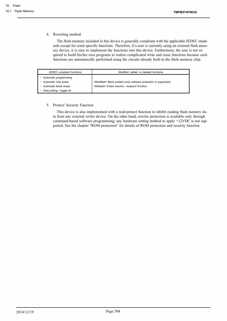
4. Rewriting method
The flash memory included in this device is generally compliant with the applicable JEDEC stand-ards except for some specific functions. Therefore, if a user is currently using an external flash mem-ory device, it is easy to implement the functions into this device. Furthermore, the user is not re-quired to build his/her own programs to realize complicated write and erase functions because suchfunctions are automatically performed using the circuits already built-in the flash memory chip.
JEDEC compliant functions Modified, added, or deleted functions
・ Automatic programming・ Automatic chip erase・ Automatic block erase・ Data polling / toggle bit
<Modified> Block protect (only software protection is supported)<Deleted> Erase resume - suspend function
5. Protect/ Security Function
This device is also implemented with a read-protect function to inhibit reading flash memory da-ta from any external writer device. On the other hand, rewrite protection is available only throughcommand-based software programming; any hardware setting method to apply +12VDC is not sup-ported. See the chapter "ROM protection" for details of ROM protection and security function.
TMPM374FWUG
19. Flash
19.1 Flash Memory
Page 5082014/12/19
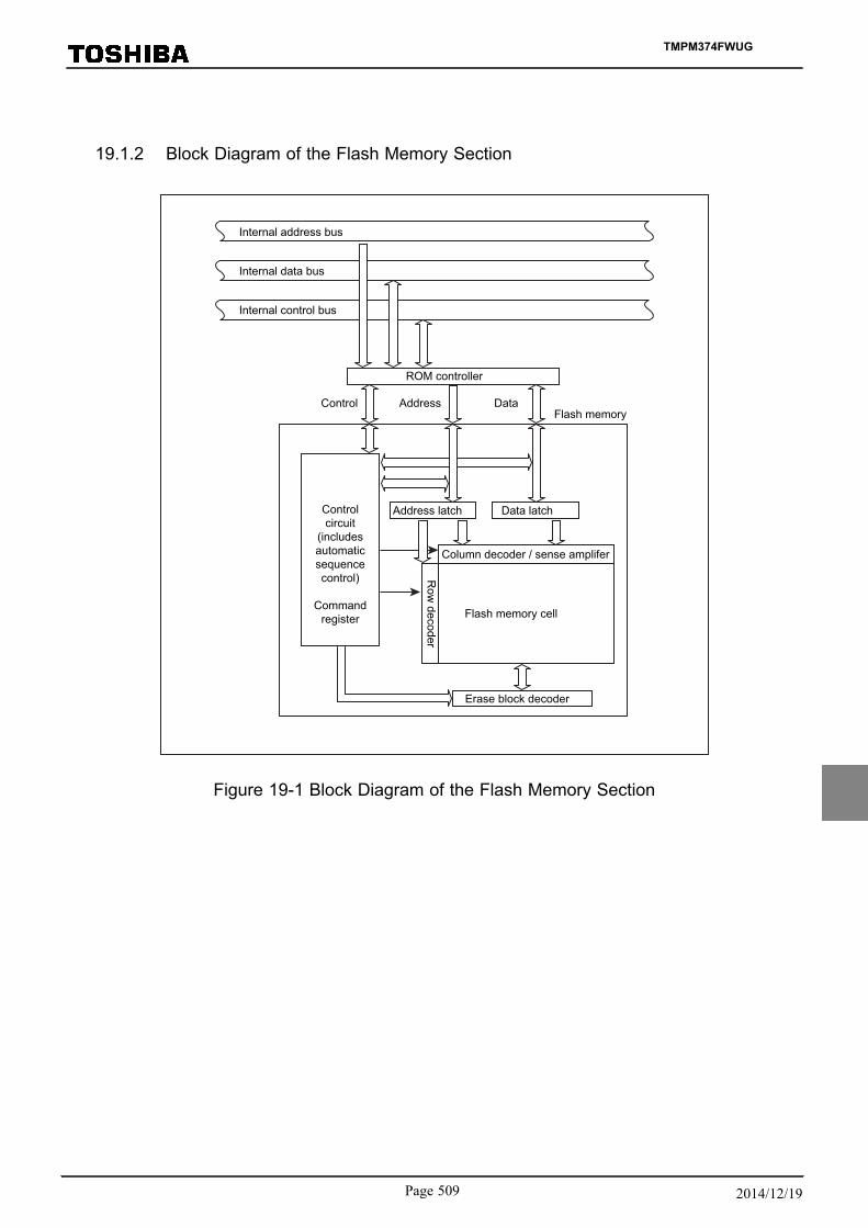
19.1.2 Block Diagram of the Flash Memory Section
Internal address bus
Internal data bus
Internal control bus
Control Address DataFlash memory
ROM controller
Controlcircuit
(includesautomaticsequencecontrol)
Commandregister
Address latch Data latch
Column decoder / sense amplifer
Row
decoder
Flash memory cell
Erase block decoder
Figure 19-1 Block Diagram of the Flash Memory Section
TMPM374FWUG
Page 509 2014/12/19
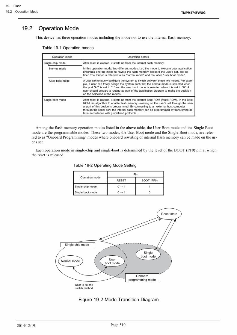
19.2 Operation ModeThis device has three operation modes including the mode not to use the internal flash memory.
Table 19-1 Operation modes
Operation mode Operation details
Single chip mode After reset is cleared, it starts up from the internal flash memory.
Normal mode In this operation mode, two different modes, i.e., the mode to execute user applicationprograms and the mode to rewrite the flash memory onboard the user’s set, are de-fined.The former is referred to as "normal mode" and the latter "user boot mode".
User boot mode A user can uniquely configure the system to switch between these two modes. For exam-ple, a user can freely design the system such that the normal mode is selected whenthe port "A0" is set to "1" and the user boot mode is selected when it is set to "0". Auser should prepare a routine as part of the application program to make the decisionon the selection of the modes.
Single boot mode After reset is cleared, it starts up from the internal Boot ROM (Mask ROM). In the BootROM, an algorithm to enable flash memory rewriting on the user’s set through the seri-al port of this device is programmed. By connecting to an external host computerthrough the serial port, the internal flash memory can be programmed by transferring da-ta in accordance with predefined protocols.
Among the flash memory operation modes listed in the above table, the User Boot mode and the Single Bootmode are the programmable modes. These two modes, the User Boot mode and the Single Boot mode, are refer-red to as "Onboard Programming" modes where onboard rewriting of internal flash memory can be made on the us-er's set.
Each operation mode in single-chip and single-boot is determined by the level of the BOOT (PF0) pin at whichthe reset is released.
Table 19-2 Operating Mode Setting
Operation modePin
RESET BOOT (PF0)
Single chip mode 0 → 1 1
Single boot mode 0 → 1 0
User to set theswitch method
Normal mode Userboot mode
Reset state
Singleboot mode
Onboardprogramming mode
Single chip mode
Figure 19-2 Mode Transition Diagram
TMPM374FWUG
19. Flash
19.2 Operation Mode
Page 5102014/12/19

19.2.1 Reset Operation
To reset the device, ensure that the power supply voltage is within the operating voltage range, that the inter-nal oscillator has been stabilized, and that the RESET input is held at "0" for a minimum duration of 12 sys-tem clocks (0.15μs with 80MHz operation; the "1/1" clock gear mode is applied after reset).
Note 1: It is necessary to apply "0" to the RESET inputs upon power on for a minimum duration of 3.2msec regardless of the operating frequency.
Note 2: While flash auto programming or erasing is in progress, at least 0.5 μs of reset period is re-quired regardless of the system clock frequency. In this condition, it takes approx. 2 ms to ena-ble reading after reset.
19.2.2 User Boot Mode (Single chip mode)
User Boot mode is to use flash memory programming routine defined by users. It is used when the data trans-fer buses for flash memory program code on the old application and for serial I/O are different. It operates atthe single chip mode; therefore, a switch from normal mode in which user application is activated at the sin-gle chip mode to User Boot Mode for programming flash is required. Specifically, add a mode judgment rou-tine to a reset program in the user application.
The condition to switch the modes needs to be set by using the I/O of TMPM374FWUG in conformitywith the user’s system setup condition. Also, flash memory programming routine that the user uniquelymakes up needs to be set in the new application. This routine is used for programming after being switchedto User Boot Mode. The execution of the programming routine must take place while it is stored in the area oth-er than the flash memory since the data in the internal flash memory cannot be read out during delete / writ-ing mode. Once re-programming is complete, it is recommended to protect relevant flash blocks from acciden-tal corruption during subsequent Single-Chip (Normal mode) operations. Be sure not to cause any exceptionsincluding a non-maskable while User Boot Mode.
(1-A) and (1-B) are the examples of programming with routines in the internal flash memory and in the ex-ternal memory. For a detailed description of the erase and program sequence, refer to "19.3 On-board Program-ming of Flash Memory (Rewrite/Erase)".
TMPM374FWUG
Page 511 2014/12/19

19.2.2.1 (1-A) Method 1: Storing a Programming Routine in the Flash Memory
(1) Step-1
Determine the conditions (e.g., pin states) required for the flash memory to enter User Boot modeand the I/O bus to be used to transfer new program code. Create hardware and software according-ly. Before installing the TMPM374FWUG on a printed circuit board, write the following program rou-tines into an arbitrary flash block using programming equipment.
(a) Mode judgment routine: Code to determine whether or not to switch to User Boot mode
(b) Programming routine: Code to download new program code from a host controllerand re-program the flash memory
(c) Copy routine: Code to copy the data described in (b) from theTMPM374FWUG flash memory to either theTMPM374FWUG on-chip RAM or external memory device.
New ApplicationProgram Code
Old ApplicationProgram Code
Flash memory
(Host)
(I/O)
RAM
[Reset Procedure](a) Mode Judgement Routine
(b) Programming Routine
(c) Copy Routine
(TMPM374FWUG)
TMPM374FWUG
19. Flash
19.2 Operation Mode
Page 5122014/12/19

(2) Step-2
The following description is the case that programming routines are installed in the reset process-ing program. After RESET pin is released, the reset procedure determines whether to put theTMPM374FWUG flash memory in User Boot mode. If mode switching conditions are met, theflash memory enters User Boot mode. (All interrupts including NMI must be not used while inUser Boot mode.)
New ApplicationProgram Code
Old ApplicationProgram Code
Flash memory
(Host)
(I/O)
RAM
[Reset Procedure](a) Mode Judgement Routine
(b) Programmming Routine
(c) Copy Routine
0 → 1 RESET
Conditions forentering User Bootmode (defined bythe user)
(TMPM374FWUG)
(3) Step-3
Once transition to User Boot mode is occurred, execute the copy routine (c) to copy the flash pro-gramming routine (b) to the TMPM374FWUG on-chip RAM.
New ApplicationProgram Code
Old ApplicationProgram Code
Flash memory
(Host)
(I/O)
RAM
[Reset Procedure](a) Mode Judgement Routine
(b) Programming Routine
(c) Copy Routine
(b) Programming Routine
(TMPM374FWUG)
TMPM374FWUG
Page 513 2014/12/19

(4) Step-4
Jump program execution to the flash programming routine in the on-chip RAM to clear write orerase protection and erase a flash block containing the old application program code.
New ApplicationProgram Code
Flash memory
(Host)
(I/O)
RAM
[Reset Procedure](a) Mode Judgement Routine
(b) Programming Routine
(c) Copy Routine
(b) Programming Routine
(Erased)
(TMPM374FWUG)
(5) Step-5
Continue executing the flash programming routine to download new program code from the hostcontroller and program it into the erased flash block. When the programming is completed, the writ-ing or erase protection of that flash block in the user’s program area must be set.
New ApplicationProgram Code
New ApplicationProgram Code
Flash memory
(Host)
(I/O)
RAM
[Reset Procedure](a) Mode Judgement Routine
(b) Programming Routine
(c) Copy Routine
(b) Programming Routine
(TMPM374FWUG)
TMPM374FWUG
19. Flash
19.2 Operation Mode
Page 5142014/12/19

(6) Step-6
Set RESET to "0" to reset the TMPM374FWUG. Upon reset, the on-chip flash memory is set to Nor-mal mode. After RESET is released, the CPU will start executing the new application program code.
New ApplicationProgram Code
Flash memory
(Host)
(I/O)
RAM
[Reset Procedure](a) Mode Judgement Routine
(b) Programming Routine
(c) Copy Routine
0 → 1 RESET
Set to Normal mode
(TMPM374FWUG)
TMPM374FWUG
Page 515 2014/12/19

19.2.2.2 (1-B) Method 2: Transferring a Programming Routine from an External Host
(1) Step-1
Determine the conditions (e.g., pin states) required for the flash memory to enter User Boot modeand the I/O bus to be used to transfer new program code. Create hardware and software according-ly. Before installing the TMPM374FWUG on a printed circuit board, write the following program rou-tines into an arbitrary flash block using programming equipment.
(a) Mode judgment routine: Code to determine whether or not to switch to User Boot mode
(b) Transfer routine: Code to download new program code from a host controller
Also, prepare a programming routine shown below on the host controller:
(c) Programming routine: Code to download new program code from an external hostcontroller and re-program the flash memory
New ApplicationProgram Code
Flash memory
( )
(I/O)
RAM
[Reset Procedure]
(a) Mode Judgement Routine
(b) Transfer Routine
Old ApplicationProgram Code
(c) Programming Routine
(TMPM374FWUG)
TMPM374FWUG
19. Flash
19.2 Operation Mode
Page 5162014/12/19

(2) Step-2
The following description is the case that programming routines are installed in the reset process-ing program. After RESET is released, the reset procedure determines whether to put theTMPM374FWUG flash memory in User Boot mode. If mode switching conditions are met, theflash memory enters User Boot mode. (All interrupts including NMI must be not used while inUser Boot mode).
New ApplicationProgram Code
Flash memory
(Host)
(I/O)
RAM
[Reset Procedure]
(a) Mode Judgement Routine
(b) Transfer Routine
Old ApplicationProgram Code
(c)Programming Routine
0 → 1 RESET
Conditions forentering User Bootmode (defined bythe user)
(TMPM374FWUG)
(3) Step-3
Once User Boot mode is entered, execute the transfer routine (b) to download the flash program-ming routine (c) from the host controller to the TMPM374FWUG on-chip RAM.
New ApplicationProgram Code
Flash memory
( )
(I/O)
RAM
[Reset Procedure]
(a) Mode Judgement Routine
(b) Transfer Routine
Old ApplicationProgram Code
(c) Programming Routine
(c) Programming Routine
(TMPM374FWUG)
TMPM374FWUG
Page 517 2014/12/19
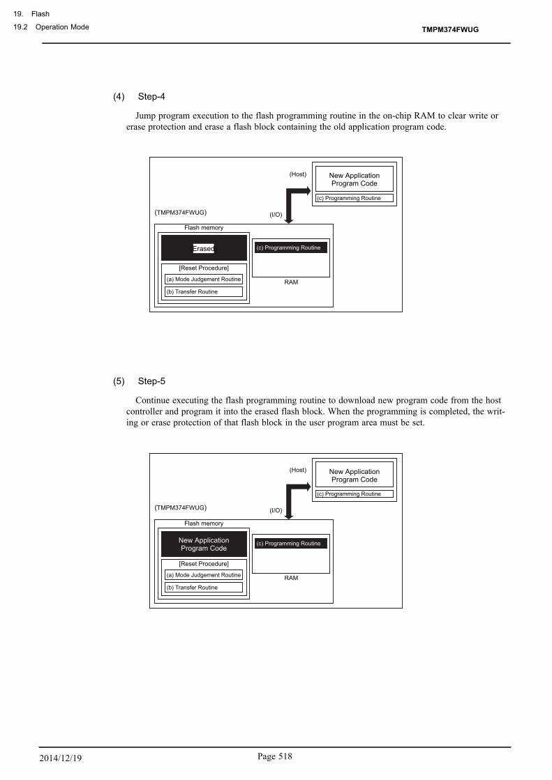
(4) Step-4
Jump program execution to the flash programming routine in the on-chip RAM to clear write orerase protection and erase a flash block containing the old application program code.
New ApplicationProgram Code
Flash memory
(Host)
(I/O)
RAM
[Reset Procedure]
(a) Mode Judgement Routine
(b) Transfer Routine
(c) Programming Routine
(c) Programming Routine(Erased)
(TMPM374FWUG)
(5) Step-5
Continue executing the flash programming routine to download new program code from the hostcontroller and program it into the erased flash block. When the programming is completed, the writ-ing or erase protection of that flash block in the user program area must be set.
New ApplicationProgram Code
Flash memory
(Host)
(I/O)
RAM
[Reset Procedure]
(a) Mode Judgement Routine
(b) Transfer Routine
New ApplicationProgram Code
(c) Programming Routine
(c) Programming Routine
(TMPM374FWUG)
TMPM374FWUG
19. Flash
19.2 Operation Mode
Page 5182014/12/19
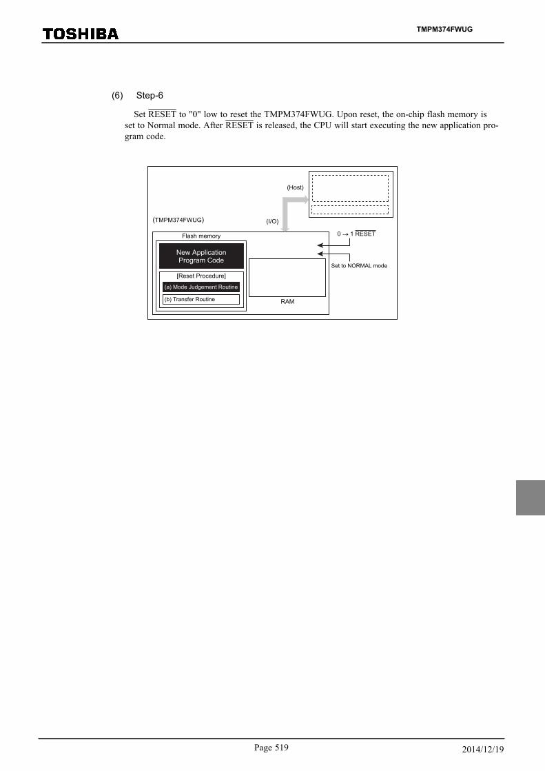
(6) Step-6
Set RESET to "0" low to reset the TMPM374FWUG. Upon reset, the on-chip flash memory isset to Normal mode. After RESET is released, the CPU will start executing the new application pro-gram code.
Flash memory
(Host)
(I/O)
RAM
[Reset Procedure]
(a) Mode Judgement Routine
(b) Transfer Routine
New ApplicationProgram Code
0 → 1 RESET
Set to NORMAL mode
(TMPM374FWUG)
TMPM374FWUG
Page 519 2014/12/19

19.2.3 Single Boot Mode
In Single Boot mode, the flash memory can be re-programmed by using a program contained in theTMPM374FWUG on-chip boot ROM. This boot ROM is a masked ROM. When Single Boot mode is selec-ted upon reset, the boot ROM is mapped to the address region including the interrupt vector table while theflash memory is mapped to an address region different from it.
Single Boot mode allows for serial programming of the flash memory. Channel 0 of the SIO (SIO0) of theTMPM374FWUG is connected to an external host controller. Via this serial link, a programming routine isdownloaded from the host controller to the TMPM374FWUG on-chip RAM. Then, the flash memory is re-pro-grammed by executing the programming routine. The host sends out both commands and programming datato re-program the flash memory. Communications between the SIO0 and the host must follow the protocol de-scribed later. To secure the contents of the flash memory, the validity of the application’s password is veri-fied before a programming routine is downloaded into the on-chip RAM. If password matching fails, the trans-fer of a programming routine itself is aborted. As in the case of User Boot mode, all interrupts including thenon-maskable interrupt (NMI) must be disabled in Single Boot mode while the flash memory is being erasedor programmed. In Single Boot mode, the boot-ROM programs are executed in Normal mode.
Once re-programming is complete, it is recommended to set the write/erase protection to the relevant flashblocks from accidental corruption during subsequent Single-Chip (Normal mode) operations.
19.2.3.1 (2-A) Using the Program in the On-Chip Boot ROM
(1) Step-1
The flash block containing the old version of the program code does not need to be erased beforeexecuting the programming routine. Since a programming routine and programming data are transfer-red via the SIO (SIO0), the SIO0 must be connected to a host controller. Prepare a programming rou-tine (a) on the host controller.
New Application Program Code
Flash memory
(Host)
(I/O)
RAM
Boot ROM
Old Application Program Code
(or erased state)
SIO0
(a)Programming Routine
(TMPM374FWUG)
TMPM374FWUG
19. Flash
19.2 Operation Mode
Page 5202014/12/19

(2) Step-2
Set the RESET pin to "1" to cancel the reset of the TMPM374FWUG when the BOOT pin has al-ready been set to "0". After reset, CPU reboots from the on-chip boot ROM. The 12-byte passwordtransferred from the host controller via SIO0 is firstly compared to the contents of the special flashmemory locations. (If the flash block has already been erased, the password is 0xFF).
New Application Proram Code
Flash memory
(Host)
(I/O)
RAM
(a) Programming Routine
Boot ROM
Old Application Program Code
(or erased state)
SIO0
0 → 1 RESET
0 BOOT
(TMPM374FWUG)
(3) Step-3
If the password is correct, the boot program downloads the programming routine (a) from thehost controller into the on-chip RAM of the TMPM374FWUG. The programming routine must be stor-ed in the range from 0x2000_0400 to the end address of RAM.
New Application Program Code
Flash memory
(Host)
(I/O)
RAM
Boot ROM
Old Application Program Code
(or erased state)
SIO0
(a) Programming Routine
(a) Programming Routine
(TMPM374FWUG)
TMPM374FWUG
Page 521 2014/12/19

(4) Step-4
The CPU jumps to the programming routine (a) in the on-chip RAM to erase the flash block contain-ing the old application program code. The Block Erase or Chip Erase command may be used.
( )
(I/O)
RAM
SIO0
(a) Programming Routine
(a)
(TMPM374FWUG)
(5) Step-5
Next, the programming routine (a) downloads new application program code from the host control-ler and programs it into the erased flash block. When the programming is completed, the writing orerase protection of that flash block in the user’s program area must be set.
In the example below, new program code comes from the same host controller via the same SIO0channel as for the programming routine. However, once the programming routine has begun to exe-cute in the on-chip RAM, it is free to change the transfer path and the source of the transfer. Createboard hardware and a programming routine to suit your particular needs.
New Application Program Code
Flash memory
(Host)
(I/O)
RAM
Boot ROM
New Application Program Code
SIO0
(a) Programming Routine
(a) Programming Routine
(TMPM374FWUG)
TMPM374FWUG
19. Flash
19.2 Operation Mode
Page 5222014/12/19
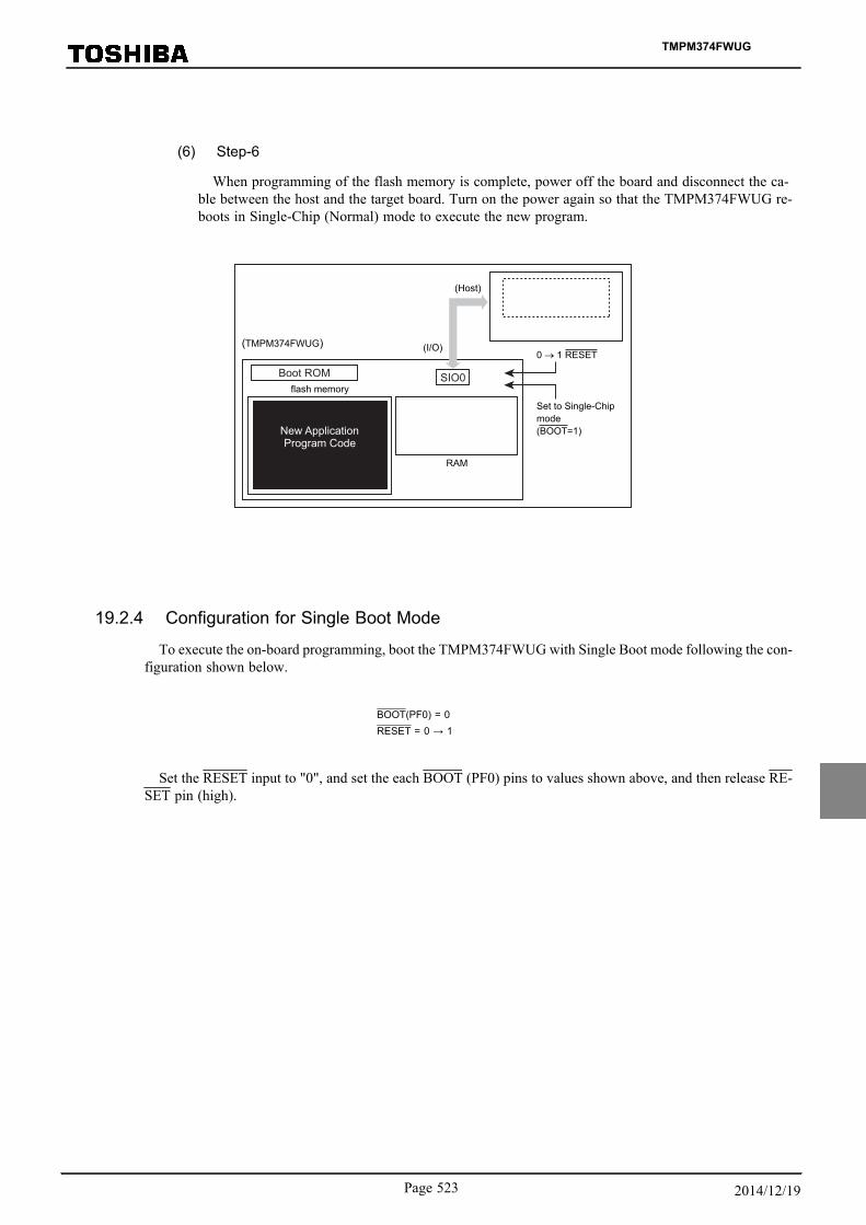
(6) Step-6
When programming of the flash memory is complete, power off the board and disconnect the ca-ble between the host and the target board. Turn on the power again so that the TMPM374FWUG re-boots in Single-Chip (Normal) mode to execute the new program.
flash memory
(Host)
(I/O)
RAM
Boot ROM
New Application Program Code
SIO0
0 → 1 RESET
Set to Single-Chip mode (BOOT=1)
(TMPM374FWUG)
19.2.4 Configuration for Single Boot Mode
To execute the on-board programming, boot the TMPM374FWUG with Single Boot mode following the con-figuration shown below.
BOOT(PF0) = 0RESET = 0 → 1
Set the RESET input to "0", and set the each BOOT (PF0) pins to values shown above, and then release RE-SET pin (high).
TMPM374FWUG
Page 523 2014/12/19

19.2.5 Memory Map
Figure 19-3 shows a comparison of the memory maps in Normal and Single Boot modes. In Single Bootmode, the internal flash memory is mapped to 0x3F80_0000 and later addresses, and the Internal boot ROM(Mask ROM) is mapped to 0x0000_0000 through 0x0000_0FFF.
The internal flash memory and RAM addresses of each device are shown below.
Product Name Flash Size RAM SizeFlash Address
(Single Chip / Single Boot Mode)RAM Address
TMPM374FWUG 128 KB 6 KB0x0000_0000 to 0x0001_FFFF0x3F80_0000 to 0x3F81_FFFF
0x2000_0000 to 0x2000_17FF
0xFFFF_FFFFSingle Chip Mode
Internal RAM(6 KB)
Internal Flash ROM(128 KB)
0x2000_17FF
0x2000_0000
0x0001_FFFF
0x0000_0000
SFR0x41FF_FFFF
0x4000_0000
0xFFFF_FFFFSingle Boot Mode
Internal RAM(6 KB)
Internal BOOT ROM(4 KB)
0x2000_17FF
0x2000_0000
0x0000_0FFF
0x0000_0000
SFR0x41FF_FFFF
0x4000_0000
Internal Flash ROM(128 KB)
0x3F81_FFFF
0x3F80_0000Reserved 0x3F7F_F000
Figure 19-3 Memory Maps for TMPM374FWUG
TMPM374FWUG
19. Flash
19.2 Operation Mode
Page 5242014/12/19

19.2.6 Interface specification
In Single Boot mode, an SIO channel is used for communications with a programming controller. Thesame configuration is applied to a communication format on a programming controller to execute the on-board programming. Both UART (asynchronous) and I/O Interface (synchronous) modes are supported. Thecommunication formats are shown below.
・ UART communication
Communication channel : SIO channel 0
Serial transfer mode : UART (asynchronous) mode, half -duplex, LSB first
Data length : 8 bits
Parity bit : None
STOP bit : 1 bit
Baud rate : Arbitrary baud rate
・ I/O Interface mode
Communication channel : SIO channel 0
Serial transfer mode : I/O interface mode, full -duplex, LSB first
Synchronization clock (SCLK0) : Input mode
Handshaking signal : PE4 configured as an output mode
Baud rate : Arbitrary baud rate
Table 19-3 Required Pin Connections
PinInterface
UART I/O Interface Mode
Power supply pins
DVDD5 ο ο
DVSS ο ο
AVDD5B ο ο
AVSSB ο ο
VOUT3 ο ο
VOUT15 ο ο
RVDD5 ο ο
Mode-setting pin BOOT (PF0) ο ο
Reset pin RESET ο ο
Communicationpin
TXD0 (PE0) ο ο
RXD0 (PE1) ο ο
SCLK0 (PE2) × ο (Input mode)
PE4 × ο (Output mode)
ο:Necessary×:Unnecessary
TMPM374FWUG
Page 525 2014/12/19

19.2.7 Data Transfer Format
Table 19-4, Table 19-6 to Table 19-7 illustrate the operation commands and data transfer formats at each op-eration mode. In conjunction with this section, refer to "19.2.10 Operation of Boot Program".
Table 19-4 Single Boot Mode Commands
Code Command
0x10 RAM transfer
0x40 Chip and protection bit erase
19.2.8 Restrictions on internal memories
Single Boot Mode places restrictions on the internal RAM and ROM as shown in Table 19-5.
Table 19-5 Restrictions in Single Boot Mode
Memory Details
Internal RAMA program contained in the BOOT ROM uses the area, through 0x2000_0000 to0x2000_03FF, as a work area.Store the RAM transfer program from 0x2000_0400 through the end address of RAM.
Internal ROMThe following addresses are assigned for storing software ID information and passwords.Storing program in these addresses is not recommendable.0x3F81_FFF0 to 0x3F81_FFFF
19.2.9 Transfer Format for Boot Program
The following tables shows the transfer format for each Boot program command. Use this section in conjunc-tion with Chapter "19.2.10 Operation of Boot Program".
TMPM374FWUG
19. Flash
19.2 Operation Mode
Page 5262014/12/19

19.2.9.1 RAM Transfer
Table 19-6 Transfer Format for the RAM Transfer Command
Byte Data Transferred from the Controller to theTMPM374FWUG Baud rate Data Transferred from the TMPM374FWUG to
the Controller
BootROM
1 byte Serial operation mode and baud rateFor UART mode : 0x86For I/O Interface mode : 0x30
Desired baudrate (Note 1)
−
2 byte − ACK for the serial operation mode byte・For UART mode- Normal acknowledge : 0x86(The boot program aborts if the baud rate cannot be set correctly.)・For I/O Interface mode- Normal acknowledge :0x30
3 byte Command code (0x10) −
4 byte − ACK for the command code byte (Note 2)- Normal acknowledge : 0x10- Negative acknowledge : 0xX1- Communication error : 0xX8
5 byteto16 byte
Password sequence (12 bytes))0x3F81_FFF4 to 0x3F81_FFFF
−
17 byte Check SUM value for bytes 5 to 16 −
18 byte − ACK for the checksum byte (Note 2)- Normal acknowledge : 0x10- Negative acknowledge : 0xX1- Communication error : 0xX8
19 byte RAM storage start address 31 to 24 −
20 byte RAM storage start address 23 to 16 −
21 byte RAM storage start address 15 to 8 −
22 byte RAM storage start address 7 to 0 −
23 byte RAM storage start address 15 to 8 −
24 byte RAM storage start address 7 to 0 −
25 byte Check SUM value for bytes 19 to 24 −
26 byte − ACK for the checksum byte (Note 2)- Normal acknowledge : 0x10- Negative acknowledge : 0xX1- Communication error : 0xX8
27 bytetombyte
RAM storage data −
m+ 1 byte Checksum value for bytes 27 to m −
m+ 2 byte − ACK for the checksum byte (Note 2)- Normal acknowledge : 0x10- Negative acknowledge : 0xX1- Communication error : 0xX8
RAM m+ 3 byte − Jump to RAM storage start address
Note 1: In I/O Interface mode, the baud rate for the transfers of the first and second bytes must be 1/16 ofthe desired baud rate.
Note 2: In case of any negative acknowledge, the boot program returns to a state in which it waits for a com-mand code (3rd byte). In I/O Interface mode, if a communication error occurs, a negative acknowl-edge does not occur.
Note 3: The 19th to 25th bytes must be within the RAM address range from 0x2000_0400 through the end ad-dress of RAM.
TMPM374FWUG
Page 527 2014/12/19
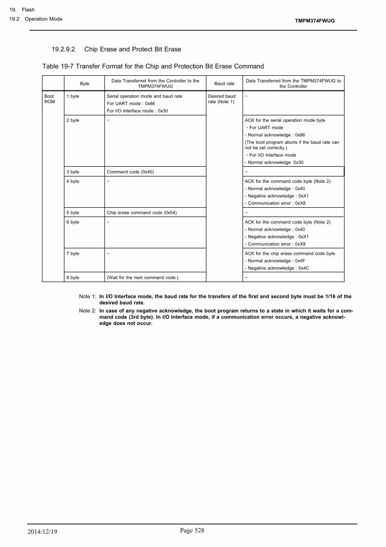
19.2.9.2 Chip Erase and Protect Bit Erase
Table 19-7 Transfer Format for the Chip and Protection Bit Erase Command
Byte Data Transferred from the Controller to theTMPM374FWUG Baud rate Data Transferred from the TMPM374FWUG to
the Controller
BootROM
1 byte Serial operation mode and baud rateFor UART mode : 0x86For I/O Interface mode : 0x30
Desired baudrate (Note 1)
−
2 byte − ACK for the serial operation mode byte・For UART mode- Normal acknowledge : 0x86(The boot program aborts if the baud rate cannot be set correctly.)・For I/O Interface mode- Normal acknowledge :0x30
3 byte Command code (0x40) −
4 byte − ACK for the command code byte (Note 2)- Normal acknowledge : 0x40- Negative acknowledge : 0xX1- Communication error : 0xX8
5 byte Chip erase command code (0x54) −
6 byte − ACK for the command code byte (Note 2)- Normal acknowledge : 0x40- Negative acknowledge : 0xX1- Communication error : 0xX8
7 byte − ACK for the chip erase command code byte- Normal acknowledge : 0x4F- Negative acknowledge : 0x4C
8 byte (Wait for the next command code.) −
Note 1: In I/O Interface mode, the baud rate for the transfers of the first and second byte must be 1/16 of thedesired baud rate.
Note 2: In case of any negative acknowledge, the boot program returns to a state in which it waits for a com-mand code (3rd byte). In I/O Interface mode, if a communication error occurs, a negative acknowl-edge does not occur.
TMPM374FWUG
19. Flash
19.2 Operation Mode
Page 5282014/12/19
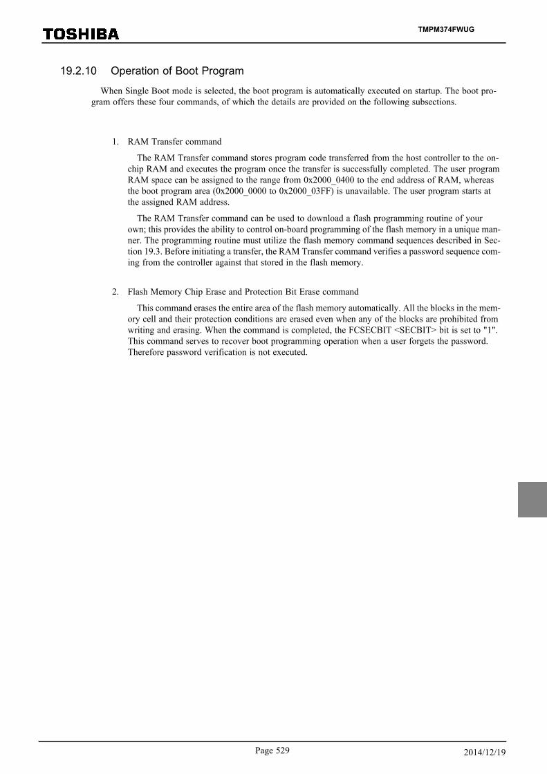
19.2.10 Operation of Boot Program
When Single Boot mode is selected, the boot program is automatically executed on startup. The boot pro-gram offers these four commands, of which the details are provided on the following subsections.
1. RAM Transfer command
The RAM Transfer command stores program code transferred from the host controller to the on-chip RAM and executes the program once the transfer is successfully completed. The user programRAM space can be assigned to the range from 0x2000_0400 to the end address of RAM, whereasthe boot program area (0x2000_0000 to 0x2000_03FF) is unavailable. The user program starts atthe assigned RAM address.
The RAM Transfer command can be used to download a flash programming routine of yourown; this provides the ability to control on-board programming of the flash memory in a unique man-ner. The programming routine must utilize the flash memory command sequences described in Sec-tion 19.3. Before initiating a transfer, the RAM Transfer command verifies a password sequence com-ing from the controller against that stored in the flash memory.
2. Flash Memory Chip Erase and Protection Bit Erase command
This command erases the entire area of the flash memory automatically. All the blocks in the mem-ory cell and their protection conditions are erased even when any of the blocks are prohibited fromwriting and erasing. When the command is completed, the FCSECBIT <SECBIT> bit is set to "1".This command serves to recover boot programming operation when a user forgets the password.Therefore password verification is not executed.
TMPM374FWUG
Page 529 2014/12/19

19.2.10.1 RAM Transfer Command
See Table 19-6 for the transfer format of this command.
1. The 1st byte specifies which one of the two serial operation modes is used. For a detailed descrip-tion of how the serial operation mode is determined, see "19.2.10.4 Determination of a Serial Op-eration Mode" described later. If the mode is determined as UART mode, the boot programchecks if the baud rate setting can be performed. During the first-byte processing, receiving op-eration is prohibited. (SC0MOD0<RXE>=0)
・ To communicate in UART mode
The 1st byte is set to "0x86" and is transmitted from the controller to the target boardat the specified baud rate by setting UART. If the serial operation mode is determined asUART, then the boot program checks if the baud rate setting can be performed. If thatbaud rate cannot be set, the boot program aborts and any subsequent communications can-not be done. Please refer to "Baud rate setting" for the method of judging whether the set-ting of the baud rate is possible.
・ To communicate in I/O Interface mode
The 1st byte is set to "0x30" and is transmitted from the controller to the target boardat 1/16 of the desired baud rate by the synchronous setting. Same as the 1st byte, a 1/16of the specified baud rate is used in the 2nd transmission. From the 3rd byte (operation com-mand data), users can transmit data at specified baud rate.
In I/O interface mode, CPU considers the reception terminal to be an input port and mon-itors the level of I/O port. If the baud rate is high or operation frequency is high, CPUmay not distinguish the level of I/O port. To avoid this situation, the baud rate is set atthe 1/16 of desired baud rate in the I/O interface. When the serial operation mode is deter-mined as I/O Interface mode, SCLK Input mode is set. The controller must ensure thatits AC timing restrictions are satisfied at the selected baud rate. In the case of I/O Inter-face mode, the boot program does not check the receive error flag; thus there is no error ac-knowledge responce (bit 3, 0x08).
TMPM374FWUG
19. Flash
19.2 Operation Mode
Page 5302014/12/19
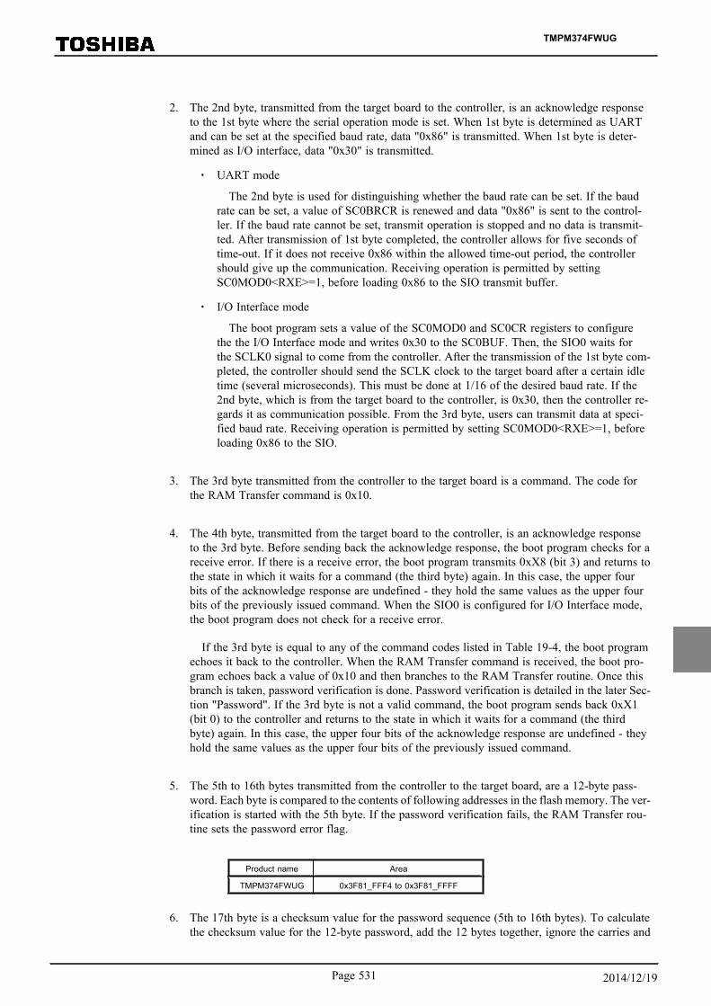
2. The 2nd byte, transmitted from the target board to the controller, is an acknowledge responseto the 1st byte where the serial operation mode is set. When 1st byte is determined as UARTand can be set at the specified baud rate, data "0x86" is transmitted. When 1st byte is deter-mined as I/O interface, data "0x30" is transmitted.
・ UART mode
The 2nd byte is used for distinguishing whether the baud rate can be set. If the baudrate can be set, a value of SC0BRCR is renewed and data "0x86" is sent to the control-ler. If the baud rate cannot be set, transmit operation is stopped and no data is transmit-ted. After transmission of 1st byte completed, the controller allows for five seconds oftime-out. If it does not receive 0x86 within the allowed time-out period, the controllershould give up the communication. Receiving operation is permitted by settingSC0MOD0<RXE>=1, before loading 0x86 to the SIO transmit buffer.
・ I/O Interface mode
The boot program sets a value of the SC0MOD0 and SC0CR registers to configurethe the I/O Interface mode and writes 0x30 to the SC0BUF. Then, the SIO0 waits forthe SCLK0 signal to come from the controller. After the transmission of the 1st byte com-pleted, the controller should send the SCLK clock to the target board after a certain idletime (several microseconds). This must be done at 1/16 of the desired baud rate. If the2nd byte, which is from the target board to the controller, is 0x30, then the controller re-gards it as communication possible. From the 3rd byte, users can transmit data at speci-fied baud rate. Receiving operation is permitted by setting SC0MOD0<RXE>=1, beforeloading 0x86 to the SIO.
3. The 3rd byte transmitted from the controller to the target board is a command. The code forthe RAM Transfer command is 0x10.
4. The 4th byte, transmitted from the target board to the controller, is an acknowledge responseto the 3rd byte. Before sending back the acknowledge response, the boot program checks for areceive error. If there is a receive error, the boot program transmits 0xX8 (bit 3) and returns tothe state in which it waits for a command (the third byte) again. In this case, the upper fourbits of the acknowledge response are undefined - they hold the same values as the upper fourbits of the previously issued command. When the SIO0 is configured for I/O Interface mode,the boot program does not check for a receive error.
If the 3rd byte is equal to any of the command codes listed in Table 19-4, the boot programechoes it back to the controller. When the RAM Transfer command is received, the boot pro-gram echoes back a value of 0x10 and then branches to the RAM Transfer routine. Once thisbranch is taken, password verification is done. Password verification is detailed in the later Sec-tion "Password". If the 3rd byte is not a valid command, the boot program sends back 0xX1(bit 0) to the controller and returns to the state in which it waits for a command (the thirdbyte) again. In this case, the upper four bits of the acknowledge response are undefined - theyhold the same values as the upper four bits of the previously issued command.
5. The 5th to 16th bytes transmitted from the controller to the target board, are a 12-byte pass-word. Each byte is compared to the contents of following addresses in the flash memory. The ver-ification is started with the 5th byte. If the password verification fails, the RAM Transfer rou-tine sets the password error flag.
Product name Area
TMPM374FWUG 0x3F81_FFF4 to 0x3F81_FFFF
6. The 17th byte is a checksum value for the password sequence (5th to 16th bytes). To calculatethe checksum value for the 12-byte password, add the 12 bytes together, ignore the carries and
TMPM374FWUG
Page 531 2014/12/19

caluculate the 8-bit two's complement by using lower 8 bits then transmit this checksum valuefrom the controller. The checksum calculation is described in details in the later Section "Check-sum Calculation".
7. The 18th byte, transmitted from the target board to the controller, is an acknowledge responseto the 5th to 17th bytes. First, the RAM Transfer routine checks for a receive error in the 5thto 17th byte. If there is a receive error, the boot program sends back 0x18 (bit 3) and returnsto the state in which it waits for a command (i.e., the 3rd byte) again. In this case, the upperfour bits of the acknowledge response are the same as those of the previously issued com-mand (i.e., 1). When the SIO0 is configured for I/O Interface mode, the RAM Transfer rou-tine does not check for a receive error.
Next, the RAM Transfer routine performs the checksum operation to ensure 17th byte data in-tegrity. Adding the series of the 5th to 16th bytes must result in 0x00 (with the carry drop-ped). In case of a checksum error, the RAM Transfer routine sends back 0x11 to the control-ler and returns to the state in which it waits for a command (i.e., the 3rd byte) again.
Finally, the password verification result is checked. If the following case is generated, theboot program transmits an acknowledge response (bit 0, 0x11) as a password error and waitsfor next operation command (3rd byte).・ Irrespective of the result of the password comparison, all the 12 bytes of a password in
the flash memory are the same value other than 0xFF.・ Not the entire password bytes transmitted from the controller matched those contained in
the flash memory.
When all the above verification has been successful, the RAM Transfer routine returns a nor-mal acknowledge response (0x10) to the controller.
8. The 19th to 22nd bytes, transmitted from the controller the target board, indicate the start ad-dress of the RAM region where subsequent data (e.g., a flash programming routine) should bestored. The 19th byte corresponds to bits 31 to 24 of the address and the 22nd byte corre-sponds to bits 7 to 0 of the address.
The start address of the stored RAM must be even address.
9. The 23rd and 24th bytes, transmitted from the controller to the target board, indicate the num-ber of bytes that will be transferred from the controller to be stored in the RAM. The 23rdbyte corresponds to bits 15 to 8 of the number of bytes to be transferred, and the 24th byte cor-responds to bits 7 to 0 of the number of bytes.
10. The 25th byte is a checksum value for the 19th to 24th bytes. To calculate the checksum val-ue, add all these bytes together, ignore the carries and caluculate the 8-bit two's complementby using lower 8 bits then transmit this checksum value from the controller. The checksum cal-culation is described in detail in the later Section "19.2.10.6 Checksum Calculation".
TMPM374FWUG
19. Flash
19.2 Operation Mode
Page 5322014/12/19

11. The 26th byte, transmitted from the target board to the controller, is an acknowledge responseto the 19th to 25th bytes of data. First, the RAM Transfer routine checks for a receive error inthe 19th to 25th bytes. If there is a receive error, the RAM Transfer routine sends back 0x18and returns to the command wait state (i.e., the 3rd byte) again. In this case, the upper fourbits of the acknowledge response are the same as those of the previously issued command(i.e., 1). When the SIO0 is configured for I/O Interface mode, the RAM Transfer routine doesnot check for a receive error.
Next, the RAM Transfer routine performs the checksum operation to ensure data integrity.Adding the series of the 19th to 24th bytes must result in 0x00 (with the carry dropped). Incase of a checksum error, the RAM Transfer routine sends back 0x11 to the controller and re-turns to the state in which it waits for a command (i.e., the 3rd byte) again.
・ The 19th to 25th bytes data must be within the range of 0x2000_0400 to the end addressof RAM.
When the above checks have been successful, the RAM Transfer routine returns a normal ac-knowledge response (0x10) to the controller.
12. The 27th to mth bytes from the controller are stored in the on-chip RAM of theTMPM374FWUG. Storage begins at the address specified by the 19th to 22nd bytes and contin-ues for the number of bytes specified by the 23rd to 24th bytes.
13. The (m+1) th byte is a checksum value. To calculate the checksum value, add the 27th to mthbytes together, ignore the carries and calculate the 8-bit two’s complement by using lower 8bits then transmit this checksum value from the controller. The checksum calculation is descri-bed in detail in later Section "19.2.10.6 Checksum Calculation".
14. The (m+2) th byte is a acknowledge response to the 27th to (m+1) th bytes. First, the RAM Trans-fer routine checks for a receive error in the 27th to (m+1) th bytes. If there is a receive error,the RAM Transfer routine sends back 0x18 (bit 3) and returns to the state in which it waitsfor a command (i.e., the 3rd byte) again. In this case, the upper four bits of the acknowledge re-sponse are the same as those of the previously issued command (i.e., 1). When the SIO0 is con-figured for I/O Interface mode, the RAM Transfer routine does not check for a receive error.
Next, the RAM Transfer routine performs the checksum operation to ensure data integrity.Adding the series of the 27th to (m+1) th bytes must result in 0x00 (with the carry dropped).In case of a checksum error, the RAM Transfer routine sends back 0x11 (bit 0) to the control-ler and returns to the command wait state (i.e., the 3rd byte) again. When the above checkshave been completed successfully, the RAM Transfer routine returns a normal acknowledge re-sponse (0x10) to the controller.
15. If the (m+2) th byte was a normal acknowledge response, a branch is made to the address speci-fied by the 19th to 22nd bytes.
TMPM374FWUG
Page 533 2014/12/19

19.2.10.2 Chip and Protection Bit Erase Command
See Table 19-7 for the transfer format of this command.
1. The processing of the 1st and 2nd bytes are the same as for the RAM Transfer command.
2. From the Controller to the TMPM374FWUG
The 3rd byte, which the target board receives from the controller, is a command. The codefor the Chip and protection bit erase command is 0x40.
3. From TMPM374FWUG to the Controller
The 4th byte, transmitted from the target board to the controller, is an acknowledge re-sponse to the 3rd byte.
Before sending back the acknowledge response, the boot program checks for a receive er-ror. If there was a receive error, the boot program transmits 0xX8 (bit 3) and returns to the com-mand wait state again. In this case, the upper four bits of the acknowledge response are unde-fined - they hold the same values as the upper four bits of the previously issued command.
If the 3rd byte is equal to any of the command codes listed in Table 19-4, the boot programechoes it back to the controller. When the Chip and protection bit erase command was re-ceived, the boot program echoes back a value of 0x40. If the 3rd byte is not a valid command,the boot program sends back 0xX1 (bit 0) to the controller and returns to the state in which itwaits for a command (the third byte) again. In this case, the upper four bits of the acknowl-edge response are undefined - they hold the same values as the upper four bits of the previous-ly issued command.
4. From the controller to the TMPM374FWUG
The 5th byte, transmitted from the target board to the controller, is the Chip Erase Enable com-mand code (0x54).
5. From TMPM374FWUG to the Controller
The 6th byte, transmitted from the target board to the controller, is an acknowledge re-sponse to the 5th byte.
Before sending back the acknowledge response, the boot program checks for a receive er-ror. If there was a receive error, the boot program transmits 0xX8 (bit 3) and returns to the com-mand wait state again. In this case, the upper four bits of the acknowledge response are unde-fined - they hold the same values as the upper four bits of the previously issued command.
If the 5th byte is equal to any of the command codes to enable erasing, the boot program ech-oes it back to the controller. When the Chip and Protection Erase command was received, theboot program echoes back a value of 0x54 and then branches to the Chip Erase routine. If the5th byte is not a valid command, the boot program sends back 0xX1 (bit 0) to the controllerand returns to the state in which it waits for a command (the third byte) again. In this case,the upper four bits of the acknowledge response are undefined - they hold the same values asthe upper four bits of the previously issued command.
TMPM374FWUG
19. Flash
19.2 Operation Mode
Page 5342014/12/19

6. From TMPM374FWUG to the Controller
The 7th byte indicates whether the Chip Erase command is normally completed or not.
At normal completion, completion code (0x4F) is sent.
When an error was detected, error code (0x4C) is sent.
7. The 9th byte is the next command code.
TMPM374FWUG
Page 535 2014/12/19
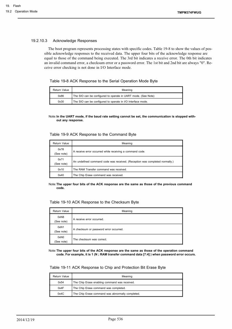
19.2.10.3 Acknowledge Responses
The boot program represents processing states with specific codes. Table 19-8 to show the values of pos-sible acknowledge responses to the received data. The upper four bits of the acknowledge response areequal to those of the command being executed. The 3rd bit indicates a receive error. The 0th bit indicatesan invalid command error, a checksum error or a password error. The 1st bit and 2nd bit are always "0". Re-ceive error checking is not done in I/O Interface mode.
Table 19-8 ACK Response to the Serial Operation Mode Byte
Return Value Meaning
0x86 The SIO can be configured to operate in UART mode. (See Note)
0x30 The SIO can be configured to operate in I/O Interface mode.
Note: In the UART mode, if the baud rate setting cannot be set, the communication is stopped with-out any response.
Table 19-9 ACK Response to the Command Byte
Return Value Meaning
0x?8(See note)
A receive error occurred while receiving a command code.
0x?1(See note)
An undefined command code was received. (Reception was completed normally.)
0x10 The RAM Transfer command was received.
0x40 The Chip Erase command was received.
Note:The upper four bits of the ACK response are the same as those of the previous commandcode.
Table 19-10 ACK Response to the Checksum Byte
Return Value Meaning
0xN8(See note)
A receive error occurred.
0xN1(See note)
A checksum or password error occurred.
0xN0(See note)
The checksum was correct.
Note:The upper four bits of the ACK response are the same as those of the operation commandcode. For example, it is 1 (N ; RAM transfer command data [7:4] ) when password error occurs.
Table 19-11 ACK Response to Chip and Protection Bit Erase Byte
Return Value Meaning
0x54 The Chip Erase enabling command was received.
0x4F The Chip Erase command was completed.
0x4C The Chip Erase command was abnormally completed.
TMPM374FWUG
19. Flash
19.2 Operation Mode
Page 5362014/12/19

19.2.10.4 Determination of a Serial Operation Mode
The first byte from the controller determines the serial operation mode. To use UART mode for commu-nications between the controller and the target board, the controller must firstly send a value of 0x86 at adesired baud rate to the target board. To use I/O Interface mode, the controller must send a value of 0x30at 1/16 of the desired baud rate. Figure 19-4 shows the waveforms for the first byte in each mode.
Note:Between each point of A/B/C/D of Figure 19-4 is expressed as tAB, tAC, tAD, and tCD.
UART (0x86)
tAB
Point AStart bit 0 bit 1 bit 2 bit 3 bit 4 bit 5 bit 6 bit 7 Stop
Point B Point C Point D
tCD
I/O Interface(0x30)
tAB
Point Abit 0 bit 1 bit 2 bit 3 bit 4 bit 5 bit 6 bit 7
Point B Point C Point D
tCD
Figure 19-4 Serial Operation Mode Byte
After RESET is released, the boot program monitors the first serial byte from the controller, with theSIO reception disabled, and calculates the intervals of tAB, tAC and tAD. Figure 19-5 shows a flowchartdescribing the steps to determine the intervals of tAB, tAC and tAD. As shown in the flowchart, the bootprogram captures timer counts when each time the logic transition occurs in the first serial byte. Consequent-ly, the calculated tAB, tAC and tAD intervals tend to have slight errors. If the transfer goes at a highbaud rate, the CPU might not be able to keep up with the speed of logic transitions at the serial receivepin. In particular, I/O Interface mode may have this problem since its baud rate is generally much higherthan that for UART mode. To avoid such a situation, the controller should send the first serial byte at1/16 of the desired baud rate.
The flowchart in Figure 19-5 shows how the boot program distinguishes between UART and I/O Inter-face modes. If the length of tAB is equal to or less than the length of tCD, the serial operation mode is de-termined as UART mode. If the length of tAB is greater than the length of tCD, the serial operationmode is determined as I/O Interface mode. Note that if the baud rate is too high or the timer operating fre-quency is too low, each timer value becomes small. It causes an unintentional behavior of the controller.To prevent this problem, reset UART mode within the programming routine.
For example, the serial operation mode may be determined to be I/O Interface mode when the intendedmode is UART mode. To avoid such a situation, when UART mode is utilized, the controller should al-low for a time-out period within which it expects to receive an echo-back (0x86) from the target board.The controller should give up the communication if it fails to get that echo-back within the allowed time.When I/O Interface mode is utilized, once the first serial byte has been transmitted, the controller shouldsend the SCLK clock after a certain idle time to get an acknowledge response. If the received acknowl-edge response is not 0x30, the controller should give up further communications.
When the intended mode is I/O interface mode, the first byte does not have to be 0x30 as long as tABis greater than tCD as shown above. 0x91, 0xA1 or 0xB1 can be sent as the first byte code to determinethe falling edges of Point A and Point C and the rising edges of Point B and Point D. If tAB is greaterthan tCD and SIO is selected by the resolution of the operation mode determination, the second bytecode is 0x30 even though the transmitted code on the first byte is not 0x30 (The first byte code to deter-mine I/O interface mode is described as 0x30).
TMPM374FWUG
Page 537 2014/12/19

Start
Initialize TMRB0Prescaler is on.(source clock:φT0)
High-to-low transitionon serial receive pin ?
TMRB0 starts counting up
Low-to-high transitionon serial receive pin ?
Software-capture and save timer value (tAB)
YES
YES
High-to-low transitionon serial receive pin ?
Software-capture and save timer value (tAC)
YES
Low-to-high transitionon serial receive pin ?
Software-capture and save timer value (tAD)
YES
16-bit Timer 0 stops countting
AC tAD?
Make backup copy of tAD value
Point A
Point B
Point C
Point D
Done Stop operation(infinite wating for RESET)
YES
Figure 19-5 Serial Operation Mode Byte Reception Flowchart
TMPM374FWUG
19. Flash
19.2 Operation Mode
Page 5382014/12/19

Start
tCD← tAD tAC
AB > tCD?
UART mode
YES
I/O interface mode
Figure 19-6 Serial Operation Mode Determination Flowchart
19.2.10.5 Password
The RAM Transfer command (0x10) causes the boot program to perform password verification. Follow-ing an echo-back of the command code, the boot program verifies the contents of the 12-byte passwordarea within the flash memory. The following table shows the password area of each product.
Product name Area
TMPM374FWUG 0x3F81_FFF4 to 0x3F81_FFFF
Note: If a password is set to 0xFF (erased data area), it is difficult to protect data securely due toan easy-to-guess password. Even if Single Boot mode is not used, it is recommended to seta unique value as a password.
If all these address locations contain the same bytes of data other than 0xFF, a password area error oc-curs as shown in Figure 19-7. In this case, the boot program returns an error acknowledge (0x11) in re-sponse to the checksum byte (the 17th byte), regardless of whether the password sequence sent from the con-troller is all 0xFFs.
Receiving data (5th to 16th bytes) from the controller is compared to the password stored in the flashmemory. All of the 12 bytes must match to pass the password verification. Otherwise, a password error oc-curs, which causes the boot program to reply an error acknowledge in response to the checksum byte (the17th byte).
The password verification is performed even if the security function is enabled.
Start
Are all bytes the same ?
YESAre all bytesequal to 0xFF
Password area error Password area is normal.
YES
Figure 19-7 Password Area Verification Flowchart
TMPM374FWUG
Page 539 2014/12/19

19.2.10.6 Checksum Calculation
The checksum byte for a series of bytes of data is calculated by adding the bytes together with ignor-ing the carries and calculating the 8-bit two’s complement by using lower 8 bits. The controller must per-form the same checksum operation in transmitting checksum bytes.
Example) To calculate the checksum for a series of 0xE5 and 0xF6:
Add the bytes together
0xE5 + 0xF6 = 0x1DB
Calculate the two’s complement by using lower 8 bits, and that is the checksum byte. Then send 0x25to the controller.
0 - 0xDB = 0x25
TMPM374FWUG
19. Flash
19.2 Operation Mode
Page 5402014/12/19

19.2.11 General Boot Program Flowchart
Figure 19-8 shows an overall flowchart of the boot program.
Single Bootprogram starts
Initialize
Get SIO operation mode
SIO operationmode ?
Set I/O interface mode
ACK data ← received data(0x30@I/O interface)
(Send 0x30)Normal response
Prepare to get a command
ACK data ← ACK data & 0xF0
Receive routineGet a command
Receive error ?
RAM transfer ?
ACK data ← Received data (0x10)
Transmission roiutine(Send 0x10: normal response)
RAM transfer processing
No normally
YES (0x10)
Chip erase ?
ACK data← Received data (0x40)
Transmission roiutine(Send 0x40: normal response)
Chip erase processing
YES (0x40)
ACK data ← ACK data 0x08
Transmission routine(Send x8H: receive error)
Yes
ACK data← Received data (0x01)
Command error
Transmission routine(Send 0xX1: Command error)
Processednormally?
Jump to RAM
Yes normally
Baud ratesetting ?
Program UART mode andbaud rate
ACK data ← received data(0x86@UART)
(Send 0x86)Normal response
Stop operation
UART Can not be set
Figure 19-8 Overall Boot Program Flowchart
TMPM374FWUG
Page 541 2014/12/19

19.3 On-board Programming of Flash Memory (Rewrite/Erase)In on-board programming, the CPU is to execute software commands for rewriting or erasing the flash memo-
ry. The rewrite/erase control program should be prepared by the user beforehand. Because the flash memory con-tent cannot be read while it is being written or erased, it is necessary to run the rewrite/erase program from the in-ternal RAM after shifting to the user boot mode.
19.3.1 Flash Memory
Except for some functions, writing and erasing flash memory data are in accordance with the standard JE-DEC commands.
In writing or erasing, use 32-bit data transfer command of the CPU to enter commands to the flash memo-ry. Once the command is entered, the actual write or erase operation is automatically performed internally.
Table 19-12 Flash Memory Functions
Major functions Description
Automatic page program Writes data automatically per page.
Automatic chip erase Erase the entire area of the flash memory automatically.
Automatic block erase Erases a selected block automatically.
Protect function The write or erase operation can be individually inhibited for each block.
19.3.1.1 Block Configuration
(1) TMPM374FWUG
64K bytes (BLOCK0)
32K bytes (BLOCK1)
16K bytes (BLOCK3)
16K bytes (BLOCK2)
0x3F81_FFFF
0x3F81_0000
0x3F80_8000
0x3F80_4000
0x3F80_0000
Single Boot Mode
0x0001_FFFF
0x0001_0000
0x0000_8000
0x0000_4000
0x0000_0000
User Boot Mode Page Configuration
64 words 256
64 words 128
64 words 64
64 words 64
Figure 19-9 Block Configuration of Flash Memory (TMPM374FWUG)
TMPM374FWUG
19. Flash
19.3 On-board Programming of Flash Memory (Rewrite/Erase)
Page 5422014/12/19

19.3.1.2 Basic Operation
This flash memory device has the following two operation modes:
・ The mode to read memory data (Read mode)・ The mode to automatically erase or rewrite memory data (Automatic operation)
Transition to the automatic mode is made by executing a command sequence while it is in the memoryread mode. In the automatic operation mode, flash memory data cannot be read and any commands stor-ed in the flash memory cannot be executed. In the automatic operation mode, any interrupt or exception gen-eration cannot set the device to the read mode except when a hardware reset is generated. During automat-ic operation, be sure not to cause any exception other than reset and debug exceptions while a debug portis connected. Any exception generation cannot set the device to the read mode except when a hardware re-set is generated.
(1) Read
When data is to be read, the flash memory must be set to the read mode. The flash memory willbe set to the read mode immediately after power is applied, when CPU reset is removed, or whenan automatic operation is normally terminated. In order to return to the read mode from othermodes or after an automatic operation has been abnormally terminated, either the Read/reset com-mand (a software command to be described later) or a hardware reset is used. The device must alsobe in the read mode when any command written on the flash memory is to be executed.
・ Read / reset command and Read command (software reset)
When ID-Read command is used, the reading operation is terminated instead of automat-ically returning to the read mode. In this case, the Read/reset command can be used to re-turn the flash memory to the read mode. Also, when a command that has not been complete-ly written has to be canceled, the Read/reset command must be used. The Read commandis used to return to the read mode after executing 32-bit data transfer command to writethe data "0x0000_00F0" to an arbitrary address of the flash memory.
・ With the Read/reset command, the device is returned to the read mode after completingthe third bus write cycle.
TMPM374FWUG
Page 543 2014/12/19

(2) Command write
This flash memory uses the command control method. Commands are executed by executing a com-mand sequence to the flash memory. The flash memory executes automatic operation commands ac-cording to the address and data combinations applied (refer to Command Sequence).
If it is desired to cancel a command write operation already in progress or when any incorrect com-mand sequence has been entered, the Read/reset command is to be executed. Then, the flash memo-ry will terminate the command execution and return to the read.
While commands are generally comprised of several bus cycles and the operation applying to the32-bit (word) data transmission command to the flash memory is called "bus write cycle". The buswrite cycles have a specific sequential order and the flash memory will perform an automatic opera-tion when the sequence of the bus write cycle data and address of command write is operated in accord-ance with a predefined specific order. If any bus write cycle does not follow a predefined commandwrite sequence, the flash memory will terminate the command execution and return to the read mode.
Note 1: Command sequences are executed from outside the flash memory area.Note 2: Each bus write cycle must be sequentially executed by 32-bit data transmit command.
While a command sequence is being executed, access to the flash memory is prohibi-ted. Also, do not generate any interrupt (except debug exceptions when a debug port isconnected). If such an operation is made, it may result in an unexpected read access tothe flash memory, and the command sequencer may not be able to correctly recognizethe command. While it may cause an abnormal termination of the command sequence,it also may cause an incorrect recognition of the command.
Note 3: For the command sequencer to recognize a command, the device must be in the readmode prior to executing the command. Be sure to check before the first bus write cyclewhere FCFLCS <RDY/BSY> is set to "1". It is recommended to subsequently execute aRead command.
Note 4: Upon issuing a command, if any address or data is incorrectly written, be sure to per-form a software reset to return to the read mode again.
19.3.1.3 Reset (Hardware reset)
A hardware reset is used to cancel the operational mode set by the command write operation when forci-bly terminated during auto programming/erasing or abnormal termination in the automatic operation.
The flash memory has a reset input as the memory block and it is connected to the CPU reset signal. There-fore, when the RESET input pin of this device is set to VIL or when the CPU is reset due to any over-flow of the watch dog timer, the flash memory will return to the read mode terminating any automatic op-eration that may be in progress. It should also be noted that applying a hardware reset during an automat-ic operation can result in incorrect rewriting of data. In such a case, be sure to perform the rewriting again.
Refer to Section "19.2.1 Reset Operation" for CPU reset operations. After a given reset input, the CPUwill read the reset vector data from the flash memory and starts operation after the reset is removed.
TMPM374FWUG
19. Flash
19.3 On-board Programming of Flash Memory (Rewrite/Erase)
Page 5442014/12/19

19.3.1.4 Commands
(1) Automatic Page Program
Writing to a flash memory device is to change "1" data cells to "0" data cells. Any "0" data cell can-not be changed to a "1" data cell. For changing "0" data cells to "1" data cells, it is necessary to per-form an erase operation.
The automatic page programming function of this device writes data of each page. TheTMPM374FWUG contains 64 words in a page. A 64 word block is defined by the same [31:8] ad-dress. It starts from the address [7:0] = 0x00 and ends at the address [7:0] = 0xFF. This program-ming unit is hereafter referred to as a "page".
Writing to data cells is automatically performed by an internal sequencer and no external controlby the CPU is required. The state of automatic page programming (whether it is in writing opera-tion or not) can be checked by FCFLCS [0] <RDY/BSY>.
Also, any new command sequence is not accepted while it is in the automatic page programmingmode. If it is desired to interrupt the automatic page programming, use the hardware reset function.If the operation is stopped by a hardware reset operation, it is necessary to once erase the page andthen perform the automatic page programming again because writing to the page has not been normal-ly terminated.
The automatic page programming operation is allowed only once for a page already erased. No pro-gramming can be performed twice or more. Note that rewriting to a page that has been once writtenrequires execution of the automatic block erase or automatic chip erase command before executingthe automatic page programming command again. Note that an attempt to rewrite a page two ormore times without erasing the content may cause damages to the device.
No automatic verify operation is performed internally to the device. So, be sure to read the data pro-grammed to confirm that it has been correctly written.
The automatic page programming operation starts when the third bus write cycle of the commandcycle is completed. After the fifth bus write cycle, data will be written sequentially starting fromthe next address of the address specified in the fourth bus write cycle (in the fourth bus write cycle,the page top address will be command written) (32 bits of data is input at one time). Be sure to usethe 32-bit data transfer command in writing commands after the fourth bus cycle. At this time, any32-bit data transfer commands shall not be placed across word boundary. After the fifth bus write cy-cle, data is command written to the same page area. Even if it is desired to write the page only parti-ally, it is required to perform the automatic page programming for the entire page. In this case, the ad-dress input for the fourth bus write cycle shall be set to the top address of the page. Be sure to per-form command write operation with the input data set to "1" for the data cells not to be set to "0".For example, if the top address of a page is not to be written, set the input data in the fourth buswrite cycle to 0xFFFFFFFF as a command write.
Once the third bus cycle is executed, the automatic page programming is in operation. This condi-tion can be checked by monitoring FCFLCS<RDY / BSY>. Any new command sequence is not accep-ted while it is in automatic page programming mode. If it is desired to stop operation, use the hard-ware reset function. Be careful in doing so because data cannot be written normally if the operationis interrupted. When a single page has been command written with normally terminating the automat-ic page writing process, FCFLCS<RDY / BSY> is set to "1" then it returns to the read mode.
When multiple pages are to be written, it is necessary to execute the page programming com-mand for each page because the number of pages to be written by a single execution of the automat-ic page program command is limited to only one page. It is not allowed for automatic page program-ming to process input data across pages.
Data cannot be written to a protected block. When automatic programming is finished, it automat-ically returns to the read mode. This condition can be checked by monitoring FCFLCS<RDY/
TMPM374FWUG
Page 545 2014/12/19

BSY>. If automatic programming has failed, the flash memory is locked in the current mode andwill not return to the read mode. For returning to the read mode, it is necessary to execute hardwarereset to reset the flash memory or the device. In this case, while writing to the address has failed, itis recommended not to use the device or not to use the block that includes the failed address.
Note:Software reset becomes ineffective after the fourth bus write cycle of the automaticpage programming command.
(2) Automatic chip erase
The automatic chip erase operation starts when the sixth bus write cycle of the command cycle iscompleted.
This condition can be checked by monitoring FCFLCS<RDY / BSY>. While no automatic verifyoperation is performed internally to the device, be sure to read the data to confirm that data hasbeen correctly erased. Any new command sequence is not accepted while it is in an automatic chiperase operation. If it is desired to stop operation, use the hardware reset function. If the operation isforced to stop, it is necessary to perform the automatic chip erase operation again because the data eras-ing operation has not been normally terminated.
Also, any protected block cannot be erased. If all the blocks are protected, the automatic chiperase operation will not be performed and it returns to the read mode after completing the sixth busread cycle of the command sequence. When an automatic chip erase operation is normally termina-ted, it automatically returns to the read mode. If an automatic chip erase operation has failed, theflash memory is locked in the current mode and will not return to the read mode.
For returning to the read mode, it is necessary to execute hardware reset to reset the device. Inthis case, the failed block cannot be detected. It is recommended not to use the device anymore orto identify the failed block by using the block erase function for not to use the identified block anymore.
(3) Automatic block erase (for each block)
The automatic block erase operation starts when the sixth bus write cycle of the command cycleis completed.
This status of the automatic block erase operation can be checked by monitoring FCFLCS<RDY / BSY>. While no automatic verify operation is performed internally to the device, be sureto read the data to confirm that data has been correctly erased. Any new command sequence is not ac-cepted while it is in an automatic block erase operation. If it is desired to stop operation, use the hard-ware reset function. In this case, it is necessary to perform the automatic block erase operationagain because the data erasing operation has not been normally terminated.
Also, any protected block cannot be erased. If an automatic block erase operation has failed, theflash memory is locked in the mode and will not return to the read mode. In this case, execute hard-ware reset to reset the device.
(4) Automatic programming of protection bits (for each block)
This device is implemented with protection bits. This protection can be set for each block. See Ta-ble 19-16 for table of protection bit addresses. This device assigns 1 bit to 1 block as a protectionbit. The applicable protection bit is specified by PBA in the seventh bus write cycle. By automatical-ly programming the protection bits, write and/or erase functions can be inhibited (for protection) indi-vidually for each block. The protection status of each block can be checked by FCFLCS <BLPRO>to be described later. This status of the automatic programming operation to set protection bits canbe checked by monitoring FCFLCS <RDY/BSY>. Any new command sequence is not acceptedwhile automatic programming is in progress to program the protection bits. If it is desired to stopthe programming operation, use the hardware reset function. In this case, it is necessary to performthe programming operation again because the protection bits may not have been correctly program-med. If all the protection bits have been programmed, all FCFLCS <BLPRO> are set to "1" indicat-ing that it is in the protected state. This disables subsequent writing and erasing of all blocks.
TMPM374FWUG
19. Flash
19.3 On-board Programming of Flash Memory (Rewrite/Erase)
Page 5462014/12/19

Note:Software reset is ineffective in the seventh bus write cycle of the automatic protectionbit programming command. FCFLCS <RDY/BSY> turns to "0" after entering the sev-enth bus write cycle.
(5) Automatic erasing of protection bits
Different results will be obtained when the automatic protection bit erase command is executed de-pending on the status of the protection bits and the security bits. It depends on whether all<BLPRO> in the FCFLCS register are set to "1" or not, when FCSECBIT<FCSECBIT> is set to"1". Be sure to check the value of FCFLCS <BLPRO> before executing the automatic protectionbit erase command. See Chapter "Protect/security function" for details.
・ When all the FCFLCS <BLPRO> are set to "1" (all the protection bits are programmed):
When the automatic protection bit erase command is command written, the flash memo-ry is automatically initialized within the device. When the seventh bus write cycle is comple-ted, the entire area of the flash memory data cells is erased and then the protection bits areerased. This operation can be checked by monitoring FCFLCS <RDY/BSY>. If the automat-ic operation to erase protection bits is normally terminated, FCFLCS will be set to"0x00000001". Since no automatic verify operation is performed internally to the device,be sure to read the data to confirm that it has been correctly erased. For returning to theread mode while the automatic operation after the seventh bus cycle is in progress, it is nec-essary to use the hardware reset to reset the device. If this is done, it is necessary to checkthe status of protection bits by FCFLCS <BLPRO> after retuning to the read mode and per-form either the automatic protection bit erase, automatic chip erase, or automatic blockerase operation, as required.
・ When FCFLCS <BLPRO> include "0" (not all the protection bits are programmed):
If the automatic protection bit is cleared to "0", the protection condition is canceled.With this device, protection bits can be programmed to an individual block and performedbit-erase operation in the four bits unit as shown in Table 19-16. The target bits are speci-fied in the seventh bus write cycle.The protection status of each block can be checked byFCFLCS <BLPRO> to be described later. This status of the programming operation for au-tomatic protection bits can be checked by monitoring FCFLCS <RDY/BSY>. When the au-tomatic operation to erase protection bits is normally terminated, the protection bits ofFCFLCS <BLPRO> selected for erasure are set to "0".
In any case, any new command sequence is not accepted while it is in an automatic operation toerase protection bits. If it is desired to stop the operation, use the hardware reset function. When theautomatic operation to erase protection bits is normally terminated, it returns to the read mode.
Note:The FCFLCS <RDY / BSY> bit is "0" while in automatic operation and it turns to "1"when the automatic operation is terminated.
(6) ID-Read
Using the ID-Read command, you can obtain the type and other information on the flash memorycontained in the device. The data to be loaded will be different depending on the address [15:14] ofthe fourth and subsequent bus write cycles (recommended input data is 0x00). After the fourth buswrite cycle, when an arbitrary flash memory area is read, the ID value will be loaded. Once thefourth bus write cycle of an ID-Read command has passed, the device will not automatically returnto the read mode. In this condition, the set of the fourth bus write cycle and ID-Read commandscan be repeatedly executed. For returning to the read mode, use the Read/reset command or hard-ware reset command.
TMPM374FWUG
Page 547 2014/12/19

19.3.1.5 Flash control / status register
Base Address = 0x41FF_F000
Register name Address (Base+)
Reserved - 0x0000
Reserved - 0x0004
Security bit register FCSECBIT 0x0010
Reserved - 0x0014
Flash control register FCFLCS 0x0020
Reserved - 0x0024 to 0x0FFF
Note:Do not access to the reserved address.
(1) FCFLCS (Flash control register)
31 30 29 28 27 26 25 24
bit symbol - - - - - - - -
After reset 0 0 0 0 0 0 0 0
23 22 21 20 19 18 17 16
bit symbol - - - - BLPRO3 BLPRO2 BLPRO1 BLPRO0
After reset 0 0 0 0 (Note 2) (Note 2) (Note 2) (Note 2)
15 14 13 12 11 10 9 8
bit symbol - - - - - - - -
After reset 0 0 0 0 0 0 0 0
7 6 5 4 3 2 1 0
bit symbol - - - - - - - RDY/BSY
After reset 0 0 0 0 0 0 0 1
Bit Bit Symbol Type Function
31 to 20 − R Read as 0.
19 to 16 BLPRO3 toBLPRO0
R Protection for Block 3 to 00: disabled1: enabledEach of the protection bits represents the protection status of the corresponding block. When a bit is set to"1", it indicates that the block corresponding to the bit is protected. When the block is protected, data can-not be written to it.
15 to 1 − R Read as 0.
0 RDY/BSY R Ready / Busy (Note 1)0:Auto operating1:Auto operation terminated.Ready/Busy flag bitThe RDY/BSY output is provided as a means to monitor the status of automatic operation. This bit is a func-tion bit for the CPU to monitor the function. When the flash memory is in automatic operation, it outputs"0" to indicate that it is busy. When the automatic operation is terminated, it returns to the ready state and out-puts "1" to accept the next command. If the automatic operation has failed, this bit maintains the "0" out-put. By applying a hardware reset, it returns to "1".
Note 1: This command must be issued in the ready state. Issuing the command in the busy state may disableboth correct command transmission and further command input. To exit from the condition, execute sys-tem reset. System reset requires at least 0.5 μs regardless of the system clock frequency. In this condi-tion, it takes approx. 2 ms to enable reading after reset.
Note 2: The value varies depending on protection applied.
TMPM374FWUG
19. Flash
19.3 On-board Programming of Flash Memory (Rewrite/Erase)
Page 5482014/12/19
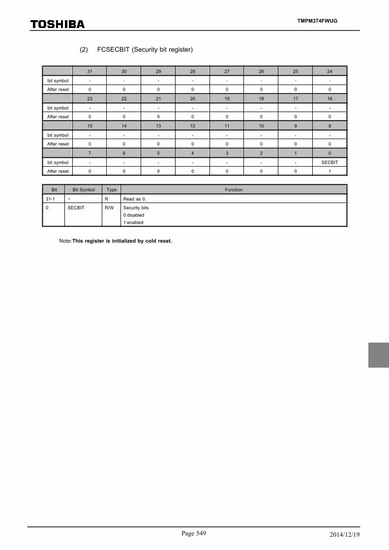
(2) FCSECBIT (Security bit register)
31 30 29 28 27 26 25 24
bit symbol - - - - - - - -
After reset 0 0 0 0 0 0 0 0
23 22 21 20 19 18 17 16
bit symbol - - - - - - - -
After reset 0 0 0 0 0 0 0 0
15 14 13 12 11 10 9 8
bit symbol - - - - - - - -
After reset 0 0 0 0 0 0 0 0
7 6 5 4 3 2 1 0
bit symbol - - - - - - - SECBIT
After reset 0 0 0 0 0 0 0 1
Bit Bit Symbol Type Function
31-1 − R Read as 0.
0 SECBIT R/W Security bits0:disabled1:enabled
Note:This register is initialized by cold reset.
TMPM374FWUG
Page 549 2014/12/19

19.3.1.6 List of Command Sequences
Table 19-13 shows the address and the data of each command of flash memory.
Bus cycles are "bus write cycles" except for the second bus cycle of the Read command, the fourth bus-cycle of the Read/reset command, and the fifth bus cycle of the ID-Read command. Bus write cycles are exe-cuted by 32-bit (word) data transfer commands. (In the following table, only lower 8 bits data are shown.)
See Table 19-14 for the detail of the address bit configuration. Use a value of "Addr." in the Table19-13 for the address [15:8] of the normal command in the Table 19-14.
Note:Always set "0" to the address bits [1:0] in the entire bus cycle.
Table 19-13 Flash Memory Access from the Internal CPU
Command sequence
First bus cy-cle
Second buscycle
Third bus cy-cle
Fourth buscycle
Fifth bus cy-cle
Sixth bus cy-cle
Seventh buscycle
Addr. Addr. Addr. Addr. Addr. Addr. Addr.
Data Data Data Data Data Data Data
Read0xXX − − − − − −
0xF0 − − − − − −
Read / Reset0x54XX 0xAAXX 0x54XX RA − − −
0xAA 0x55 0xF0 RD − − −
ID-Read0x54XX 0xAAXX 0x54XX IA 0xXX − −
0xAA 0x55 0x90 0x00 ID − −
Automatic page pro-gramming
0x54XX 0xAAXX 0x54XX PA PA PA PA
0xAA 0x55 0xA0 PD0 PD1 PD2 PD3
Automatic chip erase0x54XX 0xAAXX 0x54XX 0x54XX 0xAAXX 0x54XX −
0xAA 0x55 0x80 0xAA 0x55 0x10 −
Auto block erase0x54XX 0xAAXX 0x54XX 0x54XX 0xAAXX BA −
0xAA 0x55 0x80 0xAA 0x55 0x30 −
Protection bit program-ming
0x54XX 0xAAXX 0x54XX 0x54XX 0xAAXX 0x54XX PBA
0xAA 0x55 0x9A 0xAA 0x55 0x9A 0x9A
Protection bit erase0x54XX 0xAAXX 0x54XX 0x54XX 0xAAXX 0x54XX PBA
0xAA 0x55 0x6A 0xAA 0x55 0x6A 0x6A
Supplementary explanation
・ RA: Read address・ RD: Read data・ IA: ID address・ ID: ID data・ PA: Program page address
PD: Program data (32 bit data)
After fourth bus cycle, enter data in the order of the address for a page.・ BA: Block address・ PBA: Protection bit address
TMPM374FWUG
19. Flash
19.3 On-board Programming of Flash Memory (Rewrite/Erase)
Page 5502014/12/19

19.3.2 Address bit configuration for bus write cycles
Table 19-14 is used in conjunction with "Table 19-13 Flash Memory Access from the Internal CPU".
Address setting can be performed according to the normal bus write cycle address configuration from thefirst bus cycle. "0" is recommended" in the Table 19-14 Address Bit Configuration for Bus Write Cycles canbe changed as necessary.
AddressAddr
[31:19]Addr[18]
Addr[17]
Addr[16]
Addr[15]
Addr[14]
Addr[13:11]
Addr[10]
Addr[9]
Addr[8]
Addr[7:0]
Normalcommands
Normal bus write cycle address configuration
Flash area "0" is recommended. CommandAddr[1:0]="0" (fixed)
Others:0(recommended)
ID-READIA: ID address (Set the fourth bus write cycle address for ID-Read operation)
Flash area "0" is recommended. ID address Addr[1:0]="0" (fixed), Others:0 (recommended)
Block eraseBA: Block address (Set the sixth bus write cycle address for block erase operation)
Block selection (Table 19-14) Addr[1:0]="0" (fixed), Others:0 (recommended)
Auto pageprogram-ming
PA: Program page address (Set the fourth bus write cycle address for page programming operation)
Page selectionAddr[1:0]="0" (fixed)
Others:0 (recommended)
Protectionbit pro-gramming
PBA: Protection bit address (Set the seventh bus write cycle address for protection bit programming)
Flash areaProtection bit
selection(Table 19-15)
Fixed to "0".Protect bit se-
lection(Table 19-15)
Addr[1:0]="0" (fixed)Others:0 (recom-
mended)
Protectionbit erase
PBA: Protection bit address (Set the seventh bus erase cycle address for protection bit erasure)
Flash areaProtection bit
selection(Table 19-16)
Fixed to "0".Addr[1:0]="0" (fixed)
Others:0 (recommended)
As block address, specify any address in the block to be erased.
Refer to 19.3.1.1 for Block Configuration.
Table 19-14 Block Address Table
BlockAddress
(User boot mode)Address
(Single boot mode)Size
(Kbyte)
2 0x0000_0000 to 0x0000_3FFF 0x3F80_0000 to 0x3F80_3FFF 16
3 0x0000_4000 to 0x0000_7FFF 0x3F80_4000 o 0x3F80_7FFF 16
1 0x0000_8000 to 0x0000_FFFF 0x3F80_8000 to 0x3F80_FFFF 32
0 0x0001_0000 to 0x0001_FFFF 0x3F81_0000 to 0x3F81_FFFF 64
Note:As for the addresses from the first to the fifth bus cycles, specify the upper addresses of theblocks to be erased.
TMPM374FWUG
Page 551 2014/12/19

Table 19-15 Protection Bit Programming Address Table
Block Protection bit
The seventh bus write cycle address
Address[18]
Address[17]
Address[16]
Address[15:11]
Address[10]
Address[9]
Address[9]
Block0 <BLPRO[0]> 0 0
Fixed to "0".
0 0
Block1 <BLPRO[1]> 0 0 0 1
Block2 <BLPRO[2]> 0 0 1 0
Block3 <BLPRO[3]> 0 0 1 1
Table 19-16 Protection Bit Erase Address Table
Block Protection bit
The seventh bus write cycle address[18:17]
Address [18] Address [17]
Block0 to 3 <BLPRO[3:0]> 0 0
Block4 to 5 <BLPRO[5:4]> 0 1
Note:The protection bit erase command cannot erase by individual block.
Table 19-17 The ID-Read command's fourth bus write cycle ID address (IA) andthe data to be read by the following 32-bit data transfer command (ID)
IA[15:14] ID[7:0] Code
0y00 0x98 Manufacturer code
0y01 0x5A Device code
0y10 Reserved −
0y11 0x11 Macro code
TMPM374FWUG
19. Flash
19.3 On-board Programming of Flash Memory (Rewrite/Erase)
Page 5522014/12/19

19.3.2.1 Flowchart
Start
Automatic page programming command suquence(see the flowchart shown below)
The address of thelast page ?
YES
Automatic page programming
Address = Address + 0x200(set by a page)
NO
Automatic Page Programming Command Sequence (Address / Command)
0x54xx/0xAA
0xAAxx/0x55
0x54xx/0xA0
Programming address (page address)/Programming data (32 bit data)
Figure 19-10 Automatic Programming
Note:Command sequence is executed by 0x54xx or 0x55xx.
TMPM374FWUG
Page 553 2014/12/19

Start
Automatic chip erase command sequence(see the flowchart shown below)
Automatic chip erase completed
Automatic chip erase command sequence(address / command)
0x54xx/0xAA
0xAAxx/0x55
0x54xx/0x80
0x54xx/0xAA
0xAAxx/0x55
0x54xx/0x10
Automatic block / multi-block erase command sequence(address / command)
0x54xx/0xAA
0xAAxx/0x55
0x54xx/0x80
0x54xx/0xAA
0xAAxx/0x55
Block address/0x30
Figure 19-11 Automatic Erase
Note:Command sequence is executed by 0x54xx or 0x55xx.
TMPM374FWUG
19. Flash
19.3 On-board Programming of Flash Memory (Rewrite/Erase)
Page 5542014/12/19

20. ROM protection
20.1 OutlineThe TMPM374FWUG incorporates the write/erase protection function for the the internal ROM (flash) and the
security function which prevents reading the internal ROM (flash) area from the writer.
The protect/security function has the following two functions:
・ Write/erase protect for the internal ROM (flash)・ Security function
20.2 Feature
20.2.1 Write/ erase-protection function
The write/ erase-protection function enables the internal flash to prohibit the writing and erasing operationfor each block.
To activate the function, write "1" to the corresponding bits to a block to protect. Writing "0" to the bits can-cels the protection.
The protection settings of the bits can be monitored by the FCFLCS <BLPRO[3:0]> bit. See the chapter"Flash" for programming details.
20.2.2 Security function
The security function restricts flash ROM data readout and debugging.
This function is available under the conditions shown below.
1. The FCSECBIT <SECBIT> bit is set to"1".
2. All the protection bits (the FCFLCS<BLPRO> bits) used for the write/erase-protection function areset to "1".
Note:The FCSECBIT <SECBIT> bit is set to "1" at a power-on reset right after power-on.
Table 20-1 shows details of the restrictions by the security function.
Table 20-1 Restrictions by the security function
Item Details
1) ROM data readout Data can be read from CPU.
2) Debug port Communication of JTAG/SW and trace are prohibited
3) Command for flash memoryWriting a command to the flash memory is prohibited.An attempt to erase the contents in the bits used for the write/erase-protection erases all the protection bits.
TMPM374FWUG
Page 555 2014/12/19

20.3 Register
Base Address = 0x41FF_F000
Register name Address(Base+)
Reserved - 0x0000,0x0004
Security bit register FCSECBIT 0x0010
Reserved - 0x0014
Flash control register FCFLCS 0x0020
Reserved - 0x0024 to 0x0FFF
Note:Access to the "Reserved" area is prohibited.
TMPM374FWUG
20. ROM protection
20.3 Register
Page 5562014/12/19

20.3.1 FCFLCS (Flash control register)
31 30 29 28 27 26 25 24
bit symbol - - - - - - - -
After reset 0 0 0 0 0 0 0 0
23 22 21 20 19 18 17 16
bit symbol - - - - BLPRO3 BLPRO2 BLPRO1 BLPRO0
After reset 0 0 0 0 (Note2) (Note2) (Note2) (Note2)
15 14 13 12 11 10 9 8
bit symbol - - - - - - - -
After reset 0 0 0 0 0 0 0 0
7 6 5 4 3 2 1 0
bit symbol - - - - - - - RDY/BSY
After reset 0 0 0 0 0 0 0 1
Bit Bit Symbol Type Function
31-20 − R Read as 0.
19-16 BLPRO53 toBLPRO0
R Protection for Block3 to 00: disabled1: enabledProtection status bitsEach of the protection bits represents the protection status of the corresponding block. When a bit is set to"1," it indicates that the block corresponding to the bit is protected. When the block is protected, data can-not be written to it.
17-1 − R Read as 0.
0 RDY/BSY R Ready/Busy (Note 1)0: Auto operating1:Auto operation terminatedReady/Busy flag bitThe RDY/BSY output is provided as a means to monitor the status of automatic operation. This bit is a func-tion bit for the CPU to monitor the function. When the flash memory is in automatic operation, it outputs"0" to indicate that it is busy. When the automatic operation is terminated, it returns to the ready state and out-puts "1" to accept the next command. If the automatic operation has failed, this bit maintains the "0" out-put. By applying a hardware reset, it returns to "1."
Note 1: This command must be issued in the ready state. Issuing the command in the busy state may disable both cor-rect command transmission and further command input. To exit from the condition, execute system reset. Sys-tem reset requires at least 0.5 ms regardless of the system clock frequency. In this condition, it takes approx. 2ms to enable reading after reset.
Note 2: The value varies depending on protection applied.
TMPM374FWUG
Page 557 2014/12/19

20.3.2 FCSECBIT(Security bit register)
31 30 29 28 27 26 25 24
bit symbol - - - - - - - -
After reset 0 0 0 0 0 0 0 0
23 22 21 20 19 18 17 16
bit symbol - - - - - - - -
After reset 0 0 0 0 0 0 0 0
15 14 13 12 11 10 9 8
bit symbol - - - - - - - -
After reset 0 0 0 0 0 0 0 0
7 6 5 4 3 2 1 0
bit symbol - - - - - - - SECBIT
After reset 0 0 0 0 0 0 0 1
Bit Bit Symbol Type Function
31-1 − R Read as 0.
0 SECBIT R/W Security bit0: Disabled1: Enabled
Note:This register is initialized by cold reset.
TMPM374FWUG
20. ROM protection
20.3 Register
Page 5582014/12/19

20.4 Writing and erasing
20.4.1 Protection bits
Writing or erasing the protection bit is executed using the command sequence. Writing to the protectionbit is performed on each block. Erasing the protection bit is performed on the units of Block0 to 3.
Note that when all protection bits of all blocks are set to "1" and the FCSECBIT<SECBIT> bit is "1", the se-curity function is enabled. If the protection bits are erased on this condition, security function is erased andall protect bits are erased. Therefore, it is necessary to set "0" first to the FCSECBIT<SECBIT> bit and thenerase the protect bit.
See the chapter "Flash" for details
20.4.2 Security bit
The FCSECBIT <SECBIT> bit that activates the security function is set to "1" at a power-on reset that oc-curs immediately after power-on.
The bit is rewritten by the following procedure.
1. Write the code 0xa74a9d23 to FCSECBIT register.
2. Write data within 16 clocks from the above.1.
Note:The above procedure is enabled only when using 32-bit data transfer command.
TMPM374FWUG
Page 559 2014/12/19

TMPM374FWUG
20. ROM protection
20.4 Writing and erasing
Page 5602014/12/19
21. Debug Interface
21.1 Specification OverviewThe TMPM374FWUG contains the Serial Wire JTAG Debug Port (SWJ-DP) unit for interfacing with the De-
bug interface and the Embedded Trace Macrocell™ (ETM) unit for trace output. Trace data is output to the dedica-ted pins (SWV) via the on-chip Trace Port Interface Unit (TPIU).For more informarion of SWJ-DP,ETM andTPIY , please refer to the "Cortex-M3 Technical Reference Manual" issued by ARM Limited.
21.2 Features of SWJ-DPSWJ-DP supports the two-pin Serial Wire Debug Port (SWDCK, SWDIO) and the JTAG Debug Port (TDI,
TDO, TMS, TCK).
21.3 Features of ETMETM supports trace output from SWV.
TMPM374FWUG
Page 561 2014/12/19

21.4 Pin FunctionsThe debug interface pins can also be used as general-purpose ports. The PB3 and PB4 are shared between the
JTAG debug port function and the serial wire debug port function. The PB5 is shared between the JTAG debugport function and the SWV trace output function.
Table 21-1 SWJ-DP, ETM function
SWJ-DP Name of JTAG debug function SW debug
Pin name port I/O Description I/O Description
TMS/SWDIO PB3 InputJTAG Test Mode
SelectionI/O
Serial Wire DataInput/Output
TCK/SWCLK PB4 Input JTAG Test Check Input Serial Wire Clock
TDO/SWV PB5 Output JTAG Test Data Output(Input)(Note1)
(Serial Wire ViewerOutput)
TDI PB6 Input JTAG Test Data Input - -
Note:In case of enabling SWV function
After reset, the PB3, PB4, PB5 and PB6 are configured as debug port function pins. The functions of other de-bug interface pins need to be programmed as required. Debug interface pins can use general purpose port that isnot use debug interface.
Table 21-2 below summarizes the debug interface pin functions and related port settings after reset.
Table 21-2 Debug interface pins and port setting after reset
Initial Port Debug Port Setting After Reset (-;No register)
Setting (Bit name) FunctionFunction(PBFR)
Input(PBIE)
Output(PBCR)
OpenDrain
(PBOD)
Pull-up(PBPUP)
Pull-down
(PBPDN)
DEBUG PB3 TMS/SWDIO 1 1 1 0 1 0
DEBUG PB4 TCK/SWCLK 1 1 0 0 0 1
DEBUG PB5 TDO/SWV 1 0 1 0 0 0
DEBUG PB6 TDI 1 1 0 0 1 0
When using a low power consumption mode, take note of the following points.
Note 1: If PB3 and PB5 are configured as debug function pins, output continues to be enabled even in STOP mode re-gardless of the setting of the CGSTBYCR<DRVE>.
Note 2: If PB4 is configured as a debug function pin, it prevents a low power consumption mode from being fully effec-tive. Configure PB4 to function as a general-purpose port if the debug function is not used.
TMPM374FWUG
21. Debug Interface
21.4 Pin Functions
Page 5622014/12/19
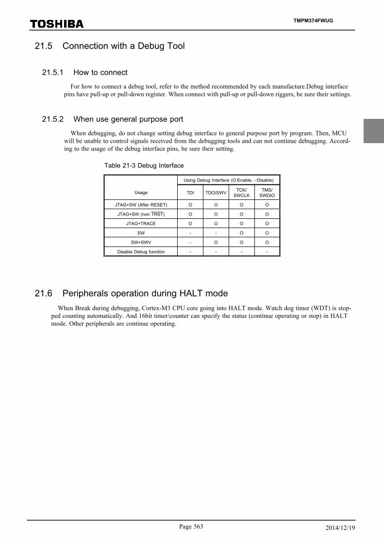
21.5 Connection with a Debug Tool
21.5.1 How to connect
For how to connect a debug tool, refer to the method recommended by each manufacture.Debug interfacepins have pull-up or pull-down register. When connect with pull-up or pull-down riggers, be sure their settings.
21.5.2 When use general purpose port
When debugging, do not change setting debug interface to general purpose port by program. Then, MCUwill be unable to control signals received from the debugging tools and can not continue debugging. Accord-ing to the usage of the debug interface pins, be sure their setting.
Table 21-3 Debug Interface
Using Debug Interface (Ο:Enable, -:Disable)
Usage TDI TDO/SWV TCK/SWCLK
TMS/SWDIO
JTAG+SW (After RESET) Ο Ο Ο Ο
JTAG+SW (non TRST) Ο Ο Ο Ο
JTAG+TRACE Ο Ο Ο Ο
SW - - Ο Ο
SW+SWV - Ο Ο Ο
Disable Debug function - - - -
21.6 Peripherals operation during HALT modeWhen Break during debugging, Cortex-M3 CPU core going into HALT mode. Watch dog timer (WDT) is stop-
ped counting automatically. And 16bit timer/counter can specify the status (continue operating or stop) in HALTmode. Other peripherals are continue operating.
TMPM374FWUG
Page 563 2014/12/19

TMPM374FWUG
21. Debug Interface
21.6 Peripherals operation during HALT mode
Page 5642014/12/19
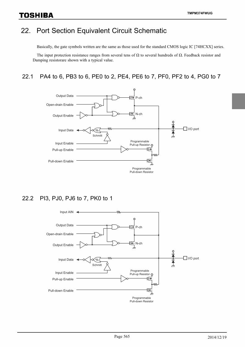
22. Port Section Equivalent Circuit Schematic
Basically, the gate symbols written are the same as those used for the standard CMOS logic IC [74HCXX] series.
The input protection resistance ranges from several tens of Ω to several hundreds of Ω. Feedback resistor andDamping resistorare shown with a typical value.
22.1 PA4 to 6, PB3 to 6, PE0 to 2, PE4, PE6 to 7, PF0, PF2 to 4, PG0 to 7
Output Data P-ch
Output Enable
Input Data
Input Enable
N-ch
I/O port
Open-drain Enable
Schmitt
ProgrammablePull-down Resistor
ProgrammablePull-up Resistor
Pull-down Enable
Pull-up Enable
22.2 PI3, PJ0, PJ6 to 7, PK0 to 1
Output Data P-ch
Output Enable
Input Data
Input Enable
N-ch
Open-drain Enable
Schmitt
Pull-down Enable
Pull-up Enable
Input AIN
I/O port
ProgrammablePull-down Resistor
ProgrammablePull-up Resistor
TMPM374FWUG
Page 565 2014/12/19

22.3 PM0 to 1
Output Data P-ch
Output Enable
Input Data
Input Enable
N-ch
Open-drain Enable
Schmitt
Pull-down Enable
Pull-up Enable
Input AIN
I/O port
ProgrammablePull-down Resistor
ProgrammablePull-up Resistor
22.4 X1, X2
X1
X21kΩ (typ.)
Oscillator Circuit
High-frequencyOscillation Enable
Clock
500kΩ(typ.)
22.5 RESET
Reset Input Port
Schmitt
Pull-up Resistor
TMPM374FWUG
22. Port Section Equivalent Circuit Schematic
22.3 PM0 to 1
Page 5662014/12/19

22.6 MODE
MODE Input Port
Schmitt
(Note)MODE pin is fixed to GND.
22.7 VREFHB, VREFLB
VREFH
VREFL
ADC
AVDD
AVSS
StringResistor
AVDD5(VREFH)
AVSS(VREFL)
22.8 VOUT15, VOUT3
VOUT15VOUT3 Output Pin
TMPM374FWUG
Page 567 2014/12/19

TMPM374FWUG
22. Port Section Equivalent Circuit Schematic
22.8 VOUT15, VOUT3
Page 5682014/12/19
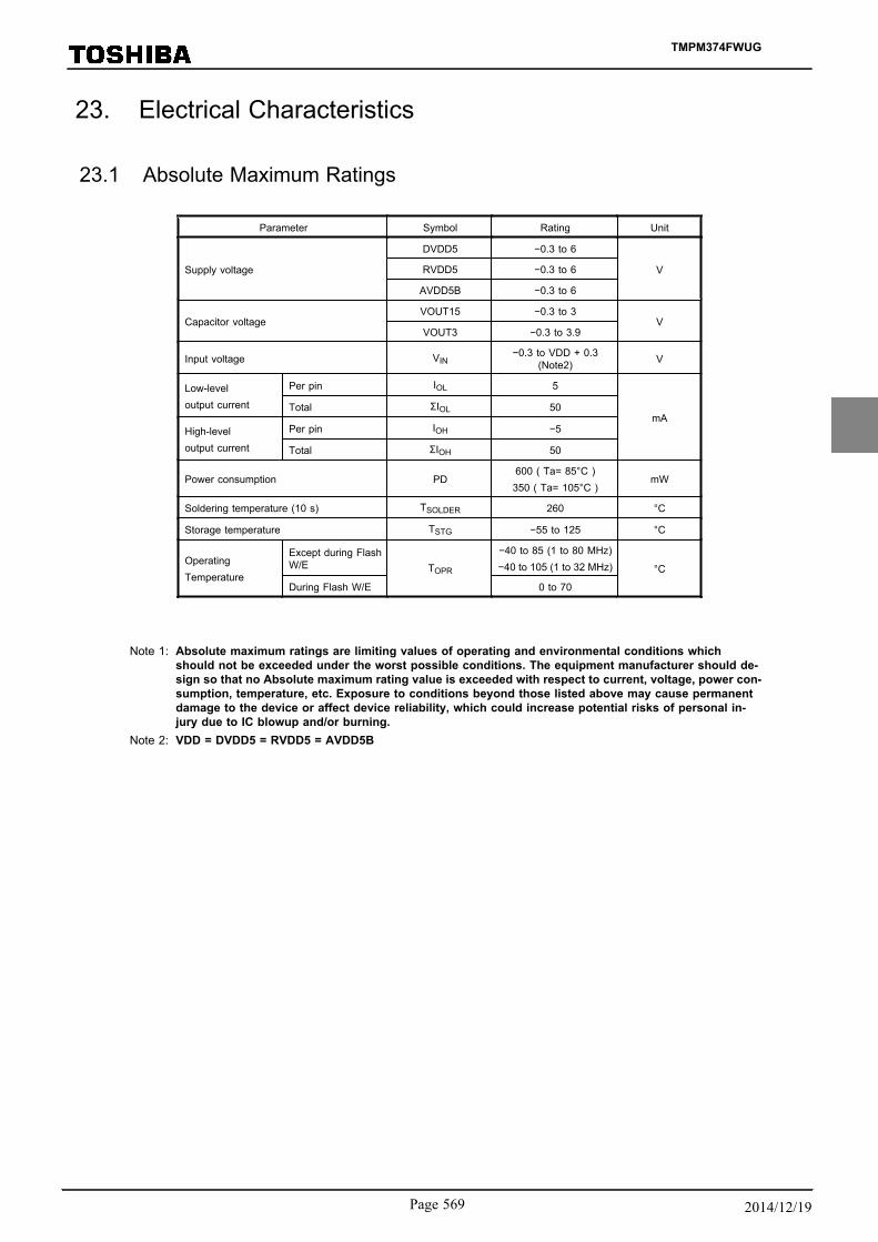
23. Electrical Characteristics
23.1 Absolute Maximum Ratings
Parameter Symbol Rating Unit
Supply voltage
DVDD5 −0.3 to 6
VRVDD5 −0.3 to 6
AVDD5B −0.3 to 6
Capacitor voltageVOUT15 −0.3 to 3
VVOUT3 −0.3 to 3.9
Input voltage VIN−0.3 to VDD + 0.3
(Note2) V
Low-leveloutput current
Per pin IOL 5
mATotal ΣIOL 50
High-leveloutput current
Per pin IOH −5
Total ΣIOH 50
Power consumption PD600 ( Ta= 85°C )
350 ( Ta= 105°C )mW
Soldering temperature (10 s) TSOLDER 260 °C
Storage temperature TSTG −55 to 125 °C
OperatingTemperature
Except during FlashW/E TOPR
−40 to 85 (1 to 80 MHz)−40 to 105 (1 to 32 MHz) °C
During Flash W/E 0 to 70
Note 1: Absolute maximum ratings are limiting values of operating and environmental conditions whichshould not be exceeded under the worst possible conditions. The equipment manufacturer should de-sign so that no Absolute maximum rating value is exceeded with respect to current, voltage, power con-sumption, temperature, etc. Exposure to conditions beyond those listed above may cause permanentdamage to the device or affect device reliability, which could increase potential risks of personal in-jury due to IC blowup and/or burning.
Note 2: VDD = DVDD5 = RVDD5 = AVDD5B
TMPM374FWUG
Page 569 2014/12/19

23.2 DC Electrical Characteristics (1/2)
DVSS = AVSSB = 0V, Ta = −40 to 105 °C
Parameter Symbol Rating Min. Typ. (Note 1) Max. Unit
Supplyvoltage(Note 2)
DVDD5RVDD5AVDD5B
VDDfOSC = 8 to 10 MHz
fsys = 1 to 80 MHz4.5 − 5.5 V
Supplyvoltage(duringFlash W/E)(Note 2)
DVDD5RVDD5AVDD5B
VDD
fOSC = 8 to 10 MHz
fsys = 1 to 80 MHz( Ta ( °C) = 0 to 70 )
4.5 − 5.5 V
Supplyvoltage(Power-on orPower-off)(Note 3)
DVDD5RVDD5AVDD5B
VDDfOSC = 8 to 10 MHz
fsys = 1 to 80 MHz3.9 − 5.5 V
Low-level inputvoltage Schmitt-Input VIL1 VDD = 4.5V to 5.5V (Note 4) −0.3
−0.25 VDD V
Hight-level in-put voltage Schmitt-Input VIH1 VDD = 4.5V to 5.5V (Note 4) 0.75VDD VDD V
Capacitance for VOUT15 andVOUT3 (Note 3)
CoutRVDD5 = 4.5V to 5.5VVOUT15, VOUT3
3.3 − 4.7 μF
Low-level output voltage VOL IOL = 1.6 mAVDD ≥ 4.5V(Note 4)
− − 0.4 V
High-level output voltage VOH IOH = −1.6 mAVDD ≥ 4.5V(Note 4)
4.1 − − V
Input leakage current ILI1 0.0 ≤ VIN ≤ VDD (Note 4) − 0.02 ±5μA
Output leakage current ILO 0.2 ≤ VIN ≤ VDD -0.2 (Note 4) − 0.05 ±10
Pull-up resister at Reset RRST 4.5 ≤ VDD ≤ 5.5 (Note 4) − 50 150 kΩ
Programmable pull-up/pull-down resistor PKH 4.5 ≤ VDD ≤ 5.5 (Note 4) − 50 150 kΩ
Schmitt-Triggered port VTH 4.5 ≤ VDD ≤ 5.5 (Note 4) 0.3 0.6 − μF
Pin capacitance(Except power supply pins)
CIO fc = 1 MHz − − 10 pF
Note 1: Ta = 25 °C, DVDD5 = AVDD5B = RVDD5 = 5V, unless otherwise noted.Note 2: The same voltage must be supplied to DVDD5, DVDD5B and RVDD5 .Note 3: It is a voltage range in the case of Power-on or Power-off (when VLTD disabled). In the range whose Power-line is
3.9V ≤ VDD < 4,5V, does not guarantee a 12-bit A/D converter and AC electrical Characteristics. Please refer to a ("Fig-ure 23-5 Powe on Sequence (Using Power On Reset only)") for details.
Note 4: VOUT15 and VOUT3 pin should be connected to GND via same value of capacitance. The IC outside can not havethe power supply from VOUT15 and VOUT3.
Note 5: VDD = DVDD5 = RVDD5 = AVDD5B
TMPM374FWUG
23. Electrical Characteristics
23.2 DC Electrical Characteristics (1/2)
Page 5702014/12/19

23.3 DC Electrical Characteristics (2/2)
DVDD5 =RVDD5 = AVDD5B = 4.5 V to 5.5 V, Ta = −40 to 85 °C
Parameter Symbol Rating Min.Typ.
(Note 1)Max. Unit
NORMAL (Note 2) Gear 1/1
IDDfsys = 80 MHz
− 43.5 59.5mA
IDLE (Note 4) Gear 1/1 − 15.5 25.5
STOP − − 3.5 7.5 mA
DVDD5 =RVDD5 = AVDD5B = 4.5 V to 5.5 V, Ta = −40 to 105 °C
Parameter Symbol Rating Min.Typ.
(Note 1)Max. Unit
NORMAL (Note 2) Gear 1/1
IDDfsys = 32 MHz
− 23.5 36.5mA
IDLE (Note 4) Gear 1/1 − 8.5 17.5
STOP − − 3.5 7.5 mA
Note 1: Ta=25°C, DVDD5= AVDD5B = RVDD5 = 5V, unless otherwise.Note 2: IDD NORMAL:
All functions operates excluding A/D.Note 3: A/D reference voltage supply can not go into off state.Note 4: IDD IDLE :
All peripheral functions stopped.
TMPM374FWUG
Page 571 2014/12/19

23.4 12-bit ADC Electrical Characteristics
DVDD5 = RVDD5 = AVDD5B / VREFHB = 4.5 V to 5.5 VDVSS = AVSSB / VREFLB = 0V, Ta = −40 to 105 °C
Parameter Symbol Rating Min. Typ. Max. Unit
Analog reference voltage (+)VREFHAVREFHB
− − AVDD − V
Analog input voltage VAIN − AVSS − AVDD V
Analog supply current(Note 1)
IREF DVSS = AVSS − 3.5 4.5 mA
Supply current A/D conversion − Except IREF − − 6.0 mA
INL error
−AIN resistance ≤ 600 ΩAIN load capacitance ≥ 0.1 μFConversion time ≥ 2 μs
− − ± 6
LSB
DNL error − − ± 5
Offset error − − ± 6
Full-scale error − − ± 6
Total error − − −10 to +6
Note 1: A/D reference voltage supply can not go into off state.Note 2: 1LSB = (AVDD − AVSS)/4096 [V]Note 3: AVDD = AVDD5B, AVSS = AVSSBNote 4: The characteristic is measured under the condition in which the only ADC is operating.
TMPM374FWUG
23. Electrical Characteristics
23.4 12-bit ADC Electrical Characteristics
Page 5722014/12/19

23.5 AC Electrical Characteristics
23.5.1 AC measurement condition
AC measurement condition
・ Output levels: High = 0.8 × VDD / Low = 0.2 × VDD・ Input levels: Refer to low-level input voltage and high-level input voltage in DC Electrical Character-
istics.・ Load capacity : CL = 30pF
Note:VDD = DVDD5 = AVDD5B
23.5.2 Serial Channel Timing (SIO/UART)
23.5.2.1 I/O Interface mode (VDD=4.5V to 5.5V)
In the table below, the letter x represents the period of the system clock (fsys). It varies depending onthe programming of the clock gear function.
(1) SCLK input mode (Ta = −40 to 85°C(1 to 80MHz) / Ta = −40 to 105°C(1 to32MHz))
[ Input ]
Parameter SymbolEquation 80 MHz
UnitMin. Max. Min. Max.
SCLK Clock High width (input) tSCH 3x − 37.5 −
ns
SCLK Clock Low width (input) tSCL 3x − 37.5 −
SCLK cycle tSCY tSCH + tSCL − 75 −
Input Data valid SCLK rise or fall(Note1)
tSRD 30 − 30 −
Input Data hold or fall afterSCLK rising (Note 1)
tHSR x + 30 − 42.5 −
[ Output ]
Parameter SymbolEquation 80 MHz
UnitMin. Max. Min. Max.
SCLK Clock High width (input) tSCH 3x −37.5
(Note 3)−
ns
SCLK Clock Low width (input) tSCL 3x −37.5
(Note 3)−
SCLK cycle tSCY tSCH + tSCL − 75 −
Output Data to SCLK rise or fall(Note 1)
tOSStSCY/2 − 3x− 45
(Note2)− 0 (Note 2) −
Input Data hold or fall afterSCLK rising (Note 1)
tOHS tSCY/2 − 37.5 −
Note 1: SCLK rise or fall: Measured relative to the programmed active edge of SCLK.Note 2: A calculated value should use it the SCLK cycle of the range which is not subtracted.Note 3: tOSS shows the minimum which is not subtracted.
TMPM374FWUG
Page 573 2014/12/19

(2) SCLK Output mode (Ta = −40 to 85°C(1 to 80MHz) / Ta = −40 to 105°C(1 to32MHz))
[ Output ]
Parameter SymbolEquation 80 MHz
UnitMin. Max. Min. Max.
SCK cycle (programmable) tSCY 4x − 60 −
ns
Output Data ← SCK rise tOSStSCY/2 − 30
(Note1)−
0(Note2)
−
SCK rise → Output Data hold tOHStSCY/2 − 30
(Note1)−
0(Note2)
−
Valid Data input ← SCK rise tSRD 45 − 45 −
SCK rise → Input Data hold tHSR 0 − 0 −
Note 1: A calculated value should use it the SCLK cycle of the range which is not subtracted.Note 2: tOSS shows the minimum which is not subtracted.
0 1 2 3
1
VALID
OUTPUT DATATxD
INPUT DATARxD
SCLK(Output mode/
Rising edge inputmode)
SCLK(Falling edge input
mode) tOSS
tSCY tSCHtSCL
tOHS
0
tSRD
2 3
tHSR
VALID VALIDVALID
Figure 23-1 Serial channel timing(SIO/UART)
TMPM374FWUG
23. Electrical Characteristics
23.5 AC Electrical Characteristics
Page 5742014/12/19
23.5.3 Event Counter
The character x shows the period of the clock for TMRB. The clock of TMRB is the same cycle as a sys-tem clock (fsys). It varies depending on the programming of the clock gear function.
Ta = −40 to 85°C (1 to 80MHz) / Ta = −40 to 105°C (1 to 32MHz)
Parameter SymbolEquation 80 MHz
UnitMin. Max. Min. Max.
Clock low pulse width tVCKL 2x + 100 − 125 − ns
Clock high pulse width tVCKH 2x + 100 − 125 − ns
23.5.4 Capture
The character x shows the period of the clock for TMRB. The clock of TMRB is the same cycle as a sys-tem clock (fsys). It varies depending on the programming of the clock gear function.
Ta = −40 to 85°C (1 to 80MHz) / Ta = −40 to 105°C (1 to 32MHz)
Parameter SymbolEquation 80 MHz
UnitMin. Max. Min. Max.
Low pulse width tCPL 2x + 100 − 125 − ns
High pulse width tCPH 2x + 100 − 125 − ns
23.5.5 External Interrupt
In the table below, the letter x represents the period of the system clock (fsys).
Ta= −40 to 85°C (1 to 80MHz)/Ta = −40 to 105°C (1 to 32MHz)
1. Except STOP release interrupts
Parameter SymbolEquation 80 MHz
Unit
Min. Max. Min. Max.
Low pulse width for INT0 to F tINTAL x + 100 − 112.5 − ns
High pulse width for INT0 to F tINTAH x + 100 − 112.5 − ns
2. STOP Release Interrupts
Parameter SymbolEquation
Unit
Min. Max. Min. Max.
Low pulse width for INT0 to F tINTBL 100 − 100 − ns
High pulse width for INT0 to F tINTBH 100 − 100 − ns
TMPM374FWUG
Page 575 2014/12/19

23.5.6 Debug Communication
23.5.6.1 AC measurement condition
・ Output levels : High = 0.7 × DVDD5, Low = 0.3 × DVDD5・ Load capacitance : CL(TRACECLK) = 25pF, CL(TRACEDATA) = 20pF
23.5.6.2 SWD Interface
Parameter Symbol Min. Max. Unit
CLK cycle Tdck 100 −
ns
DATA hold after CLK rising Td1 4 −
DATA valid after CLK rising Td2 − 37
DATA valid to CLK rising Tds 20 −
DATA hold after CLK falling Tdh 15 −
23.5.6.3 JTAG Interface
Parameter Symbol Min. Max. Unit
CLK cycle Tdck 100 −
ns
DATA hold after CLK falling Td3 4 −
DATA valid after CLK falling Td4 − 37
DATA valid to CLK rising Tds 20 −
DATA hold after CLK rising Tdh 15 −
Tdck
Td1
Td2
Td3
Td4
Tds Tdh
CLK input(SWCLK)(TCK)
Output data(SWDIO)
Output data(TDO)
Input data(SWDIO)(TMS/TDI)
Figure 23-2 JTAG and SWD communication timing
TMPM374FWUG
23. Electrical Characteristics
23.5 AC Electrical Characteristics
Page 5762014/12/19
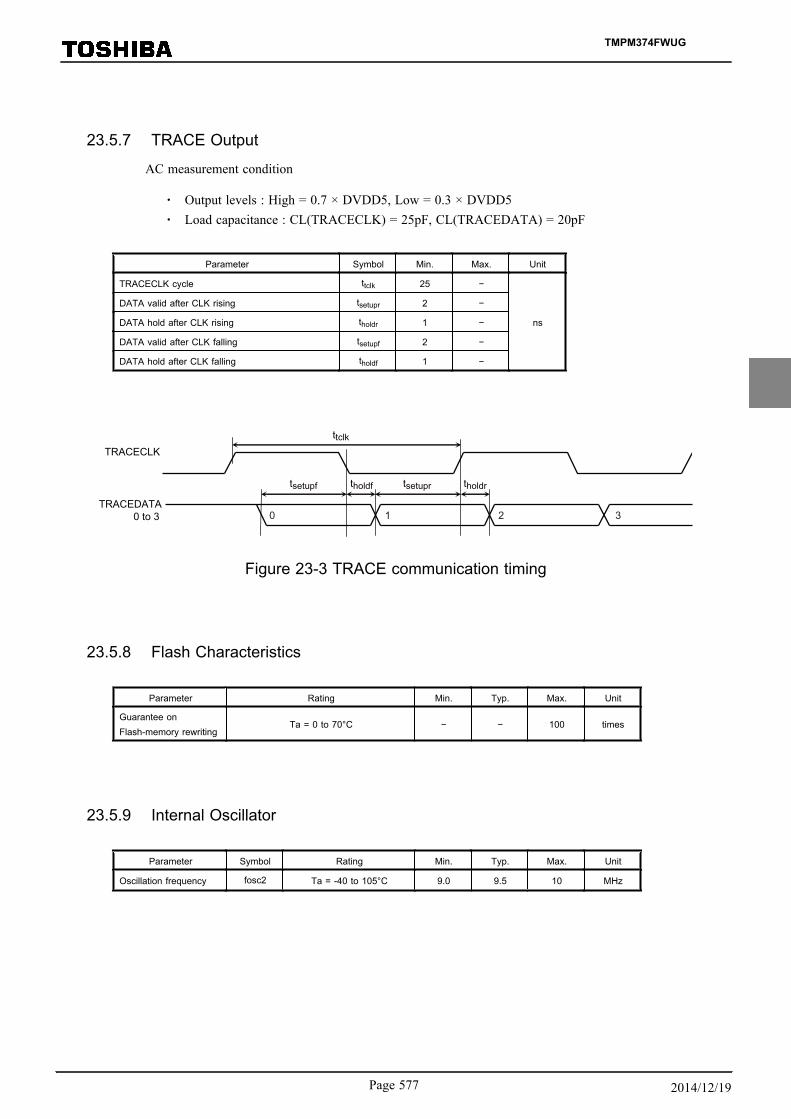
23.5.7 TRACE Output
AC measurement condition
・ Output levels : High = 0.7 × DVDD5, Low = 0.3 × DVDD5・ Load capacitance : CL(TRACECLK) = 25pF, CL(TRACEDATA) = 20pF
Parameter Symbol Min. Max. Unit
TRACECLK cycle ttclk 25 −
ns
DATA valid after CLK rising tsetupr 2 −
DATA hold after CLK rising tholdr 1 −
DATA valid after CLK falling tsetupf 2 −
DATA hold after CLK falling tholdf 1 −
0 1 2 3TRACEDATA 0 to 3
TRACECLK
tsetupf
ttclk
tholdf tsetupr tholdr
Figure 23-3 TRACE communication timing
23.5.8 Flash Characteristics
Parameter Rating Min. Typ. Max. Unit
Guarantee onFlash-memory rewriting
Ta = 0 to 70°C − − 100 times
23.5.9 Internal Oscillator
Parameter Symbol Rating Min. Typ. Max. Unit
Oscillation frequency fosc2 Ta = -40 to 105°C 9.0 9.5 10 MHz
TMPM374FWUG
Page 577 2014/12/19

23.6 Oscillation Circuit
X1 X2
C1 C2
Rd
Figure 23-4 High-frequency oscillation connection
Note 1: The load value of the oscillator is the sum of loads (C1 and C2) and the floating load of the actual assembled board.There is a possibility of operating error when using C1 and C2 values in the table below. When designing the board, de-sign the minimum length pattern around the oscillator. We also recommend that oscillator evaluation be carried out us-ing the actual board.
23.6.1 Recommended ceramic oscillator
The TX03 recommends the high-frequency oscillator by Murata Manufacturing Co., Ltd.
Please refer to the following URL for details.
http://www.murata.co.jp
TMPM374FWUG
23. Electrical Characteristics
23.6 Oscillation Circuit
Page 5782014/12/19

23.7 Notes on the power on
23.7.1 Using Power On Reset onlyNote 1: When you start a power supply using built-in power on reset, DVDD5 and RVDD5 terminal should start a power
supply to reach the recommendation operation voltage range (3.9 to 5.5V) within 215/fosc2.
Note 2: Please choose arbitrary disregard levels after the start of a microcomputer of operation in a voltage detector cir-cuit (VLTD), and enable operation.
Symbol Rating Min. Typ. Max. Unit
tPWUP Warming-up time after reset released - - 3.7ms
tDVDD Rising time of power line - - 3
VVLTDDetection voltage of a voltage detector circuit
(In the case of VDCR<VDLVL[1:0]> ="01")3.9 4.1 4.3
V
VPORH Power-on Reset releasing voltage 2.8 3 3.2
VPORL Power-on Reset detection voltage 2.6 2.8 3.0
Power-on counter
tDVDD
tPWUP
Reset state Normal mode Reset state
Please make a voltage detector circuit permission during
microcomputer operation.
note 3
note 4
Microcomputer operation
VPORH
0V
Power-on Reset Signal
Voltage detectorcircuit operation
(0 enable 1 deseble)
Supply voltage
Voltage detectioncercuit Reset
0.5V
VDD
VVLTD3.9V
VPORL
Figure 23-5 Powe on Sequence (Using Power On Reset only)
Note 1: VDD =DVDD5 = RVDD5 = AVDD5BNote 2: Since power-on-reset release voltage (VPORH) and power-on-reset detection voltage(VPORL) are changed relative-
ly, detection voltage does not reverse them.Note 3: If power supply voltage becomes VPORL or less, power on reset will start.
Note 4: A voltage detector circuit (VLTD) is initialized ( = VLTD is disable) by power-on-reset generating.
TMPM374FWUG
Page 579 2014/12/19

23.7.2 Using External Reset
23.7.2.1 IN case of the time of external reset shorter then POR
Power-on Counter
tDVDD
tPWUP
Depend on tPWUP
VPORH
0V
Power-on Reset Signal
RESET Signal
Supply voltage
Internal Reset Signal
0.5V
VDD
4.5V
Figure 23-6 Power on Sequence ( Using POR and External reset ) (1)
Note:VDD =DVDD5 = RVDD5 = AVDD5B
TMPM374FWUG
23. Electrical Characteristics
23.7 Notes on the power on
Page 5802014/12/19

23.7.2.2 IN case of the time of external reset longer then tPWUP
tDVDD
tPWUP
Depend on the time of external reset.
Power-on Counter
VPORH
0V
Internal Reset Signal
0.5V
VDD
4.5V
Supply voltage
Power-on Reset Signal
RESET Signal
Figure 23-7 Power on Sequence ( Using POR and External reset ) (2)
Note 1: VDD =DVDD5 = RVDD5 = AVDD5B
TMPM374FWUG
Page 581 2014/12/19

23.7.2.3 IN case of the rising time of power line longer then tPWUP
Power-on Counter
tDVDD
tPWUP
VDD must reach operating voltage and after 200μsec, external reset can released.
VPORH
0V
Power-on Reset Signal
RESET Signal
Supply voltage
Internal Reset Signal
0.5V
VDD
4.5V
Figure 23-8 Power on Sequence ( tDVDD > tPWUP )
Note 1: VDD =DVDD5 = RVDD5 = AVDD5BNote 2: In this case, must be reset from RESET pin.
TMPM374FWUG
23. Electrical Characteristics
23.7 Notes on the power on
Page 5822014/12/19
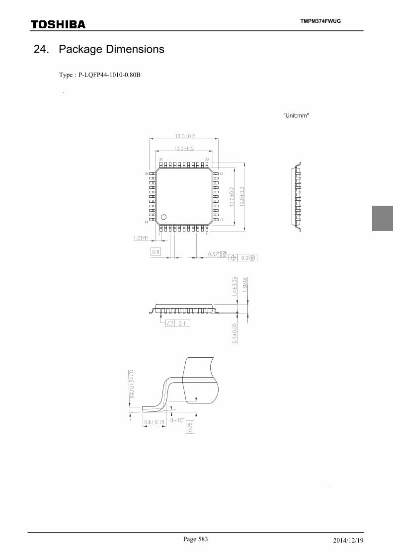
24. Package Dimensions
Type : P-LQFP44-1010-0.80B
TMPM374FWUG
Page 583 2014/12/19

TMPM374FWUG
24. Package Dimensions
Page 5842014/12/19

RESTRICTIONS ON PRODUCT USE• Toshiba Corporation, and its subsidiaries and affiliates (collectively "TOSHIBA"), reserve the right to make changes to the
information in this document, and related hardware, software and systems (collectively "Product") without notice.• This document and any information herein may not be reproduced without prior written permission from TOSHIBA. Even
with TOSHIBA's written permission, reproduction is permissible only if reproduction is without alteration/omission.• Though TOSHIBA works continually to improve Product's quality and reliability, Product can malfunction or fail. Customers
are responsible for complying with safety standards and for providing adequate designs and safeguards for their hardware, software and systems which minimize risk and avoid situations in which a malfunction or failure of Product could cause loss of human life, bodily injury or damage to property, including data loss or corruption. Before customers use the Product, create designs including the Product, or incorporate the Product into their own applications, customers must also refer to and comply with (a) the latest versions of all relevant TOSHIBA information, including without limitation, this document, the specifications, the data sheets and application notes for Product and the precautions and conditions set forth in the "TOSHIBA Semiconductor Reliability Handbook" and (b) the instructions for the application with which the Product will be used with or for. Customers are solely responsible for all aspects of their own product design or applications, including but not limited to (a) determining the appropriateness of the use of this Product in such design or applications; (b) evaluating and determining the applicability of any information contained in this document, or in charts, diagrams, programs, algorithms, sample application circuits, or any other referenced documents; and (c) validating all operating parameters for such designs and applications. TOSHIBA ASSUMES NO LIABILITY FOR CUSTOMERS' PRODUCT DESIGN OR APPLICATIONS.
• PRODUCT IS NEITHER INTENDED NOR WARRANTED FOR USE IN EQUIPMENTS OR SYSTEMS THAT REQUIRE EXTRAORDINARILY HIGH LEVELS OF QUALITY AND/OR RELIABILITY, AND/OR A MALFUNCTION OR FAILURE OF WHICH MAY CAUSE LOSS OF HUMAN LIFE, BODILY INJURY, SERIOUS PROPERTY DAMAGE AND/OR SERIOUS PUBLIC IMPACT ("UNINTENDED USE"). Except for specific applications as expressly stated in this document, Unintended Use includes, without limitation, equipment used in nuclear facilities, equipment used in the aerospace industry, medical equipment, equipment used for automobiles, trains, ships and other transportation, traffic signaling equipment, equipment used to control combustions or explosions, safety devices, elevators and escalators, devices related to electric power, and equipment used in finance-related fields. IF YOU USE PRODUCT FOR UNINTENDED USE, TOSHIBA ASSUMES NO LIABILITY FOR PRODUCT. For details, please contact your TOSHIBA sales representative.
• Do not disassemble, analyze, reverse-engineer, alter, modify, translate or copy Product, whether in whole or in part.• Product shall not be used for or incorporated into any products or systems whose manufacture, use, or sale is prohibited
under any applicable laws or regulations.• The information contained herein is presented only as guidance for Product use. No responsibility is assumed by TOSHIBA
for any infringement of patents or any other intellectual property rights of third parties that may result from the use of Product. No license to any intellectual property right is granted by this document, whether express or implied, by estoppel or otherwise.
• ABSENT A WRITTEN SIGNED AGREEMENT, EXCEPT AS PROVIDED IN THE RELEVANT TERMS AND CONDITIONS OF SALE FOR PRODUCT, AND TO THE MAXIMUM EXTENT ALLOWABLE BY LAW, TOSHIBA (1) ASSUMES NO LIABILITY WHATSOEVER, INCLUDING WITHOUT LIMITATION, INDIRECT, CONSEQUENTIAL, SPECIAL, OR INCIDENTAL DAMAGES OR LOSS, INCLUDING WITHOUT LIMITATION, LOSS OF PROFITS, LOSS OF OPPORTUNITIES, BUSINESS INTERRUPTION AND LOSS OF DATA, AND (2) DISCLAIMS ANY AND ALL EXPRESS OR IMPLIED WARRANTIES AND CONDITIONS RELATED TO SALE, USE OF PRODUCT, OR INFORMATION, INCLUDING WARRANTIES OR CONDITIONS OF MERCHANTABILITY, FITNESS FOR A PARTICULAR PURPOSE, ACCURACY OF INFORMATION, OR NONINFRINGEMENT.
• Do not use or otherwise make available Product or related software or technology for any military purposes, including without limitation, for the design, development, use, stockpiling or manufacturing of nuclear, chemical, or biological weapons or missile technology products (mass destruction weapons). Product and related software and technology may be controlled under the applicable export laws and regulations including, without limitation, the Japanese Foreign Exchange and Foreign Trade Law and the U.S. Export Administration Regulations. Export and re-export of Product or related software or technology are strictly prohibited except in compliance with all applicable export laws and regulations.
• Please contact your TOSHIBA sales representative for details as to environmental matters such as the RoHS compatibility of Product. Please use Product in compliance with all applicable laws and regulations that regulate the inclusion or use of controlled substances, including without limitation, the EU RoHS Directive. TOSHIBA ASSUMES NO LIABILITY FOR DAMAGES OR LOSSES OCCURRING AS A RESULT OF NONCOMPLIANCE WITH APPLICABLE LAWS AND
REGULATIONS.