AP431/AP431A Description Features Pin Assignments
18
AP431/AP431A Document number: DS31002 Rev. 21 - 2 1 of 17 www.diodes.com June 2013 © Diodes Incorporated AP431/AP431A ADJUSTABLE PRECISION SHUNT REGULATOR Description The AP431 and AP431A are 3-terminal adjustable precision shunt regulators with guaranteed temperature stability over the applicable extended commercial temperature range. The output voltage may be set at any level greater than 2.495V (V REF ) up to 36V merely by selecting two external resistors that act as a voltage divider network. These devices have a typical output impedance of 0.2Ω. Active output circuitry provides very sharp turn-on characteristics, making these devices excellent improved replacements for Zener diodes in many applications. The precise (+/-) 1% reference voltage tolerance of the AP431/AP431A make it possible in many applications to avoid the use of a variable resistor, consequently saving cost and eliminating drift and reliability problems associated with it. Features Precision Reference Voltage AP431: 2.495V ± 1% AP431A: 2.495V ± 0.5% Sink Current Capability: 200mA Minimum Cathode Current for Regulation: 300μA Equivalent Full-Range Temp Coefficient: 30ppm/°C Fast Turn-On Response Low Dynamic Output Impedance: 0.2Ω Programmable Output Voltage to 36V Low Output Noise Lead Free Packages: SOT25, SC59, SC59R, SOT89 SO-8 and TO92 Totally Lead-Free; RoHS Compliant (Notes 1 & 2) SOT23, SOT23R, SOT25, SC59, SC59R, SO-8, SOT89, TO92: Available in “Green” Molding Compound (No Br, Sb). See “Ordering Information” Halogen and Antimony Free. “Green” Device (Note 3) Pin Assignments (1) SOT25 (2) SO-8 4 REF 5 ANODE NC 1 CATHODE 3 NC 2 (Top View) NC 5 4 1 8 6 7 3 2 ANODE ANODE CATHODE NC ANODE REF ANODE (Top View) (3) SC59 (4) SC59R (5) SOT23 (6) SOT23R (Top View) ANODE 1 2 CATHODE 3 REF (7) SOT89 (8) TO92 1 2 3 Anode Cathode REF (Top View) (Top View) 1 REF 2 Anode + + + 3 Cathode Notes: 1. No purposely added lead. Fully EU Directive 2002/95/EC (RoHS) & 2011/65/EU (RoHS 2) compliant. 2. See http://www.diodes.com for more information about Diodes Incorporated’s definitions of Halogen- and Antimony-free, "Green" and Lead-free. 3. Halogen- and Antimony-free "Green” products are defined as those which contain <900ppm bromine, <900ppm chlorine (<1500ppm total Br + Cl) and <1000ppm antimony compounds.
-
Upload
khangminh22 -
Category
Documents
-
view
1 -
download
0
Transcript of AP431/AP431A Description Features Pin Assignments
AP431/AP431A Document number: DS31002 Rev. 21 - 2
1 of 17 www.diodes.com
June 2013© Diodes Incorporated
AP431/AP431A
ADJUSTABLE PRECISION SHUNT REGULATOR
Description
The AP431 and AP431A are 3-terminal adjustable precision shunt
regulators with guaranteed temperature stability over the applicable
extended commercial temperature range. The output voltage may be
set at any level greater than 2.495V (VREF) up to 36V merely by
selecting two external resistors that act as a voltage divider network.
These devices have a typical output impedance of 0.2Ω. Active output
circuitry provides very sharp turn-on characteristics, making these
devices excellent improved replacements for Zener diodes in many
applications.
The precise (+/-) 1% reference voltage tolerance of the
AP431/AP431A make it possible in many applications to avoid the
use of a variable resistor, consequently saving cost and eliminating
drift and reliability problems associated with it.
Features
Precision Reference Voltage
AP431: 2.495V ± 1%
AP431A: 2.495V ± 0.5%
Sink Current Capability: 200mA
Minimum Cathode Current for Regulation: 300μA
Equivalent Full-Range Temp Coefficient: 30ppm/°C
Fast Turn-On Response
Low Dynamic Output Impedance: 0.2Ω
Programmable Output Voltage to 36V
Low Output Noise
Lead Free Packages: SOT25, SC59, SC59R, SOT89 SO-8 and
TO92
Totally Lead-Free; RoHS Compliant (Notes 1 & 2)
SOT23, SOT23R, SOT25, SC59, SC59R, SO-8, SOT89, TO92:
Available in “Green” Molding Compound (No Br, Sb). See
“Ordering Information”
Halogen and Antimony Free. “Green” Device (Note 3)
Pin Assignments
(1) SOT25 (2) SO-8
4 REF
5 ANODENC 1
CATHODE 3
NC 2
(Top View)
NC 54
1 8
6
7
3
2
ANODE
ANODE
CATHODE
NC
ANODE
REF
ANODE
(Top View)
(3) SC59 (4) SC59R
(5) SOT23 (6) SOT23R
(Top View)
ANODE
1
2
CATHODE
3
REF
(7) SOT89 (8) TO92
1 2 3
Anode CathodeREF
(Top View) (Top View)
1 REF
2 Anode
+
+
+
3 Cathode
Notes: 1. No purposely added lead. Fully EU Directive 2002/95/EC (RoHS) & 2011/65/EU (RoHS 2) compliant. 2. See http://www.diodes.com for more information about Diodes Incorporated’s definitions of Halogen- and Antimony-free, "Green" and Lead-free. 3. Halogen- and Antimony-free "Green” products are defined as those which contain <900ppm bromine, <900ppm chlorine (<1500ppm total Br + Cl) and <1000ppm antimony compounds.

AP431/AP431A Document number: DS31002 Rev. 21 - 2
2 of 17 www.diodes.com
June 2013© Diodes Incorporated
AP431/AP431A
Typical Applications Circuit
++R1
V = (1 + R1/ R2) V
Precision Regulator
OUT REF
VIN VOUT
COUTCIN
A 431P
R2
Symbol
Cathode (C)
REF (R)
Anode (A)
Functional Block Diagram
+
-
Ca
tho
de
(C)
VREF
REF (R)
Anode (A)

AP431/AP431A Document number: DS31002 Rev. 21 - 2
3 of 17 www.diodes.com
June 2013© Diodes Incorporated
AP431/AP431A
Absolute Maximum Ratings (@TA = +25°C, unless otherwise specified.)
Parameter Rating Unit
Cathode Voltage +36 V
Continuous Cathode Current -10 to +250 mA
Reference Input Current 10 mA
Operating Temperature -20 to +85 °C
Storage Temperature -65 to +150 °C
Power Dissipation (Notes 4, 5)
SOT23(R) 400 mW
SOT25 550 mW
SC59(R) 400 mW
SO-8 600 mW
SOT89 800 mW
TO92 780 mW
Notes: 4. TJ, max = +150°C. 5. Ratings apply to ambient temperature at +25°C.
Electrical Characteristics (@TA = +25°C, VDD = 3V; unless otherwise specified.)
Symbol Parameter Conditions Min Typ Max Units
VREF Reference voltage VKA = VREF,
IKA = 10mA (Figure 1)
AP431 AP431A
2.470 2.482
2.495 2.520 2.507
V
VDEV Deviation of reference input voltage over temperature (Note 5)
VKA = VREF, IKA = 10mA
TA = Full Range (Figure 1) — 8.0 20.0 mV
ΔVREF
ΔVKA Ratio of the change in reference voltage to the change in cathode voltage IKA = 10mA (Figure 2)
VKA = VREF to 10V — -1.4 -2.0 mV/V
VKA = 10V to 36V — -1 -2 mV/V
IREF Refernce input current R1 = 10KΩ, R2 = ∞ IKA = 10mA (Figure 2) — 1.4 3.5 µA
IREF Deviation of reference input current over temperature
R1 = 10KΩ, R2 = ∞ IKA = 10mA
TA = Full range (Figure 2) — 0.4 1.2 µA
IKA(MIN) Minimum cathode current for regulation VKA = VREF (Figure 1) — 0.19 0.50 mA
IKA(OFF) Off-state current VKA = 36V, VREF = 0V (Figure 3) — 0.1 1.0 µA
|ZKA| Dynamic output impedance (Note 7) VKA = VREF VKA = VREF
ΔIKA = 0.1mA to 15mA Frequency ≤ 1KHz (Figure 1)
— 0.2 0.5 Ω

AP431/AP431A Document number: DS31002 Rev. 21 - 2
4 of 17 www.diodes.com
June 2013© Diodes Incorporated
AP431/AP431A
Electrical Characteristics (cont.) (@TA = +25°C, VDD = 3V; unless otherwise specified.)
V = V - VDEV MAX MIN
VMAX
VMIN
T1 T2Temperature
Note: 6. Deviation of reference input voltage, VDEV, is defined as the maximum variation of the reference over the full temperature range.
The average temperature coefficient of the reference input voltage VREF is defined as:
12
6
REF
DEV
REF TT
10)C)(25V
V(
Vα
……………………..………..…………….. ( ) Cppm
Where:
T2 – T1 = full temperature change.
VREF can be positive or negative depending on whether the slope is positive or negative.
Note: 7. The dynamic output impedance, RZ, is defined as:
KA
KAKA I
VZ
When the device is programmed with two external resistors R1 and R2 (see Figure 2.), the dynamic output impedance of the overall
circuit, is defined as:
)R2
R1(1Z
i
vZ KA
'KA
≈
Test Conditions
Input
VREF
VKA
IKA
Figure. 1 Test Circuit for V = VKA REF
IN
R1
R2
Note: V = V (1 + R1/R2) + I xR1
Figure. 2 Test Circuit for V > V
KA REF REF
KA REF
VKA
IKA
VREF
IREF
IZ(OFF)
Figure. 3 Test Circuit for Off-State Current
IN
VKA

AP431/AP431A Document number: DS31002 Rev. 21 - 2
5 of 17 www.diodes.com
June 2013© Diodes Incorporated
AP431/AP431A
Typical Performace Characteristics
0.5 1.5 2.5-0.5-1CATHODE VOLTAGE (V)
Cathode Current vs. Cathode Voltage
CA
TH
OD
E C
UR
RE
NT
(mA
)
100
0
-100
V = V
T = 25 CKA REF
A
0.5 1 1.5 2 2.50-0.5-1CATHODE VOLTAGE (V)
Cathode Current ( A) vs. Cathode Voltage
CA
TH
OD
E C
UR
RE
NT
(A
)
600
400
200
0
-200
IKA(MIN)
V = V
T = 25 CKA REF
A
0 60 80-20-40FREE-AIR TEMPERATURE (C)
Reference Voltage vs. Free-Air Temperature
20 40
CA
TH
OD
E C
UR
RE
NT
(mA
)
250
2490
2480
2485
2495
R1 = 10kI = 10mAKA
25 50 75 100 1250-25-50FREE-AIR TEMPERATURE (V)
Reverence Input Current vs. Free Temperature
RE
FE
RE
NC
E IN
PU
T C
UR
RE
NT
(A
)
2
1.8
1.4
1.2
1
1.6
10 25 3050CATHODE VOLTAGE (V)
Change in Reference Voltage vs. Cathode Voltage
15 20
CH
AN
GE
in R
EF
ER
EN
CE
VO
LTA
GE
(m
V)
0
-6
-12
-10
-2
-4
-8
I = 10mA
T = 25 CKA
A

AP431/AP431A Document number: DS31002 Rev. 21 - 2
6 of 17 www.diodes.com
June 2013© Diodes Incorporated
AP431/AP431A
Typical Performance Characteristics (cont.)
0.5 1.5 2.5-0.5-1CATHODE VOLTAGE (V)
Cathode Current vs. Cathode Voltage
CA
TH
OD
E C
UR
RE
NT
(mA
)
100
0
-100
V = V
T = 25 CKA REF
A
0.5 1 1.5 2 2.50-0.5-1CATHODE VOLTAGE (V)
Cathode Current ( A) vs. Cathode Voltage
CA
TH
OD
E C
UR
RE
NT
(A
)
600
400
200
0
-200
IKA(MIN)
V = V
T = 25 CKA REF
A
0 60 80-20-40FREE-AIR TEMPERATURE (C)
Reference Voltage vs. Free-Air Temperature
20 40
CA
TH
OD
E C
UR
RE
NT
(mA
)
250
2490
2480
2485
2495
R1 = 10kI = 10mAKA
25 50 75 100 1250-25-50FREE-AIR TEMPERATURE (V)
Reverence Input Current vs. Free Temperature
RE
FE
RE
NC
E IN
PU
T C
UR
RE
NT
(A
)
2
1.8
1.4
1.2
1
1.6
10 25 3050CATHODE VOLTAGE (V)
Change in Reference Voltage vs. Cathode Voltage
15 20
CH
AN
GE
in R
EF
ER
EN
CE
VO
LTA
GE
(m
V)
0
-6
-12
-10
-2
-4
-8
I = 10mA
T = 25 CKA
A

AP431/AP431A Document number: DS31002 Rev. 21 - 2
7 of 17 www.diodes.com
June 2013© Diodes Incorporated
AP431/AP431A
Typical Performance Characteristics (cont.)
100K10K1K 1M 10Mf-FREQUENCY -Hz
Small-Signal Voltage Amplification vs. Frequency
I = 10mA
T = 25 CKA
A
A -
SM
AL
L S
IGN
AL
VO
LTA
GE
AM
PLI
FIC
AT
ION
(dB
)V
60
50
40
30
20
10
0
GND
Output
232
8.25K
15K
9 F+ +
-
-
IKA
Test Circuit for Voltage Amplification
100K10K1K 1M 10Mf-FREQUENCY -Hz
Reference Impedance vs. Frequency
I = 10mA
T = 25 CKA
A
ZK
A
RE
FE
RE
NC
E I
MP
ED
AN
CE
100
10
1
0
1K
50
Output
GND
IKA
Test Circuit for Reference Impedance

AP431/AP431A Document number: DS31002 Rev. 21 - 2
8 of 17 www.diodes.com
June 2013© Diodes Incorporated
AP431/AP431A
Typical Performance Characteristics (cont.)
-1 0 1 2 3 4 5 6 7t- TIME ( s)
Pulse Response
0
1
2
3
4
5
6
INP
UT
an
d O
UT
PU
T V
OLT
AG
E (
V)
T = 25°CA
Input
Output
220
50
Output
GND
Test Circuit for Pulse Response
PulseGeneratorf = 100kHz
Stable
StableB
A
C
D
T = 25 CA A V = V
BKA REF
V = 5V
C V = 10V
D V = 15V
KA
KA
KA
C - LOAD CAPACITANCE ( F)
Stability Boundary Conditions
L †
0.001 0.01 0.1 1 10
100
90
80
70
60
50
40
30
10
0
20I-
CA
TH
OD
E C
UR
RE
NT
(m
A)
KA
†The areas under the curves represent conditions that may cause
the device to oscilate. For curves B, C, and D, R2 and V+ were adjusted to establish the initial VKA and IKA conditions with CL = 0. VBATT and CL were then adjusted to determine the ranges of stability.
150
VBATTCL
IKA
Test Circuit for Curve A
+
-
VBATT
150R1 = 10K
R2
CL
IKA
+
-
Test Circuit for Curve B, C, and D

AP431/AP431A Document number: DS31002 Rev. 21 - 2
9 of 17 www.diodes.com
June 2013© Diodes Incorporated
AP431/AP431A
Application Examples
VIN
R1B
R2B
R1A
R2A
LED on when Low Limit < V < High Limit
Low Limit V (1 + R1B/R2B)
High
IN
REF Limit V (1 + R1A/R2A)
Fig. 4 Voltage Monitor
REF
Fig 5. Delay Timer
NOFF
R
+
VINDelay = RC x ln (V - VIN REF)
VIN
I = V /ROUT REF CL
Fig 6. Current Limiter or Current Source
RCLIOUT
VIN
I = V / ROUT REF S
Fig. 7 Constant-Current Sink
RS
VIN IOUT
V = (1 + R1/R2) x VOUT REF
Fig. 8 Higher-Current Shunt Regulator
VIN VOUT
R1
R2
VOUTVIN
PULSER1
R2
Limit (1 + R1/R2) x V REF
Fig. 9 Crow Bar
+
Low Limit V (1 + R1B/R2B) + V
High
REF BE
Limit V (1 + R1A/R2A)
Fig. 10 Over-Voltage/ Under-Voltage Protection Circuit
REF
Output ON whenLow Limit < V < High LimitIN
VIN
R1A
VBE
R1B
R2A R2B
Note: 12. Online application note, “Design Consideration with AP431 when used as a Comparator”
URL: http://www.diodes.com/_files/products_appnote_pdfs/AN78.pdf

AP431/AP431A Document number: DS31002 Rev. 21 - 2
10 of 17 www.diodes.com
June 2013© Diodes Incorporated
AP431/AP431A
Ordering Information
Part Number (Note 10)
Package Code Packaging 7”/13 Tape and Reel Ammo Box
Quantity Part Number Suffix
(Note 11) Quantity
Part Number Suffix
AP431(A)SAG-7 SA SOT23 3000/Tape & Reel -7 NA NA
AP431(A)SRG-7 SR SOT23R 3000/Tape & Reel -7 NA NA
AP431(A)QL-7 Q SOT25 3000/Tape & Reel -7 NA NA
AP431(A)QG-7 Q SOT25 3000/Tape & Reel -7 NA NA
AP431AWL-7 W SC59 3000/Tape & Reel -7 NA NA
AP431(A)WG-7 W SC59 3000/Tape & Reel -7 NA NA
AP431(A)RL-7 R SC59R 3000/Tape & Reel -7 NA NA
AP431(A)RG-7 R SC59R 3000/Tape & Reel -7 NA NA
AP431(A)G-13 SO-8 2500/Tape & Reel -13 NA NA
AP431(A)YL-13 Y SOT89 2500/Tape & Reel -13 NA NA
AP431(A)YG-13 Y SOT89 2500/Tape & Reel -13 NA NA
AP431(A)YG-13R Y SOT89 4000/Tape & Reel -13R NA NA
AP431(A)VL-A V TO92 NA NA 2000/Box NA
AP431(A)VG-A V TO92 NA NA 2000/Box NA
Notes: 8. SO-8, SOT23 and SOT23R are available in “Green” products only. 9. Ammo Box is for TO92 Spread Lead.
10. Suffix “A” denotes AP431A device. 11. Details of tape and reel options can be seen in document AP2007, which can be found on our website at
http://www.diodes.com/datasheets/ap02007.pdf
Package Lead-Free PackingReference Voltage
Tolerance
Blank : ±1% A : ±0.5%
SA : SOT23SR : SOT23RQ : SOT25W : SC59R : SC59RBlank : SO-8Y : SOT89V : TO92
L : Lead FreeG : Green (Note 8)
7 : Tape & Reel (Note 11) 13 : Tape & Reel (Note 11)13R : Tape & Reel (Note 11) A : Ammo Box (Note 9)
PbLead-Free
PbLead-Free
PbLead-Free
PbLead-Free
PbLead-Free
AP431 X XX X - X
AP431/AP431A Document number: DS31002 Rev. 21 - 2
11 of 17 www.diodes.com
June 2013© Diodes Incorporated
AP431/AP431A
Marking Information (1) SC59 and SC59R
1 2
3
XX Y W X
( Top View )
XX : Identification code
W : Week : A~Z : 1~26 week;
X : A~Z : Green
Y : Year 0~9
a~z : 27~52 week; z represents52 and 53 week
a~z : Lead Free (2) SOT23 and SOT23R
1 2
3
XX Y W X
( Top View )
XX : Identification code
W : Week : A~Z : 1~26 week;
X : A~Z : Green
Y : Year 0~9
a~z : 27~52 week; z represents52 and 53 week
(3) SOT25
1 2 3
5 74
XX Y W X
( Top View )
XX : Identification code
W : Week : A~Z : 1~26 week;
X : A~Z : Green
Y : Year 0~9
a~z : 27~52 week; z represents52 and 53 week
a~z : Lead Free
(4) SO-8
( Top View )
AP431XYY WW X X
Logo
Part Number
58
41
G : Green
AccuracyBlank : 2.495 + 1% A : 2.495 + 0.5%
WW : Week : 01~52; 52YY : Year : 08, 09,10~
X : Internal Coderepresents 52 and 53 week
AP431/AP431A Document number: DS31002 Rev. 21 - 2
12 of 17 www.diodes.com
June 2013© Diodes Incorporated
AP431/AP431A
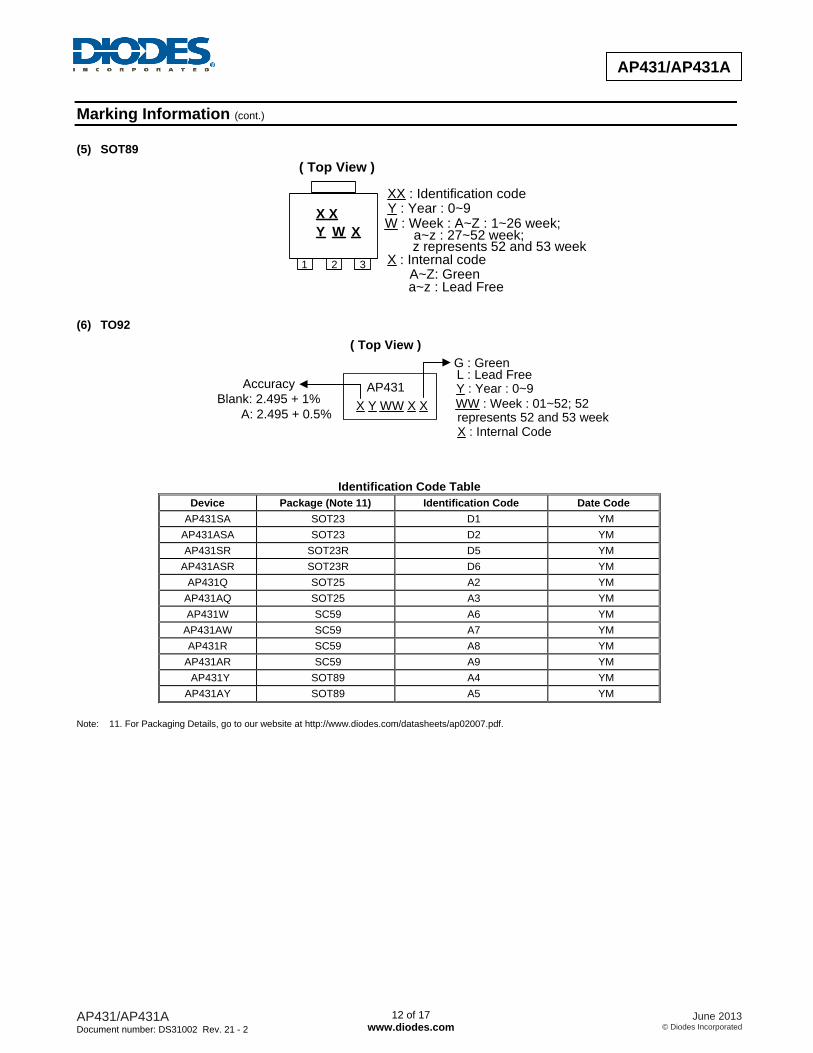
Marking Information (cont.)
(5) SOT89
1 32
X XY W
XX : Identification code
( Top View )
X
Y : Year : 0~9W : Week : A~Z : 1~26 week;
X : Internal code
a~z : 27~52 week;z represents 52 and 53 week
A~Z: Green a~z : Lead Free
(6) TO92
( Top View )
AP431
X Y WW X X
AccuracyBlank: 2.495 + 1%
A: 2.495 + 0.5%
G : Green
WW : Week : 01~52; 52Y : Year : 0~9
X : Internal Coderepresents 52 and 53 week
L : Lead Free
Identification Code Table Device Package (Note 11) Identification Code Date Code
AP431SA SOT23 D1 YM
AP431ASA SOT23 D2 YM
AP431SR SOT23R D5 YM
AP431ASR SOT23R D6 YM
AP431Q SOT25 A2 YM
AP431AQ SOT25 A3 YM
AP431W SC59 A6 YM
AP431AW SC59 A7 YM
AP431R SC59 A8 YM
AP431AR SC59 A9 YM
AP431Y SOT89 A4 YM
AP431AY SOT89 A5 YM
Note: 11. For Packaging Details, go to our website at http://www.diodes.com/datasheets/ap02007.pdf.

AP431/AP431A Document number: DS31002 Rev. 21 - 2
13 of 17 www.diodes.com
June 2013© Diodes Incorporated
AP431/AP431A
Package Outline Dimensions (All dimensions in mm.)
Please see AP02002 at http://www.diodes.com/datasheets/ap02002.pdf for latest version. (1) SOT25
(2) SO-8
(3) SC59 and SC59R
SOT25 Dim Min Max Typ
A 0.35 0.50 0.38 B 1.50 1.70 1.60 C 2.70 3.00 2.80 D 0.95 H 2.90 3.10 3.00 J 0.013 0.10 0.05 K 1.00 1.30 1.10 L 0.35 0.55 0.40 M 0.10 0.20 0.15 N 0.70 0.80 0.75 0° 8°
All Dimensions in mm
SO-8 Dim Min Max
A - 1.75 A1 0.10 0.20 A2 1.30 1.50 A3 0.15 0.25 b 0.3 0.5 D 4.85 4.95 E 5.90 6.10
E1 3.85 3.95 e 1.27 Typ h - 0.35 L 0.62 0.82 0 8
All Dimensions in mm
SC59 Dim Min Max Typ
A 0.35 0.50 0.38 B 1.50 1.70 1.60 C 2.70 3.00 2.80 D - - 0.95 G - - 1.90 H 2.90 3.10 3.00 J 0.013 0.10 0.05 K 1.00 1.30 1.10 L 0.35 0.55 0.40 M 0.10 0.20 0.15 N 0.70 0.80 0.75 0° 8° - All Dimensions in mm
A
M
JLD
B C
H
KN
Gauge PlaneSeating Plane
Detail ‘A’
Detail ‘A’
EE1
h
L
D
e b
A2
A1
A
45°7°~9°
A3
0.2
54
A
M
JLD
B C
H
K
G
N

AP431/AP431A Document number: DS31002 Rev. 21 - 2
14 of 17 www.diodes.com
June 2013© Diodes Incorporated
AP431/AP431A
Package Outline Dimensions (cont.) (All dimensions in mm.)
Please see AP02002 at http://www.diodes.com/datasheets/ap02002.pdf for latest version. (4) SOT23 and SOT23R
(5) SOT89
(6) TO92
SOT23 Dim Min Max Typ
A 0.37 0.51 0.40 B 1.20 1.40 1.30 C 2.30 2.50 2.40 D 0.89 1.03 0.915 F 0.45 0.60 0.535 G 1.78 2.05 1.83 H 2.80 3.00 2.90 J 0.013 0.10 0.05 K 0.903 1.10 1.00
K1 - - 0.400 L 0.45 0.61 0.55 M 0.085 0.18 0.11 0° 8° - All Dimensions in mm
SOT89 Dim Min Max
A 1.40 1.60 B 0.44 0.62
B1 0.35 0.54 C 0.35 0.44 D 4.40 4.60
D1 1.62 1.83 E 2.29 2.60 e 1.50 Typ H 3.94 4.25
H1 2.63 2.93 L 0.89 1.20
All Dimensions in mm
TO92 Dim Min Max Typ
A 3.45 3.66 — B 4.27 4.78 — b — — 0.38 c — — 0.38 D — — 3.87 E 4.32 4.83 — e — — 1.27
e2 2.40 2.90 — L 12.98 15.00 —
L1 12.80 15.00 — L2 0.80 — L3 2.00 3.00 — N 1.22 1.37 — All Dimensions in mm
A
M
J LD
F
B C
H
K
G
K1
EH
D1
B1 B
e
C
L
A
D
8° (4X)
H1
R0.200
EJECTION MARK
LOOSE PRODUCTTAPED PRODUCT
EJECTION MARK
B
E
b
ee
D
N
c e2 e2
L1
E
L2L3
A
L

AP431/AP431A Document number: DS31002 Rev. 21 - 2
15 of 17 www.diodes.com
June 2013© Diodes Incorporated
AP431/AP431A
Suggested Pad Layout Please see AP02001 at http://www.diodes.com/datasheets/ap02001.pdf for the latest version. (1) SOT25
(2) SO-8
(3) SC59 and SC59R
Dimensions Value (in mm) Z 3.20 G 1.60 X 0.55 Y 0.80
C1 2.40 C2 0.95
Dimensions Value (in mm) X 0.60 Y 1.55
C1 5.4 C2 1.27
Dimensions Value (in mm) Z 3.4 X 0.8 Y 1.0 C 2.4
E 1.35
X
Z
Y
C1
C2C2
G
X
C1
C2
Y
X E
Y
CZ

AP431/AP431A Document number: DS31002 Rev. 21 - 2
16 of 17 www.diodes.com
June 2013© Diodes Incorporated
AP431/AP431A
Suggested Pad Layout (cont.)
Please see AP02001 at http://www.diodes.com/datasheets/ap02001.pdf for the latest version. (4) SOT23 and SOT23R
(5) SOT89
Dimensions Value (in mm) Z 2.9 X 0.8 Y 0.9 C 2.0
E 1.35
Dimensions Value (in mm) X 0.900
X1 1.733 X2 0.416 Y 1.300
Y1 4.600 Y2 1.475 Y3 0.950 Y4 1.125 C 1.500
X E
Y
CZ
Y1
X1
Y2Y
C
X (3x)
Y3 Y4
X2 (2x)
AP431/AP431A Document number: DS31002 Rev. 21 - 2
17 of 17 www.diodes.com
June 2013© Diodes Incorporated
AP431/AP431A
IMPORTANT NOTICE DIODES INCORPORATED MAKES NO WARRANTY OF ANY KIND, EXPRESS OR IMPLIED, WITH REGARDS TO THIS DOCUMENT, INCLUDING, BUT NOT LIMITED TO, THE IMPLIED WARRANTIES OF MERCHANTABILITY AND FITNESS FOR A PARTICULAR PURPOSE (AND THEIR EQUIVALENTS UNDER THE LAWS OF ANY JURISDICTION). Diodes Incorporated and its subsidiaries reserve the right to make modifications, enhancements, improvements, corrections or other changes without further notice to this document and any product described herein. Diodes Incorporated does not assume any liability arising out of the application or use of this document or any product described herein; neither does Diodes Incorporated convey any license under its patent or trademark rights, nor the rights of others. Any Customer or user of this document or products described herein in such applications shall assume all risks of such use and will agree to hold Diodes Incorporated and all the companies whose products are represented on Diodes Incorporated website, harmless against all damages. Diodes Incorporated does not warrant or accept any liability whatsoever in respect of any products purchased through unauthorized sales channel. Should Customers purchase or use Diodes Incorporated products for any unintended or unauthorized application, Customers shall indemnify and hold Diodes Incorporated and its representatives harmless against all claims, damages, expenses, and attorney fees arising out of, directly or indirectly, any claim of personal injury or death associated with such unintended or unauthorized application. Products described herein may be covered by one or more United States, international or foreign patents pending. Product names and markings noted herein may also be covered by one or more United States, international or foreign trademarks. This document is written in English but may be translated into multiple languages for reference. Only the English version of this document is the final and determinative format released by Diodes Incorporated.
LIFE SUPPORT Diodes Incorporated products are specifically not authorized for use as critical components in life support devices or systems without the express written approval of the Chief Executive Officer of Diodes Incorporated. As used herein: A. Life support devices or systems are devices or systems which: 1. are intended to implant into the body, or
2. support or sustain life and whose failure to perform when properly used in accordance with instructions for use provided in the labeling can be reasonably expected to result in significant injury to the user.
B. A critical component is any component in a life support device or system whose failure to perform can be reasonably expected to cause the failure of the life support device or to affect its safety or effectiveness. Customers represent that they have all necessary expertise in the safety and regulatory ramifications of their life support devices or systems, and acknowledge and agree that they are solely responsible for all legal, regulatory and safety-related requirements concerning their products and any use of Diodes Incorporated products in such safety-critical, life support devices or systems, notwithstanding any devices- or systems-related information or support that may be provided by Diodes Incorporated. Further, Customers must fully indemnify Diodes Incorporated and its representatives against any damages arising out of the use of Diodes Incorporated products in such safety-critical, life support devices or systems. Copyright © 2013, Diodes Incorporated www.diodes.com
Mouser Electronics
Authorized Distributor
Click to View Pricing, Inventory, Delivery & Lifecycle Information: Diodes Incorporated:
AP431ARL-7