CD4040BC, 12-Stage Ripple Carry Binary Counters CD4060BC, 14-Stage Ripple Carry Binary Counters...
10
tm CD4040BC, 12-Stage Ripple Carry Binary Counters CD4060BC, 14-Stage Ripple Carry Binary Counters May 2007 ©1987 Fairchild Semiconductor Corporation www.fairchildsemi.com CD4040BC, DCD4060BC Rev. 1.5 CD4040BC, 12-Stage Ripple Carry Binary Counters CD4060BC, 14-Stage Ripple Carry Binary Counters Features ■ Wide supply voltage range: 3.0V to 15V ■ High noise immunity: 0.45 V DD (Typ.) ■ Low power TTL compatibility: Fan out of 2 driving 74L or 1 driving 74LS ■ Medium speed operation: 8MHz typ. at V DD = 10V ■ Schmitt trigger clock input General Description The CD4060BC is a 14-stage ripple carry binary counter, and the CD4040BC is a 12-stage ripple carry binary counter. The counters are advanced one count on the negative transition of each clock pulse. The counters are reset to the zero state by a logical “1” at the reset input independent of clock. Ordering Information Devices also available in Tape and Reel. Specify by appending the suffix letter “X” to the ordering number. Connection Diagrams Pin Assignments for DIP and SOIC CD4040BC Top View Pin Assignments for DIP and SOIC CD4060BC Top View Order Number Package Number Package Description CD4040BCM M16A 16-Lead Small Outline Integrated Circuit (SOIC), JEDEC MS-012, 0.150" Narrow CD4060BCM M16A 16-Lead Small Outline Integrated Circuit (SOIC), JEDEC MS-012, 0.150" Narrow CD4060BCN N16E 16-Lead Plastic Dual-In-Line Package (PDIP), JEDEC MS-001, 0.300" Wide
Transcript of CD4040BC, 12-Stage Ripple Carry Binary Counters CD4060BC, 14-Stage Ripple Carry Binary Counters...

tm
CD
4040BC
, 12-Stag
e Rip
ple C
arry Bin
ary Co
un
ters CD
4060BC
, 14-Stag
e Rip
ple C
arry Bin
ary Co
un
ters
May 2007
©1987 Fairchild Semiconductor Corporation www.fairchildsemi.comCD4040BC, DCD4060BC Rev. 1.5
CD4040BC, 12-Stage Ripple Carry Binary Counters CD4060BC, 14-Stage Ripple Carry Binary Counters
Features
Wide supply voltage range: 3.0V to 15V
High noise immunity: 0.45 V
DD
(Typ.)
Low power TTL compatibility: Fan out of 2 driving 74L or 1 driving 74LS
Medium speed operation: 8MHz typ. at V
DD
=
10V
Schmitt trigger clock input
General Description
The CD4060BC is a 14-stage ripple carry binary counter,and the CD4040BC is a 12-stage ripple carry binarycounter. The counters are advanced one count on thenegative transition of each clock pulse. The counters arereset to the zero state by a logical “1” at the reset inputindependent of clock.
Ordering Information
Devices also available in Tape and Reel. Specify by appending the suffix letter “X” to the ordering number.
Connection Diagrams
Pin Assignments for DIP and SOICCD4040BC
Top View
Pin Assignments for DIP and SOICCD4060BC
Top View
Order Number
Package Number Package Description
CD4040BCM M16A 16-Lead Small Outline Integrated Circuit (SOIC), JEDEC MS-012, 0.150" Narrow
CD4060BCM M16A 16-Lead Small Outline Integrated Circuit (SOIC), JEDEC MS-012, 0.150" Narrow
CD4060BCN N16E 16-Lead Plastic Dual-In-Line Package (PDIP), JEDEC MS-001, 0.300" Wide

CD
4040BC
, 12-Stag
e Rip
ple C
arry Bin
ary Co
un
ters CD
4060BC
, 14-Stag
e Rip
ple C
arry Bin
ary Co
un
ters
©1987 Fairchild Semiconductor Corporation www.fairchildsemi.comCD4040BC, DCD4060BC Rev. 1.5 2
Schematic Diagrams
CD4040BC
CD4060BC

CD
4040BC
, 12-Stag
e Rip
ple C
arry Bin
ary Co
un
ters CD
4060BC
, 14-Stag
e Rip
ple C
arry Bin
ary Co
un
ters
©1987 Fairchild Semiconductor Corporation www.fairchildsemi.comCD4040BC, DCD4060BC Rev. 1.5 3
CD4060B Typical Oscillator Connections
RC Oscillator
Crystal Oscillator

CD
4040BC
, 12-Stag
e Rip
ple C
arry Bin
ary Co
un
ters CD
4060BC
, 14-Stag
e Rip
ple C
arry Bin
ary Co
un
ters
©1987 Fairchild Semiconductor Corporation www.fairchildsemi.comCD4040BC, DCD4060BC Rev. 1.5 4
Absolute Maximum Ratings
(1)
Stresses exceeding the absolute maximum ratings may damage the device. The device may not function or be operable above the recommended operating conditions and stressing the parts to these levels is not recommended. In addition, extended exposure to stresses above the recommended operating conditions may affect device reliability. The absolute maximum ratings are stress ratings only.
Note:
1. V
SS
=
0V unless otherwise specified.
Recommended Operating Conditions
The Recommended Operating Conditions table defines the conditions for actual device operation. Recommended operating conditions are specified to ensure optimal performance to the datasheet specifications. Fairchild does not recommend exceeding them or designing to absolute maximum ratings.
Symbol Parameter Rating
V
DD
Supply Voltage –0.5V to +18V
V
IN
Input Voltage –0.5V to V
DD
+0.5V
T
S
Storage Temperature Range –65°C to +150°C
P
D
Package Dissipation
N Package
M Package
700mW
500 mW
T
L
Lead Temperature (Soldering, 10 seconds) 260°C
Symbol Parameter Rating
V
DD
Supply Voltage +3V to +15V
V
IN
Input Voltage 0V to V
DD
T
A
Operating Temperature Range –55°C to +125°C
CD
4040BC
, 12-Stag
e Rip
ple C
arry Bin
ary Co
un
ters CD
4060BC
, 14-Stag
e Rip
ple C
arry Bin
ary Co
un
ters
©1987 Fairchild Semiconductor Corporation www.fairchildsemi.comCD4040BC, DCD4060BC Rev. 1.5 5
DC Electrical Characteristics
(2)
Note:
2. V
SS
=
0V unless otherwise specified.
3. Data does not apply to oscillator points
φ
0
and
φ
0
of CD4060BC. I
OH
and I
OL
are tested one output at a time.
Symbol Parameter Conditions
–55°C +25°C +125°C
UnitsMin. Max. Min. Typ. Max. Min. Max.
I
DD
Quiescent Device Current
V
DD
=
5V, V
IN
=
V
DD
or V
SS
5 5 150 µA
V
DD
=
10V, V
IN
=
V
DD
or V
SS
10 10 300
V
DD
=
15V, V
IN
=
V
DD
or V
SS
20 20 600
V
OL
LOW Level Output Voltage
V
DD
=
5V 0.05 0 0.05 0.05 V
V
DD
=
10V 0.05 0 0.05 0.05
V
DD
=
15V 0.05 0 0.05 0.05
V
OH
HIGH Level Output Voltage
V
DD
=
5V 4.95 4.95 5 4.95 V
V
DD
=
10V 9.95 9.95 10 9.95
V
DD
=
15V 14.95 14.95 15 14.95
V
IL
LOW Level Input Voltage
V
DD
=
5V, V
O
=
0.5V or 4.5V 1.5 2 1.5 1.5 V
V
DD
=
10V, V
O
=
1.0V or 9.0V 3.0 4 3.0 3.0
V
DD
=
15V, V
O
=
1.5V or 13.5V 4.0 6 4.0 4.0
V
IH
HIGH Level Input Voltage
V
DD
=
5V, V
O
=
0.5V or 4.5V 3.5 3.5 3 3.5 V
V
DD
=
10V, V
O
=
1.0V or 9.0V 7.0 7.0 6 7.0
V
DD
=
15V, V
O
=
1.5V or 13.5V 11.0 11.0 9 11.0
I
OL
LOW Level Output Current
(3)
V
DD
=
5V, V
O
=
0.4V 0.64 0.51 0.88 0.36 mA
V
DD
=
10V, V
O
=
0.5V 1.6 1.3 2.25 0.9
V
DD
=
15V, V
O
=
1.5V 4.2 3.4 8.8 2.4
I
OH
HIGH Level Output Current
(3)
V
DD
=
5V, V
O
=
4.6V –0.64 –0.51 –0.88 –0.36 mA
V
DD
=
10V, V
O
= 9.5V –1.6 –1.3 –2.25 –0.9
VDD = 15V, VO = 13.5V –4.2 –3.4 –8.8 –2.4
IIN Input Current VDD = 15V, VIN = 0V –0.1 –10–5 –0.1 –1.0 µA
VDD = 15V, VIN = 15V 0.1 10–5 0.1 1.0

CD
4040BC
, 12-Stag
e Rip
ple C
arry Bin
ary Co
un
ters CD
4060BC
, 14-Stag
e Rip
ple C
arry Bin
ary Co
un
ters
©1987 Fairchild Semiconductor Corporation www.fairchildsemi.comCD4040BC, DCD4060BC Rev. 1.5 6
AC Electrical Characteristics(4)
CD4040BC TA = 25°C, CL = 50pF, RL = 200kΩ, tr = tf = 20 ns, unless otherwise noted.
Note:4. AC Parameters are guaranteed by DC correlated testing.
Symbol Parameter Conditions Min. Typ. Max. Units
tPHL1, tPLH1 Propagation Delay Time to Q1 VDD = 5V 250 550 ns
VDD = 10V 100 210
VDD = 15V 75 150
tPHL, tPLH Interstage Propagation Delay Time from Qn to Qn+1
VDD = 5V 150 330 ns
VDD = 10V 60 125
VDD = 15V 45 90
tTHL, tTLH Transition Time VDD = 5V 100 200 ns
VDD = 10V 50 100
VDD = 15V 40 80
tWL, tWH Minimum Clock Pulse Width VDD = 5V 125 335 ns
VDD = 10V 50 125
VDD = 15V 40 100
trCL, tfCL Maximum Clock Rise and Fall Time VDD = 5V No Limit ns
VDD = 10V No Limit
VDD = 15V No Limit
fCL Maximum Clock Frequency VDD = 5V 1.5 4 MHz
VDD = 10V 4 10
VDD = 15V 5 12
tPHL(R) Reset Propagation Delay VDD = 5V 200 450 ns
VDD = 10V 100 210
VDD = 15V 80 170
tWH(R) Minimum Reset Pulse Width VDD = 5V 200 450 ns
VDD = 10V 100 210
VDD = 15V 80 170
CIN Average Input Capacitance Any Input 5 7.5 pF
CPD Power Dissipation Capacitance 50 pF
CD
4040BC
, 12-Stag
e Rip
ple C
arry Bin
ary Co
un
ters CD
4060BC
, 14-Stag
e Rip
ple C
arry Bin
ary Co
un
ters
©1987 Fairchild Semiconductor Corporation www.fairchildsemi.comCD4040BC, DCD4060BC Rev. 1.5 7
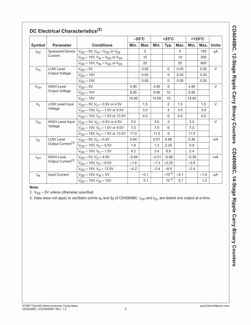
AC Electrical Characteristics(5)
CD4060BC TA = 25°C, CL = 50pF, RL = 200k, tr = tf = 20 ns, unless otherwise noted.
Note:5. AC Parameters are guaranteed by DC correlated testing.
RC Oscillator Notes:
Symbol Parameter Conditions Min. Typ. Max. Units
tPHL4, tPLH4 Propagation Delay Time to Q4 VDD = 5V 550 1300 ns
VDD = 10V 250 525
VDD = 15V 200 400
tPHL, tPLH Interstage Propagation Delay Time from Qn to Qn+1
VDD = 5V 150 330 ns
VDD = 10V 60 125
VDD = 15V 45 90
tTHL, tTLH Transition Time VDD = 5V 100 200 ns
VDD = 10V 50 100
VDD = 15V 40 80
tWL, tWH Minimum Clock Pulse Width VDD = 5V 170 500 ns
VDD = 10V 65 170
VDD = 15V 50 125
trCL, tfCL Maximum Clock Rise and Fall Time VDD = 5V No Limit ns
VDD = 10V No Limit
VDD = 15V No Limit
fCL Maximum Clock Frequency VDD = 5V 1 3 MHz
VDD = 10V 3 8
VDD = 15V 4 10
tPHL(R) Reset Propagation Delay VDD = 5V 200 450 ns
VDD = 10V 100 210
VDD = 15V 80 170
tWH(R) Minimum Reset Pulse Width VDD = 5V 200 450 ns
VDD = 10V 100 210
VDD = 15V 80 170
CIN Average Input Capacitance Any Input 5 7.5 pF
CPD Power Dissipation Capacitance 50 pF
1. R2 = 2 R1 to 10 R1
2. RC Oscillator applications are not recommended at supply voltages below 7.0V for R1 < 50kΩ
3. f ≈ 1
at VCC = 10V2.2 R1 CX

CD
4040BC
, 12-Stag
e Rip
ple C
arry Bin
ary Co
un
ters CD
4060BC
, 14-Stag
e Rip
ple C
arry Bin
ary Co
un
ters
©1987 Fairchild Semiconductor Corporation www.fairchildsemi.comCD4040BC, DCD4060BC Rev. 1.5 8
Physical Dimensions Dimensions are in millimeters unless otherwise noted.
Figure 1. 16-Lead Small Outline Integrated Circuit (SOIC), JEDEC MS-012, 0.150" NarrowPackage Number M16A

CD
4040BC
, 12-Stag
e Rip
ple C
arry Bin
ary Co
un
ters CD
4060BC
, 14-Stag
e Rip
ple C
arry Bin
ary Co
un
ters
©1987 Fairchild Semiconductor Corporation www.fairchildsemi.comCD4040BC, DCD4060BC Rev. 1.5 9
Physical Dimensions (Continued)Dimensions are in inches (millimeters) unless otherwise noted.
Figure 2. 16-Lead Plastic Dual-In-Line Package (PDIP), JEDEC MS-001, 0.300" WidePackage Number N16E

CD
4040BC
, 12-Stag
e Rip
ple C
arry Bin
ary Co
un
ters CD
4060BC
, 14-Stag
e Rip
ple C
arry Bin
ary Co
un
ters
©1987 Fairchild Semiconductor Corporation www.fairchildsemi.comCD4040BC, DCD4060BC Rev. 1.5 10
Rev. I28
TRADEMARKSThe following are registered and unregistered trademarks and service marks Fairchild Semiconductor owns or is authorized to use andis not intended to be an exhaustive list of all such trademarks
DISCLAIMERFAIRCHILD SEMICONDUCTOR RESERVES THE RIGHT TO MAKE CHANGES WITHOUT FURTHER NOTICE TO ANY PRODUCTSHEREIN TO IMPROVE RELIABILITY, FUNCTION, OR DESIGN. FAIRCHILD DOES NOT ASSUME ANY LIABILITY ARISING OUT OFTHE APPLICATION OR USE OF ANY PRODUCT OR CIRCUIT DESCRIBED HEREIN; NEITHER DOES IT CONVEY ANY LICENSEUNDER ITS PATENT RIGHTS, NOR THE RIGHTS OF OTHERS. THESE SPECIFICATIONS DO NOT EXPAND THE TERMS OFFAIRCHILD’S WORLDWIDE TERMS AND CONDITIONS, SPECIFICALLY THE WARRANTY THEREIN, WHICH COVERS THESEPRODUCTS.
LIFE SUPPORT POLICYFAIRCHILD’S PRODUCTS ARE NOT AUTHORIZED FOR USE AS CRITICAL COMPONENTS IN LIFE SUPPORT DEVICES ORSYSTEMS WITHOUT THE EXPRESS WRITTEN APPROVAL OF FAIRCHILD SEMICONDUCTOR CORPORATION.
As used herein:
1. Life support devices or systems are devices or systemswhich, (a) are intended for surgical implant into the body, or(b) support or sustain life, and (c) whose failure to performwhen properly used in accordance with instructions for useprovided in the labeling, can be reasonably expected to resultin significant injury to the user.
2. A critical component is any component of a life supportdevice or system whose failure to perform can be reasonablyexpected to cause the failure of the life support device orsystem, or to affect its safety or effectiveness.
PRODUCT STATUS DEFINITIONSDefinition of Terms
ACEx®
Build it Now™CorePLUS™CROSSVOLT™CTL™Current Transfer Logic™EcoSPARK®
FACT Quiet Series™FACT®
FAST®
FastvCore™FPS™FRFET®
Global Power ResourceSM
Green FPS™
Green FPS™ e-Series™GTO™i-Lo™IntelliMAX™ISOPLANAR™MegaBuck™MICROCOUPLER™MicroPak™Motion-SPM™OPTOLOGIC®
OPTOPLANAR®
PDP-SPM™Power220®
Power247®
POWEREDGE®
Power-SPM™PowerTrench®
Programmable Active Droop™QFET®
QS™QT Optoelectronics™Quiet Series™RapidConfigure™SMART START™SPM®
STEALTH™SuperFET™SuperSOT™-3SuperSOT™-6SuperSOT™-8
SyncFET™The Power Franchise®
™
TinyBoost™TinyBuck™TinyLogic®
TINYOPTO™TinyPower™TinyPWM™TinyWire™µSerDes™UHC®
UniFET™VCX™
Datasheet Identification Product Status Definition
Advance Information Formative or In Design This datasheet contains the design specifications for product development.Specifications may change in any manner without notice.
Preliminary First ProductionThis datasheet contains preliminary data; supplementary data will bepublished at a later date. Fairchild Semiconductor reserves the right to makechanges at any time without notice to improve design.
No Identification Needed Full Production This datasheet contains final specifications. Fairchild Semiconductor reservesthe right to make changes at any time without notice to improve design.
Obsolete Not In ProductionThis datasheet contains specifications on a product that has beendiscontinued by Fairchild semiconductor. The datasheet is printed forreference information only.