
A NON-INVERTING BUCK-BOOST CONVERTER WITH AN ...
14
FACTA UNIVERSITATIS Series: Electronics and Energetics Vol. 30, N o 1, March 2017, pp. 67 - 80 DOI: 10.2298/FUEE1701067L A NON-INVERTING BUCK-BOOST CONVERTER WITH AN ADAPTIVE DUAL CURRENT MODE CONTROL Srđan Lale 1 , Milomir Šoja 1 , Slobodan Lubura 1 , Dragan D. Mančić 2 , Milan Đ. Radmanović 2 1 University of East Sarajevo, Faculty of Electrical Engineering, East Sarajevo, Bosnia and Herzegovina 2 University of Niš, Faculty of Electronic Engineering, Niš, Serbia Abstract. This paper presents an implementation of adaptive dual current mode control (ADCMC) on non-inverting buck-boost converter. A verification of the converter operation with the proposed ADCMC has been performed in steady state and during the disturbances in the input voltage and the load resistance. The given simulation and experimental results confirm the effectiveness of the proposed control method. Key words: adaptive dual current mode control, non-inverting buck-boost converter, operating modes, transient response 1. INTRODUCTION A non-inverting buck-boost power electronics converter is one of the most versatile non-isolated converter topologies. It has become increasingly popular in many applications, including: electric vehicles [1], DC microgrids [2], battery-powered portable electronic devices (e.g. cellular phones and laptops) [3], [4], power factor correction (PFC) circuits [5], photovoltaic systems [6], etc. The non-inverting buck-boost converter provides the output voltage that is either lower or higher than the input voltage. This property is significant in so- called dynamic voltage scaling (DVS)-based power-efficient supplies, which provide adjustable voltage levels, according to the instantaneous operating conditions [7]. One of the most important features of this converter type is bidirectional operation, which is especially useful in applications such as DC microgrids and electric vehicles. The conventional two-switch topology of the non-inverting buck-boost converter is shown in Fig. 1 (a), being a result of a cascaded combination of a buck converter followed by a boost converter. It contains two power switches T 1 and T 2 . If a bidirectional operation of the non- inverting buck-boost converter is required, a four-switch topology from Fig. 1 (b) must be used, Received January 25, 2016; received in revised form April 10, 2016 Corresponding author: Srđan Lale University of East Sarajevo, Faculty of Electrical Engineering, Vuka Karadžića 30, 71126 Lukavica, East Sarajevo Bosnia and Herzegovina (E-mail: [email protected])
-
Upload
khangminh22 -
Category
Documents
-
view
0 -
download
0
Transcript of A NON-INVERTING BUCK-BOOST CONVERTER WITH AN ...
FACTA UNIVERSITATIS
Series: Electronics and Energetics Vol. 30, No 1, March 2017, pp. 67 - 80
DOI: 10.2298/FUEE1701067L
A NON-INVERTING BUCK-BOOST CONVERTER
WITH AN ADAPTIVE DUAL CURRENT MODE CONTROL
Srđan Lale1, Milomir Šoja
1, Slobodan Lubura
1,
Dragan D. Mančić2, Milan Đ. Radmanović
2
1University of East Sarajevo, Faculty of Electrical Engineering, East Sarajevo,
Bosnia and Herzegovina 2University of Niš, Faculty of Electronic Engineering, Niš, Serbia
Abstract. This paper presents an implementation of adaptive dual current mode control
(ADCMC) on non-inverting buck-boost converter. A verification of the converter operation
with the proposed ADCMC has been performed in steady state and during the disturbances
in the input voltage and the load resistance. The given simulation and experimental
results confirm the effectiveness of the proposed control method.
Key words: adaptive dual current mode control, non-inverting buck-boost converter,
operating modes, transient response
1. INTRODUCTION
A non-inverting buck-boost power electronics converter is one of the most versatile
non-isolated converter topologies. It has become increasingly popular in many applications,
including: electric vehicles [1], DC microgrids [2], battery-powered portable electronic
devices (e.g. cellular phones and laptops) [3], [4], power factor correction (PFC) circuits [5],
photovoltaic systems [6], etc. The non-inverting buck-boost converter provides the output
voltage that is either lower or higher than the input voltage. This property is significant in so-
called dynamic voltage scaling (DVS)-based power-efficient supplies, which provide adjustable
voltage levels, according to the instantaneous operating conditions [7]. One of the most
important features of this converter type is bidirectional operation, which is especially useful in
applications such as DC microgrids and electric vehicles.
The conventional two-switch topology of the non-inverting buck-boost converter is shown
in Fig. 1 (a), being a result of a cascaded combination of a buck converter followed by a boost
converter. It contains two power switches T1 and T2. If a bidirectional operation of the non-
inverting buck-boost converter is required, a four-switch topology from Fig. 1 (b) must be used,
Received January 25, 2016; received in revised form April 10, 2016
Corresponding author: Srđan Lale
University of East Sarajevo, Faculty of Electrical Engineering, Vuka Karadžića 30, 71126 Lukavica, East Sarajevo
Bosnia and Herzegovina
(E-mail: [email protected])

68 S. LALE, M. ŠOJA, S. LUBURA, D. D. MANĈIĆ, M. Đ. RADMANOVIĆ
where the diodes D1 and D2 from Fig. 1 (a) are replaced with additional power switches T3
and T4.
Fig. 1 A 2-switch (a) and 4-switch (b) topology of the non-inverting buck-boost converter
Depending on the ratio between the input voltage vg and the output voltage vo, the
non-inverting buck-boost converter can operate in buck mode (vo<vg) or boost mode
(vo>vg). As it is discussed in [8], these operating modes can be achieved in different ways.
A conventional way is to control simultaneously the switches T1 and T2 with the same gate
signal. Although this switching scheme is simple, it provides low converter efficiency. In
order to increase the efficiency, the operating modes are split: converter operates either as
buck converter (only switch T1 is controlled, while T2 is always turned off) when vo<vg or
boost converter (only switch T2 is controlled, while T1 is always turned on) when vo>vg.
However, the control of the switches is more complicated in this case, because it is
necessary to provide mode detection and smooth and stable transition between the modes.
Different control methods can be applied to the non-inverting buck-boost converter,
depending on the application. This paper is focused on using only current mode control
(CMC). In most cases, for example in [2], [3], [5], [9], regardless of the applied CMC
method, it is suggested that the non-inverting buck-boost converter operates either as
buck or boost converter, as described above. In [5], a non-inverting buck-boost converter
as a part of PFC rectifier works in both modes during fundamental period. After detection
of each operating mode, the built-in control logic decides to work as conventional peak
CMC (PCMC) or valley CMC (VCMC). Therefore, the control shifts between PCMC
(boost mode with duty cycle below 0.5) and VCMC (buck mode with duty cycle above
0.5) when the input rectified voltage crosses the output DC voltage, without need for
slope compensation. In [9] a synchronous buck-boost LED driver controller is presented,
which uses more complex control as a combination of PCMC and VCMC with slope
compensation.
However, as it is stated in [2], an implementation of conventional CMC methods to
this converter, such as PCMC and VCMC, is not a simple task, because they require
information about converter operating modes. An average CMC (ACMC) can be applied
to the non-inverting buck-boost converter, without determination of operating modes [2].
By using a dual-carrier modulator described in [2], it is possible to achieve a smooth
transition between the buck and the boost mode and to precisely control the inductor
current throughout the entire operating range. There are other ACMC approaches, for
example in [3], which unlike the above mentioned ACMC [2] has a mode selector circuit,
which determines the operating mode during a switching cycle.
Due to the inherent ability of natural transition between PCMC and VCMC and vice
versa, a dual current mode control (DCMC) proposed in [10] could be suitable for
implementation on the non-inverting buck-boost converter, with simultaneously controlled

A Non-inverting Buck-Boost Converter with an Adaptive Dual Current Mode Control 69
switches T1 and T2. The converter will operate in buck mode with PCMC (duty cycle below
0.5) and in boost mode with VCMC (duty cycle above 0.5). In this way, there is no need
for detection of operating modes. Also, the converter is stable for the entire range of duty
cycle from 0 to 1, that is, the subharmonic oscillations do not exist. On the other hand, all
excellent features of PCMC and VCMC are preserved, such as fixed switching frequency, good
dynamics and what is very important - simplicity.
A modified version of DCMC, named adaptive dual current mode control (ADCMC),
is proposed in [11] and elaborated in detail in [12], which improves some features of
DCMC, while the basic operating principles remain the same. In [12], only simulation
results are given for the non-inverting buck-boost converter. In this paper, besides some
simulation results, the experimental verification of ADCMC of this converter is presented.
The paper is organized in the following way. The basic operating principles of ADCMC, on
the example of the non-inverting buck-boost converter, are described in Section 2. The
simulation and experimental results are presented in Section 3. Section 4 gives the concluding
remarks.
2. OPERATING PRINCIPLES OF ADCMC OF NON-INVERTING BUCK-BOOST CONVERTER
The basic scheme of ADCMC of the conventional non-inverting buck-boost converter is
presented in Fig. 2 (a). The switches T1 and T2 are controlled simultaneously with the same
gate signal. In order to increase the converter efficiency, there is a possibility of synchronous
version of this converter, where the diodes D1 and D2 are replaced with power switches, as it
is shown in Fig. 1 (b). In this paper, a synchronous version is not used. However, as it is stated
in the Introduction, if bidirectional operation of the non-inverting buck-boost converter is
required, these additional two switches are necessary.
A quiescent value of the output voltage Vo of the non-inverting buck-boost converter
from Fig. 2 (a) is equal to:
,1
g
o
DVV
D
(1)
where D and Vg are the quiescent values of the duty cycle and the input voltage,
respectively. According to (1), when 0<D<0.5, the output voltage is lower than the input
voltage and the converter works in buck mode. When 0.5<D<1, the output voltage is
higher than the input voltage and the converter works in boost mode. If D=0.5, the input
and output voltages are equal.
By choosing PCMC for D<0.5 (buck mode) and VCMC for D>0.5 (boost mode), a stable
operation of the non-inverting buck-boost converter is guaranteed for the entire range of D
without slope compensation. Instead of mode detection and artificial shifting between
PCMC and VCMC, DCMC proposed in [10] is suitable for this application, because it
has a natural ability of shifting between PCMC, when D<0.5, and VCMC, when D>0.5,
without any mode selector circuits.
Similarly as PCMC and VCMC, DCMC has a drawback in existence of a peak-to-
average current error (a difference between the reference current iref and the average value
of the inductor current ( )s
L Ti t over switching period Ts). In ideal case of CMC, the aim is
70 S. LALE, M. ŠOJA, S. LUBURA, D. D. MANĈIĆ, M. Đ. RADMANOVIĆ
to control precisely the average value of the inductor current over each switching period, that is,
to make this error equal to zero. In order to eliminate peak-to-average current error, an
enhanced version of DCMC is proposed in [11], named ADCMC.
Fig. 2 a) ADCMC of the non-inverting buck-boost converter, b) Operating modes
A Non-inverting Buck-Boost Converter with an Adaptive Dual Current Mode Control 71
The operating modes of ADCMC applied to the non-inverting buck-boost converter
are shown in Fig. 2 (b). The main difference between ADCMC and DCMC is in the fact
that the width between peak iref+ib and valley iref-ib current boundaries (the current bandwidth
2ib), is not constant and predefined for ADCMC, unlike DCMC, but it is adaptive and online
calculated by using the instantaneous peak-to-peak ripple of the inductor current ΔiLpp on
each switching period Ts. The adaptive current bandwidth 2ib for the non-inverting buck-
boost converter is calculated as (Fig. 2 (a)):
2 ,( )
g o
b ib Lpp ib
s g o
v vi K i K
Lf v v
(2)
where Kib is the scaling gain (Kib≥1), fs=1/Ts is the switching frequency, and L is the
inductance value. The gain Kib determines whether 2ib≥ΔiLpp. When Kib=1, the adaptive
current bandwidth 2ib becomes equal to the measured instantaneous peak-to-peak current
ripple ΔiLpp, giving zero peak-to-average current error.
It is evident from (2) that the calculation of adaptive current bandwidth 2ib depends on
the inductance value L, which can be inconvenient if the L parameter is wrong or variable
in different operating conditions. The wrong L parameter will lead to inaccurate current
bandwidth 2ib and the appearance of the peak-to-average current error. A possible
solution for this issue is to directly measure the instantaneous peak-to-peak ripple from
the measured inductor current. This solution will be considered in the future work.
A detailed analysis of ADCMC, including small-signal models and design of the
output voltage compensator Gc(s) are presented in [12] for three types of DC–DC power
electronics converters: buck, boost, and non-inverting buck–boost converter. This paper is
focused on experimental verification of ADCMC of non-inverting buck-boost converter.
3. SIMULATION AND EXPERIMENTAL RESULTS
The operation of the non-inverting buck-boost converter under ADCMC, with the topology
from Fig. 2 (a), was verified with simulations in Matlab/Simulink and experimentally. The
parameters of the non-inverting buck-boost converter working in the continuous conduction
mode (CCM), which are the same for both simulations and experiments, are listed in Table 1.
The experimental setup is shown in Fig. 3. The developed setup can be used for testing
ADCMC on various types of converters, because the used prototype is made as a universal
four-quadrant (4Q) converter, with possibility of easy configuration to the desired topology,
such as buck, boost, non-inverting buck-boost, etc.
Table 1 Parameters of the non-inverting buck-boost converter
Vg [V] 12
L [µH] 220
C [µF] 1000
R [Ω] 20
fs [kHz] 23
72 S. LALE, M. ŠOJA, S. LUBURA, D. D. MANĈIĆ, M. Đ. RADMANOVIĆ
Fig. 3 Experimental setup: 1) The prototype of the non-inverting buck-boost converter; 2)
Electronic module for measurements and inner current loop; 3) PC with built-in
MF624 board; 4) Driver module; 5) Input voltage source of the converter;
6) Power supply units; 7) Tektronix MSO 2014 oscilloscope
A separate electronic module, which is connected to MF624 multifunctional data
acquisition input/output digital board [13], is used for implementation of the measurements
and inner current loop. The measurement of the inductor current, which is necessary for the
inner current loop, is performed with LEM current transducer HX 10-NP [14]. The converter
input and output voltage are measured with galvanic isolation via optocoupler IL300 [15] and
sampled by 14-bit A/D converter (conversion time about 2 µs) of the MF624 board. MF624
board is built into the computer and it provides a real time processing with Matlab/Simulink
environment. An implementation of the outer voltage loop and calculation of the adaptive
current bandwidth 2ib for ADCMC is performed in real time in Simulink, using Real Time
Windows Target (RTWT) environment. The reference current iref and current boundaries iref+ib
and iref-ib are obtained from 14-bit D/A converter of the MF624 board and fed into the inner
current loop. The fundamental sampling time for real time operation in Simulink was set to 25
μs, which is the minimum sampling time for this hardware.
Power MOSFETs IRF540N (100 V, 33 A) [16] are used as power switches T1 and T2.
A dual-channel galvanically isolated MOSFET driver module (turn on/off delay of 0.6 µs)
was developed for driving the power switches.
A Non-inverting Buck-Boost Converter with an Adaptive Dual Current Mode Control 73
A primary objective of the performed simulations and experiments is to demonstrate
that the proposed ADCMC can be successfully applied to the non-inverting buck-boost
converter, ensuring a stable operation in all operating modes and good dynamical properties,
regardless of the application. Several cases of the converter operation were tested: in steady
state for buck and boost operating modes, during the step changes in the input voltage and the
load resistance and during the gradual change of the input voltage.
3.1. Operation of the non-inverting buck-boost converter in steady state
The output compensator, as a key part of the outer voltage loop, produces the reference
current iref for the inner current loop (Fig. 2 (a)). In steady state, the reference current practically
has a constant value. Therefore, in order to test the behavior of the inner current loop in steady
state, the outer voltage loop can be disabled and the reference current should be set manually
as a constant signal.
A testing the operation of the non-inverting buck-boost converter with ADCMC in
steady state was performed for both cases: with and without the outer voltage loop. When
the voltage loop is disabled, two values of the reference current were used to provide buck and
boost operating mode. The simulation waveforms of the inductor current in steady state are
shown for ire f = 0.5 A (buck mode) in Fig. 4 (a) and iref = 5 A (boost mode) in Fig. 4 (b). The
corresponding experimental waveforms are given in Fig. 5 (a), (b).
In the second case, a simple proportional-integral (PI) compensator for the regulation
of the output voltage was employed. A design procedure for the output voltage compensator is
derived in detail in [12]. As in the first case, the both operating modes were considered. The
simulation waveforms of the inductor current in steady state are shown for two values of the
output voltage: vo = 7 V (buck mode) and vo = 30 V (boost mode), in Fig. 4 (c) and Fig. 4 (d),
respectively. The corresponding experimental results are presented in Fig. 5 (c), (d).
It is evident from Fig. 4 that there is an excellent matching between the reference
current and the average value of the inductor current. A very small peak-to-average current
error still exists, which can be attributed to the delays in numerical calculation of the simulation.
The experimental results from Fig. 5 are similar to the simulation results from Fig. 4.
A small peak-to-average current error appears as a consequence of imperfections of the
components used for realization of ADCMC.
On the basis of the given results from Fig. 4 and Fig. 5 it can be concluded that ADCMC
provide a stable operation of the non-inverting buck-boost converter for both values of the duty
cycle: D < 0.5 and D > 0.5.
3.2. Robustness to the disturbances in the input voltage and load
It is very important to evaluate how the converter with certain control is sensitive to
the various disturbances which can occur during operation. In this paper, the disturbances
such as the step and gradual changes of the input voltage and the step changes in the load
resistance were considered.
A line regulation, which is defined as converter ability to maintain the specified output
voltage despite changes in the input voltage, was tested for ADCMC of the non-inverting buck-
boost converter.

74 S. LALE, M. ŠOJA, S. LUBURA, D. D. MANĈIĆ, M. Đ. RADMANOVIĆ
Fig. 4 The simulation waveforms of the inductor current, reference current
and current boundaries in steady state, when the outer voltage loop is:
a), b) disabled; c), d) enabled
Fig. 5 The experimental waveforms of the inductor current, reference current
and current boundaries in steady state, when the outer voltage loop is:
a), b) disabled; c), d) enabled
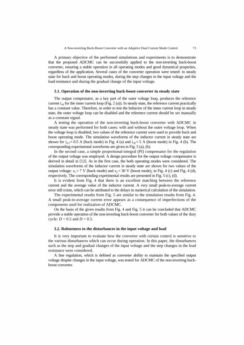
First, the step changes from 12 V to 6 V and vice versa, were introduced in the input
voltage. The output voltage was regulated to 9 V. The load resistance was set to R=10 Ω. These
step changes were performed in order to make a transition from buck to boost mode and vice
versa, and to examine the dynamical behavior of ADCMC. The waveforms of the output
voltage and the inductor current are shown in Fig. 6 (a), (b) (simulation) and Fig. 7
(experiment). The same parameters of the output voltage compensator were used in both
simulations and experiments.

A Non-inverting Buck-Boost Converter with an Adaptive Dual Current Mode Control 75
As it is shown from simulation and experimental results, the converter naturally crosses
from buck to boost mode and vice versa. Due to adaptation of the current bandwidth 2ib, the
transition of the inductor current from one mode to another is smooth, which gives satisfactory
line regulation.
Fig. 6 The simulation waveforms of the output voltage and the inductor current,
for the step changes in the input voltage (a), (b) and the load resistance (c), (d)
76 S. LALE, M. ŠOJA, S. LUBURA, D. D. MANĈIĆ, M. Đ. RADMANOVIĆ
Fig. 7 The experimental waveforms of the output voltage (up) and the inductor current
(bottom), when the input voltage changes from 12 V to 6 V (left) and vice versa (right)
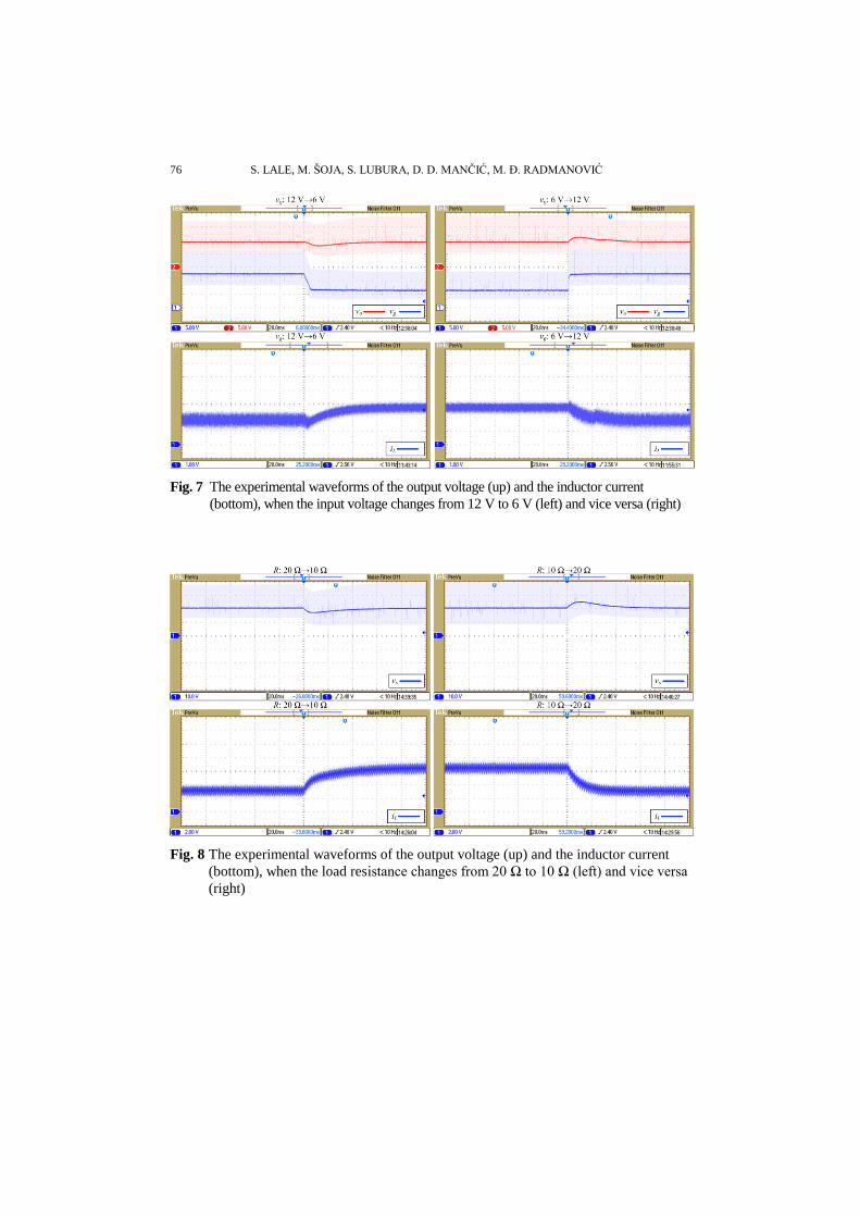
Fig. 8 The experimental waveforms of the output voltage (up) and the inductor current
(bottom), when the load resistance changes from 20 Ω to 10 Ω (left) and vice versa
(right)

A Non-inverting Buck-Boost Converter with an Adaptive Dual Current Mode Control 77
Fig. 9 The experimental waveforms of the output voltage, when the input voltage
changes from 6 V to 12 V (up) and vice versa (bottom), for σ=100, 150, 200 and 500
Fig. 10 The experimental waveforms of the output voltage, when the load resistance changes
from 10 Ω to 20 Ω (up) and vice versa (bottom), for σ=100, 150, 200 and 500

78 S. LALE, M. ŠOJA, S. LUBURA, D. D. MANĈIĆ, M. Đ. RADMANOVIĆ
In order to test a step load response, step changes in the load resistance from R=20 Ω to
R=10 Ω and vice versa were performed. The output voltage was regulated to 20 V. The
simulation and experimental waveforms of the output voltage and the inductor current are
shown in Fig. 6 (c), (d) and Fig. 8, respectively. It is evident that ADCMC successfully reject
the introduced load disturbances.
The transient response in the output voltage for the considered step disturbances depends
also on the designed output voltage compensator, as it is shown in Fig. 9 and Fig. 10. Several
values of parameter σ, which determines the transient response time (about 5/σ) and the gains of
the PI compensator [12], are considered.
It is evident from the given experimental results from Fig. 9 and Fig. 10 that better
responses regarding the transient response time and over/undershoot are obtained for higher
values of the adjustable parameter σ.
The optimization of the output voltage compensator is not subject in this paper. The aim
was to obtain satisfactory results in accordance with the design procedure from [12] (the
chosen settling time is about 10-50 ms). Also, the output voltage loop is designed to be
slow in order to emphasize the behavior of the inner current loop.
Fig. 11 The experimental waveforms of the output voltage (up) and the inductor current
(bottom), for the gradual change of the input voltage from 15 V to 5 V (left) and
vice versa (right)
Besides the step changes, a gradual linear change in the input voltage was also introduced in
the experiments. The input voltage was gradually changed from 15 V to 5 V and vice versa,
while the output voltage was regulated to 10 V, in order to make a gradual transition from buck
to boost mode and vice versa. The experimental results are shown in Fig. 11. It is obvious
that ADCMC is robust against these changes. The output voltage is successfully regulated,
without any disruptions between two operating modes.
A Non-inverting Buck-Boost Converter with an Adaptive Dual Current Mode Control 79
4. CONCLUSION
In this paper, an implementation of a novel ADCMC method on the non-inverting
buck-boost converter has been presented. The given simulation and experimental results
confirm that there is no need for the detection of converter operating modes, because this
method ensures a natural and stable transition between the buck and the boost mode, and
vice versa. The given results show that ADCMC provides a stable operation of the non-
inverting buck-boost converter for the entire range of duty cycle from 0 to 1. Also, it is
robust against the disturbances, such as the step and gradual changes in the input voltage
and the step changes in the load resistance, with good dynamical performances.
The following task will be the using of the proposed ADCMC of the non-inverting buck-
boost converter in various popular applications, such as battery chargers/dischargers, LED
drivers, etc., and to compare it with other relevant methods in the same applications.
REFERENCES
[1] M. A. Khan, A. Ahmed, I. Husain, Y. Sozer and M. Badawy, "Performance Analysis of Bidirectional
DC–DC Converters for Electric Vehicles", IEEE Trans. Ind. Appl., vol. 51, no. 4, pp. 3442-3452,
July/Aug. 2015.
[2] I. Aharon, A. Kuperman and D. Shmilovitz, "Analysis of Dual-Carrier Modulator for Bidirectional
Noninverting Buck–Boost Converter", IEEE Trans. Power Electron., vol. 30, no. 2, pp. 840-848, Feb.
2015.
[3] Wei Chia-Ling, Chen Chin-Hong, Wu Kuo-Chun and Ko I-Ting, "Design of an Average-Current-Mode
Noninverting Buck–Boost DC–DC Converter With Reduced Switching and Conduction Losses", IEEE
Trans. Power Electron., vol. 27, no. 12, pp. 4934-4943.
[4] C.-H. Tsai, Y.-S. Tsai and H.-C. Liu, "A Stable Mode-Transition Technique for a Digitally Controlled
Non-Inverting Buck–Boost DC–DC Converter", IEEE Trans. Ind. Electron., vol. 62, no. 1, pp. 475-483,
Jan. 2015.
[5] G. K. Andersen and F. Blaabjerg, "Current programmed control of a single-phase two-switch buck-boost
power factor correction circuit", IEEE Trans. Ind. Electron., vol. 53, no. 1, pp. 263-271, Feb. 2006.
[6] T.-F. Wu, C.-L. Kuo, K.-H. Sun, Y.-K. Chen, Y.-R. Chang and Y.-D. Lee, "Integration and Operation of
a Single-Phase Bidirectional Inverter With Two Buck/Boost MPPTs for DC-Distribution Applications",
IEEE Trans. Power Electron., vol. 28, no. 11, pp. 5098-5106, Nov. 2013.
[7] L. Feng and M. Dongsheng, "Design of Digital Tri-mode Adaptive-Output Buck–Boost Power Converter
for Power-Efficient Integrated Systems", IEEE Trans. Ind. Electron., vol. 57, no. 6, pp. 2151-2160, June
2010.
[8] Haifeng Fan, "Design tips for an efficient non-inverting buck-boost converter", Analog Applications
Journal, Texas Instruments, pp. 20-25, 2014.
[9] Linear Technology, "60V 4-Switch Synchronous Buck-Boost LED Driver Controller", LT3791
datasheet, Rev. B, 2012. Available: http://cds.linear.com/docs/en/datasheet/3791fb.pdf.
[10] A. V. Anunciada and M. M. Silva, "A new current mode control process and applications", IEEE Trans.
Power Electron., vol. 6, no. 4, pp. 601–610, Oct. 1991.
[11] S. Lale, M. Šoja, S. Lubura and M. Radmanović, "Modeling and analysis of new adaptive dual current
mode control", In Proceedings of the 10th International Symposium on Industrial Electronics INDEL
2014, vol. 10, no. T-02, pp. 73–76.
[12] Available: http://www.indel.etfbl.net/resources/Proceedings_2014/INDEL_2014_Paper_11.pdf.
[13] S. Lale, M. Šoja and S. Lubura, "A modified dual current mode control method with an adaptive current
bandwidth", Int. J. Circ. Theor. Appl., 2015.
[14] HUMUSOFT, "MF624 Multifunction I/O Card", MF624 user’s manual, 2014. Available:
http://www2.humusoft.cz/www/datacq/manuals/mf624um.pdf.
[15] LEM, "Current Transducer HX 05..15-NP", HX 10-NP datasheet. Available: http://www.lem.com/docs/
products/hx%205_15-np_e%20v10.pdf.

80 S. LALE, M. ŠOJA, S. LUBURA, D. D. MANĈIĆ, M. Đ. RADMANOVIĆ
[16] Vishay Semiconductors, "Linear Optocoupler, High Gain Stability, Wide Bandwidth", IL300 datasheet.
Available: http://www.vishay.com/docs/83622/il300.pdf.
[17] International Rectifier, "HEXFET® Power MOSFET", IRF540N datasheet. Available: http://www.irf.com/
product-info/datasheets/data/irf540n.pdf.