LP873220-Q1 Dual High-Current Buck Converter and Dual ...
78
LP873220-Q1 Dual High-Current Buck Converter and Dual Linear Regulator 1 Features • AEC-Q100 qualified with the following results: – Device temperature grade 1: –40°C to +125°C ambient operating temperature • Input voltage: 2.8 V to 5.5 V • Two high-efficiency step-down DC/DC converters: – Output voltage: 0.7 V to 3.36 V – Maximum output current 2 A – Programmable output-voltage slew rate from 0.5 mV/µs to 10 mV/µs – 2-MHz switching frequency – Spread-spectrum mode and phase interleaving for EMI reduction • Two linear regulators: – Input voltage: 2.5 V to 5.5 V – Output voltage: 0.8 V to 3.3 V – Maximum output current 300 mA • Configurable general-purpose output signals (GPO, GPO2) • Interrupt function with programmable masking • Programmable power-good signal (PGOOD) • Output short-circuit and overload protection • Overtemperature warning and protection • Overvoltage protection (OVP) and undervoltage lockout (UVLO) • 28-pin, 5-mm × 5-mm VQFN package with wettable flanks SW_B0 VIN_B0 VIN_B1 VANA VIN FB_B0 VOUT_B0 LOAD SDA SCL nINT CLKIN (GPO2) GNDs EN GPO SW_B1 FB_B1 VOUT_B1 LOAD PGOOD VOUT_LDO1 VOUT_LDO0 VIN_LDO0 VIN_LDO1 VOUT_LDO0 VOUT_LDO1 Copyright © 2017, Texas Instruments Incorporated Simplified Schematic 2 Applications • Automotive head unit and cluster • Automotive camera module • Surround view system ECU • Radar system ECU • Automotive display 3 Description The LP873220-Q1 is designed to meet the power management requirements of the latest processors and platforms in automotive camera and radar applications. The device has two step-down DC/DC converters, two linear regulators, and two general-purpose digital-output signals. The device is controlled by an I 2 C-compatible serial interface and by an enable signal. The automatic PWM/PFM (AUTO mode) operation gives high efficiency over a wide output-current range. The LP873220-Q1 supports remote voltage sensing to compensate IR drop between the regulator output and the point-of-load (POL), thus improving the accuracy of the output voltage. In addition, the switching clock can be forced to PWM mode and also synchronized to an external clock to minimize the disturbances. The LP873220-Q1 device also supports programmable start-up and shutdown delays and sequences including GPO signals synchronized to the enable signal. During start-up and voltage change, the device controls the output slew rate to minimize output voltage overshoot and the in-rush current. Device Information (1) PART NUMBER PACKAGE BODY SIZE (NOM) LP873220-Q1 VQFN (28) 5.00 mm × 5.00 mm (1) For all available packages, see the orderable addendum at the end of the data sheet. Output Current (A) Efficiency (%) 0.001 0.01 0.1 1 2 50 60 70 80 90 100 D002 Vin=3.7V, Vout=1.0V Vin=3.7V, Vout=1.8V Vin=3.7V, Vout=2.5V DC/DC Efficiency vs Output Current LP873220-Q1 SNVSAT4A – SEPTEMBER 2017 – REVISED JUNE 2021 An IMPORTANT NOTICE at the end of this data sheet addresses availability, warranty, changes, use in safety-critical applications, intellectual property matters and other important disclaimers. PRODUCTION DATA.
-
Upload
khangminh22 -
Category
Documents
-
view
4 -
download
0
Transcript of LP873220-Q1 Dual High-Current Buck Converter and Dual ...

LP873220-Q1 Dual High-Current Buck Converter and Dual Linear Regulator
1 Features• AEC-Q100 qualified with the following results:
– Device temperature grade 1: –40°C to +125°C ambient operating temperature
• Input voltage: 2.8 V to 5.5 V• Two high-efficiency step-down DC/DC converters:
– Output voltage: 0.7 V to 3.36 V– Maximum output current 2 A– Programmable output-voltage slew rate from
0.5 mV/µs to 10 mV/µs– 2-MHz switching frequency– Spread-spectrum mode and phase interleaving
for EMI reduction• Two linear regulators:
– Input voltage: 2.5 V to 5.5 V– Output voltage: 0.8 V to 3.3 V– Maximum output current 300 mA
• Configurable general-purpose output signals (GPO, GPO2)
• Interrupt function with programmable masking• Programmable power-good signal (PGOOD)• Output short-circuit and overload protection• Overtemperature warning and protection• Overvoltage protection (OVP) and undervoltage
lockout (UVLO)• 28-pin, 5-mm × 5-mm VQFN package with
wettable flanks
SW_B0VIN_B0
VIN_B1
VANA
VIN
FB_B0
VOUT_B0LOAD
SDA
SCL
nINT
CLKIN (GPO2)
GNDs
EN
GPO
SW_B1
FB_B1
VOUT_B1LOAD
PGOOD
VOUT_LDO1
VOUT_LDO0
VIN_LDO0
VIN_LDO1
VOUT_LDO0
VOUT_LDO1
Copyright © 2017, Texas Instruments Incorporated
Simplified Schematic
2 Applications• Automotive head unit and cluster• Automotive camera module• Surround view system ECU• Radar system ECU• Automotive display
3 DescriptionThe LP873220-Q1 is designed to meet the power management requirements of the latest processors and platforms in automotive camera and radar applications. The device has two step-down DC/DC converters, two linear regulators, and two general-purpose digital-output signals. The device is controlled by an I2C-compatible serial interface and by an enable signal.
The automatic PWM/PFM (AUTO mode) operation gives high efficiency over a wide output-current range. The LP873220-Q1 supports remote voltage sensing to compensate IR drop between the regulator output and the point-of-load (POL), thus improving the accuracy of the output voltage. In addition, the switching clock can be forced to PWM mode and also synchronized to an external clock to minimize the disturbances.
The LP873220-Q1 device also supports programmable start-up and shutdown delays and sequences including GPO signals synchronized to the enable signal. During start-up and voltage change, the device controls the output slew rate to minimize output voltage overshoot and the in-rush current.
Device Information(1)
PART NUMBER PACKAGE BODY SIZE (NOM)LP873220-Q1 VQFN (28) 5.00 mm × 5.00 mm
(1) For all available packages, see the orderable addendum at the end of the data sheet.
Output Current (A)
Effic
iency (
%)
0.001 0.01 0.1 1 250
60
70
80
90
100
D002
Vin=3.7V, Vout=1.0VVin=3.7V, Vout=1.8VVin=3.7V, Vout=2.5V
DC/DC Efficiency vs Output Current
LP873220-Q1SNVSAT4A – SEPTEMBER 2017 – REVISED JUNE 2021
An IMPORTANT NOTICE at the end of this data sheet addresses availability, warranty, changes, use in safety-critical applications, intellectual property matters and other important disclaimers. PRODUCTION DATA.
Table of Contents1 Features............................................................................12 Applications..................................................................... 13 Description.......................................................................14 Revision History.............................................................. 25 Pin Configuration and Functions...................................36 Specifications.................................................................. 5
6.1 Absolute Maximum Ratings........................................ 56.2 ESD Ratings............................................................... 56.3 Recommended Operating Conditions.........................56.4 Thermal Information....................................................66.5 Electrical Characteristics.............................................66.6 I2C Serial Bus Timing Parameters............................ 116.7 Typical Characteristics.............................................. 14
7 Detailed Description......................................................157.1 Overview................................................................... 157.2 Functional Block Diagram......................................... 167.3 Feature Description...................................................167.4 Device Functional Modes..........................................34
7.5 Programming............................................................ 357.6 Register Maps...........................................................38
8 Application and Implementation.................................. 598.1 Application Information............................................. 598.2 Typical Application.................................................... 59
9 Power Supply Recommendations................................6610 Layout...........................................................................67
10.1 Layout Guidelines................................................... 6710.2 Layout Example...................................................... 68
11 Device and Documentation Support..........................6911.1 Device Support........................................................6911.2 Receiving Notification of Documentation Updates.. 6911.3 Support Resources................................................. 6911.4 Trademarks............................................................. 6911.5 Electrostatic Discharge Caution.............................. 6911.6 Glossary.................................................................. 69
12 Mechanical, Packaging, and Orderable Information.................................................................... 69
4 Revision HistoryNOTE: Page numbers for previous revisions may differ from page numbers in the current version.
Changes from Revision * (September 2017) to Revision A (June 2021) Page• Updated the numbering format for tables, figures, and cross-references throughout the document..................1• Updated the LDO Output Capacitor Selection section..................................................................................... 61
LP873220-Q1SNVSAT4A – SEPTEMBER 2017 – REVISED JUNE 2021 www.ti.com
2 Submit Document Feedback Copyright © 2021 Texas Instruments Incorporated
Product Folder Links: LP873220-Q1

5 Pin Configuration and Functions
8
9
10
11
12
13
14
2 3 4 5 61 7
20 19 18 17 1621 15
28
27
26
25
24
23
22
VIN_LDO1
nINT
CLKIN
VIN_B1
VIN_B1
SW_B1
SW_B1
PG
ND
_B
1
PG
ND
_B
1
SC
L
SD
A
SG
ND
PG
ND
_B
0
PG
ND
_B
0
VO
UT
_L
DO
1
EN
VA
NA
AG
ND
FB
_B
1
FB
_B
0
VO
UT
_L
DO
0
SW_B0
SW_B0
VIN_B0
VIN_B0
GPO
PGOOD
VIN_LDO0
THERMAL PAD
Figure 5-1. RHD Package 28-Pin VQFN With Thermal Pad Top View
Table 5-1. Pin FunctionsPIN
TYPE(1) DESCRIPTIONNUMBER NAME1 VOUT_LDO0 P/O LDO0 output. If the LDO0 is not used, leave the pin floating.
2 FB_B0 A Output voltage feedback (positive) for Buck 0.
3 FB_B1 A Output voltage feedback (positive) for Buck 1
4 AGND G Ground.
5 VANA P/I Supply voltage for analog and digital blocks. Must be connected to same node with VIN_Bx.
6 EN D/I Programmable enable signal for regulators and GPOs. If the pin is not used, leave the pin floating.
7 VOUT_LDO1 P/O LDO1 output. If LDO1 is not used, leave the pin floating.
8 VIN_LDO1 P/I Power input for LDO1. If LDO1 is not used, connect the pin to VANA.
9 nINT D/O Open-drain interrupt output. Active LOW. If the pin is not used, connect the pin to ground.
10 CLKIN D/I/O External clock input. Alternative function is general-purpose digital output (GPO2). If the pin is not used, leave the pin floating.
11, 12 VIN_B1 P/I Input for Buck 1. The separate power pins VIN_Bx are not connected together internally - VIN_Bx pins must be connected together in the application and be locally bypassed.
13, 14 SW_B1 P/O Buck 1 switch node. If the Buck 1 is not used, leave the pin floating.
15, 16 PGND_B1 P/G Power ground for Buck 1.
17 SCL D/I Serial interface clock input for I2C access. Connect a pullup resistor. If the I2C interface is not used, connect the pin to Ground.
18 SDA D/I/O Serial interface data input and output for I2C access. Connect a pullup resistor. If the I2C interface is not used, connect the pin to Ground.
19 SGND G Ground.
20, 21 PGND_B0 P/G Power ground for Buck 0.
22, 23 SW_B0 P/O Buck 0 switch node. If the Buck 0 is not used, leave the pin floating.
www.ti.comLP873220-Q1
SNVSAT4A – SEPTEMBER 2017 – REVISED JUNE 2021
Copyright © 2021 Texas Instruments Incorporated Submit Document Feedback 3
Product Folder Links: LP873220-Q1

Table 5-1. Pin Functions (continued)PIN
TYPE(1) DESCRIPTIONNUMBER NAME
24, 25 VIN_B0 P/I Input for Buck 0. The separate power pins VIN_Bx are not connected together internally - VIN_Bx pins must be connected together in the application and be locally bypassed.
26 GPO D/O General-purpose digital output. If the pin is not used, leave the pin floating.
27 PGOOD D/O Power-good indication signal. If the pin is not used, leave the pin floating.
28 VIN_LDO0 P/I Power input for LDO0. If the LDO0 is not used, connect the pin to VANA.
Thermal Pad — — Connect to PCB ground plane using multiple vias for good thermal performance.
(1) A: Analog Pin, D: Digital Pin, G: Ground Pin, P: Power Pin, I: Input Pin, and O: Output Pin.
LP873220-Q1SNVSAT4A – SEPTEMBER 2017 – REVISED JUNE 2021 www.ti.com
4 Submit Document Feedback Copyright © 2021 Texas Instruments Incorporated
Product Folder Links: LP873220-Q1
6 Specifications6.1 Absolute Maximum RatingsOver operating free-air temperature range (unless otherwise noted)(1) (2)
MIN MAX UNIT
VIN_Bx, VANA Voltage on power connections (must use the same input supply) –0.3 6 V
VIN_LDOx Voltage on power connections –0.3 6 V
SW_Bx Voltage on buck switch nodes –0.3 (VIN_Bx + 0.3 V) with 6-V maximum V
FB_Bx Voltage on buck voltage sense nodes –0.3 (VANA + 0.3 V) with 6-V maximum V
VOUT_LDOx Voltage on LDO output -0.3 (VIN_LDOx + 0.3 V) with 6-V maximum V
SDA, SCL, nINT, EN Voltage on logic pins (input or output pins) –0.3 6 V
PGOOD, GPO, CLKIN (GPO2) Voltage on logic pins (input or output pins) –0.3 (VANA + 0.3 V) with 6-V
maximum V
TJ-MAX Junction temperature −40 150
°CTstg Storage temperature –65 150
Maximum lead temperature (soldering, 10 seconds) 260
(1) Stresses beyond those listed under Absolute Maximum Ratings may cause permanent damage to the device. These are stress ratings only, which do not imply functional operation of the device at these or any other conditions beyond those indicated under Section 6.3. Exposure to absolute-maximum-rated conditions for extended periods may affect device reliability.
(2) All voltage values are with respect to network ground.
6.2 ESD RatingsVALUE UNIT
V(ESD) Electrostatic discharge
Human-body model (HBM), per AEC Q100-002(1) ±2000
VCharged-device model (CDM), per AEC Q100-011
All pins ±500
Corner pins (1, 7, 8, 14, 15, 21, 22, 28)
±750
(1) AEC Q100-002 indicates that HBM stressing shall be in accordance with the ANSI/ESDA/JEDEC JS-001 specification.
6.3 Recommended Operating ConditionsOver operating free-air temperature range (unless otherwise noted)
MIN MAX UNITINPUT VOLTAGE
VIN_Bx, VANA Voltage on power connections (must use the same input supply) 2.8 5.5 V
VIN_LDOx Voltage on LDO inputs 2.5 5.5 V
EN, nINT Voltage on logic pins (input or output pins) 0 5.5 V
CLKIN Voltage on logic pins (input pin) 0 VANA with 5.5-V maximum V
PGOOD, GPO, GPO2 Voltage on logic pins (output pins) 0 VANA V
SCL, SDA
Voltage on I2C interface, Standard (100 kHz), Fast (400 kHz), Fast+ (1 MHz), and High-Speed (3.4 MHz) Modes 0 1.95 V
Voltage on I2C interface, Standard (100 kHz), Fast (400 kHz), and Fast+ (1 MHz) Modes 0 VANA with 3.6-V
maximum V
TEMPERATURETJ Junction temperature −40 140 °C
TA Ambient temperature −40 125 °C
www.ti.comLP873220-Q1
SNVSAT4A – SEPTEMBER 2017 – REVISED JUNE 2021
Copyright © 2021 Texas Instruments Incorporated Submit Document Feedback 5
Product Folder Links: LP873220-Q1

6.4 Thermal Information
THERMAL METRIC(1)
LP873220-Q1UNITRHD (VQFN)
28 PINSRθJA Junction-to-ambient thermal resistance 36.7 °C/W
RθJCtop Junction-to-case (top) thermal resistance 26.6 °C/W
RθJB Junction-to-board thermal resistance 8.9 °C/W
ψJT Junction-to-top characterization parameter 0.4 °C/W
ψJB Junction-to-board characterization parameter 8.8 °C/W
RθJCbot Junction-to-case (bottom) thermal resistance 2.2 °C/W
(1) For more information about traditional and new thermal metrics, see the Semiconductor and IC Package Thermal Metrics application note.
6.5 Electrical CharacteristicsLimits apply over the junction temperature range –40°C ≤ TJ ≤ +140°C, specified VVANA, VVIN_Bx, VVIN_LDOx, VVOUT_Bx, VVOUT_LDOx and IOUT range, unless otherwise noted. Typical values are at TJ = 25°C, VVANA = VVIN_Bx = VVIN_LDOx = 3.7 V, and VOUT = 1 V, unless otherwise noted(1) (2).
PARAMETER TEST CONDITIONS MIN TYP MAX UNITEXTERNAL COMPONENTS
CIN_BUCK
Input filtering capacitance for buck regulators
Effective capacitance, connected from VIN_Bx to PGND_Bx 1.9 10 µF
COUT_BUCK
Output filtering capacitance for buck regulators
Effective capacitance 10 22 500 µF
CPOL_BUCK
Point-of-load (POL) capacitance for buck regulators
Optional POL capacitance 22 µF
COUT-TOTAL_BUCK
Buck output capacitance, total (local and POL) Total output capacitance 500 µF
CIN_LDO
Input filtering capacitance for LDO regulators
Effective capacitance, connected from VIN_LDOx to AGND. CIN_LDO must be at least two times larger than COUT_LDO
0.6 2.2 µF
COUT_LDO
Output filtering capacitance for LDO regulators
Effective capacitance 0.4 1 2.7 µF
ESRCInput and output capacitor ESR [1-10] MHz 2 10 mΩ
L Inductor Inductance of the inductor0.47
µH–30% 30%
DCRL Inductor DCR 25 mΩ
BUCK REGULATORSV(VIN_Bx), V(VANA)
Input voltage range VIN_Bx and VANA pins must be connected to the same supply line 2.8 3.7 5.5 V
VOUT_Bx Output voltage
Programmable voltage range 0.7 1 3.36 V
Step size, 0.7 V ≤ VOUT < 0.73 V 10
mVStep size, 0.73 V ≤ VOUT < 1.4 V 5
Step size, 1.4 V ≤ VOUT ≤ 3.36 V 20
IOUT_Bx Output current Output current 2(3) A
Input and Output voltage difference
Minimum voltage between V(VIN_Bx) and VOUT to fulfill the electrical characteristics 0.8 V
LP873220-Q1SNVSAT4A – SEPTEMBER 2017 – REVISED JUNE 2021 www.ti.com
6 Submit Document Feedback Copyright © 2021 Texas Instruments Incorporated
Product Folder Links: LP873220-Q1

6.5 Electrical Characteristics (continued)Limits apply over the junction temperature range –40°C ≤ TJ ≤ +140°C, specified VVANA, VVIN_Bx, VVIN_LDOx, VVOUT_Bx, VVOUT_LDOx and IOUT range, unless otherwise noted. Typical values are at TJ = 25°C, VVANA = VVIN_Bx = VVIN_LDOx = 3.7 V, and VOUT = 1 V, unless otherwise noted(1) (2).
PARAMETER TEST CONDITIONS MIN TYP MAX UNIT
VOUT_Bx_DC
DC output voltage accuracy, includes voltage reference, DC load and line regulations, process and temperature
Force PWM mode, VOUT < 1 V –20 20 mV
Force PWM mode, VOUT ≥ 1 V –2% 2%
PFM mode, VOUT < 1 V, the average output voltage level is increased by max. 20 mV –20 40 mV
PFM mode, VOUT ≥ 1 V, the average output voltage level is increased by max. 20 mV –2% 2% + 20
mV
Ripple voltagePWM mode 10
mVp-pPFM mode, IOUT = 10 mA 25
DCLNR DC line regulation IOUT = 1 A ±0.05 %/V
DCLDRDC load regulation in PWM mode VOUT_Bx = 1 V, IOUT from 0 to IOUT(max) 0.3%
TLDSRTransient load step response
IOUT = 0.1 A to 2 A, TR = TF = 400 ns, PWM mode
±55 mV
TLNSR Transient line response V(VIN_Bx) stepping 3 V ↔ 3.5 V, TR = TF = 10 µs, IOUT = IOUT(max)
±10 mV
ILIM FWD
Forward current limit per phase (peak for every switching cycle)
Programmable range 1.5 3A
Step size 0.5
Accuracy, V(VIN_Bx) ≥ 3 V, ILIM = 3 A –5% 7.5% 20%
Accuracy, 2.8 V ≤ V(VIN_Bx) < 3 V, ILIM = 3 A –20% 7.5% 20%
ILIM NEGNegative current limit per phase 1.6 2.0 3.0 A
RDS(ON) HS FETOn-resistance, high-side FET
Each phase, between VIN_Bx and SW_Bx pins (I = 1 A) 50 110 mΩ
RDS(ON) LS FETOn-resistance, low-side FET
Each phase, between SW_Bx and PGND_Bx pins (I = 1 A) 45 90 mΩ
ƒSW Switching frequency PWM mode 1.8 2 2.2 MHz
Start-up time (soft start) From ENx to VOUT_Bx = 0.35 V (slew-rate control begins) 120 µs
Output voltage slew-rate(4)
SLEW_RATEx[2:0] = 010, COUT-TOTAL_BUCK < 80 µF
–15%
10
15% mV/µs
SLEW_RATEx[2:0] = 011, COUT-TOTAL_BUCK < 130 µF 7.5
SLEW_RATEx[2:0] = 100, COUT-TOTAL_BUCK < 250 µF 3.8
SLEW_RATEx[2:0] = 101, COUT-TOTAL_BUCK < 500 µF 1.9
SLEW_RATEx[2:0] = 110, COUT-TOTAL_BUCK < 500 µF 0.94
SLEW_RATEx[2:0] = 111, COUT-TOTAL_BUCK < 500 µF 0.47
IPFM-PWMPFM-to-PWM - current threshold(5) 550 mA
IPWM-PFMPWM-to-PFM - current threshold(5) 290 mA
RDIS_BxOutput pulldown resistance Regulator disabled 150 250 350 Ω
www.ti.comLP873220-Q1
SNVSAT4A – SEPTEMBER 2017 – REVISED JUNE 2021
Copyright © 2021 Texas Instruments Incorporated Submit Document Feedback 7
Product Folder Links: LP873220-Q1

6.5 Electrical Characteristics (continued)Limits apply over the junction temperature range –40°C ≤ TJ ≤ +140°C, specified VVANA, VVIN_Bx, VVIN_LDOx, VVOUT_Bx, VVOUT_LDOx and IOUT range, unless otherwise noted. Typical values are at TJ = 25°C, VVANA = VVIN_Bx = VVIN_LDOx = 3.7 V, and VOUT = 1 V, unless otherwise noted(1) (2).
PARAMETER TEST CONDITIONS MIN TYP MAX UNIT
Output voltage monitoring for PGOOD pin and for power-good Interrupt
V(VIN_Bx) and V(VANA) fixed 3.7 V
Overvoltage threshold (compared to DC output voltage level, VVOUT_Bx_DC) 39 50 64
mVUndervoltage threshold (compared to DC output voltage level, VVOUT_Bx_DC) –53 –40 –29
Deglitch time during operation and after voltage change 4 15 µs
Gating time for PGOOD signal after regulator enable or voltage change
PGOOD_MODE = 0 800 µs
LDO REGULATORS
VIN_LDOxInput voltage range for LDO power inputs VIN_LDOx can be higher or lower than V(VANA) 2.5 3.7 5.5 V
VOUT_LDOx Output voltageProgrammable voltage range 0.8 3.3
VStep size 0.1
IOUT_LDOx Output current 300 mA
Dropout voltageV(VIN_LDOx) – V(VOUT_LDOx), IOUT = IOUT(max), Programmed output voltage is higher than V(VIN_LDOx)
200 mV
VOUT_LDO_DC
DC output voltage accuracy, includes voltage reference, DC load and line regulations, process, temperature
VOUT < 1 V –20 20 mV
VOUT ≥ 1 V –2% 2%
DCLNR DC line regulation IOUT = 1 mA 0.1 %/V
DCLDR DC load regulation IOUT = 1 mA to IOUT(max) 0.8%
TLDSRTransient load step response IOUT = 1 mA to 300 mA, TR = TF = 1 µs –50/+40 mV
TLNSR Transient line response V(VIN_LDOx) stepping 3 V ↔ 3.5 V, TR = TF = 10 µs, IOUT = IOUT(max)
±7 mV
PSRR Power supply ripple rejection ƒ = 10 kHz, IOUT = IOUT(max) 53 dB
Noise 10 Hz < F < 100 kHz, IOUT = IOUT(max) 82 µVrms
ISHORT(LDOx) LDO current limit VOUT = 0 V 400 500 600 mA
Start-up time From enable to valid output voltage 300 µs
Slew rate during start-up 15 mV/µs
RDIS_LDOxOutput pulldown resistance Regulator disabled 150 250 350 Ω
Output voltage monitoring for PGOOD pin and for power-good interrupt
Overvoltage monitoring, voltage rising (compared to DC output voltage level, VOUT_LDO_DC)
106% 108% 110%
Overvoltage monitoring, hysteresis 3% 3.5% 4%
Undervoltage monitoring, voltage falling (compared to DC output voltage level, VOUT_LDO_DC)
90% 92% 94%
Undervoltage monitoring, hysteresis 3% 3.5% 4%
Deglitch time during operation and after voltage change 4 15 µs
LP873220-Q1SNVSAT4A – SEPTEMBER 2017 – REVISED JUNE 2021 www.ti.com
8 Submit Document Feedback Copyright © 2021 Texas Instruments Incorporated
Product Folder Links: LP873220-Q1
6.5 Electrical Characteristics (continued)Limits apply over the junction temperature range –40°C ≤ TJ ≤ +140°C, specified VVANA, VVIN_Bx, VVIN_LDOx, VVOUT_Bx, VVOUT_LDOx and IOUT range, unless otherwise noted. Typical values are at TJ = 25°C, VVANA = VVIN_Bx = VVIN_LDOx = 3.7 V, and VOUT = 1 V, unless otherwise noted(1) (2).
PARAMETER TEST CONDITIONS MIN TYP MAX UNITGating time for PGOOD signal after regulator enable or voltage change
PGOOD_MODE = 0 800 µs
EXTERNAL CLOCK AND PLL
fEXT_CLK External input clock(6)
Nominal frequency 1 24MHz
Nominal frequency step size 1
Required accuracy from nominal frequency –30% 10%
External clock detectionDelay for missing clock detection 1.8
µsDelay and debounce for clock detection 20
Clock change delay (internal to external)
Delay from valid clock detection to use of external clock 600 µs
PLL output clock jitter Cycle to cycle 300 ps, p-p
PROTECTION FUNCTIONS
Thermal warning
Temperature rising, TDIE_WARN_LEVEL = 0 115 125 135
°CTemperature rising, TDIE_WARN_LEVEL = 1 127 137 147
Hysteresis 20
Thermal shutdownTemperature rising 140 150 160
°CHysteresis 20
VANAOVP VANA overvoltage
Voltage rising 5.6 5.8 6.1V
Voltage falling 5.45 5.73 5.96
Hysteresis 40 mV
VANAUVLOVANA undervoltage lockout
Voltage rising 2.51 2.63 2.75V
Voltage falling 2.5 2.6 2.7
Buck short-circuit detection Threshold 280 360 440 mV
LDO short-circuit detection Threshold 190 300 450 mV
LOAD CURRENT MEASUREMENT FOR BUCK REGULATORSCurrent measurement range Maximum code 10.22 A
Resolution LSB 20 mA
Measurement accuracy IOUT > 1 A <10%
Measurement timePFM mode (automatically changing to PWM mode for the measurement) 45
µsPWM mode 4
CURRENT CONSUMPTIONStandby current consumption, regulators disabled
9 µA
Active current consumption, one buck regulator enabled in auto mode, internal RC oscillator, PGOOD monitoring enabled
IOUT_Bx = 0 mA, not switching 58 µA
www.ti.comLP873220-Q1
SNVSAT4A – SEPTEMBER 2017 – REVISED JUNE 2021
Copyright © 2021 Texas Instruments Incorporated Submit Document Feedback 9
Product Folder Links: LP873220-Q1

6.5 Electrical Characteristics (continued)Limits apply over the junction temperature range –40°C ≤ TJ ≤ +140°C, specified VVANA, VVIN_Bx, VVIN_LDOx, VVOUT_Bx, VVOUT_LDOx and IOUT range, unless otherwise noted. Typical values are at TJ = 25°C, VVANA = VVIN_Bx = VVIN_LDOx = 3.7 V, and VOUT = 1 V, unless otherwise noted(1) (2).
PARAMETER TEST CONDITIONS MIN TYP MAX UNITActive current consumption, two buck regulators enabled in auto mode, internal RC oscillator, PGOOD monitoring enabled
IOUT_Bx = 0 mA, not switching 100 µA
Active current consumption during PWM operation, one buck regulator enabled
IOUT_Bx = 0 mA 15 mA
Active current consumption during PWM operation, two buck regulators enabled
IOUT_Bx = 0 mA 30 mA
LDO regulator enabled Additional current consumption per LDO, IOUT_LDOx = 0 mA 86 µA
PLL and clock detector current consumption
fEXT_CLK = 1 MHz, Additional current consumption when enabled 2 mA
DIGITAL INPUT SIGNALS EN, SCL, SDA, CLKINVIL Input low level 0.4
VVIH Input high level 1.2
VHYSHysteresis of Schmitt Trigger inputs 10 80 200 mV
EN/CLKIN pulldown resistance EN_PD/CLKIN_PD = 1 500 kΩ
DIGITAL OUTPUT SIGNALS nINT, SDA
VOL Output low levelnINT: ISOURCE = 2 mA 0.4 V
SDA: ISOURCE = 20 mA 0.4 V
RPExternal pullup resistor for nINT To VIO Supply 10 kΩ
DIGITAL OUTPUT SIGNALS PGOOD, GPO, GPO2VOL Output low level ISOURCE = 2 mA 0.4 V
VOHOutput high level, configured to push-pull ISINK = 2 mA VVANA – 0.4 VVANA V
VPU
Supply voltage for external pullup resistor, configured to open-drain
VVANA V
RPUExternal pullup resistor, configured to open-drain 10 kΩ
ALL DIGITAL INPUTSILEAK Input current All logic inputs over pin voltage range −1 1 µA
(1) All voltage values are with respect to network ground.(2) Minimum (MIN) and Maximum (MAX) limits are specified by design, test, or statistical analysis. Typical (TYP) numbers are not verified,
but do represent the most likely norm.(3) The maximum output current can be limited by the forward current limit ILIM FWD. The power dissipation inside the die increases the
junction temperature and limits the maximum current depending of the length of the current pulse, efficiency, board and ambient temperature.
(4) The slew-rate can be limited by the current limit (forward or negative current limit), output capacitance and load current.(5) The final PFM-to-PWM and PWM-to-PFM switchover current varies slightly and is dependent on the output voltage, input voltage and
the inductor current level.(6) The external clock frequency must be selected so that buck switching frequency is above 1.7 MHz.
LP873220-Q1SNVSAT4A – SEPTEMBER 2017 – REVISED JUNE 2021 www.ti.com
10 Submit Document Feedback Copyright © 2021 Texas Instruments Incorporated
Product Folder Links: LP873220-Q1

6.6 I2C Serial Bus Timing ParametersThese specifications are ensured by design. Unless otherwise noted, VIN_Bx = 3.7 V (see (1)). See Figure 6-1 for details about the I2C-Compatible Timing diagram.
MIN MAX UNIT
fSCL Serial clock frequency
Standard mode 100kHz
Fast mode 400
Fast mode+ 1
MHzHigh-speed mode, Cb = 100 pF 3.4
High-speed mode, Cb = 400 pF 1.7
tLOW SCL low time
Standard mode 4.7
µs
Fast mode 1.3
Fast mode+ 0.5
High-speed mode, Cb = 100 pF 0.16
High-speed mode, Cb = 400 pF 0.32
tHIGH SCL high time
Standard mode 4
µs
Fast mode 0.6
Fast mode+ 0.26
High-speed mode, Cb = 100 pF 0.06
High-speed mode, Cb = 400 pF 0.12
tSU;DAT Data setup time
Standard mode 250
nsFast mode 100
Fast mode+ 50
High-speed mode 10
tHD;DAT Data hold time
Standard mode 10 3450
ns
Fast mode 10 900
Fast mode+ 10
High-speed mode, Cb = 100 pF 10 70
High-speed mode, Cb = 400 pF 10 150
tSU;STA
Setup time for a start or a repeated start condition
Standard mode 4.7
µsFast mode 0.6
Fast mode+ 0.26
High-speed mode 0.16
tHD;STAHold time for a start or a repeated start condition
Standard mode 4
µsFast mode 0.6
Fast mode+ 0.26
High-speed mode 0.16
tBUFBus free time between a stop and start condition
Standard mode 4.7
µsFast mode 1.3
Fast mode + 0.5
tSU;STOSetup time for a stop condition
Standard mode 4
µsFast mode 0.6
Fast mode+ 0.26
High-speed mode 0.16
www.ti.comLP873220-Q1
SNVSAT4A – SEPTEMBER 2017 – REVISED JUNE 2021
Copyright © 2021 Texas Instruments Incorporated Submit Document Feedback 11
Product Folder Links: LP873220-Q1

6.6 I2C Serial Bus Timing Parameters (continued)These specifications are ensured by design. Unless otherwise noted, VIN_Bx = 3.7 V (see (1)). See Figure 6-1 for details about the I2C-Compatible Timing diagram.
MIN MAX UNIT
trDA Rise time of SDA signal
Standard mode 1000
ns
Fast mode 20 300
Fast mode+ 120
High-speed mode, Cb = 100 pF 10 80
High-speed mode, Cb = 400 pF 20 160
tfDA Fall time of SDA signal
Standard mode 300
ns
Fast mode 20 × (VDD / 5.5 V) 300
Fast mode+ 20 × (VDD / 5.5 V) 120
High-speed mode, Cb = 100 pF 10 80
High-speed mode, Cb = 400 pF 30 160
trCL Rise time of SCL signal
Standard mode 1000
ns
Fast mode 20 300
Fast mode+ 120
High-speed mode, Cb = 100 pF 10 40
High-speed mode, Cb = 400 pF 20 80
trCL1
Rise time of SCL signal after a repeated start condition and after an acknowledge bit
High-speed mode, Cb = 100 pF 10 80
nsHigh-speed mode, Cb = 400 pF 20 160
tfCL Fall time of a SCL signal
Standard mode 300
ns
Fast mode 20 × (VDD / 5.5 V) 300
Fast mode+ 20 × (VDD / 5.5 V) 120
High-speed mode, Cb = 10 – 100 pF 10 40
High-speed mode, Cb = 400 pF 20 80
CbCapacitive load for each bus line (SCL and SDA) 400 pF
tSP
Pulse width of spike suppressed (SCL and SDA spikes that are less then the indicated width are suppressed)
Standard mode, fast mode, and fast mode+ 50
nsHigh-speed mode 10
(1) Cb refers to the capacitance of one bus line.
LP873220-Q1SNVSAT4A – SEPTEMBER 2017 – REVISED JUNE 2021 www.ti.com
12 Submit Document Feedback Copyright © 2021 Texas Instruments Incorporated
Product Folder Links: LP873220-Q1

SCL
SDA
tLOW
trCL
tHD;DAT
tHIGH
tfCL
tSU;DAT
tSU;STA tSU;STO
START REPEATED
START
STOP
tHD;STA
START
tSP
trDA
tBUF
tfDA
tHD;STA
SRS P S
Figure 6-1. I2C-Compatible Timing
www.ti.comLP873220-Q1
SNVSAT4A – SEPTEMBER 2017 – REVISED JUNE 2021
Copyright © 2021 Texas Instruments Incorporated Submit Document Feedback 13
Product Folder Links: LP873220-Q1
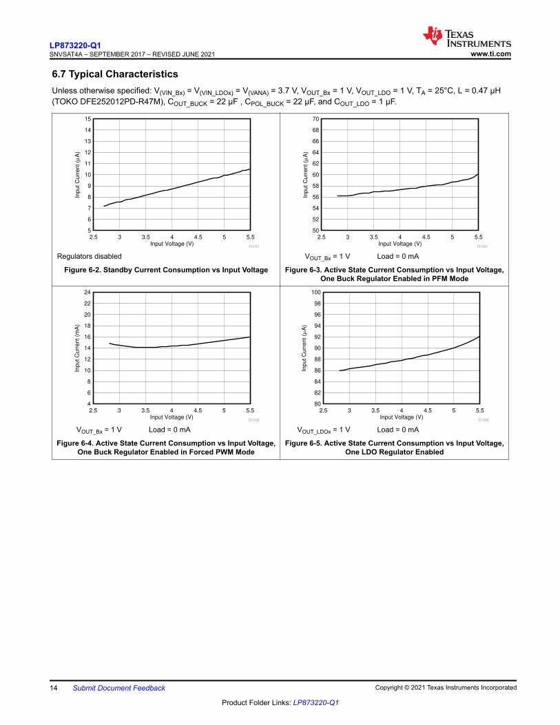
6.7 Typical CharacteristicsUnless otherwise specified: V(VIN_Bx) = V(VIN_LDOx) = V(VANA) = 3.7 V, VOUT_Bx = 1 V, VOUT_LDO = 1 V, TA = 25°C, L = 0.47 µH (TOKO DFE252012PD-R47M), COUT_BUCK = 22 µF , CPOL_BUCK = 22 µF, and COUT_LDO = 1 µF.
Input Voltage (V)
Inp
ut
Cu
rren
t (P
A)
2.5 3 3.5 4 4.5 5 5.55
6
7
8
9
10
11
12
13
14
15
D101
Regulators disabled
Figure 6-2. Standby Current Consumption vs Input Voltage
Input Voltage (V)
Inp
ut
Cu
rren
t (P
A)
2.5 3 3.5 4 4.5 5 5.550
52
54
56
58
60
62
64
66
68
70
D102
VOUT_Bx = 1 V Load = 0 mA
Figure 6-3. Active State Current Consumption vs Input Voltage, One Buck Regulator Enabled in PFM Mode
Input Voltage (V)
Inp
ut
Cu
rren
t (m
A)
2.5 3 3.5 4 4.5 5 5.54
6
8
10
12
14
16
18
20
22
24
D103
VOUT_Bx = 1 V Load = 0 mA
Figure 6-4. Active State Current Consumption vs Input Voltage, One Buck Regulator Enabled in Forced PWM Mode
Input Voltage (V)
Input
Curr
ent
(PA
)
2.5 3 3.5 4 4.5 5 5.580
82
84
86
88
90
92
94
96
98
100
D104
VOUT_LDOx = 1 V Load = 0 mA
Figure 6-5. Active State Current Consumption vs Input Voltage, One LDO Regulator Enabled
LP873220-Q1SNVSAT4A – SEPTEMBER 2017 – REVISED JUNE 2021 www.ti.com
14 Submit Document Feedback Copyright © 2021 Texas Instruments Incorporated
Product Folder Links: LP873220-Q1

7 Detailed Description7.1 OverviewThe LP873220-Q1 is a high-efficiency, high-performance flexible power supply device with two step-down DC/DC converter cores (Buck0 and Buck1) and two low-dropout (LDO) linear regulators (LDO0 and LDO1) for automotive applications. Table 7-1 lists the output characteristics of the regulators.
Table 7-1. Supply Specification
SUPPLYOUTPUTVOUT RANGE (V) RESOLUTION (mV) IMAX MAXIMUM OUTPUT CURRENT (mA)
Buck0 0.7 to 3.3610 (0.7 V to 0.73 V)5 (0.73 V to 1.4 V)20 (1.4 V to 3.36 V)
2000
Buck1 0.7 to 3.3610 (0.7 V to 0.73 V)5 (0.73 V to 1.4 V)20 (1.4 V to 3.36 V)
2000
LDO0 0.8 to 3.3 100 300
LDO1 0.8 to 3.3 100 300
The LP873220-Q1 also supports switching clock synchronization to an external clock (CLKIN pin). The nominal frequency of the external clock can be from 1 MHz to 24 MHz with 1-MHz steps.
Additional features include:• Soft-start• Input voltage protection:
– Undervoltage lockout– Overvoltage protection
• Output voltage monitoring and protection:– Overvoltage monitoring– Undervoltage monitoring– Overload protection
• Thermal warning• Thermal shutdown
The LP873220-Q1 has one dedicated general purpose digital output (GPO) signal. The CLKIN pin can be programmed as a second GPO signal (GPO2), if the external clock is not needed. The output type (open-drain or push-pull) is programmable for the GPOs.
www.ti.comLP873220-Q1
SNVSAT4A – SEPTEMBER 2017 – REVISED JUNE 2021
Copyright © 2021 Texas Instruments Incorporated Submit Document Feedback 15
Product Folder Links: LP873220-Q1

7.2 Functional Block Diagram
UVLO
SWReset
DigitalLogic
Registers
I2C
Enable and Disable,
Delay
ControlSlew-Rate
Control
Interrupts
nINT
SDASCL
EN
VANA
OTP EPROM
Thermal Monitor
Oscillator
Buck0
ILIM Det
Pwrgood Det
Overload and SC Det
Buck1
LDO0
LDO1
ILIM DetPwrgood Det
Overload and
SC Det
ILIM DetPwrgood Det
Overload
and SC Det
ILIM DetPwrgood Det
Overload and SC Det
Ref &
Bias
Iload ADC
Iload ADC
CLKIN (GPO2)
PGOOD
GPO
Copyright © 2016, Texas Instruments Incorporated
7.3 Feature Description7.3.1 DC/DC Converters7.3.1.1 Overview
The LP873220-Q1 includes two step-down DC/DC converter cores. The cores are designed for flexibility; most of the functions are programmable, thus giving a possibility to optimize the regulator operation for each application. The buck regulators deliver 0.7-V to 3.36-V regulated voltage rails from a 2.8-V to 5.5-V supply voltage.
The LP873220-Q1 has the following features:
• DVS support with programmable slew rate• Automatic mode control based on the loading (PFM or PWM mode)• Forced PWM mode option• Optional external clock input to minimize crosstalk• Optional spread-spectrum technique to reduce EMI• Phase control for optimized EMI• Synchronous rectification• Current mode loop with PI compensator• Soft start• Power Good flag with maskable interrupt• Power Good signal (PGOOD) with selectable sources• Average output current sensing (for PFM entry and load current measurement)
LP873220-Q1SNVSAT4A – SEPTEMBER 2017 – REVISED JUNE 2021 www.ti.com
16 Submit Document Feedback Copyright © 2021 Texas Instruments Incorporated
Product Folder Links: LP873220-Q1

The following parameters can be programmed through the registers, the default values are set by OTP bits:
• Output voltage• Forced PWM operation• Switch current limit• Output voltage slew rate• Enable and disable delays
There are two modes of operation for the buck converter, depending on the output current required: pulse-width modulation (PWM) and pulse-frequency modulation (PFM). The converter operates in PWM mode at high load currents of approximately 600 mA or higher. Lighter output current loads cause the converter to automatically switch into PFM mode for reduced current consumption when forced PWM mode is disabled. The forced PWM mode can be selected to maintain fixed switching frequency at all load current levels.
A block diagram of a single core is shown in Figure 7-1.
FB
+
-
+-
POWER GOOD
LOOPCOMP
RAMPGENERATOR
HS FETCURRENT
SENSE
LS FETCURRENT
SENSE
GATECONTROL
IADC
VDAC
ERRORAMP
GND
NEG CURRENT
LIMIT
ZERO CROSS
DETECT
SW
-+
POS CURRENT
LIMIT
VIN
VOUT
CONTROLBLOCK
PROGRAMMABLE PARAMETERS
SLAVE INTERFACE
VOLTAGE SETTING
SLEW RATE
CONTROLMASTER
INTERFACE
Copyright © 2016, Texas Instruments Incorporated
Figure 7-1. Detailed Block Diagram Showing One Core
7.3.1.2 Transition Between PWM and PFM Modes
The PWM mode operation optimizes efficiency at mid to full load at the expense of light-load efficiency. The LP873220-Q1 converter operates in the PWM mode at load current of about 600 mA or higher. At lighter load current levels the device automatically switches into the PFM mode for reduced current consumption when forced PWM mode is disabled (AUTO mode operation). By combining the PFM and the PWM modes, a high efficiency is achieved over a wide output-load current range.
7.3.1.3 Buck Converter Load Current Measurement
The buck load current can be monitored through I2C registers. The monitored buck converter is selected with the LOAD_CURRENT_BUCK_SELECT bit in the SEL_I_LOAD register. A write to this selection register starts a current measurement sequence. The regulator is automatically forced to the PWM mode for the measurement period. The measurement sequence is 50 µs long, maximum.
The LP873220-Q1 device can be configured to give out an interrupt (the I_MEAS_INT bit in the INT_TOP_1 register) after the load current measurement sequence is finished. The load current measurement interrupt can be masked with the I_MEAS_MASK bit (TOP_MASK_1 register). The measurement result can be read from the registers I_LOAD_1 and I_LOAD_2. The register I_LOAD_1 bits BUCK_LOAD_CURRENT[7:0] gives out the LSB bits, and the register I_LOAD_2 bit BUCK_LOAD_CURRENT[8] gives out the MSB bit. The measurement result BUCK_LOAD_CURRENT[8:0] LSB is 20 mA, and the maximum code value of the measurement corresponds to 10.22 A.
www.ti.comLP873220-Q1
SNVSAT4A – SEPTEMBER 2017 – REVISED JUNE 2021
Copyright © 2021 Texas Instruments Incorporated Submit Document Feedback 17
Product Folder Links: LP873220-Q1

7.3.1.4 Spread-Spectrum Mode
Systems with periodic switching signals may generate a large amount of switching noise in a set of narrowband frequencies (the switching frequency and its harmonics). The usual solution to reduce noise coupling is to add EMI-filters and shields to the boards. The LP873220-Q1 has a register-selectable spread-spectrum mode which minimizes the need for output filters, ferrite beads, or chokes. In spread spectrum mode, the switching frequency varies around the center frequency, reducing the EMI emissions radiated by the converter and associated passive components and PCB traces (see Figure 7-2). Spread-spectrum mode is only available when an internal RC oscillator is used (EN_PLL bit is 0 in PLL_CTRL register), it is enabled with the EN_SPREAD_SPEC bit in the CONFIG register, and it affects both buck cores.
Po
we
r S
pe
ctr
um
is
Sp
rea
d a
nd
Lo
we
red
Frequency
Ra
dia
ted
En
erg
y
Where a fixed frequency converter exhibits large amounts of spectral energy at the switching frequency, the spread spectrum architecture of the LP873220-Q1 spreads that energy over a large bandwidth.
Figure 7-2. Spread-Spectrum Modulation
7.3.2 Sync Clock Functionality
The LP873220-Q1 device contains a CLKIN input to synchronize the switching clock of the buck regulators with the external clock. The block diagram of the clocking and PLL module is shown in Figure 7-3. Depending on the EN_PLL bit in the PLL_CTRL register and the external clock availability, the external clock is selected and interrupt is generated as shown in Table 7-2. The interrupt can be masked with the SYNC_CLK_MASK bit in the TOP_MASK_1 register. The nominal frequency of the external input clock is set by the EXT_CLK_FREQ[4:0] bits in the PLL_CTRL register, and it can be from 1 MHz to 24 MHz with 1-MHz steps. The external clock must be inside accuracy limits (–30%/+10%) of the selected frequency for valid clock detection.
The SYNC_CLK_INT interrupt in the INT_TOP_1 register is also generated in cases where the external clock is expected but is not available. These cases occur when EN_PLL is 1 during start-up (read OTP-to-standby transition) and during Buck regulator enable (standby-to-active transition).
LP873220-Q1SNVSAT4A – SEPTEMBER 2017 – REVISED JUNE 2021 www.ti.com
18 Submit Document Feedback Copyright © 2021 Texas Instruments Incorporated
Product Folder Links: LP873220-Q1

24 MHz
RC
Oscillator
CLKIN
Divider
´(;7_CLK
_)5(4´ PLL
Divider
24
CLKIN
Detector
Clock Select
Logic
Internal
24 MHz
clock
1 MHz
1 MHz
´(1_3//´
24 MHz
Figure 7-3. Clock and PLL Module
Table 7-2. PLL OperationDEVICE OPERATION MODE EN_PLL PLL AND CLOCK
DETECTOR STATEINTERRUPT FOR EXTERNAL CLOCK CLOCK
STANDBY 0 Disabled No Internal RC
ACTIVE 0 Disabled No Internal RC
STANDBY 1 Enabled When external clock appears or disappears
Automatic change to external clock when available
ACTIVE 1 Enabled When external clock appears or disappears
Automatic change to external clock when available
7.3.3 Low-Dropout Linear Regulators (LDOs)
The LP873220-Q1 device includes two identical linear regulators, LDO0 and LDO1, which target analog loads with low noise requirements. The LDO regulators deliver 0.8-V to 3.3-V regulated voltage rails from a 2.5-V to 5.5-V input voltage. Both regulators have dedicated inputs which can be higher or lower than the device system voltage V(VANA) to minimize the power dissipation.
7.3.4 Power-Up
The power-up sequence for the LP873220-Q1 is as follows:
• The VANA and VIN_Bx reach minimum recommended levels (VVANA > VANAUVLO). This initiates power-on-reset (POR), OTP reading, and enables the system I/O interface. The I2C host should allow at least 1.2 ms before writing or reading data to the LP873220-Q1.
• The device enters standby mode.• The host can change the default register setting by I2C if needed.• The regulators can be enabled and disabled.• The GPO signals can be controlled by the EN pin and the I2C interface.
Transitions between the operating modes are shown in Section 7.4.1.
www.ti.comLP873220-Q1
SNVSAT4A – SEPTEMBER 2017 – REVISED JUNE 2021
Copyright © 2021 Texas Instruments Incorporated Submit Document Feedback 19
Product Folder Links: LP873220-Q1

7.3.5 Regulator Control7.3.5.1 Enabling and Disabling Regulators
The regulators can be enabled when the device is in STANDBY or ACTIVE state. There are two ways to enable and disable the buck regulators:• Using the BUCKx_EN bit in the BUCKx_CTRL_1 register (the BUCKx_EN_PIN_CTRL bit is 0 in the
BUCKx_CTRL_1 register).• Using the EN control pin (the BUCKx_EN bit and the BUCKx_EN_PIN_CTRL bit is 1).
Similarly, there are two ways to enable and disable the LDO regulators:• Using the LDOx_EN bit in the LDOx_CTRL register (the LDOx_EN_PIN_CTRL bit is 0 in the LDOx_CTRL
register).• Using the EN control pin (the LDOx_EN bit is 1 and the LDOx_EN_PIN_CTRL bit is 1).
If the EN control pin is used for enable and disable, then the following occurs:
• The delay from the control signal rising edge to start-up is set by the BUCKx_STARTUP_DELAY[3:0] bits in the BUCKx_DELAY register and the LDOx_STARTUP_DELAY[3:0] bits in the LDOx_DELAY register.
• The delay from the control signal falling edge to shutdown is set by the BUCKx_SHUTDOWN_DELAY[3:0] bits in the BUCKx_DELAY register and the LDOx_SHUTDOWN_DELAY[3:0] bits in the LDOx_DELAY register.
The delays are only valid for the EN signal transitions and not for control with I2C writings to the BUCKx_EN and the LDOx_EN bits.
The control of the regulator (with 0-ms delays) is shown in Table 7-3.
Table 7-3. Regulator ControlBUCKx_EN AND
LDOx_ENBUCKx_EN_PIN_CTRL AND
LDOx_EN_PIN_CTRL EN PIN BUCKx OUTPUT VOLTAGE ANDLDOx OUTPUT VOLTAGE
Enable and disable control with the BUCKx_EN and the
LDOx_EN bit
0 Don't Care Don't Care Disabled
1 0 Don't Care BUCKx_VSET[7:0] and LDOx_VSET[4:0]
Enable and disable control with the EN pin
1 1 Low Disabled
1 1 High BUCKx_VSET[7:0] and LDOx_VSET[4:0]
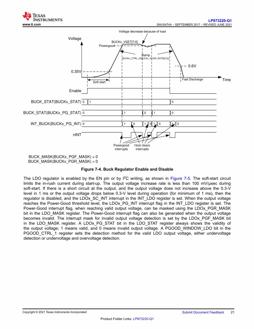
The buck regulator is enabled by the EN pin or by I2C writing as shown in Figure 7-4. The soft-start circuit limits the in-rush current during start-up. When the output voltage rises to a 0.35-V level, the output voltage becomes slew-rate controlled. If there is a short circuit at the output, and the output voltage does not increase above the 0.35-V level in 1 ms or the output voltage drops below 0.35-V level during operation (for minimum of 1 ms), then the regulator is disabled, and the BUCKx_SC_INT interrupt in the INT_BUCK register is set. When the output voltage reaches the Power-Good threshold level, the BUCKx_PG_INT interrupt flag in the INT_BUCK register is set. The Power-Good interrupt flag, when reaching valid output voltage, can be masked using the BUCKx_PGR_MASK bit in the BUCK_MASK register. The Power-Good interrupt flag can also be generated when the output voltage becomes invalid. The interrupt mask for invalid output voltage detection is set by the BUCKx_PGF_MASK bit in the BUCK_MASK register. A BUCKx_PG_STAT bit in the BUCK_STAT register always shows the validity of the output voltage; 1 means valid and 0 means invalid output voltage. A PGOOD_WINDOW_BUCK bit in the PGOOD_CTRL_1 register sets the detection method for the valid buck output voltage, either undervoltage detection or undervoltage and overvoltage detection.
LP873220-Q1SNVSAT4A – SEPTEMBER 2017 – REVISED JUNE 2021 www.ti.com
20 Submit Document Feedback Copyright © 2021 Texas Instruments Incorporated
Product Folder Links: LP873220-Q1
0.6V
Enable
Time
Voltage
Soft start
RampBUCKx_CTRL_2(BUCKx_SLEW_RATE[2:0])
Fast Discharge
BUCKx_VSET[7:0]
INT_BUCK(BUCKx_PG_INT)
nINT
Powergood
BUCK_STAT(BUCKx_PG_STAT)
0.35V
Voltage decrease because of load
BUCK_STAT(BUCKx_STAT)
BUCK_MASK(BUCKx_PGF_MASK) = 0
BUCK_MASK(BUCKx_PGR_MASK) = 0
Host clears
interrupts
Powergood
interrupts
00 1
00 1
0 1
10 0 1 0 1 0 1 0
Figure 7-4. Buck Regulator Enable and Disable
The LDO regulator is enabled by the EN pin or by I2C writing, as shown in Figure 7-5. The soft-start circuit limits the in-rush current during start-up. The output voltage increase rate is less than 100 mV/μsec during soft-start. If there is a short circuit at the output, and the output voltage does not increase above the 0.3-V level in 1 ms or the output voltage drops below 0.3-V level during operation (for minimum of 1 ms), then the regulator is disabled, and the LDOx_SC_INT interrupt in the INT_LDO register is set. When the output voltage reaches the Power-Good threshold level, the LDOx_PG_INT interrupt flag in the INT_LDO register is set. The Power-Good interrupt flag, when reaching valid output voltage, can be masked using the LDOx_PGR_MASK bit in the LDO_MASK register. The Power-Good interrupt flag can also be generated when the output voltage becomes invalid. The interrupt mask for invalid output voltage detection is set by the LDOx_PGF_MASK bit in the LDO_MASK register. A LDOx_PG_STAT bit in the LDO_STAT register always shows the validity of the output voltage; 1 means valid, and 0 means invalid output voltage. A PGOOD_WINDOW_LDO bit in the PGOOD_CTRL_1 register sets the detection method for the valid LDO output voltage, either undervoltage detection or undervoltage and overvoltage detection.
www.ti.comLP873220-Q1
SNVSAT4A – SEPTEMBER 2017 – REVISED JUNE 2021
Copyright © 2021 Texas Instruments Incorporated Submit Document Feedback 21
Product Folder Links: LP873220-Q1

Enable
Time
Voltage
Resistive pull-down
(if enabled)
LDOx_VSET[4:0]
INT_LDO(LDOx_PG_INT)
nINT
Host clears
interrupts
Powergood
interrupts
Powergood
LDO_STAT(LDOx_PG_STAT) 00 1
Voltage decrease because of load
LDO_STAT(LDOx_STAT) 00 1
0 1
10 0 1 0 1 0
LDO_MASK(LDOx_PGF_MASK) = 0
LDO_MASK(LDOx_PGR_MASK) = 0
1 0
Figure 7-5. LDO Regulator Enable and Disable
The EN input pin has an integrated pulldown resistor. The pulldown resistor is controlled with the EN_PD bit in the CONFIG register.
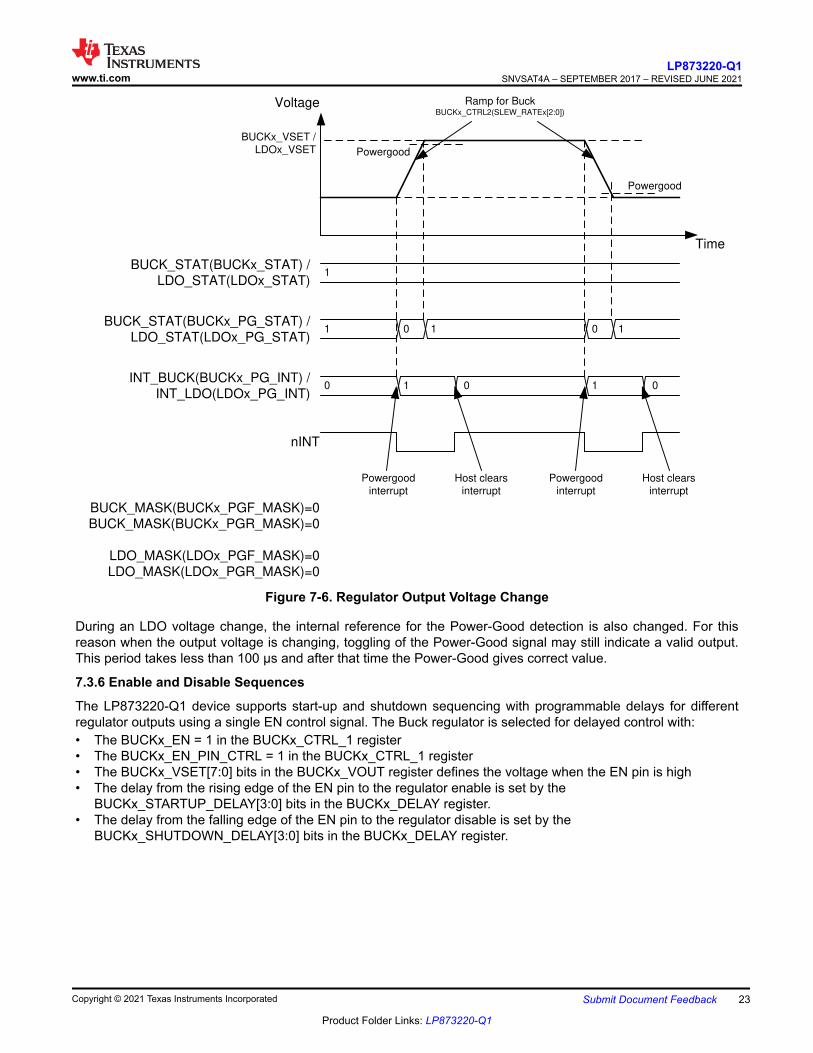
7.3.5.2 Changing Output Voltage
The output voltage of the regulator can be changed by writing to the BUCKx_VOUT and LDOx_VOUT register. The voltage change for the buck regulator is always slew-rate controlled, and the slew-rate is defined by the BUCKx_SLEW_RATE[2:0] bits in the BUCKx_CTRL_2 register. During voltage change, the forced PWM mode is used automatically. When the programmed output voltage is achieved, the mode becomes the one defined by the load current, the BUCKx_FPWM bit in the BUCKx_CTRL_1 register.
The voltage change and Power-Good interrupts are shown in Figure 7-6.
LP873220-Q1SNVSAT4A – SEPTEMBER 2017 – REVISED JUNE 2021 www.ti.com
22 Submit Document Feedback Copyright © 2021 Texas Instruments Incorporated
Product Folder Links: LP873220-Q1
Time
Voltage Ramp for BuckBUCKx_CTRL2(SLEW_RATEx[2:0])
BUCKx_VSET /
LDOx_VSET
INT_BUCK(BUCKx_PG_INT) /
INT_LDO(LDOx_PG_INT)
nINT
Host clears
interrupt
Powergood
interrupt
Powergood
BUCK_STAT(BUCKx_STAT) /
LDO_STAT(LDOx_STAT)1
Powergood
BUCK_STAT(BUCKx_PG_STAT) /
LDO_STAT(LDOx_PG_STAT)
Host clears
interrupt
Powergood
interrupt
1 0 1 0 1
0 1 0 1 0
BUCK_MASK(BUCKx_PGF_MASK)=0
BUCK_MASK(BUCKx_PGR_MASK)=0
LDO_MASK(LDOx_PGF_MASK)=0
LDO_MASK(LDOx_PGR_MASK)=0
Figure 7-6. Regulator Output Voltage Change
During an LDO voltage change, the internal reference for the Power-Good detection is also changed. For this reason when the output voltage is changing, toggling of the Power-Good signal may still indicate a valid output. This period takes less than 100 µs and after that time the Power-Good gives correct value.
7.3.6 Enable and Disable Sequences
The LP873220-Q1 device supports start-up and shutdown sequencing with programmable delays for different regulator outputs using a single EN control signal. The Buck regulator is selected for delayed control with:• The BUCKx_EN = 1 in the BUCKx_CTRL_1 register• The BUCKx_EN_PIN_CTRL = 1 in the BUCKx_CTRL_1 register• The BUCKx_VSET[7:0] bits in the BUCKx_VOUT register defines the voltage when the EN pin is high• The delay from the rising edge of the EN pin to the regulator enable is set by the
BUCKx_STARTUP_DELAY[3:0] bits in the BUCKx_DELAY register.• The delay from the falling edge of the EN pin to the regulator disable is set by the
BUCKx_SHUTDOWN_DELAY[3:0] bits in the BUCKx_DELAY register.
www.ti.comLP873220-Q1
SNVSAT4A – SEPTEMBER 2017 – REVISED JUNE 2021
Copyright © 2021 Texas Instruments Incorporated Submit Document Feedback 23
Product Folder Links: LP873220-Q1

In the same way, the LDO regulator is selected for delayed control with:• The LDOx_EN = 1 in the LDOx_CTRL register• The LDOx_EN_PIN_CTRL = 1 in the LDOx_CTRL register• The LDOx_VSET[4:0] bits in the LDOx_VOUT register defines the voltage when the EN pin is high• The delay from the rising edge of the EN pin to the regulator enable is set by the
LDOx_STARTUP_DELAY[3:0] bits in the LDOx_DELAY register.• The delay from the falling edge of the EN pin to the regulator disable is set by the
LDOx_SHUTDOWN_DELAY[3:0] bits in the LDOx_DELAY register.
The GPO and GPO2 digital output signals can be also controlled as a part of start-up and shutdown sequencing with the following settings:• GPOx_EN = 1 in GPO_CTRL register• GPOx_EN_PIN_CTRL = 1 in GPO_CTRL register• The delay from the rising edge of the EN pin to the rising edge of the GPO or GPO2 signal is set by the
GPOx_STARTUP_DELAY[3:0] bits in the GPOx_DELAY register.• The delay from the falling edge of the EN pin to the falling edge of the GPO or GPO2 signal is set by the
GPOx_SHUTDOWN_DELAY[3:0] bits in the GPOx_DELAY register.
An example of the start-up and shutdown sequences for the buck regulators are shown in Figure 7-7. The start-up and shutdown delays for the Buck0 regulator are 1 ms and 4 ms, and for the Buck1 regulator the start-up and shutdown delays are 3 ms and 1 ms. The delay settings are only used for enable or disable control with the EN signal.
EN
EN_BUCK0
EN
1 ms
3 msEN_BUCK1 1 ms
4 ms
EN_BUCK0
EN_BUCK1 3 ms
1 ms
1 ms
4 ms
Typical sequence
Sequence with short EN low and high periods
Startup cntr
Shutdown cntr
0 0 1
0 0 1
0 1 2 3 4 5 6 0
0 1 2 0 1 2 3 4 5
Figure 7-7. Start-Up and Shutdown Sequencing
LP873220-Q1SNVSAT4A – SEPTEMBER 2017 – REVISED JUNE 2021 www.ti.com
24 Submit Document Feedback Copyright © 2021 Texas Instruments Incorporated
Product Folder Links: LP873220-Q1

7.3.7 Device Reset Scenarios
There are two reset methods implemented on the LP873220-Q1:
• Software reset with the SW_RESET bit in the RESET register.• Undervoltage lockout (UVLO) reset from the VANA supply.
An software reset occurs when 1 is written to the SW_RESET bit. The bit is automatically cleared after writing. This event disables all the regulators immediately, drives the GPO or GPO2 signals low, resets all the register bits to the default values, and loads the OTP bits (see Figure 7-13). The I2C interface is not reset during a software reset.
If the VANA supply voltage falls below the UVLO threshold level, then all the regulators are disabled immediately, the GPO or GPO2 signals are driven low, and all the register bits are reset to the default values. When the VANA supply voltage transitions above the UVLO threshold level, an internal POR occurs. The OTP bits are loaded to the registers and a startup is initiated according to the register settings.
7.3.8 Diagnosis and Protection Features
The LP873220-Q1 is capable of providing four levels of protection features:• Information of valid regulator output voltage, which sets the interrupt or PGOOD signal.• Warnings for diagnosis, which sets the interrupt.• Protection events, which are disabling the regulators.• Faults, which are causing the device to shutdown.
The LP873220-Q1 sets the flag bits indicating what protection or warning conditions have occurred, and the nINT pin is pulled low. The nINT is released again after a clear of flags is complete. The nINT signal stays low until all the pending interrupts are cleared.
When a fault is detected or software requested reset, it is indicated by a RESET_REG_INT interrupt flag in the INT_TOP_2 register after next start-up. If the RESET_REG_MASK is set to masked in the OTP, then the interrupt is not generated. The mask bit change with I2C does not affect, because the RESET_REG_MASK bit is loaded from the OTP during reset sequence.
www.ti.comLP873220-Q1
SNVSAT4A – SEPTEMBER 2017 – REVISED JUNE 2021
Copyright © 2021 Texas Instruments Incorporated Submit Document Feedback 25
Product Folder Links: LP873220-Q1

Table 7-4. Summary of Interrupt SignalsEVENT DEVICE RESPONSE INTERRUPT BIT INTERRUPT MASK BIT STATUS BIT RECOVERY AND INTERRUPT
CLEAR
Buck current limit triggered No effect BUCK_INTBUCKx_ILIM_INT BUCKx_ILIM_MASK BUCKx_ILIM_STAT
Write 1 to the BUCKx_ILIM_INT bit.Interrupt is not cleared if the current limit is active
LDO current limit triggered No effect LDO_INTLDOx_ILIM_INT LDOx_ILIM_MASK LDOx_ILIM_STAT
Write 1 to the LDOx_ILIM_INT bitInterrupt is not cleared if the current limit is active
Buck short circuit (VVOUT < 0.35 V at 1 ms after enable) or overload (VVOUT decreasing below 0.35 V during operation, 1-ms debounce)
Regulator disable BUCK_INTBUCKx_SC_INT N/A N/A Write 1 to the BUCKx_SC_INT bit
LDO short circuit (VVOUT < 0.3 V at 1 ms after enable) or overload (VVOUT decreasing below 0.3 V during operation, 1-ms debounce)
Regulator disable LDO_INTLDOx_SC_INT N/A N/A Write 1 to the LDOx_SC_INT bit
Thermal warning No effect TDIE_WARN_INT TDIE_WARN_MASK TDIE_WARN_STAT
Write 1 to tge TDIE_WARN_INT bitInterrupt is not cleared if the temperature is above the thermal warning level
Thermal shutdown
All the regulators are disabled immediately, and the GPO and GPO2 are set to low
TDIE_SD_INT N/A TDIE_SD_STAT
Write 1 to the TDIE_SD_INT bitInterrupt is not cleared if the temperature is above the thermal shutdown level
VANA overvoltage (VANAOVP)
All the regulators are disabled immediately, and the GPO and GPO2 are set to low
OVP_INT N/A OVP_STAT
Write 1 to the OVP_INT bitInterrupt is not cleared if the VANA voltage is above the VANAOVP level
Buck power good, output voltage becomes valid No effect BUCK_INT
BUCKx_PG_INT BUCKx_PGR_MASK BUCKx_PG_STAT Write 1 to the BUCKx_PG_INT bit
Buck power good, output voltage becomes invalid No effect BUCK_INT
BUCKx_PG_INT BUCKx_PGF_MASK BUCKx_PG_STAT Write 1 to the BUCKx_PG_INT bit
LDO Power good, output voltage becomes valid No effect LDO_INT
LDOx_PG_INT LDOx_PGR_MASK LDOx_PG_STAT Write 1 to the LDOx_PG_INT bit
LDO power good, output voltage becomes invalid No effect LDO_INT
LDOx_PG_INT LDOx_PGF_MASK LDOx_PG_STAT Write 1 to the LDOx_PG_INT bit
PGOOD pin changing from active to inactive state(1) No effect PGOOD_INT PGOOD_MASK PGOOD_STAT Write 1 to the PGOOD_INT bit
External clock appears or disappears No effect to regulators SYNC_CLK_INT(2) SYNC_CLK_MASK SYNC_CLK_STAT Write 1 to the SYNC_CLK_INT bit
Load current measurement is ready No effect I_MEAS_INT I_MEAS_MASK N/A Write 1 to the I_MEAS_INT bit
Supply voltage VANAUVLO triggered (VANA falling)
Immediate shutdown and the registers reset to default values
N/A N/A N/A N/A
Supply voltage VANAUVLO triggered (VANA rising)
Startup and the registers reset to default values and the OTP bits are loaded
RESET_REG_INT RESET_REG_MASK N/A Write 1 to the RESET_REG_INT bit
Software requested reset
Immediate shutdown is followed by power up and the registers are reset to their default values
RESET_REG_INT RESET_REG_MASK N/A Write 1 to the RESET_REG_INT bit
(1) The PGOOD_STAT bit is 1 when the PGOOD pin shows valid voltages. The PGOOD_POL bit in the PGOOD_CTRL_1 register affects only the PGOOD pin polarity, not the Power Good and PGOOD_INT interrupt polarity.
(2) If the clock is not available when the clock detector is enabled, then an interrupt is generated during the clock-dector operation.
LP873220-Q1SNVSAT4A – SEPTEMBER 2017 – REVISED JUNE 2021 www.ti.com
26 Submit Document Feedback Copyright © 2021 Texas Instruments Incorporated
Product Folder Links: LP873220-Q1

7.3.8.1 Power-Good Information (PGOOD pin)
In addition to the interrupt-based indication of the current limit and the Power-Good level, the LP873220-Q1 device supports monitoring with PGOOD signal:• Regulator output voltage• Input supply overvoltage• Thermal warning• Thermal shutdown
The regulator output voltage monitoring (not current limit monitoring) can be selected for the PGOOD indication. This selection is individual for both buck regulators and LDO regulators, and is set by the EN_PGOOD_BUCKx bits in the PGOOD_CTRL_1 register and the EN_PGOOD_LDOx bits in the PGOOD_CTRL_1 register. When a regulator is disabled, the monitoring is automatically masked to prevent it forcing the PGOOD inactive. A thermal warning can also be selected for the PGOOD indication with the EN_PGOOD_TWARN bit in the PGOOD_CTRL_2 register. The monitoring from all the output rails, thermal warning (TDIE_WARN_STAT), input overvoltage interrupt (OVP_INT), and thermal shutdown interrupt (TDIE_SD_INT) are combined, and the PGOOD pin is active only if all the selected sources shows a valid status.
The type of output voltage monitoring for the PGOOD signal is selected by the PGOOD_WINDOW_x bits in the PGOOD_CTRL_1 register. If the bit is 0, only undervoltage is monitored; if the bit is 1, both undervoltage and overvoltage are monitored.
The polarity and the output type (push-pull or open-drain) are selected by the PGOOD_POL and PGOOD_OD bits in the PGOOD_CTRL_1 register.
The PGOOD is only active and asserted when all enabled power resource output voltages are within specified tolerance for each requested and programmed output voltage.
The PGOOD is inactive and de-asserted if any enabled power resource output voltages is outside specified tolerance for each requested and programmed output voltage.
The device OTP setting selects either gated (or unusual) or continuous (or invalid) mode of operation.
7.3.8.1.1 PGOOD Pin Gated Mode
The gated (or unusual) mode of operation is selected by setting the PGOOD_MODE bit to 0 in the PGOOD_CTRL_2 register.
For the gated mode of operation, the PGOOD behaves as follows:• PGOOD is set to active or asserted state upon exiting the OTP configuration as an initial default state.• PGOOD status is suspended or unchanged during an 800-µs gated time period, thereby gating-off the status
indication.• During normal power-up sequencing and requested voltage changes, the PGOOD state is not changed
during an 800-µs gated time period. It typically remains active or asserted for normal conditions.• During an abnormal power-up sequencing and requested voltage changes, the PGOOD status could change
to inactive or de-asserted after an 800-µs gated time period if any output voltage is outside of regulation range.
• Using the gated mode of operation could allow the PGOOD signal to initiate an immediate power shutdown sequence if the PGOOD signal is wired-OR with signal connected to the EN input. This type of circuit configuration provides a smart PORz function for processor that eliminates the need for additional components to generate PORz upon start-up and to monitor voltage levels of key voltage domains.
Each detected fault sets the correcting fault bit in the PG_FAULT register to 1. The detected fault must be cleared to continue the PGOOD monitoring. The overvoltage and thermal shutdown are cleared by writing 1 to the OVP_INT and TDIE_SD_INT interrupt bits in the INT_TOP_1 register. The regulator fault is cleared by writing 1 to the corresponding register bit in the PG_FAULT register. The interrupts can also be cleared with the VANA UVLO by toggling the input supply. An example of the PGOOD pin operation in gated mode is shown in Figure 7-8.
www.ti.comLP873220-Q1
SNVSAT4A – SEPTEMBER 2017 – REVISED JUNE 2021
Copyright © 2021 Texas Instruments Incorporated Submit Document Feedback 27
Product Folder Links: LP873220-Q1

V(VANA)
VANA_UVLO
State ShutdownRead OTP
Standby
PGOOD pin
EN pin
VOUT (Buck1)
VOUT (LDO0)
Buck1 internal powergood
LDO0 internal powergood
Active
800 µs Timer
Buck internal enable
800 µs Timer
LDO0 internal enable
4 ms
2 ms
Clear fault
Figure 7-8. PGOOD Pin Operation in Gated Mode
7.3.8.1.2 PGOOD Pin Continuous Mode
The continuous (or invalid) mode of operation is selected by setting the PGOOD_MODE bit to 1 in the PGOOD_CTRL_2 register.
For the continuous mode of operation, PGOOD behaves as follows:• PGOOD is set to active or asserted state upon exiting OTP configuration.• PGOOD is set to inactive or de-asserted as soon as the regulator is enabled.• PGOOD status begins indicating output voltage regulation status immediately and continuously.• During power-up sequencing and requested voltage changes, PGOOD will toggle between inactive or
de-asserted while output voltages are outside of regulation ranges and active or asserted when inside of regulation ranges.
The PG_FAULT register bits are latched, and maintain the fault information until the host clears the fault bit by writing 1 to the bit. The PGOOD signal also indicates a thermal shutdown and input overvoltage interrupts, which are cleared by clearing the interrupt bits.
When the regulator voltage is transitioning from one target voltage to another, the PGOOD signal becomes inactive.
7.3.8.1.3 PGOOD Pin Inactive Mode
When the PGOOD signal becomes inactive, the source for the fault can be read from the PG_FAULT register. If the invalid output voltage becomes valid again, then the PGOOD signal becomes active. Thus the PGOOD signal always shows if the monitored output voltages are valid. The block diagram for this operation is shown in Figure 7-9 and an example of operation is shown in Figure 7-10.
The PGOOD signal can also be configured so that it maintains an inactive state even when the monitored outputs are valid, but there are PG_FAULT_x bits in the PG_FAULT register pending clearance. This type of operation is selected by setting the PGFAULT_GATES_PGOOD bit to 1 in the PGOOD_CTRL_2 register.
LP873220-Q1SNVSAT4A – SEPTEMBER 2017 – REVISED JUNE 2021 www.ti.com
28 Submit Document Feedback Copyright © 2021 Texas Instruments Incorporated
Product Folder Links: LP873220-Q1

Buck0Power Good
EN_PGOOD
_BUCK0
Buck1
PGOOD
Active High
EN_PGOOD
_BUCK1
LDO0
EN_PGOOD
_LDO0
LDO1
EN_PGOOD
_LDO1
TDIE_SD_INT
OVP_INT
Power Good
Power Good
Power Good
Copyright © 2016, Texas Instruments Incorporated
TDIE_WARN_STAT
EN_PGOOD
_TWARN
Figure 7-9. PGOOD Block Diagram (Continuous Mode)
V(VANA)
VANA_UVLO
State ShutdownRead
OTPStandby
PGOOD pin
EN pin
VOUT (Buck1)
VOUT (LDO0)
Buck1 internal powergood
LDO0 internal powergood
Active
Buck1 internal enable
LDO0 internal enable
4 ms
2 ms
Figure 7-10. PGOOD Pin Operation in Continuous Mode
www.ti.comLP873220-Q1
SNVSAT4A – SEPTEMBER 2017 – REVISED JUNE 2021
Copyright © 2021 Texas Instruments Incorporated Submit Document Feedback 29
Product Folder Links: LP873220-Q1

7.3.8.2 Warnings for Diagnosis (Interrupt)7.3.8.2.1 Output Power Limit
The Buck regulators have programmable output peak current limits. The limits are individually programmed for both regulators with the BUCKx_ILIM[2:0] bits in the BUCKx_CTRL_2 register. If the load current is increased so that the current limit is triggered, then the regulator continues to regulate at the limit current level (peak current regulation). The voltage may decrease if the load current is higher than the limit current. If the current regulation continues for 20 µs, than the LP873220-Q1 device sets the BUCKx_ILIM_INT bit in the INT_BUCK register and pulls the nINT pin low. The host processor can read the BUCKx_ILIM_STAT bits in the BUCK_STAT register to see if the regulator is still in peak current regulation mode, and the interrupt is cleared by writing 1 to the BUCKx_ILIM_INT bit. The current limit interrupt can be masked by setting the BUCKx_ILIM_MASK bit in the BUCK_MASK register to 1. The Buck overload situation is shown in Figure 7-11.
Time
Voltage
VOUTx
350 mV
Time
Current
ILIMx
INT_BUCK(BUCKx_ILIM_INT)
20 µs
nINT
BUCK_STAT(BUCKx_STAT) 1
Resistive pull-down
1
Regulator disabled by digital
Host clearing the interrupt by writing to flags
New startup if enable is valid
1 ms
010
0
INT_BUCK(BUCKx_SC_INT) 010
Figure 7-11. Buck Regulator Overload Situation
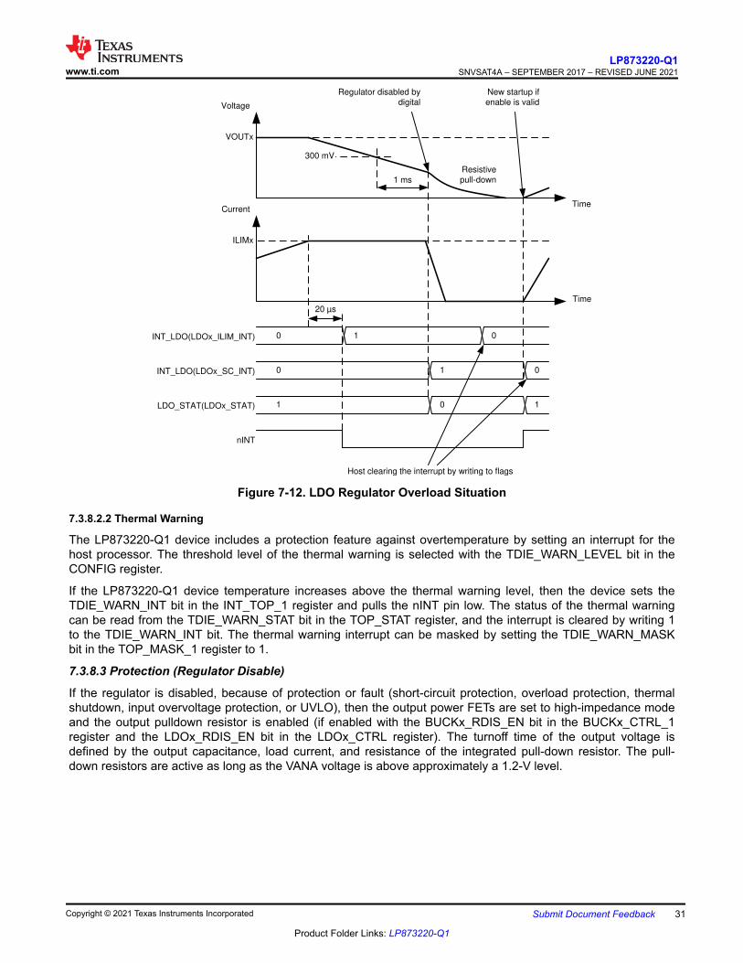
The LDO regulators also include current limit circuitry. If the load current is increased so that the current limit is triggered, the regulator limits the output current to the threshold level. The voltage may decrease if the load current is higher than the current limit. If the current regulation continues for 20 µs, the LP873220-Q1 device sets the LDOx_ILIM_INT bit in the INT_LDO register and pulls the nINT pin low. The host processor can read the LDOx_ILIM_STAT bits in the LDO_STAT register to see if the regulator is still in current regulation mode and the interrupt is cleared by writing 1 to the LDOx_ILIM_INT bit. The current limit interrupt can be masked by setting the LDOx_ILIM_MASK bit in the LDO_MASK register to 1. The LDO overload situation is shown in Figure 7-12.
LP873220-Q1SNVSAT4A – SEPTEMBER 2017 – REVISED JUNE 2021 www.ti.com
30 Submit Document Feedback Copyright © 2021 Texas Instruments Incorporated
Product Folder Links: LP873220-Q1
Time
Voltage
VOUTx
300 mV
Time
Current
ILIMx
INT_LDO(LDOx_ILIM_INT)
20 µs
nINT
LDO_STAT(LDOx_STAT) 1
Resistive pull-down
1
Regulator disabled by digital
Host clearing the interrupt by writing to flags
New startup if enable is valid
1 ms
010
0
INT_LDO(LDOx_SC_INT) 010
Figure 7-12. LDO Regulator Overload Situation
7.3.8.2.2 Thermal Warning
The LP873220-Q1 device includes a protection feature against overtemperature by setting an interrupt for the host processor. The threshold level of the thermal warning is selected with the TDIE_WARN_LEVEL bit in the CONFIG register.
If the LP873220-Q1 device temperature increases above the thermal warning level, then the device sets the TDIE_WARN_INT bit in the INT_TOP_1 register and pulls the nINT pin low. The status of the thermal warning can be read from the TDIE_WARN_STAT bit in the TOP_STAT register, and the interrupt is cleared by writing 1 to the TDIE_WARN_INT bit. The thermal warning interrupt can be masked by setting the TDIE_WARN_MASK bit in the TOP_MASK_1 register to 1.
7.3.8.3 Protection (Regulator Disable)
If the regulator is disabled, because of protection or fault (short-circuit protection, overload protection, thermal shutdown, input overvoltage protection, or UVLO), then the output power FETs are set to high-impedance mode and the output pulldown resistor is enabled (if enabled with the BUCKx_RDIS_EN bit in the BUCKx_CTRL_1 register and the LDOx_RDIS_EN bit in the LDOx_CTRL register). The turnoff time of the output voltage is defined by the output capacitance, load current, and resistance of the integrated pull-down resistor. The pull-down resistors are active as long as the VANA voltage is above approximately a 1.2-V level.
www.ti.comLP873220-Q1
SNVSAT4A – SEPTEMBER 2017 – REVISED JUNE 2021
Copyright © 2021 Texas Instruments Incorporated Submit Document Feedback 31
Product Folder Links: LP873220-Q1

7.3.8.3.1 Short-Circuit and Overload Protection
A short-circuit protection feature allows the LP873220-Q1 to protect itself and the external components against a short circuit at the output or against overload during start-up. For the buck and LDO regulators, the fault thresholds are about 350 mV (buck) and 300 mV (LDO). The protection is triggered and the regulator is disabled if the output voltage is below the threshold level (1 ms) after the regulator is enabled.
In a similar way, the overload situation is protected during normal operation. If the output voltage falls below 0.35 V and 0.3 V and remains below the threshold level for 1 ms, then the regulator is disabled.
In Buck regulator short-circuit and overload situations, the BUCKx_SC_INT bit in the INT_BUCK register and the INT_BUCKx bit in the INT_TOP_1 register are set to 1, the BUCKx_STAT bit in BUCK_STAT register is set to 0, and the nINT signal is pulled low. In LDO regulator short-circuit and overload situations, the LDOx_SC_INT bit in the INT_LDO register and the INT_LDOx bit in the INT_TOP_1 register are set to 1, the LDOx_STAT bit in the LDO_STAT register is set to 0, and the nINT signal is pulled low. The host processor clears the interrupt by writing 1 to the BUCKx_SC_INT or to the LDOx_SC_INT bit. Upon clearing the interrupt, the regulator makes a new start-up attempt if the regulator is in an enabled state.
7.3.8.3.2 Overvoltage Protection
The LP873220-Q1 device monitors the input voltage from the VANA pin in standby and active operation modes. If the input voltage rises above the VANAOVP voltage level, the following occurs:• All regulators are disabled immediately (without switching ramp or shutdown delays).• The pull-down resistors discharge the output voltages, if the pull-down resistors are enabled (the
BUCKx_RDIS_EN = 1 in the BUCKx_CTRL_1 register and the LDOx_RDIS_EN = 1 in the LDOx_CTRL register).
• The GPOs are set to logic low level.• The nINT signal is pulled low.• The OVP_INT bit in the INT_TOP_1 register is set to 1.• The BUCKx_STAT bit in the BUCK_STAT register and the LDOx_STAT bit in the LDO_STAT register are set
to 0.
The host processor clears the interrupt by writing 1 to the OVP_INT bit. If the input voltage is above the overvoltage detection level, then the interrupt is not cleared. The host can read the status of the overvoltage from the OVP_STAT bit in the TOP_STAT register. The regulators cannot be enabled as long as the input voltage is above the overvoltage detection level or while the overvoltage interrupt is pending.
7.3.8.3.3 Thermal Shutdown
The LP873220-Q1 has an overtemperature protection function that operates to protect itself from short-term misuse and overload conditions. When the junction temperature exceeds around 150°C, the regulators are disabled immediately (without switching ramp and shutdown delays), the TDIE_SD_INT bit in the INT_TOP_1 register is set to 1, the nINT signal is pulled low, and the device enters STANDBY. The nINT is cleared by writing 1 to the TDIE_SD_INT bit. If the temperature is above thermal shutdown level, then the interrupt is not cleared. The host can read the status of the thermal shutdown from the TDIE_SD_STAT bit in the TOP_STAT register. The regulators cannot be enabled as long as the junction temperature is above the thermal shutdown level or while the thermal shutdown interrupt is pending.
LP873220-Q1SNVSAT4A – SEPTEMBER 2017 – REVISED JUNE 2021 www.ti.com
32 Submit Document Feedback Copyright © 2021 Texas Instruments Incorporated
Product Folder Links: LP873220-Q1

7.3.8.4 Fault (Power Down)7.3.8.4.1 Undervoltage Lockout
When the input voltage falls below the VANAUVLO at the VANA pin, the buck and LDO regulators are disabled immediately (without switching ramp and shutdown delays), the output capacitor is discharged using the pulldown resistor, and the LP873220-Q1 device enters SHUTDOWN. When the V(VANA) voltage is above the VANAUVLO threshold level, the device powers up to STANDBY state.
If the reset interrupt is unmasked by default (OTP bit for RESET_REG_MASK is 0 in TOP_MASK_2 register), then the RESET_REG_INT interrupt bit in the INT_TOP_2 register indicates that the device has been in SHUTDOWN. The host processor must clear the interrupt by writing 1 to the RESET_REG_INT bit. If the host processor reads the RESET_REG_INT interrupt bit after detecting an nINT low signal, then it detects that the input supply voltage has been below the VANAUVLO level (or the host has requested reset with the SW_RESET bit in the RESET register), and the registers are reset to default values.
7.3.9 Operation of the GPO Signals
The LP873220-Q1 device supports up to two general purpose output signals, GPO and GPO2. The GPO2 signal is multiplexed with the CLKIN signal. The selection between the CLKIN and GPO2 pin function is set with the CLKIN_PIN_SEL bit in the CONFIG register.
The GPO pins are configured with the following bits:• The GPOx_OD bit in The GPO_CTRL register defines the type of the output, either push-pull with V(VANA)
level or open drain.
The logic level of the GPOx pin is set by the EN_GPOx bit in the GPO_CTRL register.
The control of the GPOs can be included to start-up and shutdown sequences. The GPO control for a sequence with an EN pin is selected by the GPOx_EN_PIN_CTRL bit in the GPO_CTRL register. For start-up and shutdown sequence control, see Section 7.3.6.
7.3.10 Digital Signal Filtering
The digital signals have a debounce filtering. The signal or supply is sampled with a clock signal and a counter. This results as an accuracy of one clock period for the debounce window.
Table 7-5. Digital Signal Filtering
EVENT SIGNAL/SUPPLYRISING EDGE FALLING EDGELENGTH LENGTH
Enable/disable for BUCKx, LDOx or GPOx EN 3 µs(1) 3 µs(1)
VANA UVLO VANA 3 µs(1) (VANA voltage rising) Immediate (VANA voltage falling)
VANA overvoltage VANA 1 µs (VANA voltage rising) 20 µs (VANA voltage falling)
Thermal warning TDIE_WARN_INT 20 µs 20 µs
Thermal shutdown TDIE_SD_INT 20 µs 20 µs
Current limit VOUTx_ILIM 20 µs 20 µs
Overload FB_B0, FB_B1, VOUT_LDO0, VOUT_LDO1 1 ms N/V
PGOOD pin and power-good interrupt
PGOOD / FB_B0, FB_B1, VOUT_LDO0, VOUT_LDO1 6 µs 6 µs
(1) No glitch filtering, only synchronization.
www.ti.comLP873220-Q1
SNVSAT4A – SEPTEMBER 2017 – REVISED JUNE 2021
Copyright © 2021 Texas Instruments Incorporated Submit Document Feedback 33
Product Folder Links: LP873220-Q1
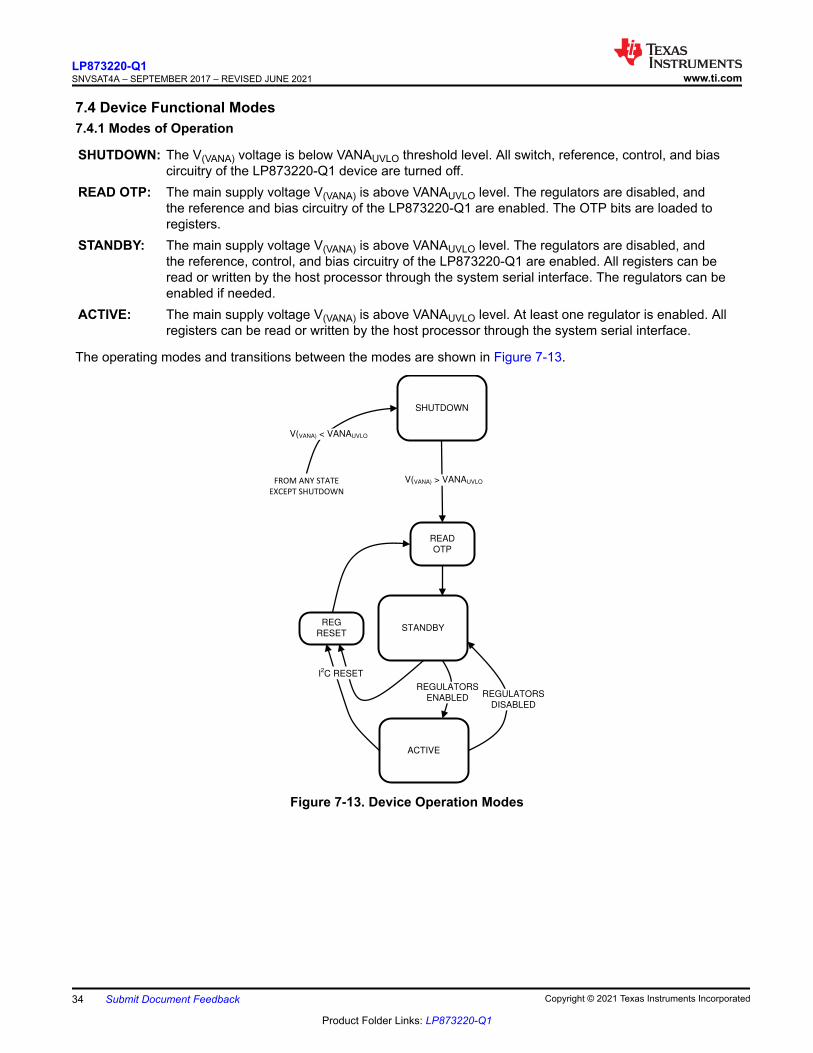
7.4 Device Functional Modes7.4.1 Modes of Operation
SHUTDOWN: The V(VANA) voltage is below VANAUVLO threshold level. All switch, reference, control, and bias circuitry of the LP873220-Q1 device are turned off.
READ OTP: The main supply voltage V(VANA) is above VANAUVLO level. The regulators are disabled, and the reference and bias circuitry of the LP873220-Q1 are enabled. The OTP bits are loaded to registers.
STANDBY: The main supply voltage V(VANA) is above VANAUVLO level. The regulators are disabled, and the reference, control, and bias circuitry of the LP873220-Q1 are enabled. All registers can be read or written by the host processor through the system serial interface. The regulators can be enabled if needed.
ACTIVE: The main supply voltage V(VANA) is above VANAUVLO level. At least one regulator is enabled. All registers can be read or written by the host processor through the system serial interface.
The operating modes and transitions between the modes are shown in Figure 7-13.
SHUTDOWN
STANDBY
ACTIVE
REGULATORS
ENABLED
READ
OTP
REG
RESET
I2C RESET
FROM ANY STATE
EXCEPT SHUTDOWN
REGULATORS
DISABLED
V(VANA) < VANAUVLO
V(VANA) > VANAUVLO
Figure 7-13. Device Operation Modes
LP873220-Q1SNVSAT4A – SEPTEMBER 2017 – REVISED JUNE 2021 www.ti.com
34 Submit Document Feedback Copyright © 2021 Texas Instruments Incorporated
Product Folder Links: LP873220-Q1

7.5 Programming7.5.1 I2C-Compatible Interface
The I2C-compatible synchronous serial interface provides access to the programmable functions and registers on the device. This protocol uses a two-wire interface for bidirectional communications between the ICs connected to the bus. The two interface lines are the serial data line (SDA), and the serial clock line (SCL). Every device on the bus is assigned a unique address, and acts as either a master or a slave depending on whether it generates or receives the serial clock SCL. The SCL and SDA lines must each have a pullup resistor placed on the line and remain HIGH even when the bus is idle. The LP873220-Q1 supports standard mode (100 kHz), fast mode (400 kHz), fast mode plus (1 MHz), and high-speed mode (3.4 MHz).
7.5.1.1 Data Validity
The data on the SDA line must be stable during the HIGH period of the clock signal (SCL). In other words, the state of the data line can only be changed when clock signal is LOW.
data
change
allowed
data
valid
data
change
allowed
data valid
data
change
allowed
SCL
SDA
Figure 7-14. Data Validity Diagram
7.5.1.2 Start and Stop Conditions
The LP873220-Q1 is controlled through an I2C-compatible interface. START and STOP conditions classify the beginning and end of the I2C session. A START condition is defined as SDA transitions from HIGH to LOW while SCL is HIGH. A STOP condition is defined as an SDA transition from LOW to HIGH while SCL is HIGH. The I2C master always generates the START and STOP conditions.
S
SDA
START
Condition
SCL
P
STOP
Condition
Figure 7-15. Start and Stop Sequences
The I2C bus is considered busy after a START condition and free after a STOP condition. During data transmission, the I2C master can generate repeated START conditions. A START and a repeated START condition are equivalent function-wise. The data on SDA must be stable during the HIGH period of the clock signal (SCL). In other words, the state of SDA can only be changed when SCL is LOW. Figure 7-16 shows the SDA and SCL signal timing for the I2C-compatible bus. See Section 6.6 for the timing values.
www.ti.comLP873220-Q1
SNVSAT4A – SEPTEMBER 2017 – REVISED JUNE 2021
Copyright © 2021 Texas Instruments Incorporated Submit Document Feedback 35
Product Folder Links: LP873220-Q1

SCL
SDA
tLOW
trCL
tHD;DAT
tHIGH
tfCL
tSU;DAT
tSU;STA tSU;STO
START REPEATED
START
STOP
tHD;STA
START
tSP
trDA
tBUF
tfDA
tHD;STA
SRS P S
Figure 7-16. I2C-Compatible Timing
7.5.1.3 Transferring Data
Every byte put on the SDA line must be eight bits long, with the most significant bit (MSB) transferred first. Each byte of data has to be followed by an acknowledge bit. The acknowledge-related clock pulse is generated by the master. The master releases the SDA line (HIGH) during the acknowledge clock pulse. The LP873220-Q1 pulls down the SDA line during the 9th clock pulse, signifying an acknowledge. The LP873220-Q1 generates an acknowledge after each byte has been received.
There is one exception to the acknowledge after every byte rule. When the master is the receiver, it must indicate to the transmitter an end of data by not-acknowledging (negative acknowledge) the last byte clocked out of the slave. This negative acknowledge still includes the acknowledge clock pulse (generated by the master), but the SDA line is not pulled down.
Note
If the V(VANA) voltage is below the VANAUVLO threshold level during I2C communication, the LP873220-Q1 device does not drive SDA line. The ACK signal and data transfer to the master is disabled at that time.
After the START condition, the bus master sends a chip address. This address is seven bits long, followed by an eighth bit, which is a data direction bit (READ or WRITE). For the eighth bit, a 0 indicates a WRITE, and a 1 indicates a READ. The second byte selects the register to which the data will be written. The third byte contains data to write to the selected register.
START MSB Chip Address LSB
ACK from slave ACK from slave ACK from slave
SCL
SDA
START id = 0x60 W ACK address = 0x40 ACK ACKaddress 0x40 data STOP
W ACK MSB Register Address LSB ACK MSB Data LSB ACK STOP
Figure 7-17. Write Cycle (w = write; SDA = 0). Example Device Address = 0x60
LP873220-Q1SNVSAT4A – SEPTEMBER 2017 – REVISED JUNE 2021 www.ti.com
36 Submit Document Feedback Copyright © 2021 Texas Instruments Incorporated
Product Folder Links: LP873220-Q1

ACK from slave
START MSB Chip Address LSB
SCL
ACK from slave
W MSB Register Address LSB RS R MSB Data LSB STOP
ACK from slave NACK from masterREPEATED START Data from slave
SDA
START id = 0x60 W ACK address = 0x3F ACK RS R ACK address 0x3F data NACK STOP
MSB Chip Address LSB
id = 0x60
When READ function is to be accomplished, a WRITE function must precede the READ function as shown above.
Figure 7-18. Read Cycle (r = read; SDA = 1). Example Device Address = 0x60
7.5.1.4 I2C-Compatible Chip Address
Note
The device address for the LP873220-Q1 is 0x61.
After the START condition, the I2C master sends the 7-bit address followed by an eighth bit, read or write (R/W). R/W = 0 indicates a WRITE and R/W = 1 indicates a READ. The second byte following the device address selects the register address to which the data is written. The third byte contains the data for the selected register.
1
Bit 7
MSB LSB
I2C Slave Address (chip address)
1
Bit 6
0
Bit 5
0
Bit 4
0
Bit 3
0
Bit 2
0
Bit 1
R/W
Bit 0
Here in an example with device address of 1100000Bin = 60Hex.
Figure 7-19. Device Address Example
7.5.1.5 Auto-Increment Feature
The auto-increment feature allows writing several consecutive registers within one transmission. Every time an 8-bit word is sent to the LP873220-Q1, the internal address index counter is incremented by one and the next register is written. Table 7-6 shows writing sequence to two consecutive registers. The auto-increment feature does not work for read.
Table 7-6. Auto-Increment ExampleMASTER ACTION START
DEVICE ADDRESS = 0x61
WRITE REGISTER ADDRESS DATA DATA STOP
LP873220-Q1 ACK ACK ACK ACK
www.ti.comLP873220-Q1
SNVSAT4A – SEPTEMBER 2017 – REVISED JUNE 2021
Copyright © 2021 Texas Instruments Incorporated Submit Document Feedback 37
Product Folder Links: LP873220-Q1

7.6 Register Maps7.6.1 Register Descriptions
The LP873220-Q1 is controlled by a set of registers through the I2C-compatible interface. The device registers addresses and abbreviations are listed in Table 7-7. A more detailed description is given in the Section 7.6.1.1 to Section 7.6.1.39 sections.
The asterisk (*) marking indicates register bits which are updated from OTP memory during READ OTP state.
Note
This register map describes the default values for a device with orderable code of LP873220RHDRQ1. For other device versions the default values read from OTP memory can be different.
Table 7-7. Summary of LP873220-Q1 Control RegistersAddr Register Read / Write D7 D6 D5 D4 D3 D2 D1 D0
0x00 DEV_REV R DEVICE_ID[1:0] Reserved - do not use
0x01 OTP_REV R OTP_ID[7:0]
0x02 BUCK0_CTRL_1
R/W Reserved - do not use BUCK0_FPWM
BUCK0_RDIS_EN
BUCK0_EN_PIN_CT
RL
BUCK0_EN
0x03 BUCK0_CTRL_2
R/W Reserved - do not use BUCK0_ILIM[2:0] BUCK0_SLEW_RATE[2:0]
0x04 BUCK1_CTRL_1
R/W Reserved - do not use BUCK1_FPWM
BUCK1_RDIS_EN
BUCK1_EN_PIN_CT
RL
BUCK1_EN
0x05 BUCK1_CTRL_2
R/W Reserved - do not use BUCK1_ILIM[2:0] BUCK1_SLEW_RATE[2:0]
0x06 BUCK0_VOUT
R/W BUCK0_VSET[7:0]
0x07 BUCK1_VOUT
R/W BUCK1_VSET[7:0]
0x08 LDO0_CTRL
R/W Reserved - do not use LDO0_RDIS_EN
LDO0_EN_PIN_CT
RL
LDO0_EN
0x09 LDO1_CTRL
R/W Reserved - do not use LDO1_RDIS_EN
LDO1_EN_PIN_CT
RL
LDO1_EN
0x0A LDO0_VOUT
R/W Reserved - do not use LDO0_VSET[4:0]
0x0B LDO1_VOUT
R/W Reserved - do not use LDO1_VSET[4:0]
0x0C BUCK0_DELAY
R/W BUCK0_SHUTDOWN_DELAY[3:0] BUCK0_STARTUP_DELAY[3:0]
0x0D BUCK1_DELAY
R/W BUCK1_SHUTDOWN_DELAY[3:0] BUCK1_STARTUP_DELAY[3:0]
0x0E LDO0_DELAY
R/W LDO0_SHUTDOWN_DELAY[3:0] LDO0_STARTUP_DELAY[3:0]
0x0F LDO1_DELAY
R/W LDO1_SHUTDOWN_DELAY[3:0] LDO1_STARTUP_DELAY[3:0]
0x10 GPO_DELAY
R/W GPO_SHUTDOWN_DELAY[3:0] GPO_STARTUP_DELAY[3:0]
0x11 GPO2_DELAY
R/W GPO2_SHUTDOWN_DELAY[3:0] GPO2_STARTUP_DELAY[3:0]
0x12 GPO_CTRL
R/W Reserved - do not use
GPO2_OD GPO2_EN_PIN_CT
RL
GPO2_EN Reserved - do not use
GPO_OD GPO_EN_PIN_CT
RL
GPO_EN
0x13 CONFIG R/W Reserved - do not use
STARTUP_DELAY_SEL
SHUTDOWN_DELAY_S
EL
CLKIN_PIN_SEL
CLKIN_PD EN_PD TDIE_WARN_LEVEL
EN_SPREAD_SPEC
LP873220-Q1SNVSAT4A – SEPTEMBER 2017 – REVISED JUNE 2021 www.ti.com
38 Submit Document Feedback Copyright © 2021 Texas Instruments Incorporated
Product Folder Links: LP873220-Q1

Table 7-7. Summary of LP873220-Q1 Control Registers (continued)Addr Register Read / Write D7 D6 D5 D4 D3 D2 D1 D0
0x14 PLL_CTRL R/W Reserved - do not use
EN_PLL Reserved - do not use
EXT_CLK_FREQ[4:0]
0x15 PGOOD_CTRL_1
R/W PGOOD_POL
PGOOD_OD PGOOD_WINDOW_LDO
PGOOD_WINDOW_BUC
K
EN_PGOOD_LDO1
EN_PGOOD_LDO0
EN_PGOOD_BUCK1
EN_PGOOD_BUCK0
0x16 PGOOD_CTRL_2
R/W Reserved - do not use EN_PGOOD_TWARN
PG_FAULT_GATES_PG
OOD
PGOOD_MODE
0x17 PG_FAULT R Reserved - do not use PG_FAULT_LDO1
PG_FAULT_LDO0
PG_FAULT_BUCK1
PG_FAULT_BUCK0
0x18 RESET R/W Reserved - do not use SW_RESET
0x19 INT_TOP_1 R/W PGOOD_INT
INT_LDO
INT_BUCK
SYNC_CLK_INT
TDIE_SD_INT
TDIE_WARN_INT
OVP_INT I_MEAS_INT
0x1A INT_TOP_2 R/W Reserved - do not use RESET_REG_INT
0x1B INT_BUCK R/W Reserved - do not use
BUCK1_PG_INT
BUCK1_SC_INT
BUCK1_ILIM_INT
Reserved - do not use
BUCK0_PG_INT
BUCK0_SC_INT
BUCK0_ILIM_INT
0x1C INT_LDO R/W Reserved - do not use
LDO1_PG_INT
LDO1_SC_INT
LDO1_ILIM_INT
Reserved - do not use
LDO0_PG_INT
LDO0_SC_INT
LDO0_ILIM_INT
0x1D TOP_STAT
R PGOOD_STAT
Reserved - do not use SYNC_CLK_STAT
TDIE_SD_STAT
TDIE_WARN_
STAT
OVP_STAT
Reserved - do not use
0x1E BUCK_STAT R BUCK1_STAT
BUCK1_PG_STAT
Reserved - do not use
BUCK1_ILIM_STAT
BUCK0_STAT
BUCK0_PG_STAT
Reserved - do not use
BUCK0_ILIM_STAT
0x1F LDO_STAT R LDO1_STAT
LDO1_PG_STAT
Reserved - do not use
LDO1_ILIM_STAT
LDO0_STAT
LDO0_PG_STAT
Reserved - do not use
LDO0_ILIM_STAT
0x20 TOP_MASK_1
R/W PGOOD_INT_MASK
Reserved - do not use SYNC_CLK_MASK
Reserved - do not use
TDIE_WARN_MASK
Reserved - do not use
I_MEAS_MASK
0x21 TOP_MASK_2
R/W Reserved - do not use RESET_REG_MASK
0x22 BUCK_MASK
R/W BUCK1_PGF_MASK
BUCK1_PGR_MASK
Reserved - do not use
BUCK1_ILIM_MASK
BUCK0_PGF_MASK
BUCK0_PGR_MASK
Reserved - do not use
BUCK0_ILIM_MASK
0x23 LDO_MASK R/W LDO1_PGF_MASK
LDO1_PGR_MASK
Reserved - do not use
LDO1_ILIM_MASK
LDO0_PGF_MASK
LDO0_PGR_MASK
Reserved - do not use
LDO0_ILIM_MASK
0x24 SEL_I_LOAD
R/W Reserved - do not use LOAD_CURRENT_
BUCK_SELECT
0x25 I_LOAD_2 R Reserved - do not use BUCK_LOAD_CURREN
T[8]
0x26 I_LOAD_1 R BUCK_LOAD_CURRENT[7:0]
www.ti.comLP873220-Q1
SNVSAT4A – SEPTEMBER 2017 – REVISED JUNE 2021
Copyright © 2021 Texas Instruments Incorporated Submit Document Feedback 39
Product Folder Links: LP873220-Q1
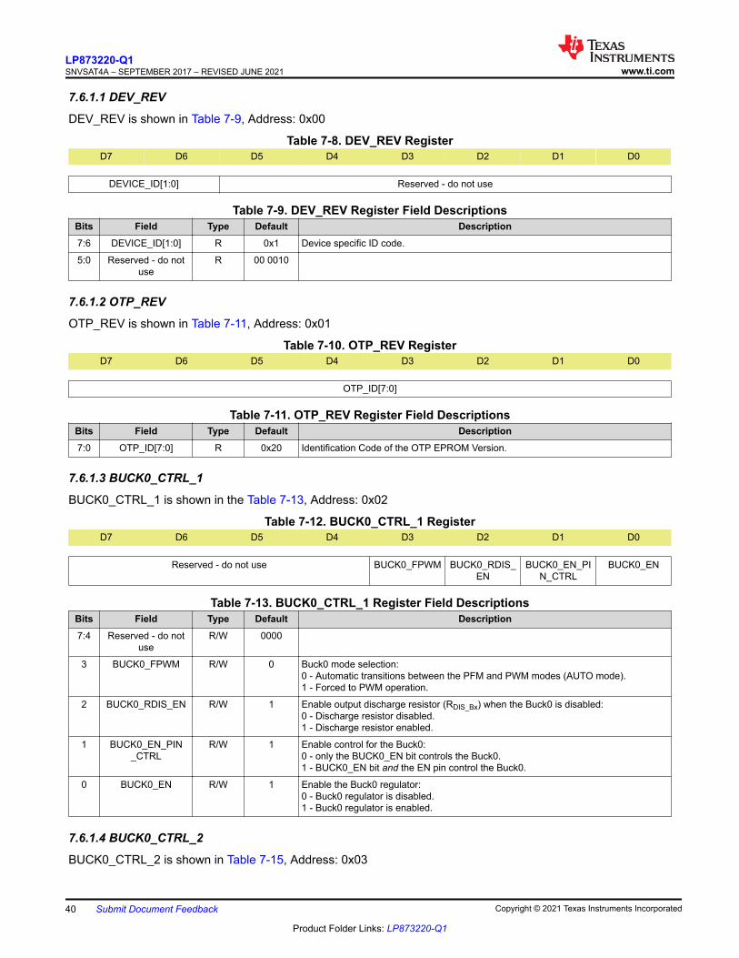
7.6.1.1 DEV_REV
DEV_REV is shown in Table 7-9, Address: 0x00
Table 7-8. DEV_REV RegisterD7 D6 D5 D4 D3 D2 D1 D0
DEVICE_ID[1:0] Reserved - do not use
Table 7-9. DEV_REV Register Field DescriptionsBits Field Type Default Description7:6 DEVICE_ID[1:0] R 0x1 Device specific ID code.
5:0 Reserved - do not use
R 00 0010
7.6.1.2 OTP_REV
OTP_REV is shown in Table 7-11, Address: 0x01
Table 7-10. OTP_REV RegisterD7 D6 D5 D4 D3 D2 D1 D0
OTP_ID[7:0]
Table 7-11. OTP_REV Register Field DescriptionsBits Field Type Default Description7:0 OTP_ID[7:0] R 0x20 Identification Code of the OTP EPROM Version.
7.6.1.3 BUCK0_CTRL_1
BUCK0_CTRL_1 is shown in the Table 7-13, Address: 0x02
Table 7-12. BUCK0_CTRL_1 RegisterD7 D6 D5 D4 D3 D2 D1 D0
Reserved - do not use BUCK0_FPWM BUCK0_RDIS_EN
BUCK0_EN_PIN_CTRL
BUCK0_EN
Table 7-13. BUCK0_CTRL_1 Register Field DescriptionsBits Field Type Default Description7:4 Reserved - do not
useR/W 0000
3 BUCK0_FPWM R/W 0 Buck0 mode selection:0 - Automatic transitions between the PFM and PWM modes (AUTO mode).1 - Forced to PWM operation.
2 BUCK0_RDIS_EN R/W 1 Enable output discharge resistor (RDIS_Bx) when the Buck0 is disabled:0 - Discharge resistor disabled.1 - Discharge resistor enabled.
1 BUCK0_EN_PIN_CTRL
R/W 1 Enable control for the Buck0:0 - only the BUCK0_EN bit controls the Buck0.1 - BUCK0_EN bit and the EN pin control the Buck0.
0 BUCK0_EN R/W 1 Enable the Buck0 regulator:0 - Buck0 regulator is disabled.1 - Buck0 regulator is enabled.
7.6.1.4 BUCK0_CTRL_2
BUCK0_CTRL_2 is shown in Table 7-15, Address: 0x03
LP873220-Q1SNVSAT4A – SEPTEMBER 2017 – REVISED JUNE 2021 www.ti.com
40 Submit Document Feedback Copyright © 2021 Texas Instruments Incorporated
Product Folder Links: LP873220-Q1

Table 7-14. BUCK0_CTRL_2 RegisterD7 D6 D5 D4 D3 D2 D1 D0
Reserved - do not use BUCK0_ILIM[2:0] BUCK0_SLEW_RATE[2:0]
Table 7-15. BUCK0_CTRL_2 Register Field DescriptionsBits Field Type Default Description7:6 Reserved - do not
useR/W 00
5:3 BUCK0_ILIM[2:0] R/W 0x3 Sets the switch current limit of Buck0. Can be programmed at any time during operation:0x0 - 1.5 A0x1 - 2.0 A0x2 - 2.5 A0x3 - 3.0 A0x4 - Reserved - do not use.0x5 - Reserved0x6 - Reserved - do not use.0x7 - Reserved - do not use.
2:0 BUCK0_SLEW_RATE[2:0]
R/W 0x2 Sets the output voltage slew rate for Buck0 regulator (rising and falling edges):0x0 - Reserved - do not use.0x1 - Reserved - do not use.0x2 - 10 mV/µs0x3 - 7.5 mV/µs0x4 - 3.8 mV/µs0x5 - 1.9 mV/µs0x6 - 0.94 mV/µs0x7 - 0.47 mV/µs
7.6.1.5 BUCK1_CTRL_1
BUCK1_CTRL_1 is shown in Table 7-17, Address: 0x04
Table 7-16. BUCK1_CTRL_1 RegisterD7 D6 D5 D4 D3 D2 D1 D0
Reserved - do not use BUCK1_FPWM BUCK1_RDIS_EN
BUCK1_EN_PIN_CTRL
BUCK1_EN
Table 7-17. BUCK1_CTRL_1 Register Field DescriptionsBits Field Type Default Description7:4 Reserved - do not
useR/W 0000
3 BUCK1_FPWM R/W 0 Buck1 mode selection:0 - Automatic transitions between the PFM and PWM modes (AUTO mode).1 - Forced to PWM operation.
2 BUCK1_RDIS_EN R/W 1 Enable output discharge resistor (RDIS_Bx) when the Buck1 is disabled:0 - Discharge resistor is disabled.1 - Discharge resistor is enabled.
1 BUCK1_EN_PIN_CTRL
R/W 1 Enable control for the Buck1:0 - only the BUCK1_EN bit controls the Buck11 - BUCK1_EN bit and the EN pin control the Buck1.
0 BUCK1_EN R/W 1 Enable the Buck1 regulator:0 - Buck1 regulator is disabled.1 - Buck1 regulator is enabled.
7.6.1.6 BUCK1_CTRL_2
BUCK1_CTRL_2 is shown in Table 7-19, Address: 0x05
www.ti.comLP873220-Q1
SNVSAT4A – SEPTEMBER 2017 – REVISED JUNE 2021
Copyright © 2021 Texas Instruments Incorporated Submit Document Feedback 41
Product Folder Links: LP873220-Q1
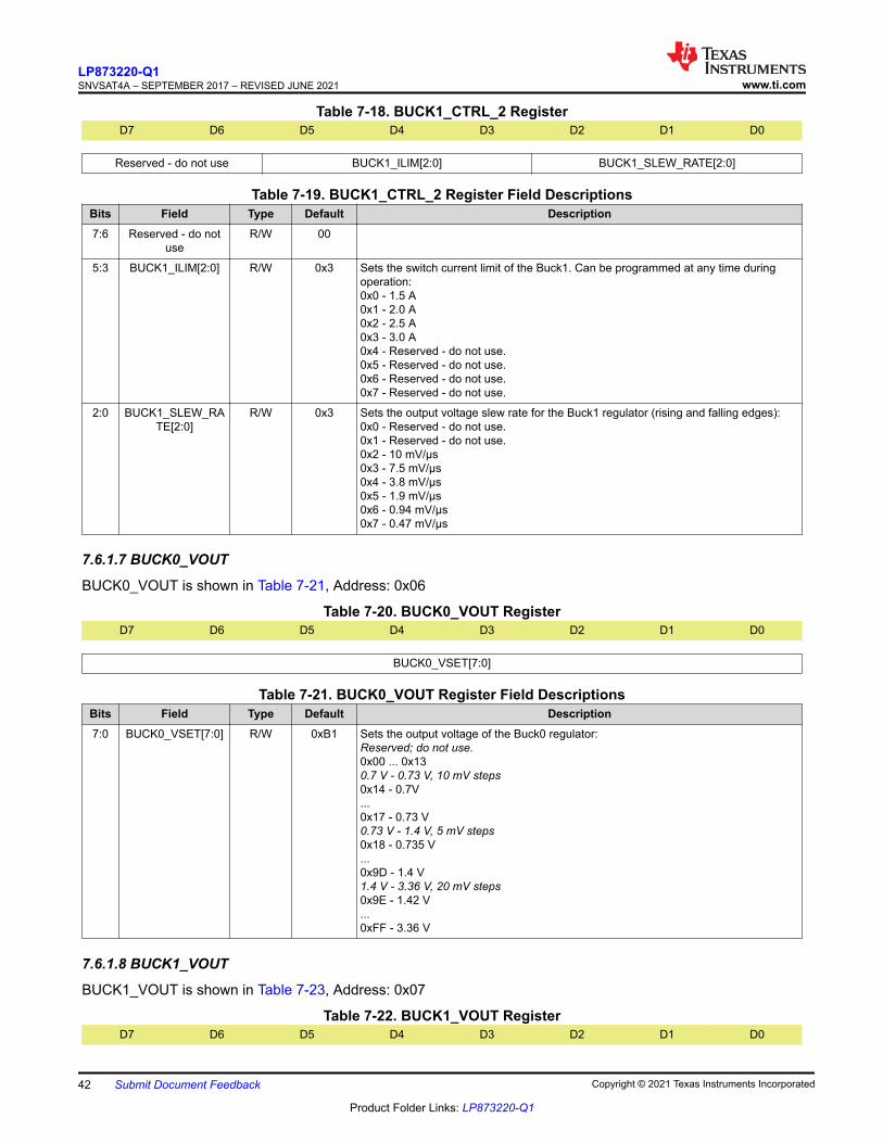
Table 7-18. BUCK1_CTRL_2 RegisterD7 D6 D5 D4 D3 D2 D1 D0
Reserved - do not use BUCK1_ILIM[2:0] BUCK1_SLEW_RATE[2:0]
Table 7-19. BUCK1_CTRL_2 Register Field DescriptionsBits Field Type Default Description7:6 Reserved - do not
useR/W 00
5:3 BUCK1_ILIM[2:0] R/W 0x3 Sets the switch current limit of the Buck1. Can be programmed at any time during operation:0x0 - 1.5 A0x1 - 2.0 A0x2 - 2.5 A0x3 - 3.0 A0x4 - Reserved - do not use.0x5 - Reserved - do not use.0x6 - Reserved - do not use.0x7 - Reserved - do not use.
2:0 BUCK1_SLEW_RATE[2:0]
R/W 0x3 Sets the output voltage slew rate for the Buck1 regulator (rising and falling edges):0x0 - Reserved - do not use.0x1 - Reserved - do not use.0x2 - 10 mV/µs0x3 - 7.5 mV/µs0x4 - 3.8 mV/µs0x5 - 1.9 mV/µs0x6 - 0.94 mV/µs0x7 - 0.47 mV/µs
7.6.1.7 BUCK0_VOUT
BUCK0_VOUT is shown in Table 7-21, Address: 0x06
Table 7-20. BUCK0_VOUT RegisterD7 D6 D5 D4 D3 D2 D1 D0
BUCK0_VSET[7:0]
Table 7-21. BUCK0_VOUT Register Field DescriptionsBits Field Type Default Description7:0 BUCK0_VSET[7:0] R/W 0xB1 Sets the output voltage of the Buck0 regulator:
Reserved; do not use.0x00 ... 0x130.7 V - 0.73 V, 10 mV steps0x14 - 0.7V...0x17 - 0.73 V0.73 V - 1.4 V, 5 mV steps0x18 - 0.735 V...0x9D - 1.4 V1.4 V - 3.36 V, 20 mV steps0x9E - 1.42 V...0xFF - 3.36 V
7.6.1.8 BUCK1_VOUT
BUCK1_VOUT is shown in Table 7-23, Address: 0x07
Table 7-22. BUCK1_VOUT RegisterD7 D6 D5 D4 D3 D2 D1 D0
LP873220-Q1SNVSAT4A – SEPTEMBER 2017 – REVISED JUNE 2021 www.ti.com
42 Submit Document Feedback Copyright © 2021 Texas Instruments Incorporated
Product Folder Links: LP873220-Q1

BUCK1_VSET[7:0]
Table 7-23. BUCK1_VOUT Register Field DescriptionsBits Field Type Default Description7:0 BUCK1_VSET[7:0] R/W 0x93 Sets the output voltage of the Buck0 regulator:
Reserved; do not use.0x00 ... 0x130.7 V - 0.73 V, 10 mV steps0x14 - 0.7V...0x17 - 0.73 V0.73 V - 1.4 V, 5 mV steps0x18 - 0.735 V...0x9D - 1.4 V1.4 V - 3.36 V, 20 mV steps0x9E - 1.42 V...0xFF - 3.36 V
7.6.1.9 LDO0_CTRL
LDO0_CTRL is shown in Table 7-25, Address: 0x08
Table 7-24. LDO0_CTRL RegisterD7 D6 D5 D4 D3 D2 D1 D0
Reserved - do not use LDO0_RDIS_EN
LDO0_EN_PIN_CTRL
LDO0_EN
Table 7-25. LDO0_CTRL Register Field DescriptionsBits Field Type Default Description7:3 Reserved - do not
useR/W 0 0000
2 LDO0_RDIS_EN R/W 1 Enable output discharge resistor (RDIS_LDOx) when the LDO0 is disabled:0 - Discharge resistor is disabled.1 - Discharge resistor is enabled.
1 LDO0_EN_PIN_CTRL
R/W 1 Enable control for the LDO0:0 - only the LDO0_EN bit controls the LDO0.1 - LDO0_EN bit and the EN pin control the LDO0.
0 LDO0_EN R/W 1 Enable the LDO0 regulator:0 - LDO0 regulator is disabled.1 - LDO0 regulator is enabled.
7.6.1.10 LDO1_CTRL
LDO1_CTRL is shown in Table 7-27, Address: 0x09
Table 7-26. LDO1_CTRL RegisterD7 D6 D5 D4 D3 D2 D1 D0
Reserved - do not use LDO1_RDIS_EN
LDO1_EN_PIN_CTRL
LDO1_EN
Table 7-27. LDO1_CTRL Register Field DescriptionsBits Field Type Default Description7:3 Reserved - do not
useR/W 0 0000
2 LDO1_RDIS_EN R/W 1 Enable output discharge resistor (RDIS_LDOx) when the LDO1 is disabled:0 - Discharge resistor is disabled.1 - Discharge resistor is enabled.
www.ti.comLP873220-Q1
SNVSAT4A – SEPTEMBER 2017 – REVISED JUNE 2021
Copyright © 2021 Texas Instruments Incorporated Submit Document Feedback 43
Product Folder Links: LP873220-Q1

Table 7-27. LDO1_CTRL Register Field Descriptions (continued)Bits Field Type Default Description
1 LDO1_EN_PIN_CTRL
R/W 1 Enable control for the LDO1:0 - only the LDO1_EN bit controls the LDO1.1 - LDO1_EN bit and the EN pin control the LDO1.
0 LDO1_EN R/W 1 Enable the LDO1 regulator:0 - LDO1 regulator is disabled.1 - LDO1 regulator is enabled.
7.6.1.11 LDO0_VOUT
LDO0_VOUT is shown in Table 7-29, Address: 0x0A
Table 7-28. LDO0_VOUT RegisterD7 D6 D5 D4 D3 D2 D1 D0
Reserved - do not use LDO0_VSET[4:0]
Table 7-29. LDO0_VOUT Register Field DescriptionsBits Field Type Default Description7:5 Reserved - do not
useR/W 000
4:0 LDO0_VSET[4:0] R/W 0xA Sets the output voltage of the LDO0 regulator:0.8 V - 3.3 V, 100 mV steps0x00 - 0.8V...0x19 - 3.3 VReserved; do not use.0x1A ... 0x1F
7.6.1.12 LDO1_VOUT
LDO1_VOUT is shown in Table 7-31, Address: 0x0B
Table 7-30. LDO1_VOUT RegisterD7 D6 D5 D4 D3 D2 D1 D0
Reserved - do not use LDO1_VSET[4:0]
Table 7-31. LDO1_VOUT Register Field DescriptionsBits Field Type Default Description7:5 Reserved - do not
useR/W 000
4:0 LDO1_VSET[4:0] R/W 0xA Sets the output voltage of the LDO1 regulator:0.8 V - 3.3 V, 100 mV steps0x00 - 0.8V...0x19 - 3.3 VReserved; do not use.0x1A ... 0x1F
7.6.1.13 BUCK0_DELAY
BUCK0_DELAY is shown in Table 7-33, Address: 0x0C
Table 7-32. BUCK0_DELAY RegisterD7 D6 D5 D4 D3 D2 D1 D0
BUCK0_SHUTDOWN_DELAY[3:0] BUCK0_STARTUP_DELAY[3:0]
LP873220-Q1SNVSAT4A – SEPTEMBER 2017 – REVISED JUNE 2021 www.ti.com
44 Submit Document Feedback Copyright © 2021 Texas Instruments Incorporated
Product Folder Links: LP873220-Q1

Table 7-33. BUCK0_DELAY Register Field DescriptionsBits Field Type Default Description7:4 BUCK0_
SHUTDOWN_DELAY[3:0]
R/W 0xA Shutdown delay of the Buck0 from the EN signal's falling edge:0x0 - 0 ms0x1 - 0.5 ms (1 ms if SHUTDOWN_DELAY_SEL=1 in the CONFIG register.)...0xF - 7.5 ms (15 ms if SHUTDOWN_DELAY_SEL=1 in the CONFIG register.)
3:0 BUCK0_STARTUP_DELAY[3:0]
R/W 0x0 Startup delay of the Buck0 from the EN signal's rising edge:0x0 - 0 ms0x1 - 0.5 ms (1 ms if STARTUP_DELAY_SEL=1 in the CONFIG register.)...0xF - 7.5 ms (15 ms if STARTUP_DELAY_SEL=1 in the CONFIG register.)
7.6.1.14 BUCK1_DELAY
BUCK1_DELAY is shown in Table 7-35, Address: 0x0D
Table 7-34. BUCK1_DELAY RegisterD7 D6 D5 D4 D3 D2 D1 D0
BUCK1_SHUTDOWN_DELAY[3:0] BUCK1_STARTUP_DELAY[3:0]
Table 7-35. BUCK1_DELAY Register Field DescriptionsBits Field Type Default Description7:4 BUCK1_
SHUTDOWN_DELAY[3:0]
R/W 0x3 Shutdown delay of the Buck1 from the EN signal's falling edge:0x0 - 0 ms0x1 - 0.5 ms (1 ms if SHUTDOWN_DELAY_SEL=1 in the CONFIG register.)...0xF - 7.5 ms (15 ms if SHUTDOWN_DELAY_SEL=1 in the CONFIG register.)
3:0 BUCK1_STARTUP_DELAY[3:0]
R/W 0x2 Startup delay of the Buck1 from the EN signal's rising edge:0x0 - 0 ms0x1 - 0.5 ms (1 ms if STARTUP_DELAY_SEL=1 in the CONFIG register.)...0xF - 7.5 ms (15 ms if STARTUP_DELAY_SEL=1 in the CONFIG register.)
7.6.1.15 LDO0_DELAY
LDO0_DELAY is shown in Table 7-37, Address: 0x0E
Table 7-36. LDO0_DELAY RegisterD7 D6 D5 D4 D3 D2 D1 D0
LDO0_SHUTDOWN_DELAY[3:0] LDO0_STARTUP_DELAY[3:0]
Table 7-37. LDO0_DELAY Register Field DescriptionsBits Field Type Default Description7:4 LDO0_
SHUTDOWN_DELAY[3:0]
R/W 0x3 Shutdown delay of the LDO0 from the EN signal's falling edge:0x0 - 0 ms0x1 - 0.5 ms (1 ms if SHUTDOWN_DELAY_SEL=1 in the CONFIG register.)...0xF - 7.5 ms (15 ms if SHUTDOWN_DELAY_SEL=1 in the CONFIG register.)
3:0 LDO0_STARTUP_DELAY[3:0]
R/W 0x1 Startup delay of the LDO0 from the EN signal's rising edge:0x0 - 0 ms0x1 - 0.5 ms (1 ms if STARTUP_DELAY_SEL=1 in the CONFIG register.)...0xF - 7.5 ms (15 ms if STARTUP_DELAY_SEL=1 in the CONFIG register.)
7.6.1.16 LDO1_DELAY
LDO1_DELAY is shown in Table 7-39, Address: 0x0F
www.ti.comLP873220-Q1
SNVSAT4A – SEPTEMBER 2017 – REVISED JUNE 2021
Copyright © 2021 Texas Instruments Incorporated Submit Document Feedback 45
Product Folder Links: LP873220-Q1

Table 7-38. LDO1_DELAY RegisterD7 D6 D5 D4 D3 D2 D1 D0
LDO1_SHUTDOWN_DELAY[3:0] LDO1_STARTUP_DELAY[3:0]
Table 7-39. LDO1_DELAY Register Field DescriptionsBits Field Type Default Description7:4 LDO1_
SHUTDOWN_DELAY[3:0]
R/W 0x2 Shutdown delay of the LDO1 from the EN signal's falling edge:0x0 - 0 ms0x1 - 0.5 ms (1 ms if SHUTDOWN_DELAY_SEL=1 in the CONFIG register.)...0xF - 7.5 ms (15 ms if SHUTDOWN_DELAY_SEL=1 in the CONFIG register.)
3:0 LDO1_STARTUP_DELAY[3:0]
R/W 0x6 Startup delay of the LDO1 from the EN signal's rising edge:0x0 - 0 ms0x1 - 0.5 ms (1 ms if STARTUP_DELAY_SEL=1 in the CONFIG register.)...0xF - 7.5 ms (15 ms if STARTUP_DELAY_SEL=1 in the CONFIG register.)
7.6.1.17 GPO_DELAY
GPO_DELAY is shown in Table 7-41, Address: 0x10
Table 7-40. GPO_DELAY RegisterD7 D6 D5 D4 D3 D2 D1 D0
GPO_SHUTDOWN_DELAY[3:0] GPO_STARTUP_DELAY[3:0]
Table 7-41. GPO_DELAY Register Field DescriptionsBits Field Type Default Description7:4 GPO_
SHUTDOWN_DELAY[3:0]
R/W 0x0 Delay for the GPO falling edge from the EN signal's falling edge:0x0 - 0 ms0x1 - 0.5 ms (1 ms if SHUTDOWN_DELAY_SEL=1 in the CONFIG register)...0xF - 7.5 ms (15 ms if SHUTDOWN_DELAY_SEL=1 in the CONFIG register)
3:0 GPO_STARTUP_DELAY[3:0]
R/W 0xA Delay for the GPO rising edge from the EN signal's rising edge:0x0 - 0 ms0x1 - 0.5 ms (1 ms if STARTUP_DELAY_SEL=1 in the CONFIG register.)...0xF - 7.5 ms (15 ms if STARTUP_DELAY_SEL=1 in the CONFIG register.)
7.6.1.18 GPO2_DELAY
GPO2_DELAY is shown in Table 7-43, Address: 0x11
Table 7-42. GPO2_DELAY RegisterD7 D6 D5 D4 D3 D2 D1 D0
GPO2_SHUTDOWN_DELAY[3:0] GPO2_STARTUP_DELAY[3:0]
Table 7-43. GPO2_DELAY Register Field DescriptionsBits Field Type Default Description7:4 GPO2_
SHUTDOWN_DELAY[3:0]
R/W 0x3 Delay for the GPO2 falling edge from the EN signal's falling edge:0x0 - 0 ms0x1 - 0.5 ms (1 ms if SHUTDOWN_DELAY_SEL=1 in the CONFIG register.)...0xF - 7.5 ms (15 ms if SHUTDOWN_DELAY_SEL=1 in the CONFIG register.)
LP873220-Q1SNVSAT4A – SEPTEMBER 2017 – REVISED JUNE 2021 www.ti.com
46 Submit Document Feedback Copyright © 2021 Texas Instruments Incorporated
Product Folder Links: LP873220-Q1

Table 7-43. GPO2_DELAY Register Field Descriptions (continued)Bits Field Type Default Description3:0 GPO2_
STARTUP_DELAY[3:0]
R/W 0x2 Delay for the GPO2 rising edge from the EN signal's rising edge:0x0 - 0 ms0x1 - 0.5 ms (1 ms if STARTUP_DELAY_SEL=1 in the CONFIG register.)...0xF - 7.5 ms (15 ms if STARTUP_DELAY_SEL=1 in the CONFIG register.)
7.6.1.19 GPO_CTRL
GPO_CTRL is shown in Table 7-45, Address: 0x12
Table 7-44. GPO_CTRL RegisterD7 D6 D5 D4 D3 D2 D1 D0
Reserved - do not use
GPO2_OD GPO2_EN_PIN_CTRL
GPO2_EN Reserved - do not use
GPO_OD GPO_EN_PIN_CTRL
GPO_EN
Table 7-45. GPO_CTRL Register Field DescriptionsBits Field Type Default Description
7 Reserved - do not use
R 0
6 GP02_OD R/W 1 GPO2 signal type when configured as the General Purpose Output (CLKIN pin):0 - Push-pull output (VANA level)1 - Open-drain output
5 GPO2_EN_PIN_CTRL
R/W 1 Control for the GPO2:0 - Only the GPO2_EN bit controls the GPO21 - GPO2_EN bit and the EN pin control the GPO2.
4 GPO2_EN R/W 1 Output level of the GPO2 signal (when configured as the General Purpose Output):0 - Logic low level1 - Logic high level
3 Reserved - do not use
R 0
2 GPO_OD R/W 1 GPO signal type:0 - Push-pull output (VANA level)1 - Open-drain output
1 GPO_EN_PIN_CTRL
R/W 1 Control for the GPO:0 - Only the GPO_EN bit controls the GPO1 - GPO_EN bit and the EN pin control the GPO.
0 GPO_EN R/W 1 Output level of the GPO signal:0 - Logic low level1 - Logic high level
7.6.1.20 CONFIG
CONFIG is shown in Table 7-47, Address: 0x13
Table 7-46. CONFIG RegisterD7 D6 D5 D4 D3 D2 D1 D0
Reserved - do not use
STARTUP_DELAY_SEL
SHUTDOWN_DELAY_SEL
CLKIN_PIN_SEL
CLKIN_PD EN2_PD TDIE_WARN_LEVEL
EN_SPREAD_SPEC
Table 7-47. CONFIG Register Field DescriptionsBits Field Type Default Description
7 Reserved - do not use
R/W 0
6 STARTUP_DELAY_SEL
R/W 0 Startup delay range from the EN signals:0 - 0 ms - 7.5 ms with 0.5 ms steps1 - 0 ms - 15 ms with 1 ms steps
www.ti.comLP873220-Q1
SNVSAT4A – SEPTEMBER 2017 – REVISED JUNE 2021
Copyright © 2021 Texas Instruments Incorporated Submit Document Feedback 47
Product Folder Links: LP873220-Q1

Table 7-47. CONFIG Register Field Descriptions (continued)Bits Field Type Default Description
5 SHUTDOWN_DELAY_SEL
R/W 0 Shutdown delay range from the EN signals:0 - 0 ms - 7.5 ms with 0.5 ms steps1 - 0 ms - 15 ms with 1 ms steps
4 CLKIN_PIN_SEL R/W 0 CLKIN pin function:0 - GPO21 - CLKIN
3 CLKIN_PD R/W 0 Selects the pull down resistor on the CLKIN input pin (valid also when selected as GPO2):0 - Pull-down resistor is disabled.1 - Pull-down resistor is enabled.
2 EN_PD R/W 1 Selects the pull down resistor on the EN input pin.0 - Pull-down resistor is disabled.1 - Pull-down resistor is enabled.
1 TDIE_WARN_LEVEL
R/W 1 Thermal warning threshold level:0 - 125°C1 - 137°C
0 EN_SPREAD_SPEC
R/W 0 Enable spread spectrum feature:0 - Disabled1 - Enabled
7.6.1.21 PLL_CTRL
PLL_CTRL is shown in Table 7-49, Address: 0x14
Table 7-48. PLL_CTRL RegisterD7 D6 D5 D4 D3 D2 D1 D0
Reserved - do not use
EN_PLL Reserved - do not use
EXT_CLK_FREQ[4:0]
Table 7-49. PLL_CTRL Register Field DescriptionsBits Field Type Default Description
7 Reserved - do not use
R/W 0
6 EN_PLL R/W 0 Selection of the external clock and PLL operation:0 - Forced to the internal RC oscillator. The PLL is disabled.1 - PLL is enabled in the STANDBY and ACTIVE modes. Automatic external clock use when available, and interrupt is generated if the external clock appears or disappears.
5 Reserved - do not use
R/W 0 This bit must be set to '''0 .''
4:0 EXT_CLK_FREQ[4:0]
R/W 0x1 Frequency of the external clock (CLKIN):0x00 - 1 MHz0x01 - 2 MHz0x02 - 3 MHz...0x16 - 23 MHz0x17 - 24 MHz0x18...0x1F - Reserved - do not useSee electrical specification for the input clock frequency tolerance.
7.6.1.22 PGOOD_CTRL_1
PGOOD_CTRL_1 is shown in Table 7-51, Address: 0x15
Table 7-50. PGOOD_CTRL_1 RegisterD7 D6 D5 D4 D3 D2 D1 D0
LP873220-Q1SNVSAT4A – SEPTEMBER 2017 – REVISED JUNE 2021 www.ti.com
48 Submit Document Feedback Copyright © 2021 Texas Instruments Incorporated
Product Folder Links: LP873220-Q1

PGOOD_POL PGOOD_OD PGOOD_WINDOW_LDO
PGOOD_WINDOW_BUC
K
EN_PGOOD_LDO1
EN_PGOOD_LDO0
EN_PGOOD_BUCK1
EN_PGOOD_BUCK0
Table 7-51. PGOOD_CTRL_1 Register Field DescriptionsBits Field Type Default Description
7 PGOOD_POL R/W 0 PGOOD signal polarity:0 - PGOOD signal high when the monitored outputs are valid.1 - PGOOD signal low when the monitored outputs are valid.
6 PGOOD_OD R/W 1 PGOOD signal type:0 - Push-pull output (VANA level)1 - Open-drain output
5 PGOOD_WINDOW_LDO
R/W 1 LDO Output voltage monitoring method for the PGOOD signal:0 - Only undervoltage monitoring1 - Overvoltage and undervoltage monitoring
4 PGOOD_WINDOW_BUCK
R/W 1 Buck Output voltage monitoring method for the PGOOD signal:0 - Only undervoltage monitoring1 - Overvoltage and undervoltage monitoring
3 EN_PGOOD_LDO1 R/W 1 PGOOD signal source control from LDO1:0 - LDO1 is not monitored.1 - LDO1 Power-Good threshold voltage is monitored.
2 EN_PGOOD_LDO0 R/W 1 PGOOD signal source control from theLDO0:0 - LDO0 is not monitored.1 - LDO0 Power-Good threshold voltage is monitored.
1 EN_PGOOD_BUCK1
R/W 1 PGOOD signal source control from the Buck1:0 - Buck1 is not monitored.1 - Buck1 Power-Good threshold voltage is monitored.
0 EN_PGOOD_BUCK0
R/W 1 PGOOD signal source control from the Buck0:0 - Buck0 is not monitored.1 - Buck0 Power-Good threshold voltage is monitored.
7.6.1.23 PGOOD_CTRL_2
PGOOD_CTRL_2 is shown in Table 7-53, Address: 0x16
Table 7-52. PGOOD_CTRL_2 RegisterD7 D6 D5 D4 D3 D2 D1 D0
Reserved - do not use EN_PGOOD_TWARN
PG_FAULT_GATES_PGOOD
PGOOD_MODE
Table 7-53. PGOOD_CTRL_2 Register Field DescriptionsBits Field Type Default Description7:3 Reserved - do not
useR/W 0 0000
2 EN_PGOOD_TWARN
R/W 1 Thermal warning control for the PGOOD signal:0 - Thermal warning is not monitored.1 - PGOOD inactive if the thermal warning flag is active.
1 PG_FAULT_GATES_PGOOD
R/W 0 Type of operation for the PGOOD signal:0 - Indicates live status of monitored voltage outputs.1 - Indicates status of the PG_FAULT register, inactive when at least one PG_FAULT_x bit is inactive.
0 PGOOD_MODE R/W 0 Operating mode for the PGOOD signal:0 - Gated mode1 - Continuous mode
7.6.1.24 PG_FAULT
PG_FAULT is shown in Table 7-55, Address: 0x17
www.ti.comLP873220-Q1
SNVSAT4A – SEPTEMBER 2017 – REVISED JUNE 2021
Copyright © 2021 Texas Instruments Incorporated Submit Document Feedback 49
Product Folder Links: LP873220-Q1

Table 7-54. PG_FAULT RegisterD7 D6 D5 D4 D3 D2 D1 D0
Reserved - do not use PG_FAULT_LDO1
PG_FAULT_LDO0
PG_FAULT_BUCK1
PG_FAULT_BUCK0
Table 7-55. PG_FAULT Register Field DescriptionsBits Field Type Default Description7:4 Reserved - do not
useR/W 0000
3 PG_FAULT_LDO1 R/W 0 Source for the PGOOD inactive signal:0 - LDO1 has not set the PGOOD signal inactive.1 - LDO1 is selected for the PGOOD signal and it has set the PGOOD signal inactive. This bit can be cleared by writing '1' to this bit when the LDO1 output is valid.
2 PG_FAULT_LDO0 R/W 0 Source for PGOOD inactive signal:0 - LDO0 has not set the PGOOD signal inactive.1 - LDO0 is selected for the PGOOD signal and it has set the PGOOD signal inactive. This bit can be cleared by writing '1' to this bit when the LDO0 output is valid.
1 PG_FAULT_BUCK1 R/W 0 Source for PGOOD inactive signal:0 - Buck1 has not set PGOOD signal inactive.1 - Buck1 is selected for the PGOOD signal and it has set the PGOOD signal inactive. This bit can be cleared by writing '1' to this bit when the Buck1 output is valid.
0 PG_FAULT_BUCK0 R/W 0 Source for PGOOD inactive signal:0 - Buck0 has not set PGOOD signal inactive.1 - Buck0 is selected for the PGOOD signal and it has set the PGOOD signal inactive. This bit can be cleared by writing '1' to this bit when the Buck0 output is valid.
7.6.1.25 RESET
RESET is shown in Table 7-57, Address: 0x18
Table 7-56. RESET RegisterD7 D6 D5 D4 D3 D2 D1 D0
Reserved - do not use SW_RESET
Table 7-57. RESET Register Field DescriptionsBits Field Type Default Description7:1 Reserved - do not
useR/W 000 0000
0 SW_RESET R/W 0 Software commanded reset. When written to 1, the registers will be reset to the default values, the OTP memory is read, and the I2C interface is reset.The bit is automatically cleared.
7.6.1.26 INT_TOP_1
INT_TOP_1 is shown in Table 7-59, Address: 0x19
Table 7-58. INT_TOP_1 RegisterD7 D6 D5 D4 D3 D2 D1 D0
PGOOD_INT LDO_INT BUCK_INT SYNC_CLK_INT
TDIE_SD_INT TDIE_WARN_INT
OVP_INT I_MEAS_INT
Table 7-59. INT_TOP_1 Register Field DescriptionsBits Field Type Default Description
7 PGOOD_INT R/W 0 Latched status bit indicating that the PGOOD pin has changed from active to inactive.Write 1 to clear interrupt.
LP873220-Q1SNVSAT4A – SEPTEMBER 2017 – REVISED JUNE 2021 www.ti.com
50 Submit Document Feedback Copyright © 2021 Texas Instruments Incorporated
Product Folder Links: LP873220-Q1

Table 7-59. INT_TOP_1 Register Field Descriptions (continued)Bits Field Type Default Description
6 LDO_INT R 0 Interrupt indicating that the LDO1 and LDO0 have a pending interrupt. The reason for the interrupt is indicated in the INT_LDO register.This bit is cleared automatically when the INT_LDO register is cleared to 0x00.
5 BUCK_INT R 0 Interrupt indicating that the Buck1 and Buck0 have a pending interrupt. The reason for the interrupt is indicated in the INT_BUCK register.This bit is cleared automatically when INT_BUCK register is cleared to 0x00.
4 SYNC_CLK_INT R/W 0 Latched status bit indicating that the external clock has appeared or disappeared.Write 1 to clear interrupt.
3 TDIE_SD_INT R/W 0 Latched status bit indicating that the die junction temperature has exceeded the thermal shutdown level. The regulators have been disabled if they were enabled and the GPO and GPO2 signals are driven low. The regulators cannot be enabled if this bit is active. The actual status of the thermal shutdown is indicated by the TDIE_SD_STAT bit in the TOP_STAT register.Write 1 to clear interrupt.
2 TDIE_WARN_INT R/W 0 Latched status bit indicating that the die junction temperature has exceeded the thermal warning level. The actual status of the thermal warning is indicated by the TDIE_WARN_STAT bit in the TOP_STAT register.Write 1 to clear interrupt.
1 OVP_INT R/W 0 Latched status bit indicating that the input voltage has exceeded the over-voltage detection level. The regulators have been disabled if they were enabled and the GPO and GPO2 signals are driven low. The actual status of the over-voltage is indicated by the OVP_STAT bit in the TOP_STAT register.Write 1 to clear interrupt.
0 I_MEAS_INT R/W 0 Latched status bit indicating that the load current measurement result is available in the I_LOAD_1 and I_LOAD_2 registers.Write 1 to clear interrupt.
7.6.1.27 INT_TOP_2
INT_TOP_2 is shown in Table 7-61, Address: 0x1A
Table 7-60. INT_TOP_2 RegisterD7 D6 D5 D4 D3 D2 D1 D0
Reserved - do not use RESET_REG_INT
Table 7-61. INT_TOP_2 Register Field DescriptionsBits Field Type Default Description7:1 Reserved - do not
useR/W 000 0000
0 RESET_REG_INT R/W 0 Latched status bit indicating that either VANA supply voltage has been below the undervoltage threshold level or the host has requested a reset using the SW_RESET bit in RESET register. The regulators have been disabled, the registers are reset to the default values, and the normal startup procedure is done.Write 1 to clear interrupt.
7.6.1.28 INT_BUCK
INT_BUCK is shown in Table 7-63, Address: 0x1B
Table 7-62. INT_BUCK RegisterD7 D6 D5 D4 D3 D2 D1 D0
Reserved - do not use
BUCK1_PG_INT
BUCK1_SC_INT
BUCK1_ILIM_INT
Reserved - do not use
BUCK0_PG_INT
BUCK0_SC_INT
BUCK0_ILIM_INT
www.ti.comLP873220-Q1
SNVSAT4A – SEPTEMBER 2017 – REVISED JUNE 2021
Copyright © 2021 Texas Instruments Incorporated Submit Document Feedback 51
Product Folder Links: LP873220-Q1

Table 7-63. INT_BUCK Register Field DescriptionsBits Field Type Default Description
7 Reserved - do not use
R/W 0
6 BUCK1_PG_INT R/W 0 Latched status bit indicating that Buck1 Power-Good event has been detected.Write 1 to clear.
5 BUCK1_SC_INT R/W 0 Latched status bit indicating that the Buck1 output voltage has been over 1 ms below the short-circuit threshold level.Write 1 to clear.
4 BUCK1_ILIM_INT R/W 0 Latched status bit indicating that the Buck1 output current limit has been active.Write 1 to clear.
3 Reserved - do not use
R/W 0
2 BUCK0_PG_INT R/W 0 Latched status bit indicating that the Buck0 Power-Good event has been detected.Write 1 to clear.
1 BUCK0_SC_INT R/W 0 Latched status bit indicating that the Buck0 output voltage has been over 1 ms below the short-circuit threshold level.Write 1 to clear.
0 BUCK0_ILIM_INT R/W 0 Latched status bit indicating that the Buck0 output current limit has been active.Write 1 to clear.
7.6.1.29 INT_LDO
INT_LDO is shown in Table 7-65, Address: 0x1C
Table 7-64. INT_LDO RegisterD7 D6 D5 D4 D3 D2 D1 D0
Reserved - do not use
LDO1_PG_INT
LDO1_SC_INT
LDO1_ILIM_INT
Reserved - do not use
LDO0_PG_INT
LDO0_SC_INT
LDO0_ILIM_INT
Table 7-65. INT_LDO Register Field DescriptionsBits Field Type Default Description
7 Reserved - do not use
R/W 0
6 LDO1_PG_INT R/W 0 Latched status bit indicating that the LDO1 Power-Good event has been detected.Write 1 to clear.
5 LDO1_SC_INT R/W 0 Latched status bit indicating that the LDO1 output voltage has been over 1 ms below the short-circuit threshold level.Write 1 to clear.
4 LDO1_ILIM_INT R/W 0 Latched status bit indicating that the LDO1 output current limit has been active.Write 1 to clear.
3 Reserved - do not use
R/W 0
2 LDO0_PG_INT R/W 0 Latched status bit indicating that the LDO0 Power-Good event has been detected.Write 1 to clear.
1 LDO0_SC_INT R/W 0 Latched status bit indicating that the LDO0 output voltage has been over 1 ms below the short-circuit threshold level.Write 1 to clear.
0 LDO0_ILIM_INT R/W 0 Latched status bit indicating that the LDO0 output current limit has been active.Write 1 to clear.
7.6.1.30 TOP_STAT
TOP_STAT is shown in Table 7-67, Address: 0x1D
Table 7-66. TOP_STAT RegisterD7 D6 D5 D4 D3 D2 D1 D0
LP873220-Q1SNVSAT4A – SEPTEMBER 2017 – REVISED JUNE 2021 www.ti.com
52 Submit Document Feedback Copyright © 2021 Texas Instruments Incorporated
Product Folder Links: LP873220-Q1

PGOOD_STAT Reserved - do not use SYNC_CLK_STAT
TDIE_SD_STAT
TDIE_WARN_STAT
OVP_STAT Reserved - do not use
Table 7-67. TOP_STAT Register Field DescriptionsBits Field Type Default Description
7 PGOOD_STAT R 0 Status bit indicating the status of the PGOOD pin:0 - PGOOD pin is inactive.1 - PGOOD pin is active.
6:5 Reserved - do not use
R 00
4 SYNC_CLK_STAT R 0 Status bit indicating the status of the external clock (CLKIN):0 - External clock frequency is valid.1 - External clock frequency is not valid.
3 TDIE_SD_STAT R 0 Status bit indicating the status of the thermal shutdown:0 - Die temperature below the thermal shutdown level.1 - Die temperature above the thermal shutdown level.
2 TDIE_WARN_STAT
R 0 Status bit indicating the status of thermal warning:0 - Die temperature below the thermal warning level.1 - Die temperature above the thermal warning level.
1 OVP_STAT R 0 Status bit indicating the status of the input overvoltage monitoring:0 - Input voltage is below overvoltage threshold level.1 - Input voltage above overvoltage threshold level.
0 Reserved - do not use
R 0
7.6.1.31 BUCK_STAT
BUCK_STAT is shown in Table 7-69, Address: 0x1E
Table 7-68. BUCK_STAT RegisterD7 D6 D5 D4 D3 D2 D1 D0
BUCK1_STAT BUCK1_PG_STAT
Reserved - do not use
BUCK1_ILIM_STAT
BUCK0_STAT BUCK0_PG_STAT
Reserved - do not use
BUCK0_ILIM_STAT
Table 7-69. BUCK_STAT Register Field DescriptionsBits Field Type Default Description
7 BUCK1_STAT R 0 Status bit indicating the enable and disable status of the Buck1:0 - Buck1 regulator is disabled.1 - Buck1 regulator is enabled.
6 BUCK1_PG_STAT R 0 Status bit indicating the Buck1 output voltage validity (raw status):0 - Buck1 output voltage is valid.1 - Buck1 output voltage is invalid.
5 Reserved - do not use
R 0
4 BUCK1_ILIM_STAT
R 0 Status bit indicating the Buck1 current limit status (raw status):0 - Buck1 output current is below the current limit level.1 - Buck1 output current limit is active.
3 BUCK0_STAT R 0 Status bit indicating the enable and disable status of the Buck0:0 - Buck0 regulator is disabled.1 - Buck0 regulator is enabled.
2 BUCK0_PG_STAT R 0 Status bit indicating the Buck0 output voltage validity (raw status):0 - Buck0 output voltage is valid.1 - Buck0 output voltage is invalid.
1 Reserved - do not use
R 0
www.ti.comLP873220-Q1
SNVSAT4A – SEPTEMBER 2017 – REVISED JUNE 2021
Copyright © 2021 Texas Instruments Incorporated Submit Document Feedback 53
Product Folder Links: LP873220-Q1

Table 7-69. BUCK_STAT Register Field Descriptions (continued)Bits Field Type Default Description
0 BUCK0_ILIM_STAT
R 0 Status bit indicating the Buck0 current limit status (raw status):0 - Buck0 output current is below the current limit level.1 - Buck0 output current limit is active.
7.6.1.32 LDO_STAT
LDO_STAT is shown in Table 7-71, Address: 0x1F
Table 7-70. LDO_STAT RegisterD7 D6 D5 D4 D3 D2 D1 D0
LDO1_STAT LDO1_PG_STAT
Reserved - do not use
LDO1_ILIM_STAT
LDO0_STAT LDO0_PG_STAT
Reserved - do not use
LDO0_ILIM_STAT
Table 7-71. LDO_STAT Register Field DescriptionsBits Field Type Default Description
7 LDO1_STAT R 0 Status bit indicating the enable and disable status of the LDO1:0 - LDO1 regulator is disabled.1 - LDO1 regulator is enabled.
6 LDO1_PG_STAT R 0 Status bit indicating the LDO1 output voltage validity (raw status):0 - LDO1 output voltage is valid.1 - LDO1 output voltage is invalid.
5 Reserved - do not use
R 0
4 LDO1_ILIM_STAT
R 0 Status bit indicating the LDO1 current limit status (raw status):0 - LDO1 output current is below the current limit level.1 - LDO1 output current limit is active.
3 LDO0_STAT R 0 Status bit indicating the enable and disable status of the LDO0:0 - LDO0 regulator is disabled.1 - LDO0 regulator is enabled.
2 LDO0_PG_STAT R 0 Status bit indicating the LDO0 output voltage validity (raw status):0 - LDO0 output voltage is valid.1 - LDO0 output voltage is invalid.
1 Reserved - do not use
R 0
0 LDO0_ILIM_STAT
R 0 Status bit indicating the LDO0 current limit status (raw status):0 - LDO0 output current is below the current limit level.1 - LDO0 output current limit is active.
7.6.1.33 TOP_MASK_1
TOP_MASK_1 is shown in Table 7-73, Address: 0x20
Table 7-72. TOP_MASK_1 RegisterD7 D6 D5 D4 D3 D2 D1 D0
PGOOD_INT_MASK
Reserved - do not use SYNC_CLK_MASK
Reserved - do not use
TDIE_WARN_MASK
Reserved - do not use
I_LOAD_READY_MASK
Table 7-73. TOP_MASK_1 Register Field DescriptionsBits Field Type Default Description
7 PGOOD_INT_MASK
R/W 1 Masking for Power-Good interrupt (PGOOD_INT in INT_TOP_1 register):0 - Interrupt is generated.1 - Interrupt is not generated.This bit does not affect the PGOOD_STAT status bit in the TOP_STAT register.
6:5 Reserved - do not use
R/W 00
LP873220-Q1SNVSAT4A – SEPTEMBER 2017 – REVISED JUNE 2021 www.ti.com
54 Submit Document Feedback Copyright © 2021 Texas Instruments Incorporated
Product Folder Links: LP873220-Q1

Table 7-73. TOP_MASK_1 Register Field Descriptions (continued)Bits Field Type Default Description
4 SYNC_CLK_MASK
R/W 1 Masking for the external clock detection interrupt (SYNC_CLK_INT in INT_TOP_1 register):0 - Interrupt is generated.1 - Interrupt is not generated.This bit does not affect the SYNC_CLK_STAT status bit in the TOP_STAT register.
3 Reserved - do not use
R/W 0
2 TDIE_WARN_MASK
R/W 0 Masking for the thermal warning interrupt (TDIE_WARN_INT in INT_TOP_1 register):0 - Interrupt is generated.1 - Interrupt is not generated.This bit does not affect the TDIE_WARN_STAT status bit in the TOP_STAT register.
1 Reserved - do not use
R/W 0
0 I_MEAS_MASK
R/W 0 Masking for the load current measurement ready interrupt (MEAS_INT in INT_TOP_1 register):0 - Interrupt is generated.1 - Interrupt is not generated.
7.6.1.34 TOP_MASK_2
TOP_MASK_2 is shown in Table 7-75, Address: 0x21
Table 7-74. TOP_MASK_2 RegisterD7 D6 D5 D4 D3 D2 D1 D0
Reserved - do not use RESET_REG_MASK
Table 7-75. TOP_MASK_2 Register Field DescriptionsBits Field Type Default Description7:1 Reserved - do not
useR/W 000 0000
0 RESET_REG_MASK
R/W 1 Masking for register reset interrupt (RESET_REG_INT in INT_TOP_2 register):0 - Interrupt is generated.1 - Interrupt is not generated.This change of this bit by I2C writing has no effect because it will be read from OTP memory during reset.
7.6.1.35 BUCK_MASK
BUCK_MASK is shown in Table 7-77, Address: 0x22
Table 7-76. BUCK_MASK RegisterD7 D6 D5 D4 D3 D2 D1 D0
BUCK1_PGF_MASK
BUCK1_PGR_MASK
Reserved - do not use
BUCK1_ILIM_MASK
BUCK0_PGF_MASK
BUCK0_PGR_MASK
Reserved - do not use
BUCK0_ILIM_MASK
Table 7-77. BUCK_MASK Register Field DescriptionsBits Field Type Default Description
7 BUCK1_PGF_MASK
R/W 1 Masking of the Power Good invalid detection for the Buck1 power good interrupt (BUCK1_PG_INT in INT_BUCK register):0 - Interrupt is generated.1 - Interrupt is not generated.This bit does not affect the BUCK1_PG_STAT status bit in the BUCK_STAT register.
www.ti.comLP873220-Q1
SNVSAT4A – SEPTEMBER 2017 – REVISED JUNE 2021
Copyright © 2021 Texas Instruments Incorporated Submit Document Feedback 55
Product Folder Links: LP873220-Q1
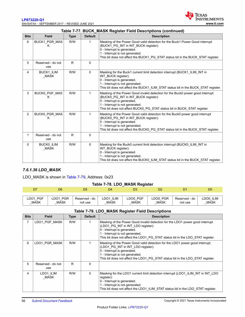
Table 7-77. BUCK_MASK Register Field Descriptions (continued)Bits Field Type Default Description
6 BUCK1_PGR_MASK
R/W 1 Masking of the Power Good valid detection for the Buck1 Power Good interrupt (BUCK1_PG_INT in INT_BUCK register):0 - Interrupt is generated.1 - Interrupt is not generated.This bit does not affect the BUCK1_PG_STAT status bit in the BUCK_STAT register.
5 Reserved - do not use
R 0
4 BUCK1_ILIM_MASK
R/W 0 Masking for the Buck1 current limit detection interrupt (BUCK1_ILIM_INT in INT_BUCK register):0 - Interrupt is generated.1 - Interrupt is not generated.This bit does not affect the BUCK1_ILIM_STAT status bit in the BUCK_STAT register.
3 BUCK0_PGF_MASK
R/W 1 Masking of the Power Good invalid detection for the Buck0 power good interrupt (BUCK0_PG_INT in INT_BUCK register):0 - Interrupt is generated.1 - Interrupt is not generated.This bit does not affect BUCK0_PG_STAT status bit in BUCK_STAT register.
2 BUCK0_PGR_MASK
R/W 1 Masking of the Power Good valid detection for the Buck0 power good interrupt (BUCK0_PG_INT in INT_BUCK register):0 - Interrupt is generated.1 - Interrupt is not generated.This bit does not affect the BUCK0_PG_STAT status bit in the BUCK_STAT register.
1 Reserved - do not use
R 0
0 BUCK0_ILIM_MASK
R/W 0 Masking for the Buck0 current limit detection interrupt (BUCK0_ILIM_INT in INT_BUCK register):0 - Interrupt is generated.1 - Interrupt is not generated.This bit does not affect the BUCK0_ILIM_STAT status bit in the BUCK_STAT register.
7.6.1.36 LDO_MASK
LDO_MASK is shown in Table 7-79, Address: 0x23
Table 7-78. LDO_MASK RegisterD7 D6 D5 D4 D3 D2 D1 D0
LDO1_PGF_MASK
LDO1_PGR_MASK
Reserved - do not use
LDO1_ILIM_MASK
LDO0_PGF_MASK
LDO0_PGR_MASK
Reserved - do not use
LDO0_ILIM_MASK
Table 7-79. LDO_MASK Register Field DescriptionsBits Field Type Default Description
7 LDO1_PGF_MASK R/W 1 Masking of the Power Good invalid detection for the LDO1 power good interrupt (LDO1_PG_INT in INT_LDO register):0 - Interrupt is generated.1 - Interrupt is not generated.This bit does not affect the LDO1_PG_STAT status bit in the LDO_STAT register.
6 LDO1_PGR_MASK R/W 1 Masking of the Power Good valid detection for the LDO1 power good interrupt (LDO1_PG_INT in INT_LDO register):0 - Interrupt is generated.1 - Interrupt is not generated.This bit does not affect the LDO1_PG_STAT status bit in the LDO_STAT register.
5 Reserved - do not use
R 0
4 LDO1_ILIM_MASK
R/W 0 Masking for the LDO1 current limit detection interrupt (LDO1_ILIM_INT in INT_LDO register):0 - Interrupt is generated.1 - Interrupt is not generated.This bit does not affect the LDO1_ILIM_STAT status bit in the LDO_STAT register.
LP873220-Q1SNVSAT4A – SEPTEMBER 2017 – REVISED JUNE 2021 www.ti.com
56 Submit Document Feedback Copyright © 2021 Texas Instruments Incorporated
Product Folder Links: LP873220-Q1
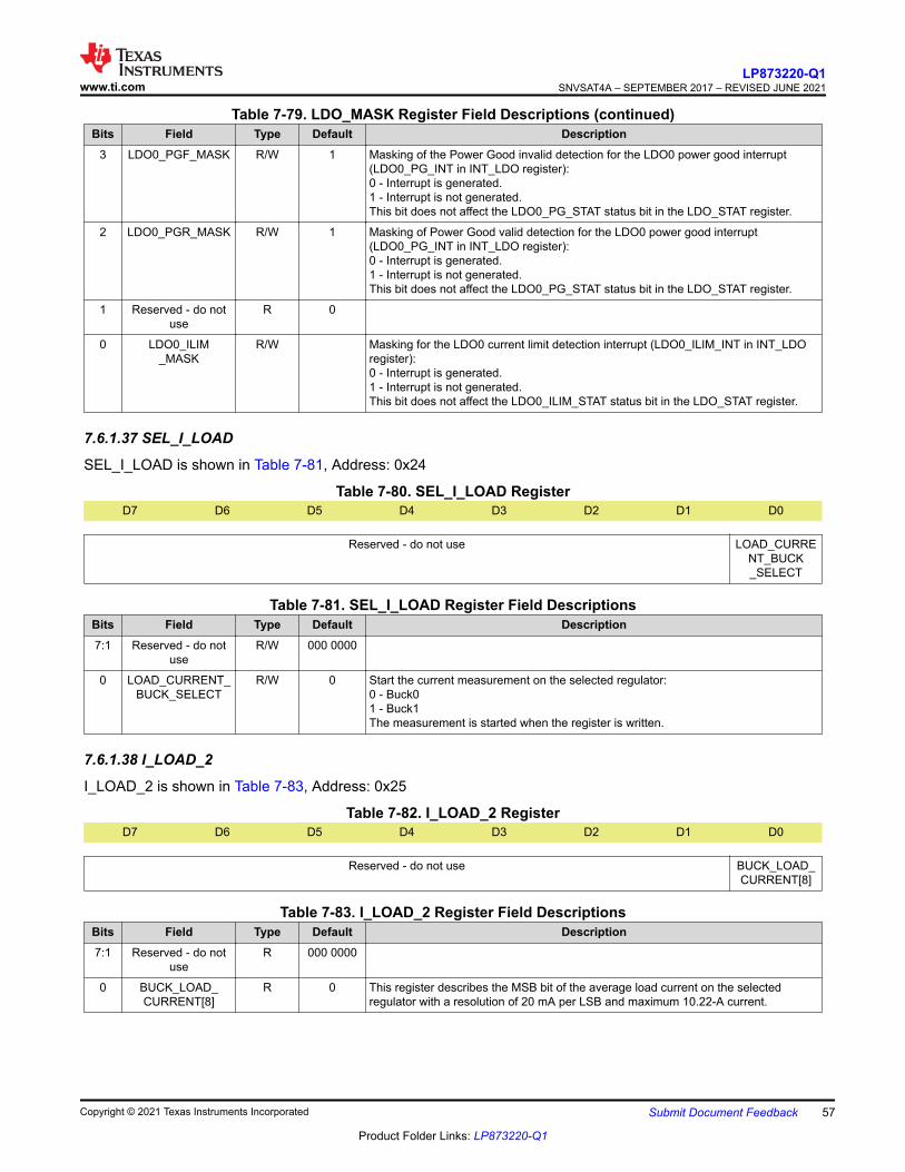
Table 7-79. LDO_MASK Register Field Descriptions (continued)Bits Field Type Default Description
3 LDO0_PGF_MASK R/W 1 Masking of the Power Good invalid detection for the LDO0 power good interrupt (LDO0_PG_INT in INT_LDO register):0 - Interrupt is generated.1 - Interrupt is not generated.This bit does not affect the LDO0_PG_STAT status bit in the LDO_STAT register.
2 LDO0_PGR_MASK R/W 1 Masking of Power Good valid detection for the LDO0 power good interrupt (LDO0_PG_INT in INT_LDO register):0 - Interrupt is generated.1 - Interrupt is not generated.This bit does not affect the LDO0_PG_STAT status bit in the LDO_STAT register.
1 Reserved - do not use
R 0
0 LDO0_ILIM_MASK
R/W Masking for the LDO0 current limit detection interrupt (LDO0_ILIM_INT in INT_LDO register):0 - Interrupt is generated.1 - Interrupt is not generated.This bit does not affect the LDO0_ILIM_STAT status bit in the LDO_STAT register.
7.6.1.37 SEL_I_LOAD
SEL_I_LOAD is shown in Table 7-81, Address: 0x24
Table 7-80. SEL_I_LOAD RegisterD7 D6 D5 D4 D3 D2 D1 D0
Reserved - do not use LOAD_CURRENT_BUCK_SELECT
Table 7-81. SEL_I_LOAD Register Field DescriptionsBits Field Type Default Description7:1 Reserved - do not
useR/W 000 0000
0 LOAD_CURRENT_BUCK_SELECT
R/W 0 Start the current measurement on the selected regulator:0 - Buck01 - Buck1The measurement is started when the register is written.
7.6.1.38 I_LOAD_2
I_LOAD_2 is shown in Table 7-83, Address: 0x25
Table 7-82. I_LOAD_2 RegisterD7 D6 D5 D4 D3 D2 D1 D0
Reserved - do not use BUCK_LOAD_CURRENT[8]
Table 7-83. I_LOAD_2 Register Field DescriptionsBits Field Type Default Description7:1 Reserved - do not
useR 000 0000
0 BUCK_LOAD_CURRENT[8]
R 0 This register describes the MSB bit of the average load current on the selected regulator with a resolution of 20 mA per LSB and maximum 10.22-A current.
www.ti.comLP873220-Q1
SNVSAT4A – SEPTEMBER 2017 – REVISED JUNE 2021
Copyright © 2021 Texas Instruments Incorporated Submit Document Feedback 57
Product Folder Links: LP873220-Q1

7.6.1.39 I_LOAD_1
I_LOAD_1 is shown in Table 7-85, Address: 0x26
Table 7-84. I_LOAD_1 RegisterD7 D6 D5 D4 D3 D2 D1 D0
BUCK_LOAD_CURRENT[7:0]
Table 7-85. I_LOAD_1 Register Field DescriptionsBits Field Type Default Description7:0 BUCK_LOAD_
CURRENT[7:0]R 0000 0000 This register describes 8 LSB bits of the average load current on the selected
regulator with a resolution of 20 mA per LSB and maximum 10.22-A current.
LP873220-Q1SNVSAT4A – SEPTEMBER 2017 – REVISED JUNE 2021 www.ti.com
58 Submit Document Feedback Copyright © 2021 Texas Instruments Incorporated
Product Folder Links: LP873220-Q1

8 Application and ImplementationNote
Information in the following applications sections is not part of the TI component specification, and TI does not warrant its accuracy or completeness. TI’s customers are responsible for determining suitability of components for their purposes. Customers should validate and test their design implementation to confirm system functionality.
8.1 Application InformationThe LP873220-Q1 is a power management unit including two step-down regulators, two linear regulators, and two general-purpose digital output signals.
8.2 Typical Application
SW_B0VIN_B0
VIN_B1
VANA
VIN
FB_B0
VOUT_B0
LOAD
SDA
SCL
nINT
CLKIN (GPO2)
GNDs
EN
GPO
SW_B1
FB_B1
VOUT_B1
LOAD
PGOOD
VOUT_LDO1
VOUT_LDO0
VIN_LDO0
VIN_LDO1
VOUT_LDO0
VOUT_LDO1
Copyright © 2017, Texas Instruments Incorporated
COUT_BUCK0
COUT_BUCK1
COUT_LDO1COUT_LDO0
CIN_LDO1CIN_LDO0
CIN_BUCK0 CIN_BUCK1
CANA
L0
L1
Figure 8-1. LP873220-Q1 Typical Application
8.2.1 Design Requirements8.2.1.1 Inductor Selection
The inductors L0 and L1 are shown in the Section 8.2. The inductance and DCR of the inductor affects the control loop of the buck regulator. TI recommends using inductors similar to those listed in Table 8-1. Pay attention to the saturation current and temperature rise current of the inductor. Check that the saturation current is higher than the peak current limit and the temperature rise current is higher than the maximum expected rms output current. The minimum effective inductance to ensure good performance is 0.22 μH at maximum peak output current over the operating temperature range. DC resistance of the inductor must be less than 0.05 Ω for good efficiency at high-current conditions. The inductor AC loss also affects conversion efficiency. Higher Q factor at switching frequency usually gives better efficiency at light load to middle load. Shielded inductors are preferred, as they radiate less noise.
Table 8-1. Recommended Inductors
MANUFACTURER PART NUMBER VALUE DIMENSIONS L × W × H (mm)RATED DC CURRENT
ISAT maximum (typical) /ITEMP maximum (typical) (A)
DCRtypical / maximum
(mΩ)
TOKO DFE252012PD-R47M
0.47 µH (20%) 2.5 × 2 × 1.2 5.2 (–) / 4 (–)(1) — / 27
www.ti.comLP873220-Q1
SNVSAT4A – SEPTEMBER 2017 – REVISED JUNE 2021
Copyright © 2021 Texas Instruments Incorporated Submit Document Feedback 59
Product Folder Links: LP873220-Q1
Table 8-1. Recommended Inductors (continued)
MANUFACTURER PART NUMBER VALUE DIMENSIONS L × W × H (mm)RATED DC CURRENT
ISAT maximum (typical) /ITEMP maximum (typical) (A)
DCRtypical / maximum
(mΩ)
Tayo Yuden MDMK2020TR47MMV
0.47 µH (20%) 2 × 2 ×1.2 4.2 (4.8) / 2.3 (2.45) 40 / 46
(1) Operating temperature range is up to 125°C including self temperature rise.
8.2.1.2 Buck Input Capacitor Selection
The input capacitors CIN_BUCK0 and CIN_BUCK1 are shown in the Section 8.2. A ceramic input bypass capacitor of 10 μF is required for each phase of the regulator. Place the input capacitor as close as possible to the VIN_Bx pin and PGND_Bx pin of the device. A larger value or higher voltage rating improves the input voltage filtering. Use X7R type of capacitors, not Y5V or F. Also, the DC bias characteristics capacitors must be considered. The minimum effective input capacitance to ensure good performance is 1.9 μF per buck input at maximum input voltage including tolerances, ambient temperature range, and aging (assuming at least 22 μF of additional capacitance is common for all the power input pins on the system power rail). See Table 8-2.
The input filter capacitor supplies current to the high-side FET switch in the first half of each cycle and reduces voltage ripple imposed on the input power source. The low ESR of the ceramic capacitor provides the best noise filtering of the input voltage spikes due to this rapidly changing current. Select an input filter capacitor with sufficient ripple current rating. In addition, ferrite can be used in front of the input capacitor to reduce the EMI.
Table 8-2. Recommended Buck Input Capacitor (X7R Dielectric)MANUFACTURER PART NUMBER VALUE CASE SIZE DIMENSIONS L × W × H
(mm) VOLTAGE RATING
Murata GCM21BR71A106KE22 10 µF (10%) 0805 2 × 1.25 × 1.25 10 V
8.2.1.3 Buck Output Capacitor Selection
The output capacitor COUT_BUCK0 and COUT_BUCK1 are shown in Section 8.2. A ceramic local output capacitor of 22 μF is required per phase. Use ceramic capacitors, X7R type; do not use Y5V or F. DC bias voltage characteristics of ceramic capacitors must be considered. The output filter capacitor smooths out current flow from the inductor to the load, which helps maintain a steady output voltage during transient load changes and reduces output voltage ripple. These capacitors must be selected with sufficient capacitance and sufficiently low ESR and ESL to perform these functions. The minimum effective output capacitance to ensure good performance is 10 μF per phase, including the DC voltage rolloff, tolerances, aging, and temperature effects.
The output voltage ripple is caused by the charging and discharging of the output capacitor and due to its RESR. The RESR is frequency dependent (and temperature dependent); ensure the value used for selection process is at the switching frequency of the part. See Table 8-3.
POL capacitors can be used to improve load transient performance and to decrease the ripple voltage. A higher output capacitance improves the load step behavior, reduces the output voltage ripple, and decreases the PFM switching frequency. However, output capacitance higher than 150 μF per phase is not necessarily of any benefit. The output capacitor may be the limiting factor in the output voltage ramp, see Section 6 for maximum output capacitance for different slew-rate settings. For large output capacitors, the output voltage might be slower than the programmed ramp rate at voltage transitions, because of the higher energy stored on the output capacitance. Also at start-up, the time required to charge the output capacitor to target value might be longer. At shutdown, the output voltage is discharged to a 0.6 V level using forced-PWM operation. This can increase the input voltage if the load current is small and the output capacitor is large compared to input capacitor. Below the 0.6 V level, the output capacitor is discharged by the internal discharge resistor, and with large capacitor more time is required to settle VOUT down as a consequence of the increased time constant.
Table 8-3. Recommended Buck Output Capacitors (X7R Dielectric)MANUFACTURER PART NUMBER VALUE CASE SIZE DIMENSIONS L × W × H
(mm)VOLTAGE RATING
Murata GCM31CR71A226KE02 22 µF (10%) 1206 3.2 × 1.6 × 1.6 10 V
LP873220-Q1SNVSAT4A – SEPTEMBER 2017 – REVISED JUNE 2021 www.ti.com
60 Submit Document Feedback Copyright © 2021 Texas Instruments Incorporated
Product Folder Links: LP873220-Q1
8.2.1.4 LDO Input Capacitor Selection
The input capacitors CIN_LDO0 and CIN_LDO1 are shown in the Table 8-4. A ceramic input capacitor of 2.2 μF, 6.3 V is sufficient for most applications. Place the input capacitor as close as possible to the VIN_LDOx pin and AGND pin of the device. A larger value or higher voltage rating improves the input voltage filtering. Use X7R type of capacitors, not Y5V or F. DC bias characteristics of capacitors must be considered, the minimum effective input capacitance to ensure good performance is 0.6 μF per LDO input at maximum input voltage including tolerances, ambient temperature range, and aging. See Table 8-4.
Table 8-4. Recommended LDO Input Capacitors (X7R Dielectric)MANUFACTURER PART NUMBER VALUE CASE SIZE DIMENSIONS L × W × H
(mm)VOLTAGE RATING
Murata GCM188R70J225KE22 2.2 µF (10%) 0603 1.6 × 0.8 × 0.8 6.3 V
Murata GCM21BR71C475KA73 4.7 µF (10%) 0805 2 × 1.25 × 1.25 16 V
8.2.1.5 LDO Output Capacitor Selection
The output capacitors COUT_LDO0 and COUT_LDO1 are shown in the Section 8.2. A ceramic output capacitor of minimum 1.0 μF is required. Place the output capacitor as close to the VOUT_LDOx pin and AGND pin of the device as possible. Use X7R type of capacitors, not Y5V or F. DC bias characteristics of capacitors must be considered, the minimum effective output capacitance to ensure good performance is 0.4 μF per LDO input at maximum input voltage including tolerances, ambient temperature range, and aging. See Table 8-5.
Note: the output capcitor requirements excludes any capacitance seen at the point of load and only refers to the capacitance seen close to the device. Additional capacitance placed near the load can be supported, but the end applcation system should be evaluated for stability and to ensure the sequencing requirements are met. The shutdown decay will be longer with higher output capcitance, which can also impact the startup time. Total output capacitance should be kept below 100 µF.
The output capacitance must be smaller than the input capacitance to ensure the stability of the LDO. With a 1-μF output capacitor, TI recommends using at least a 2.2-μF input capacitor; with a 2.2-μF output capacitor at least 4.7-μF input capacitance.
The VANA input is used to supply analog and digital circuits in the device. See Table 8-6 for recommended components from for VANA input supply filtering.
Table 8-5. Recommended LDO Output Capacitors (X7R Dielectric)MANUFACTURER PART NUMBER VALUE CASE SIZE DIMENSIONS L × W × H (mm) VOLTAGE RATING
Murata GCM188R71C105KA64 1 µF (10%) 0603 1.6 × 0.8 × 0.8 16 V
Murata GCM188R70J225KE22 2.2 µF (10%) 0603 1.6 × 0.8 × 0.8 6.3 V
Table 8-6. Recommended Supply Filtering ComponentsMANUFACTURER PART NUMBER VALUE CASE SIZE DIMENSIONS L × W × H (mm) VOLTAGE RATING
Murata GCM155R71C104KA55 100 nF (10%) 0402 1 × 0.5 × 0.5 16 V
Murata GCM188R71C104KA37 100 nF (10%) 0603 1.6 × 0.8 × 0.8 16 V
8.2.2 Detailed Design Procedure
The performance of the LP873220-Q1 device depends greatly on the care taken in designing the printed circuit board (PCB). The use of low-inductance and low serial-resistance ceramic capacitors is strongly recommended, while proper grounding is crucial. Attention must be given to decoupling the power supplies. Decoupling capacitors must be connected close to the device and between the power and ground pins to support high peak currents being drawn from system power rail during turnon of the switching MOSFETs. Keep input and output traces as short as possible, because trace inductance, resistance, and capacitance can become performance limiting items. The separate buck regulator power pins VIN_Bx are not connected together internally. Connect the VIN_Bx power connections together outside the package using power plane construction.
www.ti.comLP873220-Q1
SNVSAT4A – SEPTEMBER 2017 – REVISED JUNE 2021
Copyright © 2021 Texas Instruments Incorporated Submit Document Feedback 61
Product Folder Links: LP873220-Q1

8.2.3 Application Curves
Measurements are done using typical application set up with connections shown in Figure 8-1. Graphs may not reflect the OTP default settings. Unless otherwise specified: V(VIN_Bx) = V(VIN_LDOx) = V(VANA) = 3.7 V, VOUT_Bx = 1 V, VOUT_LDOx = 1 V, TA = 25°C, L = 0.47 µH (TOKO DFE252012PD-R47M), COUT_BUCK = 22 µF , and CPOL_BUCK = 22 µF, COUT_LDO = 1 µF.
Output Current (A)
Eff
icie
ncy (
%)
0.001 0.01 0.1 1 240
50
60
70
80
90
100
D004
Vin=5V, AUTOVin=3.3V, AUTOVin=5V, FPWMVin=3.3V, FPWM
VOUT = 1.8 V
Figure 8-2. Buck Efficiency in PFM/PWM and Forced PWM Mode
Output Current (A)
Eff
icie
ncy (
%)
0.001 0.01 0.1 1 240
50
60
70
80
90
100
D008
Vout=1VVout=1.8VVout=2.5V
VIN = 3.3 V
Figure 8-3. Buck Efficiency in Forced PWM Mode
Output Current (A)
Eff
icie
ncy (
%)
0.001 0.01 0.1 1 240
50
60
70
80
90
100
D012
Vout=1VVout=1.8VVout=2.5V
VIN = 5 V
Figure 8-4. Buck Efficiency in Forced PWM Mode
Output Current (A)
Ou
tpu
t V
olta
ge
(V
)
0 0.5 1 1.5 20.98
0.984
0.988
0.992
0.996
1
1.004
1.008
1.012
1.016
1.02
D016
Vin=3.3V, FPWMVin=5.0V, FPWM
VOUT = 1 V
Figure 8-5. Buck Output Voltage vs Load Current in Forced PWM Mode
Output Current (A)
Ou
tpu
t V
olta
ge
(V
)
0 0.1 0.2 0.3 0.4 0.5 0.6 0.7 0.8 0.9 10.98
0.985
0.99
0.995
1
1.005
1.01
1.015
1.02
D019
Vin=3.3V, AUTOVin=5.0V, AUTO
VOUT = 1 V
Figure 8-6. Buck Output Voltage vs Load Current in PFM/PWM Mode
Input Voltage (V)
Ou
tpu
t V
olta
ge
(V
)
2.5 3 3.5 4 4.5 5 5.50.98
0.984
0.988
0.992
0.996
1
1.004
1.008
1.012
1.016
1.02
D021
VOUT = 1 V Load = 1 A
Figure 8-7. Buck Output Voltage vs Input Voltage in PWM Mode
LP873220-Q1SNVSAT4A – SEPTEMBER 2017 – REVISED JUNE 2021 www.ti.com
62 Submit Document Feedback Copyright © 2021 Texas Instruments Incorporated
Product Folder Links: LP873220-Q1

Temperature (qC)
Ou
tpu
t V
olta
ge
(V
)
-40 -20 0 20 40 60 80 100 120 1400.98
0.985
0.99
0.995
1
1.005
1.01
1.015
1.02
D023
PFMPWM
Load = 1 A (PWM) and 0.1 A (PFM)
Figure 8-8. Buck Output Voltage vs Temperature
Slew-rate = 10 mV/µs ILOAD = 0 A VOUT = 1 V
Figure 8-9. Buck Start-Up With EN1, Forced PWM Mode
Slew-rate = 10 mV/µs RLOAD = 1 Ω VOUT = 1 V
Figure 8-10. Buck Start-Up with EN1, Forced PWM Mode
Slew-rate = 10 mV/µs RLOAD = 1 Ω VOUT = 1 V
Figure 8-11. Buck Shutdown With EN1, Forced PWM Mode
IOUT = 10 mA
Figure 8-12. Buck Output Voltage Ripple, PFM Mode
IOUT = 200 mA
Figure 8-13. Buck Output Voltage Ripple, Forced PWM Mode
www.ti.comLP873220-Q1
SNVSAT4A – SEPTEMBER 2017 – REVISED JUNE 2021
Copyright © 2021 Texas Instruments Incorporated Submit Document Feedback 63
Product Folder Links: LP873220-Q1

Figure 8-14. Buck Transient From PFM-to-PWM Mode
Figure 8-15. Buck Transient From PWM-to-PFM Mode
IOUT = 0.1 A → 2 A → 0.1 A
TR = TF = 400 ns
Figure 8-16. Buck Transient Load Step Response, AUTO Mode
IOUT = 0.1 A → 2 A → 0.1 A
TR = TF = 400 ns
Figure 8-17. Buck Transient Load Step Response, Forced PWM Mode
VOUT(200mV/div)
Time (400 µs/div)
Figure 8-18. Buck VOUT Transition from 0.6 V to 1.4 V With Different Slew Rate Settings
VOUT(200mV/div)
Time (400 µs/div)
Figure 8-19. Buck VOUT Transition from 1.4 V to 0.6 V With Different Slew Rate Settings
LP873220-Q1SNVSAT4A – SEPTEMBER 2017 – REVISED JUNE 2021 www.ti.com
64 Submit Document Feedback Copyright © 2021 Texas Instruments Incorporated
Product Folder Links: LP873220-Q1

Figure 8-20. Buck Start-Up With Short on Output Output Current (mA)
Outp
ut
Voltag
e (
V)
0 50 100 150 200 250 3000.98
0.985
0.99
0.995
1
1.005
1.01
1.015
1.02
D050
Vin=3.3VVin=5V
VOUT = 1 V
Figure 8-21. LDO Output Voltage vs Load Current
Input Voltage (V)
Outp
ut
Voltag
e (
V)
2.5 3 3.5 4 4.5 5 5.50.98
0.985
0.99
0.995
1
1.005
1.01
1.015
1.02
D051
VOUT = 1 V Load = 200 mA
Figure 8-22. LDO Output Voltage vs Input Voltage
Temperature (qC)
Ou
tpu
t V
olta
ge
(V
)
-40 -20 0 20 40 60 80 100 120 1400.98
0.985
0.99
0.995
1
1.005
1.01
1.015
1.02
D052
VOUT = 1 V Load = 200 mA
Figure 8-23. LDO Output Voltage vs Temperature
ILOAD = 0 A VOUT = 1 V
Figure 8-24. LDO Start-UpRLOAD = 3.3 Ω VOUT = 1 V
Figure 8-25. LDO Start-Up
www.ti.comLP873220-Q1
SNVSAT4A – SEPTEMBER 2017 – REVISED JUNE 2021
Copyright © 2021 Texas Instruments Incorporated Submit Document Feedback 65
Product Folder Links: LP873220-Q1

ILOAD = 0 A VOUT = 1 V
Figure 8-26. LDO ShutdownIOUT = 0 A → 0.3 A → 0 A TR = TF = 1 µs
Figure 8-27. LDO Transient Load Step Response
Figure 8-28. LDO VOUT Transition from 1.8 V to 1.2 V
Figure 8-29. LDO VOUT Transition from 1.2 V to 1.8 V
Start-up delay is 500 µs
Figure 8-30. LDO Start-Up With Short on Output
9 Power Supply RecommendationsThe device is designed to operate from an input voltage supply range between 2.8 V and 5.5 V. The VANA input and VIN_Bx buck inputs must be connected together, and they must use the same input supply. This input supply must be well regulated and able to withstand maximum input current and maintain stable voltage without voltage drop even at load transition condition. The resistance of the input supply rail must be low enough that the input current transient does not cause too high a drop in the LP873220-Q1 supply voltage that can cause false UVLO fault triggering. If the input supply is located more than a few inches from the LP873220-Q1, additional bulk capacitance may be required in addition to the ceramic bypass capacitors. The VIN_LDOx LDO input supply voltage range is 2.5 V to 5.5 V and can be higher or lower than VANA supply voltage.
LP873220-Q1SNVSAT4A – SEPTEMBER 2017 – REVISED JUNE 2021 www.ti.com
66 Submit Document Feedback Copyright © 2021 Texas Instruments Incorporated
Product Folder Links: LP873220-Q1

10 Layout10.1 Layout GuidelinesThe high frequency and large switching currents of the LP873220-Q1 make the choice of layout important. Good power supply results only occur when care is given to proper design and layout. Layout affects noise pickup and generation and can cause a good design to perform with less-than-expected results. With a range of output currents from milliamps to several amps, good power supply layout is much more difficult than most general PCB design. Use the following steps as a reference to ensure the device is stable and maintains proper voltage and current regulation across its intended operating voltage and current range.
1. Place CIN as close as possible to the VIN_Bx pin and the PGND_Bx pin. Route the VIN trace wide and thick to avoid IR drops. The trace between the positive node of the input capacitor and the VIN_Bx pins of LP873220-Q1, as well as the trace between the negative node of the input capacitor and the power PGND_Bx pins, must be kept as short as possible. The input capacitance provides a low-impedance voltage source for the switching converter. The inductance of the connection is the most important parameter of a local decoupling capacitor — parasitic inductance on these traces must be kept as small as possible for proper device operation. The parasitic inductance can be reduced by using a ground plane as close as possible to the top layer by using thin dielectric layer between the top layer and the ground plane.
2. The output filter, consisting of L and COUT, converts the switching signal at SW_Bx to the noiseless output voltage. The output filter must be placed as close as possible to the device, keeping the switch node small for best EMI behavior. Route the traces between the output capacitors of the LP873220-Q1 and the input capacitors of the load direct and wide to avoid losses due to the IR drop.
3. Input for analog blocks (VANA and AGND) must be isolated from noisy signals. Connect VANA directly to a quiet system voltage node and AGND to a quiet ground point where no IR drop occurs. Place the decoupling capacitor as close as possible to the VANA pin.
4. If remote voltage sensing can be used for the load, connect the LP873220-Q1 feedback pins FB_Bx to the respective sense pins on the load capacitor. The sense lines are susceptible to noise. They must be kept away from noisy signals such as PGND_Bx, VIN_Bx, and SW_Bx, as well as high bandwidth signals such as the I2C. Avoid both capacitive and inductive coupling by keeping the sense lines short and direct, and close to each other. Run the lines in a quiet layer. Isolate them from noisy signals by a voltage or ground plane if possible. If series resistors are used for load current measurement, place them after connection of the voltage feedback.
5. PGND_Bx, VIN_Bx and SW_Bx must be routed on thick layers. They must not surround inner signal layers which are not able to withstand interference from noisy PGND_Bx, VIN_Bx and SW_Bx.
6. LDO performance (PSRR, noise, and transient response) depend on the layout of the PCB. Best performance is achieved by placing CIN and COUT as close to the LP873220-Q1 device as practical. The ground connections for CIN and COUT must be back to the LP873220-Q1 AGND with as wide and as short of a copper trace as is practical and with multiple vias if routing is done on other layer. Avoid connections using long trace lengths, narrow trace widths, or connection through small via. These add parasitic inductances and resistance that results in inferior performance, especially during transient conditions.
Due to the small package of this converter and the overall small solution size, the thermal performance of the PCB layout is important. Many system-dependent issues such as thermal coupling, airflow, added heat sinks and convection surfaces, and the presence of other heat-generating components affect the power dissipation limits of a given component. Proper PCB layout, focusing on thermal performance, results in lower die temperatures. Wide power traces can sink dissipated heat. This can be improved further on multi-layer PCB designs with vias to different planes. This results in reduced junction-to-ambient (RθJA) and junction-to-board (RθJB) thermal resistances, thereby reducing the device junction temperature, TJ. TI strongly recommends performance of a careful system-level 2D or full 3D dynamic thermal analysis at the beginning product design process by using a thermal modeling analysis software.
www.ti.comLP873220-Q1
SNVSAT4A – SEPTEMBER 2017 – REVISED JUNE 2021
Copyright © 2021 Texas Instruments Incorporated Submit Document Feedback 67
Product Folder Links: LP873220-Q1

10.2 Layout Example
AGND
1
29
VO
UT
_L
DO
0
2
FB
_B
0
3
FB
_B
1
7
VO
UT
_L
DO
1
4
AG
ND
5
VA
NA
6
EN
15
PG
ND
_B
1
16
PG
ND
_B
1
17
SC
L
21
PG
ND
_B
0
18
SD
A
19
SG
ND
20
PG
ND
_B
0
22 SW_B0
23 SW_B0
24 VIN_B0
28 VIN_LDO0
25 VIN_B0
26 GPO
27 PGOOD
8VIN_LDO1
9nINT
10CLKIN
14SW_B1
11VIN_B1
12VIN_B1
13SW_B1A
GN
D
AGND
AGNDAGND
AGND
VOUT0 VOUT1
VOUT2 VOUT3
VIN
VIN
VINGND VIN GND
VIN
CIN0 CIN1
CIN2 CIN3
L0 L1
COUT0 COUT1
COUT2
COUT3
CANA
GND
Figure 10-1. LP873220-Q1 Board Layout
LP873220-Q1SNVSAT4A – SEPTEMBER 2017 – REVISED JUNE 2021 www.ti.com
68 Submit Document Feedback Copyright © 2021 Texas Instruments Incorporated
Product Folder Links: LP873220-Q1

11 Device and Documentation Support11.1 Device Support11.1.1 Third-Party Products Disclaimer
TI'S PUBLICATION OF INFORMATION REGARDING THIRD-PARTY PRODUCTS OR SERVICES DOES NOT CONSTITUTE AN ENDORSEMENT REGARDING THE SUITABILITY OF SUCH PRODUCTS OR SERVICES OR A WARRANTY, REPRESENTATION OR ENDORSEMENT OF SUCH PRODUCTS OR SERVICES, EITHER ALONE OR IN COMBINATION WITH ANY TI PRODUCT OR SERVICE.
11.2 Receiving Notification of Documentation UpdatesTo receive notification of documentation updates, navigate to the device product folder on ti.com. In the upper right corner, click on Alert me to register and receive a weekly digest of any product information that has changed. For change details, review the revision history included in any revised document.
11.3 Support ResourcesTI E2E™ support forums are an engineer's go-to source for fast, verified answers and design help — straight from the experts. Search existing answers or ask your own question to get the quick design help you need.
Linked content is provided "AS IS" by the respective contributors. They do not constitute TI specifications and do not necessarily reflect TI's views; see TI's Terms of Use.
11.4 TrademarksTI E2E™ is a trademark of Texas Instruments.All trademarks are the property of their respective owners.11.5 Electrostatic Discharge Caution
This integrated circuit can be damaged by ESD. Texas Instruments recommends that all integrated circuits be handled with appropriate precautions. Failure to observe proper handling and installation procedures can cause damage.ESD damage can range from subtle performance degradation to complete device failure. Precision integrated circuits may be more susceptible to damage because very small parametric changes could cause the device not to meet its published specifications.
11.6 GlossaryTI Glossary This glossary lists and explains terms, acronyms, and definitions.
12 Mechanical, Packaging, and Orderable InformationThe following pages include mechanical, packaging, and orderable information. This information is the most current data available for the designated devices. This data is subject to change without notice and revision of this document. For browser-based versions of this data sheet, refer to the left-hand navigation.
www.ti.comLP873220-Q1
SNVSAT4A – SEPTEMBER 2017 – REVISED JUNE 2021
Copyright © 2021 Texas Instruments Incorporated Submit Document Feedback 69
Product Folder Links: LP873220-Q1

PACKAGE OPTION ADDENDUM
www.ti.com 26-Sep-2022
PACKAGING INFORMATION
Orderable Device Status(1)
Package Type PackageDrawing
Pins PackageQty
Eco Plan(2)
Lead finish/Ball material
(6)
MSL Peak Temp(3)
Op Temp (°C) Device Marking(4/5)
Samples
LP873220RHDRQ1 ACTIVE VQFN RHD 28 3000 RoHS & Green NIPDAU | SN Level-2-260C-1 YEAR -40 to 125 LP873220-Q1
Samples
LP873220RHDTQ1 ACTIVE VQFN RHD 28 250 RoHS & Green NIPDAU | SN Level-2-260C-1 YEAR -40 to 125 LP873220-Q1
Samples
(1) The marketing status values are defined as follows:ACTIVE: Product device recommended for new designs.LIFEBUY: TI has announced that the device will be discontinued, and a lifetime-buy period is in effect.NRND: Not recommended for new designs. Device is in production to support existing customers, but TI does not recommend using this part in a new design.PREVIEW: Device has been announced but is not in production. Samples may or may not be available.OBSOLETE: TI has discontinued the production of the device.
(2) RoHS: TI defines "RoHS" to mean semiconductor products that are compliant with the current EU RoHS requirements for all 10 RoHS substances, including the requirement that RoHS substancedo not exceed 0.1% by weight in homogeneous materials. Where designed to be soldered at high temperatures, "RoHS" products are suitable for use in specified lead-free processes. TI mayreference these types of products as "Pb-Free".RoHS Exempt: TI defines "RoHS Exempt" to mean products that contain lead but are compliant with EU RoHS pursuant to a specific EU RoHS exemption.Green: TI defines "Green" to mean the content of Chlorine (Cl) and Bromine (Br) based flame retardants meet JS709B low halogen requirements of <=1000ppm threshold. Antimony trioxide basedflame retardants must also meet the <=1000ppm threshold requirement.
(3) MSL, Peak Temp. - The Moisture Sensitivity Level rating according to the JEDEC industry standard classifications, and peak solder temperature.
(4) There may be additional marking, which relates to the logo, the lot trace code information, or the environmental category on the device.
(5) Multiple Device Markings will be inside parentheses. Only one Device Marking contained in parentheses and separated by a "~" will appear on a device. If a line is indented then it is a continuationof the previous line and the two combined represent the entire Device Marking for that device.
(6) Lead finish/Ball material - Orderable Devices may have multiple material finish options. Finish options are separated by a vertical ruled line. Lead finish/Ball material values may wrap to twolines if the finish value exceeds the maximum column width.
Important Information and Disclaimer:The information provided on this page represents TI's knowledge and belief as of the date that it is provided. TI bases its knowledge and belief on informationprovided by third parties, and makes no representation or warranty as to the accuracy of such information. Efforts are underway to better integrate information from third parties. TI has taken andcontinues to take reasonable steps to provide representative and accurate information but may not have conducted destructive testing or chemical analysis on incoming materials and chemicals.TI and TI suppliers consider certain information to be proprietary, and thus CAS numbers and other limited information may not be available for release.
In no event shall TI's liability arising out of such information exceed the total purchase price of the TI part(s) at issue in this document sold by TI to Customer on an annual basis.
Addendum-Page 1

PACKAGE OPTION ADDENDUM
www.ti.com 26-Sep-2022
OTHER QUALIFIED VERSIONS OF LP873220-Q1 :
• Catalog : LP873220
NOTE: Qualified Version Definitions:
• Catalog - TI's standard catalog product
Addendum-Page 2

PACKAGE MATERIALS INFORMATION
www.ti.com 9-Aug-2022
TAPE AND REEL INFORMATION
Reel Width (W1)
REEL DIMENSIONS
A0B0K0W
Dimension designed to accommodate the component lengthDimension designed to accommodate the component thicknessOverall width of the carrier tapePitch between successive cavity centers
Dimension designed to accommodate the component width
TAPE DIMENSIONS
K0 P1
B0 W
A0Cavity
QUADRANT ASSIGNMENTS FOR PIN 1 ORIENTATION IN TAPE
Pocket Quadrants
Sprocket Holes
Q1 Q1Q2 Q2
Q3 Q3Q4 Q4 User Direction of Feed
P1
ReelDiameter
*All dimensions are nominal
Device PackageType
PackageDrawing
Pins SPQ ReelDiameter
(mm)
ReelWidth
W1 (mm)
A0(mm)
B0(mm)
K0(mm)
P1(mm)
W(mm)
Pin1Quadrant
LP873220RHDRQ1 VQFN RHD 28 3000 330.0 12.4 5.25 5.25 1.1 8.0 12.0 Q2
LP873220RHDTQ1 VQFN RHD 28 250 180.0 12.4 5.25 5.25 1.1 8.0 12.0 Q2
Pack Materials-Page 1
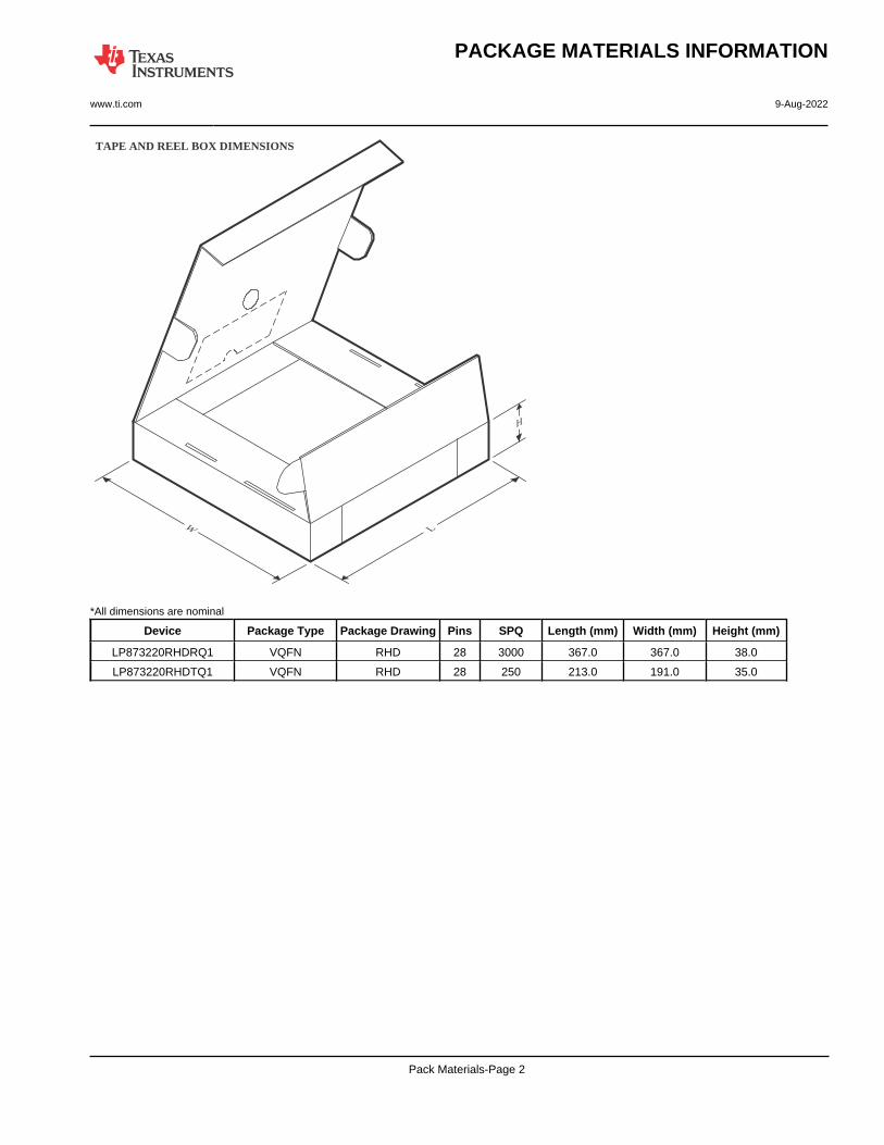
PACKAGE MATERIALS INFORMATION
www.ti.com 9-Aug-2022
TAPE AND REEL BOX DIMENSIONS
Width (mm)
W L
H
*All dimensions are nominal
Device Package Type Package Drawing Pins SPQ Length (mm) Width (mm) Height (mm)
LP873220RHDRQ1 VQFN RHD 28 3000 367.0 367.0 38.0
LP873220RHDTQ1 VQFN RHD 28 250 213.0 191.0 35.0
Pack Materials-Page 2
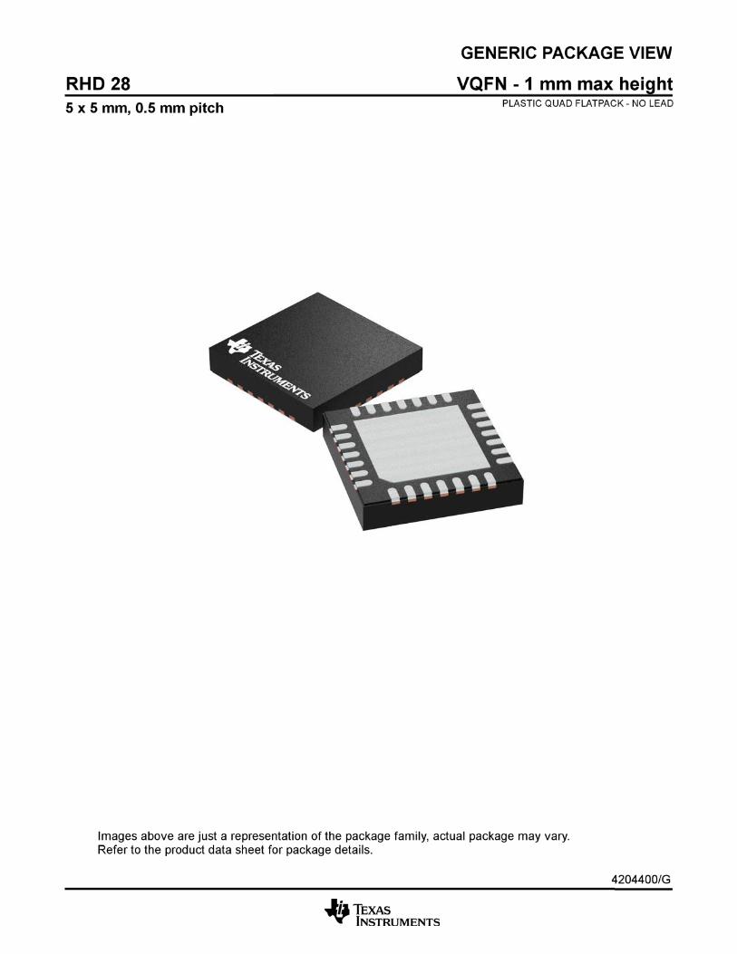

A A
www.ti.com
PACKAGE OUTLINE
C
28X 0.30.2
3.4 0.1
28X 0.650.45
1 MAX
(0.2) TYP
0.050.00
24X 0.5
4X3
A 5.14.9
B
5.14.9
0.1 MIN
(0.05)
VQFN - 1 mm max heightRHD0028WPLASTIC QUAD FLATPACK - NO LEAD
4222120/B 02/2018
PIN 1 INDEX AREA
0.08
SEATING PLANE
1
715
21
8 14
28 22(OPTIONAL)
PIN 1 ID0.1 C A B0.05
EXPOSEDTHERMAL PAD
SYMM
SYMM
NOTES: 1. All linear dimensions are in millimeters. Any dimensions in parenthesis are for reference only. Dimensioning and tolerancing per ASME Y14.5M. 2. This drawing is subject to change without notice. 3. The package thermal pad must be soldered to the printed circuit board for thermal and mechanical performance.
SCALE 2.500
A-A 25.000SECTION A-ATYPICAL

www.ti.com
EXAMPLE BOARD LAYOUT
0.07 MINALL AROUND
0.07 MAXALL AROUND
28X (0.25)
28X (0.75)
( 0.2) TYPVIA
(R0.05) TYP
(1.45)
(4.65)
(4.65)
(0.5) TYP
( 3.4)
(1.45)
VQFN - 1 mm max heightRHD0028WPLASTIC QUAD FLATPACK - NO LEAD
4222120/B 02/2018
SYMM
1
7
8 14
15
21
2228
SYMM
LAND PATTERN EXAMPLEEXPOSED METAL SHOWN
SCALE:15X
NOTES: (continued) 4. This package is designed to be soldered to a thermal pad on the board. For more information, see Texas Instruments literature number SLUA271 (www.ti.com/lit/slua271).
SOLDER MASKOPENING
METAL UNDERSOLDER MASK
SOLDER MASKDEFINED
EXPOSEDMETAL
METAL EDGE
SOLDER MASKOPENING
SOLDER MASK DETAILS
NON SOLDER MASKDEFINED
(PREFERRED)
EXPOSEDMETAL
www.ti.com
EXAMPLE STENCIL DESIGN
28X (0.75)
28X (0.25)
24X (0.5)
(4.65)
(4.65)
4X ( 1.47)
(0.84)TYP
(0.84) TYP
(R0.05) TYP
VQFN - 1 mm max heightRHD0028WPLASTIC QUAD FLATPACK - NO LEAD
4222120/B 02/2018
NOTES: (continued) 5. Laser cutting apertures with trapezoidal walls and rounded corners may offer better paste release. IPC-7525 may have alternate design recommendations.
SYMM
METALTYP
SOLDER PASTE EXAMPLEBASED ON 0.125 mm THICK STENCIL
EXPOSED PAD
75% PRINTED SOLDER COVERAGE BY AREASCALE:20X
SYMM
1
7
8 14
15
21
2228

IMPORTANT NOTICE AND DISCLAIMERTI PROVIDES TECHNICAL AND RELIABILITY DATA (INCLUDING DATA SHEETS), DESIGN RESOURCES (INCLUDING REFERENCE DESIGNS), APPLICATION OR OTHER DESIGN ADVICE, WEB TOOLS, SAFETY INFORMATION, AND OTHER RESOURCES “AS IS” AND WITH ALL FAULTS, AND DISCLAIMS ALL WARRANTIES, EXPRESS AND IMPLIED, INCLUDING WITHOUT LIMITATION ANY IMPLIED WARRANTIES OF MERCHANTABILITY, FITNESS FOR A PARTICULAR PURPOSE OR NON-INFRINGEMENT OF THIRD PARTY INTELLECTUAL PROPERTY RIGHTS.These resources are intended for skilled developers designing with TI products. You are solely responsible for (1) selecting the appropriate TI products for your application, (2) designing, validating and testing your application, and (3) ensuring your application meets applicable standards, and any other safety, security, regulatory or other requirements.These resources are subject to change without notice. TI grants you permission to use these resources only for development of an application that uses the TI products described in the resource. Other reproduction and display of these resources is prohibited. No license is granted to any other TI intellectual property right or to any third party intellectual property right. TI disclaims responsibility for, and you will fully indemnify TI and its representatives against, any claims, damages, costs, losses, and liabilities arising out of your use of these resources.TI’s products are provided subject to TI’s Terms of Sale or other applicable terms available either on ti.com or provided in conjunction with such TI products. TI’s provision of these resources does not expand or otherwise alter TI’s applicable warranties or warranty disclaimers for TI products.TI objects to and rejects any additional or different terms you may have proposed. IMPORTANT NOTICE
Mailing Address: Texas Instruments, Post Office Box 655303, Dallas, Texas 75265Copyright © 2022, Texas Instruments Incorporated