linear technology - Analog Devices
48
LINEAR TECHNOLOGY LINEAR TECHNOLOGY LINEAR TECHNOL OG Y SEPTEMBER 2005 VOLUME XV NUMBER 3 tor and a buck regulator, which adds complexity with extra filter compo- nents and multiple control loops. The LTC3780 offers a simpler solu- tion with an approach that requires neither cumbersome magnetics nor additional control loops (see Figure 1). This 4-switch controller takes the form of a true synchronous buck or boost, depending on the input voltage. Transitions between modes depend on duty cycle (Figure 2) and are quick and automatic. The controller is versatile, providing three modes of operation, switching frequencies from 200kHz to 400kHz, and output currents from milliamps to tens of amps. The three operating modes permit the designer to choose between efficiency and low , LTC, LT, Burst Mode, OPTI-LOOP, Over-The-Top and PolyPhase are registered trademarks of Linear Technology Cor- poration. Adaptive Power, C-Load, DirectSense, Easy Drive, FilterCAD, Hot Swap, LinearView, Micropower SwitcherCAD, Multimode Dimming, No Latency ΔΣ, No Latency Delta-Sigma, No R SENSE , Operational Filter, PanelProtect, PowerPath, PowerSOT, SmartStart, SoftSpan, Stage Shedding, SwitcherCAD, ThinSOT, UltraFast and VLDO are trademarks of Linear Technology Corporation. Other product names may be trademarks of the companies that manufacture the products. Breakthrough Buck-Boost Controller Provides up to 10A from a Wide 4V–36V Input Range Introduction Many DC/DC converter applications require an output voltage somewhere within a wide range of input volt- ages. An everyday example would be a well-regulated 12V output from an automotive battery input, which has a full charge voltage around 14V and a fluctuating cold crank voltage under 9V. There are a number of traditional solutions to this problem, but all have drawbacks, including low efficiency, limited input voltage range or the use bulky coupled inductors. Some even produce output voltages of polarity opposite to that of the input voltage. A system designer must often decide between an inefficient topology or a scheme that uses both a boost regula- continued on page 3 IN THIS ISSUE… COVER ARTICLE Breakthrough Buck-Boost Controller Provides up to 10A from a Wide 4V–36V Input Range ...........................1 Theo Phillips and Wilson Zhou Issue Highlights ..................................2 Linear Technology in the News….........2 DESIGN FEATURES Dual, 1.4A and 800mA, Buck Regulator for Space-Sensitive Applications .........7 Scott Fritz µPower Precision Dual Op Amp Combines the Advantages of Bipolar and CMOS Amplifiers ..............9 Cheng-Wei Pei and Hengsheng Liu High Voltage Micropower Regulators Thrive in Harsh Environments ..........11 Todd Owen Complete 2-Cell-AA/USB Power Manager in a 4mm × 4mm QFN .........13 G. Thandi Micropower Precision Oscillator Draws Only 60µA at 1MHz ...............17 Albert Huntington New Standalone Linear Li-Ion Battery Chargers .....................20 Alfonso Centuori Monolithic Buck Regulator Operates Down to 1.6V Input; Simplifies Design of 2-Cell NiCd/NiMh Supplies .............22 Gregg Castellucci Supply Tracking and Sequencing at Point-of-Load: Easy Design without the Drawbacks of MOSFETs ..............24 Scott Jackson Versatile Controller Simplifies High Voltage DC/DC Converter Designs ......28 Tom Sheehan Multichannel, 3V and 5V, 16-Bit ADCs Combine High Performance, Speed, Low Power and Small Size ................31 Ringo Lee DESIGN IDEAS ....................................................35–44 (complete list on page 35) New Device Cameos ...........................45 Design Tools......................................47 Sales Offices .....................................48 by Theo Phillips and Wilson Zhou L SW1 SNS + SNS + SNS – R SENSE SW2 A B C D C IN V IN C OUT R1 R2 LTC3780 SNS – V OUT ONLY ONE INDUCTOR SIMPLIFIES LAYOUT AND SAVES SPACE 4-SWITCH BUCK-BOOST TOPOLOGY YIELDS HIGH EFFICIENCY AT HIGH POWER SINGLE SENSE RESISTOR KEEPS EFFICIENCY HIGH Figure 1. Simplified diagram of the LTC3780 topology, showing how the four power switches are connected to the inductor, V IN , V OUT and GND.
-
Upload
khangminh22 -
Category
Documents
-
view
0 -
download
0
Transcript of linear technology - Analog Devices

LINEAR TECHNOLOGYLINEAR TECHNOLOGYLINEAR TECHNOLOGYSEPTEMBER 2005 VOLUME XV NUMBER 3
tor and a buck regulator, which adds complexity with extra filter compo-nents and multiple control loops.
The LTC3780 offers a simpler solu-tion with an approach that requires neither cumbersome magnetics nor additional control loops (see Figure 1). This 4-switch controller takes the form of a true synchronous buck or boost, depending on the input voltage. Transitions between modes depend on duty cycle (Figure 2) and are quick and automatic. The controller is versatile, providing three modes of operation, switching frequencies from 200kHz to 400kHz, and output currents from milliamps to tens of amps. The three operating modes permit the designer to choose between efficiency and low
, LTC, LT, Burst Mode, OPTI-LOOP, Over-The-Top and PolyPhase are registered trademarks of Linear Technology Cor-poration. Adaptive Power, C-Load, DirectSense, Easy Drive, FilterCAD, Hot Swap, LinearView, Micropower SwitcherCAD, Multimode Dimming, No Latency ΔΣ, No Latency Delta-Sigma, No RSENSE, Operational Filter, PanelProtect, PowerPath, PowerSOT, SmartStart, SoftSpan, Stage Shedding, SwitcherCAD, ThinSOT, UltraFast and VLDO are trademarks of Linear Technology Corporation. Other product names may be trademarks of the companies that manufacture the products.
Breakthrough Buck-Boost Controller Provides up to 10A from a Wide 4V–36V Input Range IntroductionMany DC/DC converter applications require an output voltage somewhere within a wide range of input volt-ages. An everyday example would be a well-regulated 12V output from an automotive battery input, which has a full charge voltage around 14V and a fluctuating cold crank voltage under 9V.
There are a number of traditional solutions to this problem, but all have drawbacks, including low efficiency, limited input voltage range or the use bulky coupled inductors. Some even produce output voltages of polarity opposite to that of the input voltage. A system designer must often decide between an inefficient topology or a scheme that uses both a boost regula-
continued on page 3
IN THIS ISSUE…
COVER ARTICLE
Breakthrough Buck-Boost Controller Provides up to 10A from a Wide 4V–36V Input Range ...........................1Theo Phillips and Wilson Zhou
Issue Highlights ..................................2Linear Technology in the News… .........2
DESIGN FEATURES
Dual, 1.4A and 800mA, Buck Regulator for Space-Sensitive Applications .........7Scott Fritz
µPower Precision Dual Op Amp Combines the Advantages of Bipolar and CMOS Amplifiers ..............9Cheng-Wei Pei and Hengsheng Liu
High Voltage Micropower Regulators Thrive in Harsh Environments ..........11Todd Owen
Complete 2-Cell-AA/USB Power Manager in a 4mm × 4mm QFN .........13G. Thandi
Micropower Precision Oscillator Draws Only 60µA at 1MHz ...............17Albert Huntington
New Standalone Linear Li-Ion Battery Chargers .....................20Alfonso Centuori
Monolithic Buck Regulator Operates Down to 1.6V Input; Simplifies Design of 2-Cell NiCd/NiMh Supplies .............22Gregg Castellucci
Supply Tracking and Sequencing at Point-of-Load: Easy Design without the Drawbacks of MOSFETs ..............24Scott Jackson
Versatile Controller Simplifies High Voltage DC/DC Converter Designs ......28Tom Sheehan
Multichannel, 3V and 5V, 16-Bit ADCs Combine High Performance, Speed, Low Power and Small Size ................31Ringo Lee
DESIGN IDEAS ....................................................35–44(complete list on page 35)
New Device Cameos ...........................45
Design Tools ......................................47
Sales Offices .....................................48
by Theo Phillips and Wilson Zhou
L SW1
SNS+
SNS+
SNS–
RSENSE
SW2A
B C
D
CIN
VIN
COUT
R1
R2LTC3780
SNS–
VOUT
ONLY ONE INDUCTOR SIMPLIFIESLAYOUT AND SAVES SPACE
4-SWITCH BUCK-BOOSTTOPOLOGY YIELDS HIGH
EFFICIENCY AT HIGH POWER
SINGLE SENSE RESISTORKEEPS EFFICIENCY HIGH
Figure 1. Simplified diagram of the LTC3780 topology, showing how the four power switches are connected to the inductor, VIN, VOUT and GND.

2 Linear Technology Magazine • September 20052
EDITOR’S PAGE
The LTC3409 is a monolithic synchronous step-down regulator designed specifically to save space, improve battery life and simplify the design of 2-cell-alkaline, NiCd and NiMh powered applications. (Page 22)
The LTC2927 provides simple tracking and sequencing solutions in a tiny footprint, without the drawbacks of series MOSFETs. (Page 24)
The LT3724 is a single-switch DC/DC controller that can be used in medium power step-down, step-up, inverting and SEPIC converter topolo-gies. (Page 28)
High Performance ADCsMany of today’s data acquisition ap-plications require low-power and/or remote sensing capabilities while oc-cupying a minimum amount of board space. Linear Technology introduces a pin-compatible family of 12-bit and 16-bit A/D converters that meet these requirements. (Page 31)
Micropower Op AmpsThe LTC6078 and LTC6079 are dual and quad micropower, preci-sion op amps that combine the low offset and drift of traditional bipolar amplifiers with the low bias current of CMOS amplifiers. They include a combination of features that allow precision performance previously available only through composite amplifiers, manual offset trimming, or calibration.(Page 9)
Precision Silicon OscillatorThe LTC6906 is a monolithic silicon oscillator with significant size, power, cost and environmental sensitivity advantages over other oscillators. It requires only a single external resistor to set the frequency over its full range of 10kHz to 1MHz. (Page 17)
Design Ideas and CameosThe Design Ideas start on page 35, in-cluding a discusion of Ni-based battery chargers and a way to determine the real resistance of a battery.
Issue Highlights
Many DC/DC converter applica-tions require an output voltage somewhere within a wide range
of input voltages. Traditional ap-proaches to this problem can require cumbersome magnetics or additional control loops. The LTC®3780 offers a simpler, much more compact and high performance solution by taking the form of a true synchronous buck or boost, depending on the input voltage. Transitions between modes depend on duty cycle and are quick and automatic.
See our cover article for more about this breakthrough device.
Featured DevicesBelow is a summary of the other de-vices featured in this issue.
Power SolutionsThe LTC3417 is a dual synchronous, step-down, current mode, DC/DC converter designed for medium power applications. It operates from an input voltage between 2.25V and 5.5V and switches at up to 4MHz, making it possible to use low profile capacitors and inductors. (Page 7)
The LT3012 and LT3013 are high voltage micropower regulators designed for industrial and automo-tive environments. They offer an input voltage range of 4V to 80V and minimize power loss by running with quiescent currents of 55µA (LT3012) and 65µA (LT3013). Quiescent current is reduced to just 1µA in shutdown. (Page 11)
The LTC3456 is a complete system power IC that seamlessly manages power flow between an AC wall adapter, USB and 2-AA battery, while complying with USB power standards—all in a 4mm × 4mm QFN package. (Page 13)
The LTC4061 and LTC4062 are specifically designed to charge single-cell lithium-ion batteries from either awall adapter or available USB power. Both devices use constant current/constant voltage algorithms to deliver up to 1A of charge current. (Page 20)
Linear Technology in the News…
Linear Tops $1 BillionOn July 26, Linear Technology Corporation announced financial results for its fiscal year 2005, ending July 3, 2005. According to Lothar Maier, CEO, “Fiscal 2005 was a good year for us in what was generally described as a slow growth environment, and our rate of sales growth was greater than all of our major competitors, allowing us to achieve over $1 billion in revenues for the first time in the Company’s history.”
Products in the NewsLeading Edge… The May 12 edi-tion of EDN featured the LT5527 400MHz to 3.7GHz High Signal Level Downconverting Mixer in the “Leading Edge” section of the magazine. The “Leading Edge” column focuses on what’s hot in the design community. Mixer Times Two… The June issue of Wireless Design & De-velopment featured the LT5527 in their “What’s Hot” section. Electronic Products also featured the LT5527 in the June Highlights section.Design Update… Electronics Weekly (UK) featured Linear Technology’s LTC2950 push but-ton on/off controller chip, which includes debounce, power supply enable and processor interface on the cover of the May 4 issue. The part enables the power sup-ply converter and releases the processor once the supply is fully powered up. When powering off, the chip interrupts the system processor to alert it to perform housekeeping tasks. Once these tasks are over, the processor can command the LTC2950 to disable power immediately.

Linear Technology Magazine • September 2005 3
DESIGN FEATURES
ripple at light loads. The frequency can be selected by applying the proper voltage to the PLLFLTR pin, or the controller can be synchronized to an external clock via an internal phase-lock loop. The current sensing resistor programs the current limit, freeing the designer to choose among a broad ar-ray of power MOSFETs. Efficiency in a typical application reaches 97%, and exceeds 90% over more than a decade of load current (Figure 3). The output remains stable despite transients in load current (Figure 4) and line volt-age (Figure 5).
A 12V, 5A Converter Operating from Wide Input Voltage RangeFigure 6 shows a versatile LTC3780-based converter providing 12V at up to 5A with inputs from 5V to 32V; the core circuit fits in a cubic inch with a footprint of only 2.5in2 as shown in Figure 7. This converter can operate with any of three light-load operating modes, set at the three-state FCB pin: continuous current mode, discontinu-
ous current mode and Burst Mode® operation (which becomes skip cycle mode at higher input voltages). These modes allow a designer to optimize efficiency and noise suppression. Continuous operation provides very low output voltage ripple, since at least one of the switch nodes is always cycling at a constant, programmed frequency. With at least one switch always on, the lowest possible noise is achieved since the output L-C filter is not permitted to ring.
In continuous operation, the power switches’ operating sequence depends on whether the input voltage is greater than, nearly the same as, or less than the desired output voltage. When the input is well above the output (buck mode), Switch D remains on and switch C shuts off. When each cycle begins, synchronous switch B turns on first and the inductor current is determined by comparing the voltage across RSENSE to an internal reference. When the sense voltage drops below the reference, synchronous switch B turns off and switch A is turns on for the remainder of the cycle. Switches A and B turn on and off alternately, behaving like a typical synchronous buck regulator. The duty cycle of switch A increases until the maximum duty cycle of the converter in buck mode reaches 94%–96%.
Figure 8a shows conceptual wave-forms in this buck region. When the input voltage comes close to the output voltage, maximum duty cycle is reached and the LTC3780 shifts to buck-boost mode. Figures 8b and 8c show the symmetrical, input voltage-
LTC3780, continued from page 1
ILOAD (A)0.01
40
EFFI
CIEN
CY (%
) 80
90
100
0.1 1 10
70
60
CONTINOUSCURRENT MODE
50
BURST MODEOPERATION
DISCONTINOUSCURRENT MODE
BOOSTVIN = 6VVOUT = 12V
ILOAD (A)0.01
40
EFFI
CIEN
CY (%
) 80
90
100
0.1 1 10
70
60
50 BUCK-BOOSTVIN = 12VVOUT = 12V
CONTINOUSCURRENT MODE
BURST MODEOPERATION
DISCONTINOUSCURRENT MODE
ILOAD (A)0.01
40
EFFI
CIEN
CY (%
) 80
90
100
0.1 1 10
70
60
50 BUCKVIN = 18VVOUT = 12V
CONTINOUSCURRENT MODE
SKIP CYCLEMODE
DISCONTINOUSCURRENT MODE
Figure 3. Efficiency is high throughout the range of load currents and operating modes.
A ON, B OFFPWM C, D SWITCHES
D ON, C OFFPWM A, B SWITCHES
FOUR SWITCH PWM
98%DMAX
BOOST
3%DMINBUCK
DMINBOOST
DMAXBUCK
BOOST REGION
BUCK REGION
BUCK/BOOST REGION
Figure 2. The duty cycle determines the operating mode, whether in continuous mode (pictured) or in any of the power saving modes. The power switches are properly controlled so the transfer between modes is continuous. When VIN approaches VOUT, the buck-boost region is reached; the mode-transition time is typically 300ns.
VOUT500mV/DIV
200µs/DIVVIN = 12VVOUT = 12VLOAD STEP: 0A TO 5ACONTINUOUS MODE
IL5A/DIV
VOUT500mV/DIV
200µs/DIVVIN = 12VVOUT = 12VLOAD STEP: 0A TO 5ADISCONTINUOUS CURRENT MODE
IL5A/DIV
VOUT500mV/DIV
200µs/DIVVIN = 12VVOUT = 12VLOAD STEP: 0A TO 5ABURST MODE OPERATION
IL5A/DIV
Figure 4. The LTC3780 provides excellent load transient response in any of its operating modes.

4 Linear Technology Magazine • September 2005
DESIGN FEATURES
above the reference voltage, switch C turns off and synchronous switch D turns on for the remainder of the cycle. Switches C and D turn on and off alternately, behaving like a typical synchronous boost regulator.
The duty cycle of switch C decreases until the minimum duty cycle of the converter in boost mode reaches 4%–6%.
When this minimum duty cycle is reached, the LTC3780 shifts into buck-boost mode.
Like continuous current mode, discontinuous current mode features constant frequency and extremely low ripple, and improves efficiency at light loads by turning off the relevant synchronous switch (B or D). In boost mode, switch D remains off if the load is light enough. In buck mode, switch B turns on every cycle, just long enough to produce a small negative inductor current; this sequence maintains constant frequency operation even at no load (Figure 9).
Burst Mode (in boost operation, Figure 10) and Skip Cycle mode (in buck operation, Figure 11) provide the highest possible light load efficiency. In Burst Mode operation, switches C and D operate in brief pulse trains
dependent behavior of the switches in this region. If the cycle starts with switches B and D turned on, switches A and C turn on. Then, switch C turns off, switch A remains on, and switch D turns on for the remainder of the cycle; but if the controller starts with switches A and C turned on, switches B and D turn on. Then, switch B turns off, switch D remains on, and switch A turns on for the remainder of the cycle.
Figure 8d shows typical behavior when the input is well below the out-put (boost mode). Here, switch A is always on and synchronous switch B is always off. When each cycle begins,
switch C turns on first and the induc-tor current is monitored via RSENSE. When the voltage across RSENSE rises
LTC3780 DA1N5819HW
DB1N5819HW
CF 0.1µF
COUT3x22µF25VX5R
VOUT12V5A
VIN5V TO 32V
CC10.1µF
1000pF
CC247pF
CSS0.022µF
CIN3x3.3µF50VX5R
CA0.22µFVPULLUP
CB 0.22µF
BSi7884DP
CSi7884DP
DSi7884DP
D1B340LA
D2B320A
ASi7884DP
CVCC 4.7µF
RSENSE*
10Ω
PGOOD
SS
SENSE+
SENSE–
ITH
VOSENSE
SGND
RUN
FCB
PLLFLTR
PLLIN
STBYMD
BOOST1
TG1
SW1
VIN
EXTVCC
INTVCC
BG1
PGND
BG2
SW2
TG2
BOOST2
1
2
3
4
5
6
7
8
9
10
11
12
24
23
22
21
20
19
18
17
16
15
14
13
1.24k
1.24k
R18.06k
R2 113k
ON/OFF
INTVCC
RC100k
RPU
CSTBYMD0.01µF
+
330µF16V
+22µF35V
*RSENSE =
18mΩ
18mΩ
INTVCC
CCMDCMBURST
L4.7µHTokoFDA1254
Figure 6. An LTC3780-based DC/DC converter delivering 12V/5A from a 5V–32V input.
Figure 7. Typical LTC3780 layout. The four MOSFETs are on the reverse side, with space available on top for two dual MOSFETs.
VOUT500mV/DIV
VIN10V/DIV
500µs/DIVVOUT = 12VILOAD = 1AVIN STEP: 7V TO 20VCONTINUOUS MODE
IL1A/DIV
VOUT500mV/DIV
VIN10V/DIV
500µs/DIVVOUT = 12VILOAD = 1AVIN STEP: 20V TO 7VCONTINUOUS MODE
IL1A/DIV
Figure 5. The LTC3780 responds quickly to changing input voltages.

Linear Technology Magazine • September 2005 5
DESIGN FEATURES
while holding switch A on. Skip Cycle mode only turns on the synchronous buck switch B when the inductor current reaches a minimum positive level, which does not happen every cycle at very light loads. Since energy devoted to switching dominates the power loss picture at very light loads, both of these switching arrangements raise efficiency.
A single sense resistor placed between ground and the source ter-minals of both synchronous MOSFETs determines the current limit. It reliably governs the valley of the inductor cur-rent in buck mode and the maximum
buck or boost controller. Applications requiring a fixed output from a variety of input rails can benefit from the simplicity of a single drop-in design. At a minimum, the same layout can be repeated, with power switches and passive components scaled to the particular input voltage and output load requirements.
The LTC3780 is by itself an outstanding synchronous boost con-troller. Dedicated boost controllers typically have narrower input or output voltage ranges than the LTC3780, and nonsynchronous versions (the most common type) suffer from signifi-
inductor peak current in boost mode. The LTC3780 monitors the current via an internal comparator. This single sense resistor structure dissipates little power (compared with multiple resistor sensing schemes) and pro-vides consistent current information for short circuit and over current protection.
Flexible PowerAlthough the LTC3780 is ideal for ap-plications where the range of possible input voltages straddles the output voltage in everyday operation, it is also useful as a dedicated synchronous
SWITCH A
SWITCH B
SWITCH C
SWITCH D
DISCONTINUOUS CURRENT MODEBUCK MODENO LOAD
IL
SWITCH A
SWITCH B
SWITCH C
SWITCH D
BURST MODEBOOST MODENO LOAD
IL
SWITCH A
SWITCH B
SWITCH C
SWITCH D
SKIP CYCLE MODEBUCK MODENO LOAD
IL
Figure 11. Switch operation in skip cycle mode, buck mode, no load. Note the similarity to discontinuous current mode, except switch B is not turned on every cycle. In this way, energy is saved by allowing the inductor to discharge through the body diode of switch B (or the Schottky diode across it, if there is one).
Figure 10. Switch operation in Burst Mode operation, boost mode, no load. Switches A and B are toggled to connect the true boost converter directly to the input rail, with occasional refresh pulses for switch A’s bootstrap capacitor. During the sleep period between bursts, switches A, C, and D remain off.
Figure 9. Switch operation in discontinuous current mode, buck mode, no load. Switch B turns on every cycle, until the inductor current goes slightly negative. The inductor current then free-wheels through the body diode of switch B (or a Schottky diode in parallel with it). Switches C and D occasionally trigger to refresh switch D’s bootstrap capacitor.
SWITCH A
CLOCK
SWITCH B
SWITCH C
SWITCH D
I
0V
VOUT
SWITCH A
CLOCK
SWITCH B
SWITCH C
SWITCH D
IL
SWITCH A
CLOCK
SWITCH B
SWITCH C
SWITCH D
IL
SWITCH A
CLOCK
SWITCH B
SWITCH C
SWITCH D
I
0V
VIN
Figure 8. Power switch gate drive control in continuous conduction mode, in various regions of operation.
a. Buck mode (VIN > VOUT) b. Buck-boost mode (VIN ≈ VOUT)
c. Buck-boost mode (VIN ≈ VOUT) d. Boost mode (VIN < VOUT)

6 Linear Technology Magazine • September 2005
DESIGN FEATURES
cant power loss in the free-wheeling Schottky diode. Compared to a typical non-synchronous boost converter, the circuit of Figure 6 can yield an increase of over 5% in efficiency at moderate loads.
Surpassing the SEPICWhatever the operating mode, the single inductor buck-boost structure has high power density and high ef-ficiency. Compared with a coupled inductor SEPIC converter, its efficiency can be 8% higher. Figure 12 shows the efficiency comparison between a typical LTC3780 12V/5A application and a SEPIC converter, which is not
only less efficient but quite a bit larger. A SEPIC transformer would occupy twice the footprint of the inductor in
our buck-boost example, and would stand twice as high (Figure 13).
Even the large off-the-shelf coupled inductor of Figure 13 would be in-sufficient for the current levels seen when boosting 5V to 12V at 5A—a safe minimum input voltage would be around 6V. To convert 32V to 12V, a SEPIC would require a power switch rated at 60V (the lowest prevailing drain-to-source voltage > VIN + VOUT), yet the output current would demand a low RDS(ON), requiring multiple SO-8 MOSFETs or a much larger TO-220. The coupling element would consist of large, expensive, high voltage ceramic capacitors, in addition to
LTC3780 DA1N5819HW
DB1N5819HW
CF 0.1µF
COUT3x22µF25VX5R
VOUT6V–12V4A
VIN7V–15V
CC10.01µF
CC247pF
CSS0.022µF
CIN3x22µF25VX5R
CA0.22µFVPULLUP
CB 0.22µF
B
C
D
L4.7µHTokoFDA1254
A
CVCC 4.7µF
RSENSE*
10Ω
PGOOD
SS
SENSE+
SENSE–
ITH
VOSENSE
SGND
RUN
FCB
PLLFLTR
PLLIN
STBYMD
BOOST1
TG1
SW1
VIN
EXTVCC
INTVCC
BG1
PGND
BG2
SW2
TG2
BOOST2
1
2
3
4
5
6
7
8
9
10
11
12
24
23
22
21
20
19
18
17
16
15
14
13
100Ω
100Ω
75k
R18.66k
R2 113k
ON/OFF
INTVCC
INTVCC
RC100k
RPU
68pF
CSTBYMD0.01µF
+
330µF16V
*RSENSE =
30mΩ
30mΩ
RENESASHAT2210WP
RENESASHAT2210WP
DAC (VREF)VREF = 2.33V TO 4.7VVOUT = 13.28 – 1.5(VREF)
+22µF25V
Figure 15. A compact, adjustable output supply
12V/5A SEPIC SOLUTION
12V/5A LTC3780-BASED
SOLUTION
Figure 13. They may be similar in functionality, but not even close in size. The hulking inductor in the SEPIC on the left casts a big shadow on its counterpart in the LTC3780-based 12V/5A application on the right.
VIN (V)
70
EFFI
CIEN
CY (%
)
75
80
85
90
95
100
5 10 15 20
LTC3780
SEPICCONVERTER
Figure 12. The LTC3780 12V/5A converter beats a SEPIC in efficiency across the board.
VOUT10V/DIV
SW220V/DIV
SW120V/DIV
20µs/DIV
IL5A/DIV
Figure 14. Current foldback handles short circuits without dragging down the input rail. VIN, represented here by the peaks of SW2, remains solid.
continued on page 46
Linear Technology Magazine • September 2005 7
DESIGN FEATURES
IntroductionThe evolution of cell phones, PDAs, palmtop PCs, digital cameras, PC cards, wireless and DSL modems is one of squeezing an increasing number of features in ever-smaller devices. As features increase, so do the num-ber of required power supplies. The problem is how to fit more supplies in less space. There are a number of solutions, including: increasing the switching frequency (allowing the use of smaller and less costly capacitors and inductors), integrating the switch-er MOSFETs, or combining multiple switchers into a single package. The LTC3417 combines all of these.
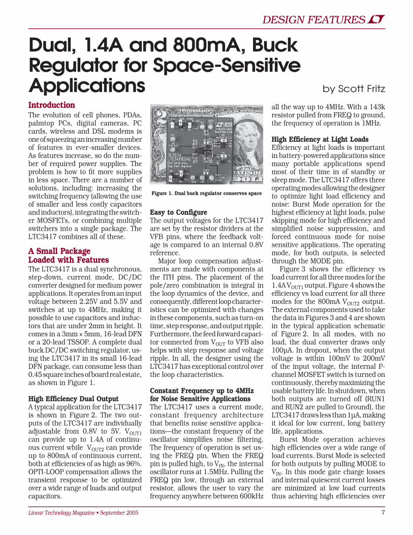
A Small Package Loaded with FeaturesThe LTC3417 is a dual synchronous, step-down, current mode, DC/DC converter designed for medium power applications. It operates from an input voltage between 2.25V and 5.5V and switches at up to 4MHz, making it possible to use capacitors and induc-tors that are under 2mm in height. It comes in a 3mm × 5mm, 16-lead DFN or a 20-lead TSSOP. A complete dual buck DC/DC switching regulator, us-ing the LTC3417 in its small 16-lead DFN package, can consume less than 0.45 square inches of board real estate, as shown in Figure 1.
High Efficiency Dual OutputA typical application for the LTC3417 is shown in Figure 2. The two out-puts of the LTC3417 are individually adjustable from 0.8V to 5V. VOUT1 can provide up to 1.4A of continu-ous current while VOUT2 can provide up to 800mA of continuous current, both at efficiencies of as high as 96%. OPTI-LOOP compensation allows the transient response to be optimized over a wide range of loads and output capacitors.
Easy to ConfigureThe output voltages for the LTC3417 are set by the resistor dividers at the VFB pins, where the feedback volt-age is compared to an internal 0.8V reference.
Major loop compensation adjust-ments are made with components at the ITH pins. The placement of the pole/zero combination is integral in the loop dynamics of the device, and consequently, different loop character-istics can be optimized with changes in these components, such as turn-on time, step response, and output ripple. Furthermore, the feed forward capaci-tor connected from VOUT to VFB also helps with step response and voltage ripple. In all, the designer using the LTC3417 has exceptional control over the loop characteristics.
Constant Frequency up to 4MHz for Noise Sensitive ApplicationsThe LTC3417 uses a current mode, constant frequency architecture that benefits noise sensitive applica-tions—the constant frequency of the oscillator simplifies noise filtering. The frequency of operation is set us-ing the FREQ pin. When the FREQ pin is pulled high, to VIN, the internal oscillator runs at 1.5MHz. Pulling the FREQ pin low, through an external resistor, allows the user to vary the frequency anywhere between 600kHz
all the way up to 4MHz. With a 143k resistor pulled from FREQ to ground, the frequency of operation is 1MHz.
High Efficiency at Light LoadsEfficiency at light loads is important in battery-powered applications since many portable applications spend most of their time in of standby or sleep mode. The LTC3417 offers three operating modes allowing the designer to optimize light load efficiency and noise: Burst Mode operation for the highest efficiency at light loads, pulse skipping mode for high efficiency and simplified noise suppression, and forced continuous mode for noise sensitive applications. The operating mode, for both outputs, is selected through the MODE pin.
Figure 3 shows the efficiency vs load current for all three modes for the 1.4A VOUT1 output. Figure 4 shows the efficiency vs load current for all three modes for the 800mA VOUT2 output. The external components used to take the data in Figures 3 and 4 are shown in the typical application schematic of Figure 2. In all modes, with no load, the dual converter draws only 100µA. In dropout, when the output voltage is within 100mV to 200mV of the input voltage, the internal P-channel MOSFET switch is turned on continuously, thereby maximizing the usable battery life. In shutdown, when both outputs are turned off (RUN1 and RUN2 are pulled to Ground), the LTC3417 draws less than 1µA, making it ideal for low current, long battery life, applications.
Burst Mode operation achieves high efficiencies over a wide range of load currents. Burst Mode is selected for both outputs by pulling MODE to VIN. In this mode gate charge losses and internal quiescent current losses are minimized at low load currents thus achieving high efficiencies over
Dual, 1.4A and 800mA, Buck Regulator for Space-Sensitive Applications
Figure 1. Dual buck regulator conserves space
by Scott Fritz

8 Linear Technology Magazine • September 2005
DESIGN FEATURES
a wide load current range. At low load currents, the control loop turns off all unnecessary circuitry, and stops switching for short periods of time. This generates variable frequency VOUT ripple components that change with load current. Of the three modes, the output voltage ripple is high-est in Burst Mode operation—up to 25mVP–P.
Where supply noise suppression takes on more importance than efficiency, especially in telecommu-nications devices, pulse skipping mode can be selected by pulling the MODE pin to ground. This mode does not have the wide range of high effi-ciency that Burst Mode has, but the voltage ripple is minimized and the frequency components of that ripple
are controlled over a wider load current range. At lower load currents, where the output skips pulses, there can be variable frequency components in the voltage ripple, but the ripple is only around 5mVP–P.
To reduce ripple noise even fur-ther use forced continuous mode. This mode decreases the ripple noise by sustaining the switching of the MOSFETS over all load currents, which results voltage ripple below 5mVP–P, while trading off efficiencies at low load currents. Since the MOSFETS are always switching, the voltage ripple is constant, allowing for better filtering of the voltage ripple noise. Forced continuous mode is selected by setting the MODE pin at VIN/2.
Out of Phase Operation Reduces Ripple and Increases EfficiencyTo help reduce noise on the input voltage, and reduce the size of input capacitor, the two outputs on the LTC3417 can be selected to operate out of phase. The second output, when the PHASE pin is low, operates 180 degrees out of phase with the first channel. Out-of-phase operation produces lower RMS current on VIN and thus lowers RMS derating on the capacitor on VIN.
A High Efficiency 2.25V Dual Step-Down DC/DC Converter with all Ceramic CapacitorsThe low cost and low ESR of ceramic capacitors make them a very attractive choice for use in switching regula-tors. Unfortunately, the ESR is so low that it can cause loop stability problems. Solid tantalum capacitor
MODE
SW1
RUN1
VFB1
PHASE
ITH1
PGOOD
SW2
RUN2
VFB2
FREQ
ITH2
VIN1
LTC3417
GNDAEXPOSED
PAD GNDD
VIN2
CIN10µF
CIN10.1µF
CIN20.1µF
L11.5µH
L22.2µH
C1 22pF
R1 511k
C2 22pF
R3 866k
VIN VIN
VIN
R7100k
R2412k
R4412k
COUT210µF
R55.9k
R62.87k
C32200pF
C46800pF
COUT122µF
VOUT11.8V1.4A
VOUT22.5V800mA
VIN2.25V TO 5.5V
L1: MIDCOM DUS-5121-1R5RCOUT1: KEMET C1210C226K8PAC
L2: MIDCOM DUS-5121-2R2RCOUT2, CIN: KEMET C1206C106K4PAC
Figure 2. Dual output converter produces 1.8V at 1.4A and 2.5V at 800mA, with ceramic input and output capacitors.
LOAD CURRENT (A)
70
EFFI
CIEN
CY (%
)
80
85
95
100
0.001 0.1 1 1060
0.01
90
75
65
VIN = 2.5VVOUT = 1.8V
Burst ModeOPERATIONPULSE SKIPFORCEDCONTINUOUS
Figure 3. 1.4A VOUT1 Efficiency.
LOAD CURRENT (A)
0.001
80
EFFI
CIEN
CY (%
)
90
100
0.01 0.1 1
70
75
85
95
65
60
VIN = 3.6VVOUT = 2.5V
Burst ModeOPERATIONPULSE SKIPFORCEDCONTINUOUS
Figure 4. 800mA VOUT2 Efficiency
VIN = 3.6VVOUT = 1.8VILOAD = 100mA
IL 250mA/DIV
VOUT1 20mV/DIV
2µs/DIV
Figure 5. Burst Mode
VIN = 3.6VVOUT = 1.8VILOAD = 100mA
IL 250mA/DIV
VOUT1 20mV/DIV
2µs/DIV
Figure 6. Pulse Skipping
VIN = 3.6VVOUT = 1.8VILOAD = 100mA
IL 250mA/DIV
VOUT1 20mV/DIV
2µs/DIV
Figure 7. Forced Continuous
continued on page 27
Linear Technology Magazine • September 2005 9
DESIGN FEATURES
IntroductionThe LTC6078 and LTC6079 are dual and quad micropower, precision op amps that combine the low offset and drift of traditional bipolar amplifiers with the low bias current of CMOS amplifiers. Additionally, the LTC6078 features low supply current and low noise, low supply voltage operation, and rail-to-rail input and output stages. This combination of features allows precision performance previ-ously available only through composite amplifiers, manual offset trimming, or calibration.
A Superior Op AmpTraditional bipolar op amps can be designed for excellent precision over temperature, but bipolar amplifiers lack the low bias currents of CMOS amplifiers. In high source impedance applications, a few nanoamps of input bias current can equal millivolts or more of input error, swamping the amplifier’s low VOS.
Traditional (and some non-tradi-tional) CMOS amplifiers come with their own set of strengths and weak-nesses. Input bias current can be much lower than their bipolar counterparts. But VOS and VOS drift specifications often limit the usefulness of these am-plifiers in high-precision applications,
presenting the opposite problem of bipolar amplifiers. Chopper-stabilized (also known as zero drift) amplifiers, which are generally CMOS based, em-ploy a synchronous offset cancellation scheme to negate the DC imperfec-tions of the amplifier, so that VOS and VOS drift of the amplifier become almost negligible. However, zero drift
amplifiers tend to draw much more current than their continuous-time counterparts, precluding their use in low-power precision applications. Additionally, zero drift amplifiers may be much noisier at higher frequen-cies due to auto-zero circuit clock harmonics.
The LTC6078 is a CMOS op amp with a proprietary VOS trimming circuit that yields 25µV maximum VOS and 0.7µV/°C maximum VOS drift, lowest among all comparable bipolar and CMOS op amps. Combined with the 50pA maximum input bias current
over the entire temperature range, the LTC6078 is ideal for all precision or high-impedance instrumentation applications. The low 54µA supply cur-rent and 2.7V minimum supply voltage make the LTC6078 an excellent choice for power-sensitive or hermetically sealed circuits. An LTC6078 dual op amp circuit with passive high-imped-ance sensors can run on two alkaline AA batteries for over 1.5 years.
Precision Current Sense and ControlThe LTC6078’s rail-to-rail input and output stages allow precision input sensing right at VDD or VSS, which is useful for simple high-side or low-side current sensing. Figure 1 shows the LTC6078 in a simple, precise high-side current sensing application. The 25µV precision translates to excellent cur-rent resolution with a very small sense resistor, meaning more precision with less power loss. Used in a feedback loop, the LTC6078 can be used as a precision current source/sink or as a current servo.
Figure 2 shows the LTC6078 bal-ancing the loads on two paralleled LT1763 low dropout (LDO) voltage regulators. A common practice when paralleling two voltage regulators is to simply tie the two outputs together. However, internal voltage offsets cause one regulator to handle the bulk (or all) of the load current. In the case of sink-source regulators, one may be sourcing a great deal of current into the other regulator!
Load sharing circuits work best when the contribution to output current is balanced between the regulators. The LTC6078 compares the voltage outputs of the two LDOs and servos the feedback pin of the second to balance them. The high
µPower Precision Dual Op Amp Combines the Advantages of Bipolar and CMOS Amplifiers
by Cheng-Wei Pei and Hengsheng Liu
–
+
LOADIBIAS
R1100Ω
VDD
2N7002
VDD
RSENSE1Ω
R21k0V < VOUT < VDD – VGS(MOSFET)
IL
I1
VOUT = • RSENSE • I1
R2R1
Figure 1. Precision, low-supply-voltage current sense amplifier. The LTC6078 servos the N-channel MOSFET drain current so that the voltage across R1 is the same as the voltage across the sense resistor. The precision of the LTC6078 enables a small sense resistor to be used for less power dissipation without sacrificing DC accuracy.
An LTC6078 circuit with passive high-impedance sensors can run on two
alkaline AA batteries for over 1.5 years.

10 Linear Technology Magazine • September 2005
DESIGN FEATURES
precision of the LTC6078 means that discrete ballast resistors are unneces-sary—short pieces of wire or PCB trace are sufficient to provide the ballast resistance. With 25mΩ of resistance1, the LTC6078 can balance the current sharing of the LDOs to be within 1mA, regardless of the absolute load cur-rent output. The feedback network does not noticeably degrade the load transient performance of the regula-tors, and Figure 2 can be expanded to include as many paralleled regulators as necessary.
Shutdown FunctionFor extremely low power applications such as hermetically sealed battery-powered sensors, the 10-pin version of the LTC6078 in the tiny DFN package offers two shutdown pins (one for each amplifier). When in shutdown mode, the low 54µA per amplifier current draw is reduced to a maximum of 1µA (over the entire temperature range). The fast 50µs turn-on and 2µs turn-off times ensure that minimal power is dissipated during the transition periods.
In applications where many inputs need to be monitored and only a single analog-to-digital converter is available, the independent shutdown function of the two amplifiers allows any number of LTC6078 outputs to be multiplexed together. The high-impedance output of the LTC6078 in shutdown mode does not load the output of an active LTC6078. So long as two amplifiers are not simultaneously active, there
is no need for external multiplexing components.
Layout ConsiderationsIn high source impedance applications such as pH probes, photodiodes, strain gauges, et cetera, the LTC6078’s low input bias current (50pA maximum over temperature) requires a clean board layout to minimize additional leakage current into a high-imped-ance signal node. A mere 100GΩ of PC board resistance between a 5V supply trace and an input trace adds 50pA of leakage current, which is typically greater than the input bias current of the LTC6078. For compari-son, a bit of unwashed soldering flux
can add a 1GΩ–10GΩ resistance. In critical applications, or if leakage is suspected, a guard ring around the high-impedance input traces driven by a low-impedance source to equal the input voltage prevents such leak-age problems. The guard ring should extend as far as necessary to shield the high-impedance signal from any and all potential leakage paths. Figure 3 shows the recommended layout when using a guard ring.
ConclusionThe LTC6078 offers all of the benefits of both bipolar and CMOS amplifiers, as well as a slew of other features that make it the ultimate choice for low power, precision applications. The combination of excellent offset, drift, and input bias current specifications is unmatched among both bipolar and CMOS op amp offerings. For applications requiring four precision op amps, the LTC6079 is available in 16-pin surface-mount SSOP and DFN packages. Notes1 A 25mΩ resistor is equal to approximately 5 inches
of AWG 28 gauge copper stranded wire or 1.25 inches of a 25 mil wide one-ounce copper PCB trace at room temperature.
LTC6078 CMS8
R
OUT
IN–
IN+
V–
LEAKAGECURRENT
NO LEAKAGECURRENT
GUARDRING
6
5
4
4
NO SOLDER MASKOVER THE GUARD RING
Figure 3. A sample layout using a low-impedance guard ring to shield a high-impedance signal trace from board leakage sources. The output pin can drive the guard ring directly or through a low impedance (<100kΩ) feedback resistor. The amplifier is shown in a non-inverting gain configuration.
IN
SHDN
GND
OUT
BYP
FB
0.01µF
0.01µF
10µF
10µF
IN
SHDN
GND
OUT
BYP
FB
0.01µF 10µF
R12k
R12k
R22k
R22k
100Ω
10k
1k
–
+
LOADIL
LTC6078
VIN1.8V TO
20V LT1763
LT1763
0A ≤ IOUT ≤ 1ALOAD MATCHING TO WITHIN 1mA WITH 25mΩ OF TRACE LENGTH (5 INCHES OF 28-GAGE STRANDED WIRE)1.22V ≤ VOUT ≤ VDD (OF LTC6078)
IDENTICAL LENGTH,THERMALLY MATEDWIRE OR PCB TRACE
VOUT = 1.22V (1 + )R1R2
Figure 2. The LTC6078 used as a current load balancing servo amplifier. Short lengths of copper wire or PCB trace can be used as ballast resistors due to the LTC6078’s precision. VDD of the LTC6078 may be connected to VIN or VOUT , as long as the minimum 2.7V supply voltage requirement is met.
Authors can be contactedat (408) 432-1900

Linear Technology Magazine • September 2005 11
DESIGN FEATURES
IntroductionSome of the harshest environments for electronic circuits are found in industrial and automotive applica-tions, where high, unpredictable input voltage transients, failing batteries and disconnected supplies are an expected part of doing business. A 12V car bat-tery and a 48V industrial supply rail offer many of the same power supply design challenges. Input voltages can spike to 75V on an industrial rail or 60V during an automotive load dump. Cold cranking or overloaded lines can drop the supply voltage to only a few volts. Through all of this, the power supply must be kept alive and remain in regulation for critical circuitry, and it cannot dissipate much quiescent power—dead car batteries or lost in-dustrial sensor data do not make for happy customers.
Tough New Regulators Provide Flexibility in Rough EnvironmentsThree new linear regulators provide flexible options when running in these environments. The LT3012 and LT3013 provide up to 250mA at a dropout voltage of 360mV, and the LT3014 provides up to 20mA at a dropout voltage of 350mV.
The LT3012 and LT3013 offer an input voltage range of 4V to 80V and minimize power loss by running with quiescent currents of 55µA (LT3012) and 65µA (LT3013). Quiescent current is reduced to just 1µA in shutdown.
Both are stable with only a small 3.3µF capacitor on the output. Small ceramic capacitors can be used with-out any need for additional series resistance as is common with other regulators. The LT3013 adds a power good flag, PWRGD, to indicate that the output is above 90% of nominal, with a delay that is programmable using a single capacitor. Both the LT3012 and LT3013 are offered with adjustable outputs and a 1.24V reference voltage. The regulators are packaged in the 16-lead TSSOP and 12 pin low profile (0.75mm, 4mm × 3mm) DFN pack-ages with exposed pads for enhanced thermal handling capability. These
High Voltage Micropower Regulators Thrive in Harsh Environments
surface mount packages are capable of handling 1W to 3W of continuous dissipation and much higher peak transients. See the data sheet for a detailed discussion.
The LT3014 offers a 3V to 80V input voltage range, and the 7µA operating quiescent current (1µA in shutdown) makes it an attractive choice for power-critical systems. The LT3014HV is a higher voltage option of the regulator that is rated to withstand 100V tran-sients for up to 2ms. The regulator is stable with only 0.47µF of capacitance on the output—small ceramic capaci-tors can be used without any need for added series resistance. It is available as an adjustable part with a 1.22V reference voltage and is packaged in the 5-lead ThinSOT and 8-lead (3mm × 3mm) DFN packages.
All of the regulators have internal protection circuitry for reverse-bat-
Table 1. Linear Technology High Voltage Linear Regulator Portfolio
Part # Output Current
Maximum Input Voltage
Dropout Voltage
Quiescent Current
Output Capacitor Added Features
LT3014 20mA 80V 350mV 7µA 0.47µF 5-lead ThinSOT Package or 8-lead (3mm × 3mm) DFN
LT3014HV 20mA 100V (2ms Survival) 350mV 7µA 0.47µF 5-lead ThinSOT Package or
8-lead (3mm × 3mm) DFN
LT3010 50mA 80V 300mV 30µA 1µF 8-lead Thermally Enhanced MSOP Package
LT3012 250mA 80V 360mV 55µA 3.3µF 16-lead TSSOP or 12-lead (4mm × 3mm) DFN Thermally Enhanced Packages
LT3013 250mA 80V 360mV 65µA 3.3µF All Features of the LT3012 Plus a PWRGD Flag with Programmable Delay
by Todd Owen
IN
LT3014
SHDN1µF
VIN3.7V TO80V
OUT
ADJGND
VOUT3.3V20mA
0.47µF2.05M
1.21M
VSHDN<0.3V>2.0V
NC
OUTPUTOFFONON
Figure 1. LT3014 3.3V/20mA keep-alive supply with shutdown

12 Linear Technology Magazine • September 2005
DESIGN FEATURES
a maximum input voltage of 80V. If a higher output current is needed, the LT3012 and LT3013 are now available. Figure 2 shows a 5V supply that can provide up to 250mA of current using the LT3013. This supply operates at only 65µA quiescent current and re-quires only 3.3µF of capacitance on the output. An added feature that this part has is a PWRGD flag that indicates when the ADJ pin is within 10% of its nominal voltage of 1.24V.
The PWRGD flag of the LT3013 can be used to provide a micropro-cessor reset signal or other logic flag. Figure 3 shows the block diagram for the PWRGD flag. The PWRGD pin is an open-collector output, capable of sinking 50µA when the output is low; there is no internal pull-up on the PWRGD pin, an external resistor must be used. When the output rises to within 10% of its final value, a JK flip-flop allows a 3µA current source to begin charging the capacitor on the CT pin. As the CT pin reaches its trip level (approximately 1.6V at 25°C), the 3µA current is shunted away to clamp the capacitor voltage and set the PWRGD flag state to high impedance.
During normal operation, an inter-nal glitch filter ignores short transients (<15µs) on the output voltage. Longer
tery, current limit, thermal limit, and reverse voltages from output to input. Table 1 provides a summary feature comparison of these and other high voltage linear regulators.
High Voltage Low Current Keep-Alive Regulator ApplicationFigure 1 shows a typical applica-tion using the low current LT3014 to provide a 3.3V keep-alive supply, such as a real-time clock, a security system, or any other system that runs constantly from a battery. The 7µA quiescent current keeps the power supply from being a significant drain on the battery.
The resistor divider is sized to match the tiny operating currents of the LT3014. Care must be exercised when operating at such low currents, since a small error can cause large percentage shifts. Insufficient clean-ing of solder flux after assembly can provide resistances in the MΩ range, leading to erroneous outputs.
The SHDN pin of the LT3014 can be driven to GND by external circuitry to turn the output of the regulator off and reduce operating current. Leaving the SHDN pin open or pulling it above 2V will turn the regulator on.
The output of the LT3014 needs only the 0.47µF capacitor for stability. The regulator is designed to be stable with the widest possible range of output capacitors—the ESR of the output capacitor can be zero, as is common with small ceramic capacitors, or can be as high as 3Ω, a value found more often with small tantalum or aluminum electrolytic capacitors. The minimum output capacitor coupled with the micropower nature of the LT3014 tends to give larger voltage deviations with fast transients, so larger values are recommended if there are large current steps.
Higher Output Current Supply with PWRGD FlagWhen higher output currents are needed, Linear Technology offers several options. The LT3010 regulator can provide 50mA of output current at a maximum dropout of 300mV and
transients below the 10% low threshold will reset the internal JK flip-flop. This flip-flop ensures that the capacitor on the CT pin is fully discharged to the VCT(LOW) threshold before re-starting the time delay. This is done to provide a consistent time delay after the output returns to within 10% of its regulated voltage before the PWRGD pin switches to the high impedance state.
If the PWRGD function of the LT3013 is not needed for your applica-tion, the LT3012 can be used to provide the same regulator performance. The removal of the PWRGD circuitry allows the LT3012 to operate at a lowered quiescent current of 55µA.
ConclusionThree new regulators satisfy the needs of tough automotive and industrial electrical environments. A range of possible output currents and qui-escent currents allow designers to pick a solution that can limit power dissipation during normal operation while still providing the capability to handle high voltage transients. The most important feature of these devices is that they can withstand the rigors of the worst electrical environments, thus ensuring a steady power supply for critical circuits.
–
+
–
+
VREF • 90%
VCT(LOW)≈0.1V
VCT(HIGH) – VBE≈1.1V
ICT3µA
ADJ
J Q
K
PWRGDCT
Figure 3. PWRGD circuit block diagram
IN
LT3013
SHDNCIN
2.2µF
CDELAY22nF
CT
5.4V TO80V OUT
PWRGD PWRGD
ADJ
GND
5V250mA
COUT3.3µF
RPWRGD100k
R1750k
R2249k
Figure 2. LT3013 5V/250mA supply provides PWRGD flag

Linear Technology Magazine • September 2005 13
DESIGN FEATURES
IntroductionOne of the most popular battery solu-tions for consumer handheld devices is the venerable two-cell AA (alkaline or nickel-metal hydride) source, especially in GPS navigators, digital cameras and MP3 players. AA bat-teries are readily available, relatively low cost and offer high power density. Many of these same portable devices supplement battery power with plug-in wall adapter and offer a USB bus (for data transfer). The USB bus can also be used to provide power. The problem is how to seamlessly switch between these three disparate types of supplies: 2-cell AA, wall and USB. The solution is the LTC3456.
The LTC3456 is a complete system power IC that seamlessly manages power flow between an AC wall adapter, USB and 2-AA battery, while comply-ing with USB power standards—all in a 4mm × 4mm QFN package (Figure1). The device generates two separate power rails: a 3.3V (fixed) main supply and a 1.8V (adjust-able) core supply. In addition, the
Complete 2-Cell-AA/USB Power Manager in a 4mm × 4mm QFN
LTC3456 contains a fully featured USB power manager, a Hot Swap output for powering memory cards and an un-
committed gain block suitable for use as a low-battery comparator or an LDO controller. The device also generates an always-alive VMAX output, suitable
for supplying power to critical blocks like the real time clock, which needs to stay alive even during shutdown.
About the LTC3456The LTC3456 contains four high efficiency 1MHz fixed frequency switching regulators that operate with efficiencies up to 92%. Figure 2 shows a typical LTC3456 application. Most processors used in portable ap-plications require dual power supply voltages. These voltages can be 3.3V for the I/O circuitry and 1.5V or, 1.8V for the processor core. Additionally, the processor might require that the power supplies startup in a specific sequence to prevent processor latch
by G. Thandi
+
WALLFB
PWRKEYVMAX
VEXT
10µF
MBRM120E
4.7µF
4.7µF
1k
11.3k
ON/OFF
1Ω
1Ω
4.7µF
AC WALLADAPTER
(5V ±10%)
USB POWER(4.35V TO 5.5V)
USBCONTROLLER
4.32k
80.6k
100k
L24.7µH
2 AACELLS L3
10µH
EXT_PWR
USB
SUSPEND
USBHP
AO
AIN VMAIN
VBATT VINTSW2_BST
LTC3456
SW2_BK
PBSTAT RESET MODE
µP
PWRON PGND AGND
22µF
VINT3.3V
MAIN OUTPUT3.3V150mA1µF
HSOHot Swap OUTPUT3.3V50mA1µF
1µF
SW1
FB1
L110µH CORE OUTPUT
1.8V200mA
VMAX(POWERSREAL-TIME CLOCK)
10µF
220pF100k
80.6k
Figure 2. A LTC3456-based, complete power solution, including a 1.8V output for processor core, a 3.3V output for the I/O, a 3.3V Hot Swap supply for the memory card and a VMAX output for RTC. This design uses all ceramic capacitors with minimal parts count.
USB POWER
AC ADAPTER
2 AA CELLS
DSP CORE
MEMORY CARD
DSP I/O
VCORE (1.8VADJ)
VMAIN (3.3V)
VMAX
HOT SWAP (3.3V)
REAL-TIME CLOCK
LTC3456
• SMART SELECTION OF POWER SOURCE
• USB POWER MANAGER
• HIGH EFFICIENCY DC/DC CONVERTERS
Figure 1. The LTC3456 is a complete system power management IC available in a tiny 4mm×4mm package.
The LTC3456 squeezes a USB power manager, four high
efficiency DC-DC converters, a Hot Swap controller, a low-battery indicator and much more into a
4mm × 4mm QFN package.

14 Linear Technology Magazine • September 2005
DESIGN FEATURES
up or improper initiation. Usually the core supply must come up before the I/O supply.
The LTC3456 has in built power supply sequencing for the core and main outputs. At power-up, the VINT output, a fixed 3.3V supply, is the first one to power up. It supplies power to most of the internal circuitry. The amount of external loading at this output should be limited (Refer to the LTC3456 datasheet for more details). The core output, adjustable from 0.8V to 1.8V, comes up next followed by the VMAIN output. The VMAIN output, a fixed 3.3V supply, powers up with a delay of 0.8ms (typ) after the core output comes into regulation. The VMAIN out-put is generated from the VINT output through an internal 0.4Ω (typ) PMOS switch and can be used to power the I/O circuitry. The 0.8ms delay gives sufficient time to the processor to stabilize the system clock and load internal registers before the peripheral circuitry powers up.
The LTC3456 produces a Core output, adjustable from 0.8V to 1.8V suitable for powering new low voltage processors (ARM and others). The LTC3456 control scheme allows 100% duty cycle operation for the core out-put. It provides low dropout operation when the core output is powered from the battery, thereby extending battery life. Both Main and Core converters offer Burst Mode operation (MODE Pin selectable) when powered from the battery resulting in high efficiency at light loads as seen in Figure 3. The Core converter features greater
than 92% efficiency when powered from the battery. Burst Mode opera-tion is disabled when powered from USB/wall power. Figure 4 shows the system efficiency when powered from the USB. The Main converter achieves up to 90% efficiency when powered from the USB.
The LTC3456 has a built-in Hot Swap output suitable for powering flash memory cards. The Hot Swap out-put features short-circuit and reverse voltage blocking capability. It allows memory cards to be hot swapped into and out of the system. It has a built-in 120mA(typ) current limit suitable for powering flash memory cards.
The LTC3456 features short-cir-cuit protection for both the main and core outputs. It also provides output disconnect for all the outputs with the exception of the VMAX output. The Core, Main and Hot swap outputs are
all discharged to ground in shutdown. The VMAX output is the highest of the VBATT, VINT,VEXT and USB voltages. This output can be used to supply a maximum of 1mA output current. The VMAX output stays alive even when the IC is in shutdown and is suitable for supplying power to critical system blocks like a real time clock.
PowerPath ControlThe LTC3456 contains a proprietary PowerPath control scheme that seam-lessly switches over the system power from a 2-AA battery to USB/wall Power and vice versa. Figure 5 shows a sim-plified block diagram of the internal power-path. The AC adapter and the USB bus supply power to the switch-ing regulators via the VEXT pin. The LTC3456 contains a full featured USB power manager to control the flow of power from the USB pin via the state of the USBHP and SUSPEND pins. The current through the USB pin is accurately limited to 100mA or, 500mA depending on the state of the USBHP pin. All USB functionality can be disabled by pulling the SUSPEND pin high.
DC-DC conversion is a particularly challenging task when the 2 AA bat-tery voltage (1.8V to 3.2V) must be boosted to generate 3.3V output, and the USB/wall power (4V to 5.5V) must be stepped down to generate the same voltage. The LTC3456 accomplishes this task via the BOOST and BUCK2 converters. This is the most efficient
USBMANAGER
USBUSBPOWER
SW1
VBATT SW2_BST
VINT
VINT3.3V
VEXT
SW2_BK
BUCK 1 BUCK 2
BUCK 3 BOOST
CORE1.8V 10µF
4.7µF
4.7µF2AA CELL
10µF
10µH10µH
4.7µH
LTC3456
10µF
AC ADAPTER5V ±5%
Figure 5. LTC3456’s simplified block diagram showing internal PowerPath.
LOAD CURRENT (mA)1
60
EFFI
CIEN
CY (%
)
80
100
10 100 1000
40
30
50
70
90
20
0
10 VBATT = 2.4VVCORE = 1.8V
PWM MODEBurst ModeOPERATION
Figure 3. Core converter efficiency for Figure 2’s circuit. LTC3456 is powered from the battery. Efficiency is shown for both PWM and Burst Mode operation.
LOAD CURRENT (mA)1
60
EFFI
CIEN
CY (%
)
80
100
10 100 1000
40
30
50
70
90
20
0
10
VUSB = 5VVUSBHP = 2V
1.8V OUTPUT3.3V OUTPUT
Figure 4. Core and Main converter efficiency for Figure 2’s circuit. The LTC3456 is powered from the USB with the USB current limit set at 500mA (USBHP = High).

Linear Technology Magazine • September 2005 15
DESIGN FEATURES
way of generating the 3.3V power rail. The LTC3456 achieves efficiency greater than 90% when generating 3.3V output from the battery or USB/wall adapter. The core output (1.8V) is generated via BUCK1 (USB/wall Pow-ered) and BUCK3 (Battery Powered) converters. The unique topology of LTC3456 generates the 1.8V rail via a single inductor resulting in a cost and space saving. It achieves efficiency greater than 92% when generating the 1.8V output from the battery. The various operational modes of LTC3456 are summarized in Table 1.
Portable devices are required to seamlessly switch-over from the battery power to USB or wall power and vice versa to ensure smooth system operation. As an example, a user is playing music on a portable MP3 player with the USB cable con-nected. If the USB cable is suddenly yanked off the device, the user should be able to continue listening to the music without any interruption. The LTC3456 makes it possible through seamless switchover of system power.
Figure 6 shows USB and 2-AA battery power supply switchover waveforms for Figure 2’s circuit. The USB power is unavailable when the Suspend pin is taken from low to high. Main and core outputs both exhibit less than ±2% total deviation at the time of switchover making the switchover seamless to the processor core and the peripheral circuitry.
Easy Interfacing with a MicroprocessorThe LTC3456 simplifies the task of interfacing with a micro-processor. The PWRON, PWRKEY, PBSTAT and RESET pins provide all the required system information to the processor and simplify power sequencing. The PWRON, PWRKEY and PBSTAT keys simplify the task of orderly powering-up and shutting down the IC. The datasheet contains the timing diagram and gives detailed information about their operation.
The LTC3456 also contains power-on reset circuitry (accessed via pin RESET) that is active during both
power-up and shutdown. The pow-er-on reset is required to hold the processor in its reset state at power-up and it must keep the processor from starting operation until all system power supplies have stabilized. The LTC3456’s built in power-on reset circuitry monitors both the VINT (3.3V) and Core (1.8V) voltages and interfaces to the processor via the RESET pin. The RESET pin is held low during initial power-up. When both the Main and Core outputs come into regulation, a reset delay timer gets activated. There is a full 262ms timeout before RESET is released and the processor is allowed to come out of reset and begin opera-tion. The timeout delay of 262ms gives sufficient time for the processor to initialize the internal registers/RAMs. During power-off the RESET pin is again pulled low. This prevents the micro-processor from entering into any random operational modes.
Figure 7 shows the power-up and power down waveforms for the circuit of Figure 2 in battery powered mode. The RESET circuitry works similarly
Table 1. Summary of LTC3456 PowerPath operational modes and features
AC ADAPTER USB POWER 2 AA CELLS
Highest priority for powering the IC Medium priority for powering the IC Lowest priority for powering the IC
Battery loading < 2µA Battery loading < 2µA Burst Mode operation (User Selectable) conserves battery energy
Internal soft-start circuitry limits current drawn from the adapter at start-up
USB pin current accurately limited to 100mA or 500mA
Battery inrush current regulated during power-up. Additionally, internal soft-start limits input current at start-up.
AC adapter (min) voltage set via the WALLFB Pin USB (min) voltage set to 4V Battery (min) voltage indicator set via the AIN Pin
VCORE100mV/DIV
(AC COUPLED)
IL1100mA/DIV
SUSPEND5V/DIV
200µs/DIVVUSB = 5VVUSBHP = 5VVBATT = 2.4VICORE = 100mAIMAIN = 100mA
VMAIN100mV/DIV
(AC COUPLED)IL2
200mA/DIV
IL3100mA/DIV
SUSPEND5V/DIV
200µs/DIVVUSB = 5VVUSBHP = 5VVBATT = 2.4VICORE = 100mAIMAIN = 100mA
Figure 6. USB and 2AA Battery power supply switchover waveforms for Figure 2’s circuit. The USB power is disconnected when the Suspend pin is taken high. Main and core outputs both exhibit less than ±2% total deviation at the time of switchover.
a. Core output transient waveforms b. Main output transient waveforms
VPWRON5V/DIVVMAIN
5V/DIV
VCORE2V/DIV
RESET5V/DIV
100ms/DIVVBATT = 2.4VICORE = 10mAIMAIN = 10mA
Figure 7. Power-up and power-down waveforms for Figure 2’s circuit. Both VMAIN and VCORE outputs are discharged to ground during shutdown. Power-on reset ( RESET) is held low for a delay of 262ms after VCORE comes into regulation.

16 Linear Technology Magazine • September 2005
DESIGN FEATURES
when battery or externally powered. The RESET pin is held low for a de-lay of 262ms after VCORE comes into regulation. When the IC is shut-down, both VMAIN and VCORE outputs are dis-connected from the input power and discharged to ground This prevents the outputs from being stuck in an indeterminate logic-level state and adversely affecting the operation of the microprocessor. It also ensures that the outputs rise in a predictable fashion during power-up.
Voltage MonitoringThe LTC3456 has an on-chip gain block that can be used for low-battery detection, with the low battery trip point set by two resistors (Figure 2) at the AIN pin. The nominal voltage at AIN is 0.8V. The AO pin is an open-drain logic output that sinks current whenever the voltage at the pin AIN falls below 0.8V. The gain block can also be configured to drive an external PNP or PMOS transistor to generate an auxiliary voltage.
In addition, the LTC3456 has on board voltage comparator circuitry to detect the presence of USB or wall power, with a status output at the EXT_PWR pin. The open-drain logic output of EXT_PWR is capable of sinking up to 5mA, suitable for driving an external LED. The on-board voltage detectors continuously moni-tor the status of the USB voltage and AC adapter voltage (via the WALLFB Pin). Whenever the USB or, wall power is available and in regulation, the EXT_PWR pin is pulled low.
Portable GPS Navigator Power SupplyToday’s portable GPS navigators run off two AA batteries or an AC adapter and come equipped with a USB bus (for data transfer). Long battery life and small system size are the key requirements for the power supply. The microprocessor used in GPS navigators usually require at least two different voltage supplies: typically 3.3V for the I/O circuitry and 1.5V or
1.8V for the processor core. The navi-gator might also require an auxiliary 2.8V supply voltage to bias the LCD display controller IC.
Figure 8 shows a complete, com-pact and efficient power supply for a portable GPS navigator. The VMAIN (fixed 3.3V) provides power to the I/O circuitry. The power supply for the processor core, VCORE, is set at 1.8V and can be adjusted by changing the feedback resistor ratio. The 3.3V Hot Swap output powers flash memory cards. The LTC3456 contains an un-committed gain block (Pins AIN and AO) that can be used as a low-battery indicator or an LDO controller. The circuit in Figure 8 shows the gain block being used as an LDO with an external PNP to generate an auxiliary 2.8V output voltage from the Main output. The auxiliary 2.8V supply is being used to power an LCD controller IC. The VMAX output of the LTC3456 stays alive even in shutdown and is used to supply power to a real-time clock.
+
PWRKEY
WALLFB
VMAX
VEXTVEXTC410µF
C24.7µF
1Ω
C34.7µF
C14.7µF
1k
D1
1Ω
11.3k
4.32k
ACADAPTER
(5V ±10%)
USB POWER(4.35V TO 5.5V)
USBCONTROLLER
L24.7µH
2 AACELLS L3
10µH
EXT_PWR
USB
SUSPEND
USBHP
VBATT VMAIN
A0
AIN
VINTSW2_BST
LTC3456
SW2_BK
PBSTAT RESET MODE
MICROCONTROLLER
PWRON PGND AGND
C1022µF
MAIN OUTPUT3.3V100mA
LCD LOGIC BIAS2.8V10mA
C91µF
100k
HSOFLASH MEMORY CARD3.3V50mAC7
1µF
C82.2µF
Q1
49.9k
20k
C51µF
C1, C6 TO C10: X5R OR X7R, 4VC2 TO C5: X5R OR X7R, 6.3VD1: ON SEMICONDUCTOR MBRM120E
SW1
FB1
L110µH CORE OUTPUT
1.8V200mA
VMAX(TO REAL-TIME CLOCK)
C610µF220pF100k
80.6k
L1, L3: MURATA LQH32CN100K53L2: MURATA LQH32CN4R7M53Q1: PHILIPS MMBT3906
Figure 8. A 2-AA-cell-powered, complete power supply for GPS navigation system. Note that the uncommitted gain block (Pins AIN and AO) is configured as an LDO controller to generate an auxiliary 2.8V output.
continued on page 19

Linear Technology Magazine • September 2005 17
DESIGN FEATURES
IntroductionTraditionally, electronic clocks use quartz crystals, ceramic resonators, or discrete R, L or C elements as a timing reference, but each of these designs has several drawbacks that make them unsuitable for a variety of applications. Quartz crystals and ceramic resonators can be power-hun-gry, and their accuracy is subject to environmental stress. Crystal oscilla-tors have the additional disadvantage of being susceptible to damage from shock or vibration. RC oscillators have poor jitter and accuracy, or require expensive precision components. A more robust, and compact alternative to all of these is an all silicon clock, such as the LTC6906 micropower, resistor-controlled oscillator.
The LTC6906 is a monolithic silicon oscillator with significant size, power, cost and environmental sensitivity advantages over other oscillators, and it requires only a single external resistor to set the frequency over its full range of 10kHz to 1MHz (Figure 1). Its 0.65% accuracy and jitter as low as 0.03% make it an excellent choice for precision applications, and the power and size advantages let the LTC6906 fit in designs where a crystal oscillator could never go.
Device DescriptionThe LTC6906 is a part of Linear Technology’s line of resistor controlled SOT-23 oscillators. These resistor controlled oscillators use a single inexpensive external resistor to ac-curately set the oscillator frequency, and there is a simple linear relation-ship between the resistor value and the output frequency.
The LTC6906 uses an innovative low power architecture with a master oscillator running between 100kHz and 1MHz. A three state, divide pin is provided which can engage an in-ternal divider to decrease the output frequency by a factor of 1, 3 or 10
Micropower Precision Oscillator Draws Only 60µA at 1MHz
to provide a total frequency range of 10kHz to 1MHz. For increased accu-racy at the lower end of the frequency range with very low bias currents, a guard pin is provided for the frequency setting resistor input.
The master oscillator frequency is set by an external resistor connected between the SET pin and ground. The LTC6906 maintains the SET pin at approximately 650mV above ground, with a tempco of –2.2mV/°C. The master oscillator frequency is related to the SET resistor by:
f MHz kRMASTER
SET= •
1 100 Ω ,
and is related only to the resistance on the SET pin, without regard to the exact SET pin current or voltage.
Low Power DissipationThe LTC6906 uses only 10µA when running at 100kHz (Figure 2). There are three components to this current draw. A static bias current of about 5µA is used by the internal reference and bias circuits. A variable bias current of about 6 times the current in the SET resistor is used to power and bias the internal oscillator. A load current related to the load capaci-tance, power supply voltage and load resistance makes up the remainder of the dissipation equation. An approxi-
mate expression for the total supply current is:I A I
V F C pF V
SUPPLY SET
OUT LOAD
= + • +
• • + +•
++
5 6
52
µ
( )RRLOAD
.
Figure 3 shows the relative mag-nitudes of these three components over the frequency range in the case of a load capacitance of 5pF, with no resistive load.
Note that power dissipated in the load ranges from 25% to over 40% of the total power from 100kHz to 1MHz operation. Any lessening in the load capacitance or resistance can have dramatic effects on the load current portion of the power supply dissipa-tion. Power dissipation as low at 7µA at 100kHz is achievable with light output loading. Decreasing the power supply voltage also reduces the power dissipated into the load.
by Albert Huntington
CONT
RIBU
TION
TO
POW
ER D
ISSI
PATI
ON (%
)
SET RESISTOR (kΩ)12000
60
0200 400 600 800 1000
10
20
40
30
50
V+ = 3VTA = 25°C
LOAD CURRENT
SET CURRENT
STATIC BIAS
Figure 3. Percentage contributions to power dissipation of static bias, set current and load currents. Data was taken at 3V, 25ºC ambient temperature.
FREQUENCY (kHz)0
0
POW
ER S
UPPL
Y CU
RREN
T (µ
A)
10
30
40
50
800
90
20
400200 1000600 1200
60
70
80
V+ = 3.6V
V+ = 2.25V
CL = 5pFTA = 25°C
Figure 2. The LTC6906 has extremely low power dissipation.
10kHz TO 1MHz
NO DECOUPLINGCAPACITOR
NEEDED
RSET100k TO 1M
2.25V TO 3.6V
÷1÷3
÷10
V+
GND
DIV
OUT
GRD
SET
LTC6906
Figure 1. The LTC6906 requires only a single external resistor.

18 Linear Technology Magazine • September 2005
DESIGN FEATURES
Engaging the internal divider has larger effects on power dissipation where the load current is higher at higher frequencies, but little effect where the internal bias currents dominate at lower master oscillator fre-quencies, as illustrated in Figure 4.
Choosing a SET ResistorThe choice of a SET resistor is guided by the desired frequency output. The part is specified for master oscillator frequencies between 100kHz and 1MHz, with possible DIV ratios of 1, 3 and 10. These DIV ranges overlap, and some frequencies have multiple valid combinations of DIV and SET resistor values. The lowest power dis-sipation for a given frequency is always obtained by setting the SET resistor as high as possible and DIV as low as possible. Generating 100kHz using DIV = 10 and RSET = 100kΩ dissipates much more power than using DIV = 1 and RSET = 1000kΩ.
The following equation relates the desired master oscillator frequency to the RSET value:
RMN
kHzFSETOUT
= •1 100Ω ;
where N is the divider ratio chosen of 1,3 or 10, RSET is the SET resistor value and fOUT is the desired output frequency. For example, see Table 1 for valid RSET values to generate a 100kHz output frequency at the three DIV settings. It is apparent from the table that, depending on the DIV pin setting, the current for a particular output frequency could vary by a fac-tor of up to 4.5.
There are tradeoffs to choosing the largest possible SET resistor and the smallest possible value of DIV. Jitter increases at the smaller DIV values, and frequency accuracy may suffer
more with high RSET values due to leakage at the SET pin, especially at higher temperatures.
Layout ConsiderationsThe LTC6906 is capable of frequency accuracy of <0.65% over the commer-cial temperature range, and for best accuracy, care must be exercised to limit board leakage around the RSET pin. A 1GΩ parasitic resistance to ground can change the frequency by 0.1%, and the same resistance to the positive supply could increase that to 0.3%. A guard pin which is weakly driven to the same DC voltage as the SET pin has been provided, and the guard signal should be routed completely around the SET pin, on the same side of the PC board as the device, and should have no soldermask (see Figure 5 ).
The guard ring is not be necessary in all applications, especially those with lower values of SET resistor and excel-lent assembly practices. The majority of board leakage problems occur due to insufficient cleaning of flux from the board or from sloppy assembly. With perfectly clean assembly, the guard ring is completely unnecessary.
The LTC6906 uses a switched current to drive the SET resistor, so there may be some noise visible on the SET line. Although this noise does not contribute to jitter on the output signal, it can influence the frequency accuracy in the presence of parasitic capacitance on the SET pin. Because of this sensitivity to parasitic capaci-tance and because of the danger of
additional leakage from long traces, it is recommended that the SET resistor be located as close as possible to the SET pin, and on the same side of the PC board as the LTC6906.
Long Term Drift of Silicon OscillatorsLong-term stability of silicon oscilla-tors is specified in ppm/√kHr, which is typical of other silicon devices such as operational amplifiers and voltage ref-erences. Because drift in silicon-based oscillators is generated primarily by movement of ions in the silicon, most of the drift is accomplished early in the life of the device and the drift can be expected to level off in the long term. The ppm/√kHr unit models this time variant decay. Crystal oscillators are occasionally specified with drift mea-sured in ppm/year. This measurement models a different drift mechanism, and the decay profile is not the same.A comparison of various drift rates over a five year time period is shown in Figure 6.
When calculating the amount of drift to be expected, it is important to consider the entire time in the calcula-tion, because the relationship to time is not linear. The drift for 5 years is not 5 times the drift for one year. A sample calculation for drift over 5 years at 300ppm/√kHr is as follows:5 years • 365.25 days/year • 24 hours/day = 43,830 hours = 43.830kHr
43 830 6 62. .kHr kHr=
6 62 300 0 198 5. • . %kHr ppmkHr
over years=
Table 1. RSET values for 100kHz
Divider Setting N RSET Value
Approximate Supply Current
1 1MΩ 10µA
3 333.33KΩ 20µA
10 100kΩ 45µA
RSET (Ω)0
0
POW
ER S
UPPL
Y CU
RREN
T (µ
A)
10
30
40
50
800
20
400200 1000600 1200
60÷1
÷3
÷10
70
80V+ = 2.7V
Figure 4. The LTC6906 power supply current vs DIV pin setting. All data taken at 3V supply, 5pF load.
Figure 5. The GRD ring should be routed on the same side of the PC board as the LTC6906, and should have the solder mask removed.
LTC6906
RSET
OUT
GND
DIV
LEAKAGECURRENT
NO LEAKAGECURRENT
GUARDRING
V+
GRD
SET
1
2
3
6
5
4
NO SOLDER MASK OVER THE GUARD RING

Linear Technology Magazine • September 2005 19
DESIGN FEATURES
Drift calculations assume that the part is in continuous operation during the entire time period of the calcula-tion. The movements of ions which results in drift is usually aided by electric fields in the operating parts, and drift is substantially lower if the parts are not powered up during the entire period of drift. Conservative calculations would use a tenth of the drift specification for time when power is not applied to the part.
Switching the DIV Pin The DIV input pin on the LTC6906, similar in many ways to the DIV pin on other LTC silicon oscillators, is a three state input, capable of resolv-ing three different states: high, open and low. Three state input pins allow greater functionality in low pin-count packages, and are compatible with the tri-state outputs of many microcon-trollers. Static configuration is easily accomplished by tying the pin to either the positive supply or ground, or leav-ing it floating.
In the OPEN state, the DIV pin of the LTC6906 is reasonably immune to noise commonly found on PC boards, but care should be taken to avoid rout-ing a long floating trace off the pin, or
routing the pin driving that trace next to a line with strong AC signals. The noise immunity of the DIV pin can be easily improved by adding a capacitor to ground, or a series resistor of up to 100kΩ placed near the DIV pin.
In normal operation, the DIV pin uses a small current of about 1µA to pull the DIV pin voltage close to half of the power supply voltage. Therefore, if the pin is left open, any extra capaci-tance on the pin slows its settling to the OPEN state.
Applications that use the DIV pin to switch frequency in real time need to take into account that, because it is designed for low power operation, the DIV pin buffer circuit is slow, with delays up to around 12µs between activation of the DIV pin and changes in the output of the LTC6906. This switching delay must be accounted for in the application, or an external frequency divider can be substituted for the internal frequency divider in order to decrease the frequency change response time.
Manipulating the SET PinThe LTC6906 can be configured in applications where the SET resistor needs to be changed for operation at different frequencies. When changing the SET resistor, best performance and accuracy is obtained by placing the switching mechanism between the set resistor and GND, not between the set resistor and the SET pin (see Figure 7).
The SET pin is sensitive to interference from external capacitance or signals, and isolation through the SET resistor reduces this sensitivity.
The LTC6906 is not ideally suited to current modulation through the SET pin because in order to save power, the voltage on the SET pin is not regulated over temperature or load. This results in the modulation of the frequency being a function of the set pin voltage as well as the set pin current. The frequency can still be modulated through the SET pin, but the relationship between the modula-tion current or voltage and the output frequency is not very accurate since it depends on the poorly defined SET pin voltage.
The circuit in Figure 8 shows a modulation method that results in low jitter and stable performance. By modulating the SET pin current through a resistor, the effects of parasitic capacitance on the initial frequency accuracy are reduced.
ConclusionThe LTC6906 is a micropower oscil-lator with 0.65% accuracy and very low jitter. Its small size, simple con-figuration and extremely low power consumption make it ideal for low power applications driving microcon-trollers, FPGAs and providing a clock reference for battery powered devices.
V+
GND
DIV
OUT
GRD
SET
LTC6906
100k
1M
VMOD0V TO 0.65V
V+1MHz TO 100kHz
Figure 8. Modulating the SET pin current through a resistor provides greater immunity to noise coupling.
V+
GND
DIV
OUT
GRD
SET
LTC6906
100k
1M
V+1MHz TO 100kHz
Figure 7. Switching in different SET resistors
Figure 6. Comparison of 5-year drift at 100ppm/√kHr, 300ppm/√kHr and 600 ppm/√kHr
DRIF
T (%
)
OPERATING TIME (MONTHS)800
0.45
020 40 60
0.05
0.1
0.15
0.2
0.25
0.3
0.35
0.4
300ppm/√kHr
600ppm/√kHr
100ppm/√kHr
ConclusionThe LTC3456 is a complete system power management IC that seamlessly manages power flow between an AC adapter, USB cable and 2-AA battery supply. A host of features, including
an integrated USB power manager, high efficiency DC-DC converters, a Hot Swap controller and a Low-Battery Indicator, are squeezed into a 4mm × 4mm QFN package. The external components count and overall system
cost are minimized. Simplicity, design flexibility, a high level of integration and small size makes LTC3456 an ideal choice for powering many portable USB devices.
LTC3456, continued from page 16
Authors can be contactedat (408) 432-1900

20 Linear Technology Magazine • September 2005
DESIGN FEATURES
IntroductionRechargeable batteries are commonly used to power portable devices such as digital cameras, PDAs, mobile phones and MP3 players. A wall adapter is the most common source of charging power, but an increasing number of applications are tapping into avail-able USB power. The LTC4061 and LTC4062 are specifically designed to charge single-cell lithium-ion batteries from either of these sources.
Both devices use constant cur-rent/constant voltage algorithms to deliver up to 1A of charge current (programmable) with a final float volt-age accuracy of ±0.35%. They include an internal P-channel power MOSFET and thermal regulation circuitry with no blocking diode or external sense resistor required—the basic charger circuit requires only two external components.
The LTC4061 and LTC4062 in-clude both programmable time and programmable current based charge termination schemes. The open-drain charge status pin, C H R G, can be programmed to indicate the state of the battery charge according to the needs of the application. The LTC4061 provides an AC Power open-drain status pin, ACPR, to indicate that enough voltage is present at the input to charge a battery. Additional safety features designed to maximize battery lifetime and reliability include Negative Temperature Coefficient, NTC, battery temperature sensing (LTC4061) and the SmartStart™ charging algorithm, which extends the lifetime of the bat-tery by preventing unnecessary charge cycles.
In the LTC4062, a low Iq precision comparator replaces the NTC and ACPR functions of the LTC4061. With-out input power applied, the LTC4062 internal low power comparator can function while drawing just 10µA from the battery. With input power applied, LTC4061 and LTC4062 can
New Standalone Linear Li-Ion Battery Chargers
be put into shutdown mode to reduce the supply current to a very low value (20µA) and the battery drain current to less than 2µA.
Internal thermal feedback regu-lates the charge current to maintain a constant die temperature during high power operation or high ambient temperature conditions.
ProgrammabilityThe LTC4061 and LTC4062 provide a great deal of design flexibility includ-ing programmable charge current and programmable total time termination or programmable current termination. The maximum charge current is pro-grammed using a single resistor from the PROG pin to ground. The charge current out of the BAT pin can be determined at any time by monitoring the PROG pin voltage and applying the following equation:
I VRBAT
PROG
PROG= •1000
A current detection threshold, IDE-
TECT, is set by connecting a resistor, RDETECT, from IDET to ground. This threshold is used to change the state of the CHRG pin indicating that a bat-tery is nearly full. Alternatively, this threshold can be used as the termina-tion current threshold completing the charge cycle.
When using total time termination, the charge time is set by connecting
a capacitor, CTIMER, from TIMER to ground.
The TIMER pin controls which method of termination the LTC4061 and LTC4062 uses. Connecting an external capacitor to the TIMER pin activates an internal timer that stops the charger after the programmed time period has elapsed. Grounding the TIMER pin and connecting a resistor to the IDET pin causes the charge cycle to terminate once the charge current falls below a programmed threshold (IDETECT). Connecting the TIMER pin to the input supply disables internal termination, allowing the charger to be manually shut down through the enable, EN, input.
USB CompatibilityThe C/5 pin on LTC4061 and LTC4062 provides an easy method to choose be-tween the two different power modes: high power and low power. A logic high on the C/5 pin sets the charge current to 100% of the current programmed by the PROG pin resistor (up to 1A), while a logic low on the C/5 pin sets the current limit to 20% of the current programmed by the PROG pin resis-tor. A weak pull down on the C/5 pin defaults to the low power state.
The C/5 pin provides great flexibility in applications that can automatically choose between wall adapter or USB power, as shown in Figure 1. If wall adapter is present and its voltage is
by Alfonso Centuori
Figure 1. LTC4061 and LTC4062 USB/wall adapter power Li-Ion charger configuration using charge current termination
+
VCC
D1
PROG
IDET
3.3k
2kMN1
5V WALLADAPTER
ICHG = 800mA
USB POWERICHG = 500mA MP1
BAT
1.24k
Li-IonBATTERY
SYSTEMLOAD
LTC4061OR
LTC4062
1k
C/5
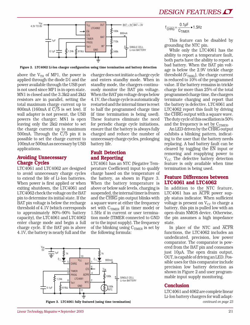
Linear Technology Magazine • September 2005 21
DESIGN FEATURES
above the VTH of MP1, the power is applied through the diode D1 and the power available through the USB port is not used since MP1 is in open state. MN1 is closed and the 3.3kΩ and 2kΩ resistors are in parallel, setting the total maximum charge current up to 800mA (160mA if C/5 is set low). If wall adapter is not present, the USB powers the charger; MN1 is open leaving only the 2kΩ resistor to set the charge current up to maximum 500mA. Through the C/5 pin it is possible to set the charge current to 100mA or 500mA as necessary by USB applications.
Avoiding Unnecessary Charge CyclesLTC4061 and LTC4062 are designed to avoid unnecessary charge cycles to extend the life of Li-Ion batteries. When power is first applied or when exiting shutdown, the LTC4061 and LTC4062 check the voltage on the BAT pin to determine its initial state. If the BAT pin voltage is below the recharge threshold of 4.1V (which corresponds to approximately 80%–90% battery capacity), the LTC4061 and LTC4062 enter charge mode and begin a full charge cycle. If the BAT pin is above 4.1V, the battery is nearly full and the
charger does not initiate a charge cycle and enters standby mode. When in standby mode, the chargers continu-ously monitor the BAT pin voltage. When the BAT pin voltage drops below 4.1V, the charge cycle is automatically restarted and the internal timer is reset to half the programmed charge time (if time termination is being used). These features eliminate the need for periodic charge cycle initiations, ensure that the battery is always fully charged and reduce the number of unnecessary charge cycles, prolonging battery life.
Fault Detection and ReportingLTC4061 has an NTC (Negative Tem-perature Coefficient) input to qualify charge based on the temperature of the battery, as shown in Figure 3. When the battery temperature is above or below safe levels, charging is suspended, the internal timer is frozen and the CHRG pin output blinks with a square wave at either the frequency set with CTIMER (if in timer mode) or 1.5Hz if in current or user termina-tion mode (TIMER connected to GND or to the input supply). The frequency of the blinking using CTIMER is set by the following formula:
fµF
CHzCHRG
TIMER= •0 1
1 5.
.
This feature can be disabled by grounding the NTC pin.
While only the LTC4061 has the ability to report a temperature fault, both parts have the ability to report a bad battery. When the BAT pin volt-age is below the 2.9V trickle charge threshold (VTRIKL), the charge current is reduced to 10% of the programmed value. If the battery remains in trickle charge for more than 25% of the total programmed charge time, the chargers terminate charging and report that the battery is defective. LTC4061 and LTC4062 report this fault by driving the CHRG output with a square wave. The duty cycle of this oscillation is 50% and the frequency is set by CTIMER.
An LED driven by the CHRG output exhibits a blinking pattern, indicat-ing to the user that the battery needs replacing. A bad battery fault can be cleared by toggling the EN input or removing and reapplying power to VCC. The defective battery detection feature is only available when time termination is being used.
Feature Differences between LTC4061 and LTC4062In addition to the NTC feature, LTC4061 has an ACPR power sup-ply status indicator. When sufficient voltage is present on VCC to charge a battery, this pin is pulled low with an open-drain NMOS device. Otherwise, the pin assumes a high impedance state.
In place of the NTC and A C P R functions, the LTC4062 includes an undedicated, precision, low power comparator. The comparator is pow-ered from the BAT pin and consumes just 10µA. The open drain output, OUT, is capable of driving an LED. Pos-sible uses for this comparator include precision low battery detection as shown in Figure 2 and user program-mable input supply monitoring.
ConclusionLTC4061 and 4062 are complete linear Li-Ion battery chargers for wall adapt-
+
CHRG
TIMERPROG
IDET
5
39
8
BAT
ACPR
NTC
1
2LTC4061
GND
100k
100kNTC11
619Ω
1.24k
1k 1k
800mA10
1µF
0.1µF
VIN5V
VIN
SINGLE CELLLi-Ion BATTERY
VCC
6
4C/5
Figure 3. LTC4061 fully featured (using time termination)
+
TIMERPROG
ENC/5
I
OUT
BAT
VIN4.3V TO 8V
IN+DET
LTC4062
GND1.24k 619Ω
100k
715k
348k
800mA
1µF
0.1µF
SINGLE CELLLi-Ion BATTERY
VCC BAT > 3V BAT < 3V
Figure 2. LTC4062 Li-Ion charger configuration using time termination and battery detection
continued on page 23

22 Linear Technology Magazine • September 2005
DESIGN FEATURES
IntroductionThe LTC3409 is a monolithic synchro-nous step-down regulator designed specifically to save space, improve battery life and simplify the design of 2-cell-alkaline, NiCd and NiMH pow-ered applications. It operates from a wide input voltage range, 1.6 to 5.5V, without the complexity and accompa-nying loss of efficiency of competing devices that require boost circuitry for generating internal voltages greater than VIN.
Space-saving features include an available 3mm × 3mm DFN package and a high, 1MHz to 3MHz, operating frequency, which allows the use of sur-face mount capacitors and inductors. To extend battery life, the LTC3409 of-fers two operating modes that improve light load efficiency, including Burst Mode operation, which consumes only 65μA of supply current at no load, and pulse skipping mode, which offers low ripple currents for noise-sensitive applications. Both modes consume less than 1μA quiescent current in shutdown.
The LTC3409 also features soft start, which limits inrush current at start-up.
Features
Soft StartTo reduce inrush currents at start-up, the LTC3409 offers a soft start function, which linearly ramps up the output voltage in about 1ms. For instance, the average output current required during soft start to charge a 10µF output capacitor to 1.8V in 1ms is 18mA. The total output current is the sum of the output capacitor charging current and the current delivered to the load as VOUT ramps up.
Monolithic Buck Regulator Operates Down to 1.6V Input; Simplifies Design of 2-Cell NiCd/NiMH Supplies
Switching Frequency SynchronizationThe LTC3409 offers an internally com-pensated phase locked loop (PLL) for switching frequency synchronization from 1MHz to 3MHz in addition to fixed frequencies of 1.7MHz and 2.6MHz. This high frequency range allows the use of surface mount capacitors and inductors.
The sync pin has three states: high, where the LTC3409 operates at a fixed 2.6MHz switching frequency; low, where the LTC3409 operates at a fixed 1.7MHz switching frequency; or as the input to the PLL, when the sync pin is toggled at a frequency of at least 1MHz for greater than 100µs. The SYNC pin threshold for PLL input is nominally
0.63V, thus allowing compatibility to low voltage logic interfaces.
Efficiency-Improving Operating ModesThe Mode pin has two states corre-sponding to two operating modes that improve efficiency at light loads: high for pulse skip mode, and low for Burst Mode operation. In pulse skipping mode, constant-frequency operation is maintained at lower load currents to decrease the output voltage ripple, and therefore reduce the chance of interference with audio circuitry. If the load current is low enough, cycle skipping eventually occurs to maintain regulation. Efficiency in pulse skipping mode is worse than Burst Mode op-
by Gregg Castellucci
EFFI
CIEN
CY (%
)
POW
ER L
OSS
(mW
)
LOAD CURRENT (mA)1k0.1
100
0
1k
11 10 100
100
10
1.8VIN
3.1VIN
2.5VIN
VOUT = 1.5V10
20
30
40
50
60
70
80
90
POWER LOSS AT 2.5VIN
Figure 2. Efficiency vs load current for the LTC3409 in pulse skip mode.
LOAD CURRENT (mA)
30
EFFI
CIEN
CY (%
)
90
100
20
10
80
50
70
60
40
0.1 10 100 1k0
1
1.8VIN
3.1VIN
2.5VIN
POWER LOSS AT 2.5VIN
VOUT = 1.5V
POW
ER L
OSS
(mW
)
1k
1
100
10
Figure 1. Efficiency vs load current for the LTC3409 in Burst Mode operation.
VFB
GND
VIN
VIN
SYNC
RUN
SW
MODE
LTC3409
L12.2µH
R1191k
C110pF
CIN4.7µF
VIN1.6V TO 5.5V
R2133k
VOUT1.5V0.6ACOUT
10µFCER
L1: SUMIDA CDRH2D18/LD
VIN FOR PULSE SKIP MODEGND FOR BURST MODE
Figure 3. 1.5V/600mA step down regulator

Linear Technology Magazine • September 2005 23
DESIGN FEATURES
eration at light loads, but comparable when the output load exceeds 50mA (see Figure 1 & 2).
In Burst Mode operation, the internal power MOSFETs operate intermittently based on load demand. Short burst cycles of normal switch-ing are followed by longer idle periods where the load current is supplied by the output capacitor. During the idle period, the power MOSFETs and any unneeded circuitry are turned off, reducing the quiescent current to 65µA. At no load, the output ca-pacitor discharges slowly through the feedback resistors resulting in very low frequency burst cycles that add only a few µA to the supply current. Burst Mode operation offers higher efficiency at low output currents than pulse skip mode, but when activated, Burst Mode operation produces higher output ripple than pulse skip mode.
Output Voltage ProgrammabilityThe LTC3409 output voltage is exter-nally programmed with two resistors to any value above the 0.613V inter-nal reference voltage, and is capable of 100% duty cycle. In dropout, the output voltage is determined by the input voltage minus the voltage drop
across the internal P-channel MOSFET and the inductor resistance.
Fault ProtectionThe LTC3409 protects against output over-voltage, output short-circuit and power over-dissipation conditions. When an over-voltage condition at the output (>10% above nominal) is sensed, the top MOSFET is turned off until the fault is removed. If the output is shorted to ground, reverse current in the synchronous switch is monitored to prevent inductor-current runaway. If the synchronous switch current is too high, the top MOSFET remains off until the synchronous switch current falls to a normal level.
When the junction temperature reaches approximately 160°C, the thermal protection circuit turns off the power MOSFETs allowing the part to cool. Normal operation resumes when the die temperature drops to 150°C.
1.5V/600mA Step-Down Regulator Using Ceramic CapacitorsFigure 3 shows an application of the LTC3409 using ceramic capacitors. This particular design supplies up to a 600mA load at 1.5V with an in-put supply between 1.8V and 3.1V. Ceramic capacitors have the advan-tages of small size and low equivalent series resistance (ESR), allowing very low ripple voltages at both the input and output. Because the LTC3409’s control loop does not depend on the output capacitor’s ESR for stable operation, ceramic capacitors can be used to achieve very low output ripple and small circuit size. Figures 4 and 5 show the transient response to a 50mA
to 600mA load step for the LTC3409 in pulse skip mode, and burst mode.
Efficiency ConsiderationsFigure 1 shows the efficiency curves for the LTC3409 (Burst Mode operation enabled) at various supply voltages. Burst Mode operation significantly lowers the quiescent current, result-ing in high efficiencies even with extremely light loads. Figure 2 shows the efficiency curves for the LTC3409 (pulse skipping mode enabled) at vari-ous supply voltages. Pulse skipping mode maintains constant-frequency operation at lower load currents. This necessarily increases the gate charge losses and switching losses, which impact efficiency at light loads. Ef-ficiency is still comparable to Burst Mode operation at higher loads.
ConclusionThe LTC3409 operates over a wide, 1.6V to 5.5V, input range, which al-lows it to operate from various power sources, from a 5V AC wall adapter to two series alkaline batteries. This flexible device is available in a 3mm × 3mm DFN package and includes a number of features to improve battery life and save space.
VOUT100mV/DIV
ILOAD500mA/DIV
20µs/DIV
INDUCTORCURRENT
500mA/DIV
Figure 4. LTC3409 transient response to a 50mA–600mA load step, pulse skip mode
VOUT100mV/DIV
ILOAD500mA/DIV
20µs/DIV
INDUCTORCURRENT
500mA/DIV
Figure 5. LTC3409 Transient response to a 50mA–600mA load step, Burst Mode operation
ers and USB sources. They extend lifetime of the batteries by avoiding un-necessary charge cycles. The LTC4061 and LTC4062’s versatility of charge
terminations, low quiescent current, simplicity, high level of integration and small size makes them an ideal choice for many portable USB applications.
LTC4061 and LTC4062 are available in a small 10-lead low profile 3mm x 3mm DFN package.
LTC4061/62, continued from page 21
For more information on parts featured in this issue, seehttp://www.linear.com/designtools
For more information on parts featured in this issue, seehttp://www.linear.com/designtools

24 Linear Technology Magazine • September 2005
DESIGN FEATURES
IntroductionMulti-voltage electronics systems are often saddled with complex power supply voltage tracking or sequenc-ing requirements, which, if not met, can result in system faults or even permanent failures in the field. The design difficulties in meeting these requirements are often compounded in distributed-power architectures where point-of-load (POL) DC/DC converters are scattered across PC board space, sometimes on different board planes. The problem is that power supply circuitry is often the last circuitry to be designed into the board, and it must be shoehorned into whatever little board real estate
Supply Tracking and Sequencing at Point-of-Load: Easy Design without the Drawbacks of MOSFETs
is left. Centralized sequencing-track-ing solutions can work well, but when no significant contiguous space is left on a board and the system specifica-tions are in flux, one wishes for a simple, drop-in, flexible option. That wish can be fulfilled with a tracking and sequencing solution that installs at the POL, and is tiny and versatile enough to be easily dropped into the board without disrupting the rest of the system design.
Wish GrantedThe LTC2927 provides a simple and versatile solution in a tiny footprint for
both tracking and sequencing without the drawbacks of series MOSFETs.
Each POL converter that must be tracked or sequenced can have a single LTC2927 placed at point-of-load as shown in Figure 1. By selecting a few resistors and a capacitor, the supplies are configured to ramp-up and ramp-down with a variety of volt-age profiles. Figure 2 shows various tracking and sequencing scenarios, including concurrent voltage tracking (Figure 2a), offset tracking (Figure 2b), ratiometric tracking (Figure 2c), and supply sequencing (Figure 2d).
Many voltage tracking solutions use series MOSFETs, which adds an in-
by Scott Jackson
RONB487k
RONA100k
ON RAMP MASTER
5VSLAVE 1
VCC
VIN
EARLYVIN6V
LTC2927
GND
FB
IN
LTC1628
FB = 0.8V OUTRAMPBUF
TRACK
0.1µF
CRAMP0.47µF
RTB1
RFB1105k
RFA120k
RTA1
ON RAMP
1.8VSLAVE 3
VCC
VINLTC2927
GND
FB
IN
LTC3728
FB = 0.8V OUTRAMPBUF
TRACK
RTB3
RFB326.1k
RFA320k
RTA3
ON RAMP
2.5VSLAVE 4
VCC
VINLTC2927
GND
FB
IN
LTC3728
FB = 0.8V OUTRAMPBUF
TRACK
RTB4
RFB463.4k
RFA420k
RTA4
ON RAMP
3.3VSLAVE 2
VCC
VIN
VIN
LTC2927
GND
FB
IN
LTC1628
FB = 0.8V OUTRAMPBUF
TRACK
RTB2
RFB263.4k
RFA220k
RTA2
VIN
VIN
Figure 1. Typical tracking application

Linear Technology Magazine • September 2005 25
DESIGN FEATURES
herent voltage drop, additional power consumption, and extra PC board real estate. Instead, the LTC2927 controls supplies by injecting current directly into the feedback nodes, thus controlling supply outputs without series MOSFETs. Figure 3 shows the simple “tracking cell” used to inject this
current. Furthermore, power supply stability and transient response remain unaffected because the injected current from the LTC2927 offsets the output voltage without altering the power supply control loop dynamics.
Power supply tracking is straight-forward with the LTC2927. A pair of
resistors configures the behavior of a slave supply relative to a master signal. The choice of resistors can cause a slave supply to track the master signal exactly or with a different ramp rate, voltage offset, time delay, or combina-tion of these.
A master signal is generated by tying a capacitor from the RAMP pin to ground or by supplying another ramping signal to be tracked as shown in Figure 1.
ExamplesConsider a complex tracking system. The schematic in Figure 1 uses an LTC1628 dual synchronous step-down converter to produce 5.0V and 3.3V supplies and an LTC3728 dual synchronous step-down converter to produce 2.5V and 1.8V supplies from a 6.0V input. Four LTC2927s con-nected to the feedback nodes control the ramp-up and ramp-down behav-ior of these supplies. An early VIN is supplied to the devices to guarantee correct operation prior to tracking the supplies.
The specification calls for the 5.0V and 3.3V supplies to track coincidently at ~20V/s, the 1.8V supply should ramp up quickly at 100V/s after the 3.3V supply reaches 2.0V, and the 2.5V supply should ramp up at the same rate as the 1.8V supply, but delayed by 20ms. The LTC2927 data sheet (available at www.linear.com) includes a 3-step design procedure that is fol-lowed for each supply. When using that procedure, use the following for equation (1) in Step 1, with a master signal ramp-rate SM of 20V/s:
C AV s
FRAMP = ≈1020
0 47µ µ.
5V and 3.3V Supply Coincident TrackingBecause the master ramp rate is cho-sen to be equal to the desired ramp rate of the 5V and 3.3V supplies, coincident tracking is selected. If the feedback voltage of the switching power supply is 0.8V, as it is on the LTC1628, then coincident tracking can be configured by setting the tracking resistors equal to the feedback resistors (verified by
MASTER
SLAVE1
SLAVE2
MASTER
SLAVE1
SLAVE2
MASTER
SLAVE1
SLAVE2
MASTER
SLAVE1
SLAVE2
a. Coincident tracking
a. Offset tracking
c. Ratiometric tracking
d. Supply sequencing
Figure 2. Types of power supply voltage tracking

26 Linear Technology Magazine • September 2005
DESIGN FEATURES
the TRACK and FB pins. Therefore, confirm that less than 1mA flows from TRACK when VMASTER is at 0V.
I VR R
mA mA
TRACKTRACK
TA TB1
1 1
0 05 1
=
= <||
.
I VR R
mA mA
TRACKTRACK
TA TB2
2 2
0 05 1
=
= <||
.
I VR R
mA mA
TRACKTRACK
TA TB3
3 3
0 45 1
=
= <||
.
I VR R
mA mA
TRACKTRACK
TA TB4
4 4
0 24 1
=
= <||
.
The connections between each LTC2927 shown in Figure 1 allow extra control for each supply. With this system, the 3.3V supply uses the 5V supply as its master signal. If for some reason the 5V supply should col-lapse, the 3.3V supply follows it down. Likewise, the 1.8V and 2.5V supplies use the 3.3V supply as their master signal and track it up and down.
following Step 2 of the 3-Step Design Procedure),From equation (2) of the 3-Step Design Procedure:RTB1 = RFB1 = 105kΩ RTB2 = RFB2 = 63.4kΩ
From Equation (3) of the 3-Step Design Procedure:RTA1ʹ = RFA1 = 20kΩ RTA2ʹ = RFA2 = 20kΩ
In the 3-step design procedure RTAʹ represents the value of RTA that pro-duces no delay or offset. Since no delay is desired, RTA = RTAʹ, and Step 3 of the Design procedure is unnecessary.
1.8V and 2.5V Supply SequencingThe 1.8V supply ramps up 2V below the 3.3V supply but at a ramp rate of 100V/s. Set the slave ramp rate to 100V/s in equation (2) to find RTB3:
R kV sV s
kTB3 26 121 3100
56 2= ≈..
.Ω Ω
Complete Step 2 by solving for RTA3ʹ using equation (3).R kTA3 10 755′ = − . Ω
Step 3 adjusts RTA3 for the desired delay between the 3.3V supply and the 1.8V supply. An offset of 2V results in a delay of ~100ms for the ramp rate chosen.
R k
R R Rk
TA
TA TA TA
3
3 3 3
2 09
2 61
″ =
= ′ ″
≈
.
||.
Ω
Ω
The 2.5V supply has the same ramp rate as the 1.8V supply, but
0.8V
–
+
2927 F05
5FB
5TRACK
VCC
MASTER
SLAVEFB OUT
DC/DCRTB
RFBRFA
RTA
+–
Figure 3. Simplified tracking cell
RONB487k
RONA100k
ON RAMP MASTER
DMMT5551
–5VSLAVE
VCC
VIN
EARLYVIN6V
LTC2927
GND
FB
IN
LTC3462
FB = 0V
VREF = 1.25V
OUT
RAMPBUF
TRACK
0.1µF
CRAMP0.1µF
RTB1137k
RFB274k
RFA/234k
RFA/234k
RTA126.1k
Figure 5. Supply tracking of GND referenced negative regulator
5V
3.3V2.5V1.8V
1V/DIV
50ms/DIV
Figure 4. Output profile of the circuit in Figure 1
is delayed another 20ms. Repeating Step 2 and Step 3 for the 2.5V supply results in:
R kV sV s
kTB4 43 221 3100
93 1= ≈..
.Ω Ω
R kTA4 28 052′ = − . Ω R k
R R Rk
TA
TA TA TA
4
4 4 4
28 8
3 24
″ =
= ′ ″
≈
.
||.
Ω
Ω
The tracking profile for this system is shown in Figure 4.
Note that not every combination of ramp-rates and delays is possible. Small delays and large ratios of slave ramp rate to master ramp rate may result in solutions that require nega-tive resistors. In such cases, either the delay must be increased or the ratio of slave ramp rate to the master ramp rate must be reduced. In addition, the chosen resistor values should not require more than 1mA to flow from

Linear Technology Magazine • September 2005 27
DESIGN FEATURES
Negative Supply TrackingIt is possible to track negative voltage regulators with the LTC2927. Figure 5 shows a tracking example using a LT3462 inverting DC/DC converter to produce a –5V supply. This converter has a ground-based reference, which allows current to be pulled from a node where RFA has been divided in two. To properly pull current from the LT3462 FB network, a current mirror must be placed between the LTC2927 and the converter. The 3-Step design
0VSLAVE
–VMASTER
–5V SLAVE–VMASTER
1V/DIV
10ms/DIV
0V
–5V SLAVE–VMASTER
1V/DIV
10ms/DIV
a. Tracking error due to current mirror pull-down limitation
b. Tracking without current mirror pull-down limitation
Figure 6. Output profile of circuit of Figure 9
procedure remains the same with minor modifications to equations (2) and (3):
R R SSTB
FB M
S= •
2
R VVR
VR
TATRACK
REF
FA
TRACK
TB
′ =−2
All other equations remain the same.
Figure 6a shows the tracking profile of Figure 5 with a ramp rate of 100V/s. VMASTER is positive, but the inverse is shown for clarity. The –5V slave does not pull all the way up to 0V at VMAS-
TER = 0V. This is because the ground referenced current mirror cannot pull its output all the way to ground. If the converter has a FB reference voltage greater than 0V or if a negative supply is available for the current mirror, the error can be removed. The resulting waveform is shown in Figure 6b.
ConclusionThe LTC2927 simplifies power supply tracking and sequencing by offer-ing superior performance in a tiny point-of-load area. A few resistors can configure simple or complex supply behaviors. Series MOSFETs are elimi-nated along with their parasitic voltage drops and power consumption. The LTC2927 offers all of these features in a tiny 8-lead ThinSOT™ and 8-lead (3mm × 2mm) DFN package.
ESR generates a loop zero at 5kHz to 50kHz that is instrumental in giving acceptable loop phase margin. Ce-ramic capacitors remain capacitive to beyond 300kHz and usually resonate with their ESL before ESR becomes effective. Also, ceramic caps are prone to temperature effects, requiring the designer to check loop stability over the operating temperature range. For these reasons, great care must be taken when using only ceramic input and output capacitors. The LTC3417 helps solve loop stability problems with its OPTI-LOOP phase compensa-tion adjustment, allowing the use of ceramic capacitors. For details, and a process for optimizing compensation components, see Linear Technology Application Note 74 (AN76).
Although the LTC3417 is capable of operating at 4MHz, the frequency in this application is set for 1.5MHz by connecting the FREQ pin to VIN.
Figures 5 through 7 show the trade off between mode and VOUT ripple noise. Figure 5 shows the voltage
ripple at VOUT1 and the current through the inductor while the LTC3417 is in Burst Mode operation. The ripple voltage in this example was taken at an ILOAD of 40mA and is only 15mVP–P. The worst case output voltage ripple occurs just before the part switches from bursting to continuous mode, which occurs at about 250mA. At his point, the VOUT ripple can be as high as 25mVP–P.
Figure 6 shows the VOUT1 ripple and the current through the inductor when the part is in Pulse Skipping Mode. Notice that the current through the inductor does go slightly negative, and then produces some high frequency components. The higher frequency components are due to the switching MOSFETS turning off. At lower cur-rents, the part starts skipping pulses, and thus produces some lower fre-quency components. In this case, the voltage ripple does indeed show some higher frequency components, yet the ripple itself is at about 5mVP–P.
Figure 7 shows the voltage ripple at VOUT1 and the inductor current
when the part is in Forced Continu-ous mode. Notice that the current through the inductor goes negative. At no time, during Forced Continuous doe the MOSFETS actually turn off, they keep switching. Therefore, the frequency component of the voltage ripple stays constant at the operating frequency. The voltage ripple therefore looks constant and stays below 5mV over all load currents.
ConclusionThe LTC3417 is a dual synchronous, step-down, current mode, DC/DC con-verter designed to fit in the tight spaces afforded by today’s portable devices. Switching MOSFETS are integrated into the device, and high frequency operation enables the use of small sized components. It is also designed with versatility in mind with external components for loop compensation, variable frequency operation and dif-ferent operating modes to optimize efficiency and noise.
LTC3417, continued from page 8

28 Linear Technology Magazine • September 2005
DESIGN FEATURES
exceeds the maximum current sense threshold, pulse skipping occurs.
The LT3724 also incorporates a programmable soft-start that controls the slew rate of the converter output voltage during startup to reduce sup-ply inrush currents and output voltage overshoot.
The gate driver is capable of driv-ing large, low RDS(ON), standard level, n-channel MOSFETS without the need for a gate drive buffer. The driver uses a bootstrapped supply rail which allows it to drive either a high side MOSFET, as found in buck converters, or a low side MOSFET, as found in boost converters.
On-Board RegulatorThe LT3724’s internal 8V linear regulator eliminates the need for an external regulator or a slow-charge hysteretic start scheme. This regulator generates the local supply that powers the IC (VCC), from the converter input supply, VIN.
The on-board regulator can oper-ate the IC continuously, provided the input voltage and/or FET gate charge currents are low enough to avoid ex-cessive power dissipation in the part.
IntroductionThe LT3724 is a single-switch DC/DC controller that can be used in medium power step-down, step-up, inverting and SEPIC converter topologies. It offers simple solutions to regulating system voltages at high efficiencies over a wide input voltage range (4V–60V) and wide load range.
LT3724 Features The LT3724 uses a 200kHz fixed-fre-quency current-mode architecture. An internal high voltage bias regulator allows for simple startup and biasing, and it can be back driven by the output to increase supply efficiency and lower power dissipation in the IC.
User selectable Burst Mode opera-tion can maintain high efficiency over a wide load range. In Burst Mode op-eration quiescent current is reduced to under 100µA, making the LT3724 ideal for use in applications with supply maintenance requirements or light load and no-load conditions. A precision shutdown pin threshold allows for easy supply under voltage lockout where quiescent currents are reduced to less than 10µA.
Supply short circuit control is via an external sense resistor, through which the LT3724 continuously monitors in-ductor current. If the inductor current
Common practice uses the on board regulator during startup and then back drives the VCC pin above its 8V regulated voltage during operation. This reduces the power dissipation in the IC and increases converter ef-ficiency. The LT3724 has a start-up requirement of VIN ≥ 7.5V. This assures that the on-board regulator brings the VCC pin above its undervoltage lockout threshold of 6.25V. If VCC is maintained using an external supply, such as the converter output, the LT3724 can continue to operate with VIN as low as 4V.
Burst Mode OperationThe LT3724 employs low-current Burst Mode operation to maximize ef-
Versatile Controller Simplifies High Voltage DC/DC Converter Designs
by Tom Sheehan
VIN
SHDN
CSS
Burst_EN
VFB
VC
SGND
BOOST
TG
SW
VCC
PGND
SENSE+
SENSE–
VIN30V TO
60V
VOUT24V75W
LT37241M
52.3k
1000pF
4.99k 93.1k
200k
0.22µF
COUT330µF
CIN68µF
1µF
47µH
0.025ΩSi7852
SS3H9BAS19
120pF680pF
40.2k
+
Figure 1. 30V–60V to 24V 75W DC/DC converter with input UVLO and full time usage of on board high voltage regulator
LOAD CURRENT (A)0.1
EFFI
CIEN
CY (%
)
POWER LOSS (W
)
95
90
85
80
75
70
65
12
10
8
6
4
2
01 10
VIN = 48V
LOSS
EFFICIENCY
Figure 2. 30V–60V to 24V, 75W DC/DC converter efficiency and power loss
VOUT5V/DIV
2.5ms/DIV
Figure 3. 30V–60V to 24V, 75W DC/DC converter output soft-start waveform

Linear Technology Magazine • September 2005 29
DESIGN FEATURES
ficiency during light-load and no-load conditions. Burst Mode is enabled by shorting the BURST_EN pin to SGND and can be disabled by shorting BURST_EN to VFB.
When the required switch current, sensed via the VC pin voltage, is below 15% of programmed current limit, the Burst Mode function is engaged. During the Burst interval, switching ceases and all internal IC functions are disabled, with the exception of the VCC regulator, error amplifier, and bandgap reference. Current at the VIN pin is reduced to 20µA and VCC cur-rent is reduced to 80µA. If no external
drive is provided for VCC, all VCC bias currents originate from the VIN pin, giving a total VIN current of 100µA. An internal negative-excursion clamp on the VC pin is set at 100mV below the switch disable threshold, limiting the negative excursion of the pin volt-age and minimizing converter output ripple during Burst Mode operation.
Precision Shutdown ThresholdThe LT3724 SHDN pin is used for precision shutdown in analog monitor-ing applications, as well as logic-level controlled applications. Input sup-ply undervoltage lockout for supply
sequencing or start-up over-current protection is easily achieved by driving
4
R34.7M
R640.2k
R2187k
R110k
VIN
SHDN
CSS
BURST_EN
VFB
VC
SGND
BOOST
TG
SW
VCC
PGND
SENSE+
SENSE–
M1
D2SBM540
LT3724
1
3
5
6
7
8
16
15
14
12
11
10
9
C34700pF
C2120pF
C41µF25V
C11500pF
0.1µF25V
COUT1330µF35V
COUT22.2µF x350V
CIN = SANYO, 25SVP33ML1 = VISHAY, IHLP-5050FD-011M1 = SILICONIX, Si7370DPCOUT1 = SANYO, 35CV330AXACOUT2 = TDK, C4532X7R1H225KD2 = DIODESINC., SBM540RSENSE = IRC LRF2512-01-R0I5-F
CIN33µF ×225V
VIN8V TO16V
RSENSE0.015Ω
L110µH
VOUT24V AT 50W
RCSS200k
D1BAV99
Figure 6. 12V to 24V/50W boost converter
LOAD CURRENT (A)0.1
EFFI
CIEN
CY (%
)
POWER LOSS (W
)
92
91
90
89
88
87
86
85
3.5
3.0
2.5
2.0
1.5
1.0
0
0.5
1 10
VIN = 20V
VIN = 10V
VIN = 15V
LOSSVIN = 15V
Figure 5. 15V to 12V 25W SEPIC DC/DC converter efficiency and power loss
Figure 4. 15V to 12V 25W SEPIC DC/DC converter
4
RA100k
R510k
RSENSE0.010Ω
R2130k
R114.7k
SHDN
CSS
R3200k
BURST_EN
VFB
VC
SGND
TG
SW
VCC
PGND
SENSE+
SENSE–
1
3
5
6
7
8
16
15
14
12
11
10
9
C32200pF
C2120pF
R447k
C70.1µF
C1390pF
CIN225V1µF
CIN122µF2x25V
VIN4.5V TO 20V
60V TRANSIENT
D1AGSD2004
D3D1N4148
L120µH
L120µH
D1BGSD2004
D2
VOUT12V AT 25W
COUT222µF
M1
VIN BOOST
LT3724
C41µF25V
COUT1330µF
25V
16VC656pF
R710Ω
R610Ω
C522µF
3x25V
•
•
C5, CIN1, COUT2 = TDKC453X7R1E226MCOUT1 = SANYO, OS-CON 16SVP330MD2 = ON SEMI, MBRD660L1 = COILCRAFT VERSAPAC VP5-D83M1 = VISHAY, Si7852DP

30 Linear Technology Magazine • September 2005
DESIGN FEATURES
the SHDN pin with a resistor divider from the VIN supply, such that the divider output is 1.35V when VIN is at the desired undervoltage lockout rising threshold voltage. 120mV of input hysteresis on the SHDN pin al-lows the IC to withstand almost 10% of input supply droop before disabling the converter. The SHDN pin has a secondary threshold of 0.5V, below which the IC operates in an ultra-low-current shutdown mode with IVIN < 10 µA. The shutdown function can be disabled by connecting the SHDN pin to VIN through a large value pull-up resistor.
Continuous High-Side Inductor Current SensingThe LT3724 uses a wide common-mode input range current sense amplifier that operates over a 0V to 36V range. This current sense amplifier provides continuous inductor current sensing via an external sense resistor. This scheme does not require blank-ing intervals or a minimum on-time to monitor current, an advantage over schemes that sense switch current. The sense amplifier monitors inductor current independent of switch state, so the main switch is not enabled unless the inductor current is below the current that corresponds to the VC pin voltage. This “turn-on” deci-sion is performed at the start of each cycle, and individual switch cycles are skipped should an over-current condi-tion occur. This eliminates many of the potential over-current dangers caused by minimum on-time requirements, such as those that can occur during startup, short-circuit, or abrupt input transients.
Current Mode ControlThe LT3724 uses current mode control architecture enabling a higher supply bandwidth thereby improving line and load transient response. Current mode control also requires fewer compensa-tion components than voltage mode control architectures, making it much easier to compensate over all operating conditions.
Soft StartThe LT3724 employs an adaptive soft-start scheme that directly controls the rising rate of DC/DC converter output voltage. Output voltage overshoot and inrush current are well controlled with this method. This rising rate of the output voltage is programmed with a capacitor connected to the converter output, where:2µA = COUT • (Desired ΔV/Δt)
The soft-start function maintains this desired output rising rate up to 95% of the regulated output voltage. The soft-start function is re-enabled if the converter output droops below 70% regulation, so converter recov-ery is graceful from a short-duration shutdown or an output short-circuit condition.
ApplicationsThe applications here present only a small sample of what can be accom-plished with the LT3724. See the data sheet at www.linear.com for more, including an inverting converter.
30V–60V to 24V, 75W DC/DC ConverterFigure 1 shows a 30V–60V to 24V, 75W converter configured for supply input undervoltage lockout and full time usage of the onboard high volt-age bias regulator. This application demonstrates how a high efficiency supply can be built inexpensively and with fewer than 20 components. Figure 2 shows the converter efficiency and power loss vs load current.
Power for the IC is obtained di-rectly from VIN through the LT3724’s internal VCC regulator. VIN UVLO is programmed via a resistor divider to enable the LT3724 at 90% of the specified low end of VIN range, or 27V, which corresponds to the SHDN pin voltage exceeding 1.35V. The SHDN input has 120mV of hysteresis, so the converter is disabled if VIN drops below 24V.
The LT3724 soft-start function controls the rising slew rate of the output voltage at startup such that the current through the soft start capacitor is 2µA, so the converter output rises at a controlled rate of 2µA/1nF, or 2V/mS. Figure 3 shows the soft start ramp.
4V–60V to 12V, 2A SEPIC ConverterIn LT3724 converter applications with output voltages in the 9V to 20V range, back-feeding VCC from the converter output is accomplished by connecting a diode from the supply output to the VCC pin. Figure 4 shows a 15V to 12V, 2A SEPIC converter configured to use the 12V output voltage to back drive VCC. This application also shows the versatility of the LT3724 by configur-ing it to control a SEPIC converter. SEPIC converters are used where the input voltage can be both less than or greater than the output voltage, such as a battery powered application.
In some DC/DC converter applica-tions, the converter must withstand or operate through intermittent input voltage excursions. This is typical of automotive battery-voltage ap-plications, where high voltage line transients such as load-dump or low voltage transients such as startup must be accommodated. This con-verter design is optimized to operate with a 15V nominal input voltage but can regulate the output voltage over a wide input range of 4V to 60V. Figure 5 shows the converter efficiency and power loss vs load current.
This converter also uses an external current limit fold-back scheme. This fold-back circuit consists of a single 1N4148 diode (D2) and a resistor (R5).
LOAD CURRENT (A)0.1
EFFI
CIEN
CY (%
)POW
ER LOSS (W)
100
98
96
94
92
90
88
3.0
2.5
2.0
1.5
1.0
0
0.5
1 10
VIN = 8V
VIN = 12V
VIN = 16V
LOSSVIN = 12V
Figure 7. 12V to 24V/50W boost converter efficiency and power loss
continued on page 34
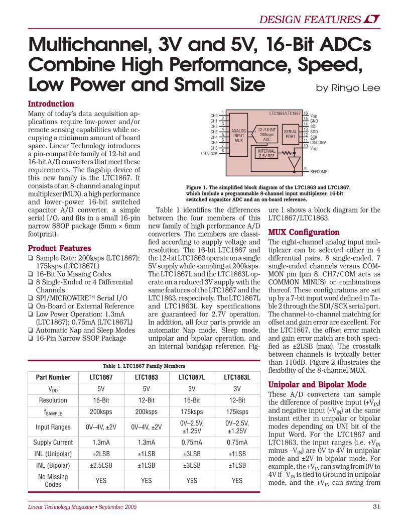
Linear Technology Magazine • September 2005 31
DESIGN FEATURES
IntroductionMany of today’s data acquisition ap-plications require low-power and/or remote sensing capabilities while oc-cupying a minimum amount of board space. Linear Technology introduces a pin-compatible family of 12-bit and 16-bit A/D converters that meet these requirements. The flagship device of this new family is the LTC1867. It consists of an 8-channel analog input multiplexer (MUX), a high performance and lower-power 16-bit switched capacitor A/D converter, a simple serial I/O, and fits in a small 16-pin narrow SSOP package (5mm × 6mm footprint).
Product Features Sample Rate: 200ksps (LTC1867);
175ksps (LTC1867L) 16-Bit No Missing Codes 8 Single-Ended or 4 Differential
Channels SPI/MICROWIRE™ Serial I/O On-Board or External Reference Low Power Operation: 1.3mA
(LTC1867); 0.75mA (LTC1867L) Automatic Nap and Sleep Modes 16-Pin Narrow SSOP Package
Multichannel, 3V and 5V, 16-Bit ADCs Combine High Performance, Speed, Low Power and Small Size
Table 1 identifies the differences between the four members of this new family of high performance A/D converters. The members are classi-fied according to supply voltage and resolution. The 16-bit LTC1867 and the 12-bit LTC1863 operate on a single 5V supply while sampling at 200ksps. The LTC1867L and the LTC1863L op-erate on a reduced 3V supply with the same features of the LTC1867 and the LTC1863, respectively. The LTC1867L and LTC1863L key specifications are guaranteed for 2.7V operation. In addition, all four parts provide an automatic Nap mode, Sleep mode, unipolar and bipolar operation, and an internal bandgap reference. Fig-
ure 1 shows a block diagram for the LTC1867/LTC1863.
MUX ConfigurationThe eight-channel analog input mul-tiplexer can be selected either in 4 differential pairs, 8 single-ended, 7 single-ended channels versus COM-MON pin (pin 8, CH7/COM acts as COMMON MINUS) or combinations thereof. These configurations are set up by a 7-bit input word defined in Ta-ble 2 through the SDI/SCK serial port. The channel-to-channel matching for offset and gain error are excellent. For the LTC1867, the offset error match and gain error match are both speci-fied as ±2LSB (max). The crosstalk between channels is typically better than 110dB. Figure 2 illustrates the flexibility of the 8-channel MUX.
Unipolar and Bipolar ModeThese A/D converters can sample the difference of positive input (+VIN) and negative input (–VIN) at the same instant either in unipolar or bipolar modes depending on UNI bit of the Input Word. For the LTC1867 and LTC1863, the input ranges (i.e. +VIN minus –VIN) are 0V to 4V in unipolar mode and ±2V in bipolar mode. For example, the +VIN can swing from 0V to 4V if –VIN is tied to Ground in unipolar mode, and the +VIN can swing from
by Ringo Lee
CH0CH1CH2CH3CH4CH5CH6
CH7/COM
12345678
16151413121110
VDDGNDSDISDOSCKCS/CONVVREF
12-/16-BIT200ksps
ADC
+–
SERIALPORT
ANALOGINPUTMUX
REFCOMP9
INTERNAL2.5V REF
LTC1863/LTC1867
Figure 1. The simplified block diagram of the LTC1863 and LTC1867, which include a programmable 8-channel input multiplexer, 16-bit switched capacitor ADC and an on-board reference.
Table 1. LTC1867 Family Members
Part Number LTC1867 LTC1863 LTC1867L LTC1863L
VDD 5V 5V 3V 3V
Resolution 16-Bit 12-Bit 16-Bit 12-Bit
fSAMPLE 200ksps 200ksps 175ksps 175ksps
Input Ranges 0V–4V, ±2V 0V–4V, ±2V 0V–2.5V, ±1.25V
0V–2.5V, ±1.25V
Supply Current 1.3mA 1.3mA 0.75mA 0.75mA
INL (Unipolar) ±2LSB ±1LSB ±3LSB ±1LSB
INL (Bipolar) ±2.5LSB ±1LSB ±3LSB ±1LSB
No Missing Codes YES YES YES YES
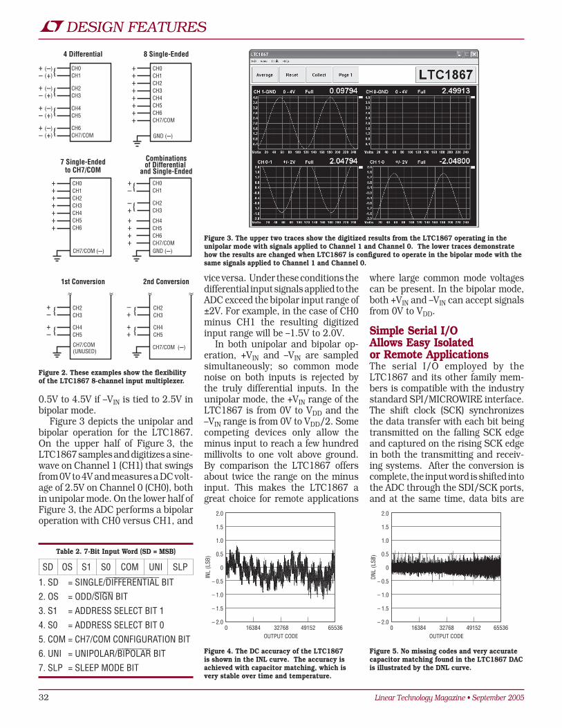
32 Linear Technology Magazine • September 2005
DESIGN FEATURES
0.5V to 4.5V if –VIN is tied to 2.5V in bipolar mode.
Figure 3 depicts the unipolar and bipolar operation for the LTC1867. On the upper half of Figure 3, the LTC1867 samples and digitizes a sine-wave on Channel 1 (CH1) that swings from 0V to 4V and measures a DC volt-age of 2.5V on Channel 0 (CH0), both in unipolar mode. On the lower half of Figure 3, the ADC performs a bipolar operation with CH0 versus CH1, and
vice versa. Under these conditions the differential input signals applied to the ADC exceed the bipolar input range of ±2V. For example, in the case of CH0 minus CH1 the resulting digitized input range will be –1.5V to 2.0V.
In both unipolar and bipolar op-eration, +VIN and –VIN are sampled simultaneously; so common mode noise on both inputs is rejected by the truly differential inputs. In the unipolar mode, the +VIN range of the LTC1867 is from 0V to VDD and the –VIN range is from 0V to VDD/2. Some competing devices only allow the minus input to reach a few hundred millivolts to one volt above ground. By comparison the LTC1867 offers about twice the range on the minus input. This makes the LTC1867 a great choice for remote applications
where large common mode voltages can be present. In the bipolar mode, both +VIN and –VIN can accept signals from 0V to VDD.
Simple Serial I/O Allows Easy Isolated or Remote ApplicationsThe serial I/O employed by the LTC1867 and its other family mem-bers is compatible with the industry standard SPI/MICROWIRE interface. The shift clock (SCK) synchronizes the data transfer with each bit being transmitted on the falling SCK edge and captured on the rising SCK edge in both the transmitting and receiv-ing systems. After the conversion is complete, the input word is shifted into the ADC through the SDI/SCK ports, and at the same time, data bits are
Table 2. 7-Bit Input Word (SD = MSB)
SD OS S1 S0 COM UNI SLP
1. SD = SINGLE/DIFFERENTIAL BIT2. OS = ODD/SIGN BIT3. S1 = ADDRESS SELECT BIT 14. S0 = ADDRESS SELECT BIT 05. COM = CH7/COM CONFIGURATION BIT6. UNI = UNIPOLAR/BIPOLAR BIT7. SLP = SLEEP MODE BIT
OUTPUT CODE0
INL
(LSB
)
4915216384 32768 65536
2.0
1.5
1.0
0.5
0
– 0.5
– 1.0
– 1.5
– 2.0
Figure 4. The DC accuracy of the LTC1867 is shown in the INL curve. The accuracy is achieved with capacitor matching, which is very stable over time and temperature.
OUTPUT CODE0
DNL
(LSB
)
4915216384 32768 65536
2.0
1.5
1.0
0.5
0
– 0.5
– 1.0
– 1.5
– 2.0
Figure 5. No missing codes and very accurate capacitor matching found in the LTC1867 DAC is illustrated by the DNL curve.
Figure 3. The upper two traces show the digitized results from the LTC1867 operating in the unipolar mode with signals applied to Channel 1 and Channel 0. The lower traces demonstrate how the results are changed when LTC1867 is configured to operate in the bipolar mode with the same signals applied to Channel 1 and Channel 0.
Figure 2. These examples show the flexibility of the LTC1867 8-channel input multiplexer.
CH0CH1CH2CH3CH4CH5CH6CH7/COM
GND (–)
8 Single-Ended
+++++++
4 Differential
+ (–) +
CH0CH1CH2CH3CH4CH5CH6
CH7/COM (–)
7 Single-Endedto CH7/COM
+++++++
+ (–)
+ (–)
+ (–)– (+)
– (+)
– (+)
– (+)
GND (–)
Combinationsof Differential
and Single-Ended
+++++
+––
CH0CH1
CH2CH3
CH4CH5
CH6CH7/COM
CH0CH1
CH2CH3
CH4CH5CH6CH7/COM
CH7/COM (UNUSED)
CH7/COM (–)
1st Conversion 2nd Conversion
+–+–
+–
++
CH2CH3
CH4CH5
CH2CH3
CH4CH5

Linear Technology Magazine • September 2005 33
DESIGN FEATURES
delivers 16-bit, no missing codes performance with an accurate INL specification of ±2LSB(max) in uni-polar mode and ±2.5LSB(max) in bipolar mode. Typical INL and DNL plots for LTC1867 versus output code are shown in Figures 4 and 5. This performance is achieved with capaci-tor matching which is very stable over time and temperature.
Along with outstanding DC perfor-mance, the LTC1867 also has very good AC performance. The signal-to-noise ratio (SNR) is typically 89dB with an input range of 4V and improves to 90.5dB when an external reference
released through the SDO/SCK ports. The A/D converter starts to acquire the analog input signals after reading in the 7-bit Input Word. These ADCs have an internally trimmed conver-sion clock which allows the sampling frequency to approach DC without affecting the conversion results. The 4-wire interface allows the LTC1867 and its siblings to fit well with isolated or remotely located applications.
Outstanding DC and AC PerformanceOperating from a 5V supply and sam-pling up to 200ksps, the LTC1867
R2
R3
REFERENCEAMP
10µF
2.2µF
REFCOMP
GND
VREF
R16k10
9
15
2.5V
4.096V
LTC1863/LTC1867
BANDGAPREFERENCE
10
0.1µF10µF
LT1019A-2.5VOUT
VIN
5V
VREF
LTC1863/LTC1867
GND
REFCOMP
15
9
+
2.2µF
Figure 6. LTC1863/LTC1867 reference circuit. The internal reference can be overdriven by an external Reference, LT1019A-2.5 for better drift and/or accuracy performance.
fSAMPLE (ksps)1
SUPP
LY C
URRE
NT (m
A)2.0
1.5
1.0
0.5
010 100 1000
VDD = 5V
Figure 7. The LTC1867 features an Automatic Nap mode that cuts the power dissipation as the sampling frequency is reduced.
S0SD 0S S1 COM UNI SLP
MSB = D11 D10 D9 D8 D7 D6 D5 D4 D3 D2 D1 D0
CS/CONV
SCK
SDI
SDO(LTC1867)
Hi-Z
1 2 3 4 5 6 7 8 9 10 11 12 13 14 15 16
tCONV
D12MSB = D15 D14 D13 D11 D10 D9 D8 D7 D6 D5 D4 D3 D2 D1 D0Hi-Z
tCONV
DON'T CAREDON'T CARE
NOT NEEDED FOR LTC1863
tACQ
SDO(LTC1863)
Figure 9. The Automatic Nap mode is not activated if the CS/CONV pulse is shorter than the conversion time. After the conversion the ADC remains powered up.
S0SD 0S S1 COM UNI SLP
D11 D10 D9 D8 D7 D6 D5 D4 D3 D2 D1 D0
1/fSCK
CS/CONV
SCK
SDI
SDO(LTC1863)
Hi-Z
D12D15 D14 D13 D11 D10 D9 D8 D7 D6 D5 D4 D3 D2 D1 D0Hi-Z
1 2 3 4 5 6 7 8 9 10 11 12 13 14 15 16
DON'T CAREDON'T CARE
NOT NEEDED FOR LTC1863tCONV NAP MODE
SDO(LTC1867)
MSB
MSB
Figure 8. The Automatic Nap mode provides power reduction at reduced sample rates. This feature is activated when CS/CONV remains high after the conversion is completed.

34 Linear Technology Magazine • September 2005
DESIGN FEATURES
voltage of 5V is applied to the REF-COMP pin (tie VREF pin to 0V to turn off internal reference buffer).
Internal ReferenceThis family has an on-chip, tem-perature compensated, curvature corrected, bandgap reference that is factory trimmed to 2.5V for the LTC1867 and the LTC1863, and 1.25V for the LTC1867L and the LTC1863L. The reference is internally connected to a reference amplifier and is avail-able at VREF (Pin 10). A 6kΩ resistor in the LTC1867 and the LTC1863 (3kΩ resistor for the LTC1867L and the LTC1863L) is in series with the output so that it can be easily over-driven by an external reference if better drift and/or accuracy are required as shown in Figure 6. The reference am-plifier gains the VREF voltage by 1.638 to 4.096V at REFCOMP (Pin 9). This reference amplifier compensation pin, REFCOMP, must be bypassed with a 10µF ceramic or tantalum in parallel with a 0.1µF ceramic for best noise performance.
Low Power Improves Battery LifeThe LTC1867 and LTC1863 consume only 1.3mA at a sampling rate of 200ksps. As the sampling frequency is reduced, the converters use even less
supply current with the automatic Nap feature. For example, the parts draw only 760µA and 200µA at sampling frequencies of 100ksps and 10ksps, respectively.
Automatic Nap mode is active when the CS/CONV pulse width is longer than the conversion time of the A/D converter. The part goes to Nap mode automatically right after a conversion is completed and remains powered down (the ADC draws 150µA in Nap mode) as long as the CS/CONV stays HIGH after conversion. The internal reference, however, is still active and provides a 2.5V output. In this way, the LTC1867/LTC1863 requires no additional wake up time before the next conversion is started. Figure 7 shows how the supply current is greatly re-duced as the sample rate is decreased when using this feature.
The ADCs can also go into the Sleep mode during long inactive periods. In sleep mode the internal reference is also powered down, thus reducing the draw to leakage currents of less than 1μA. The wake up time out of the sleep mode is determined by how fast the reference bypass capacitors can be charged. The wake up time can be estimated with the values of bypass capacitor on VREF and the on-chip resistor between the internal reference and VREF pin. For the 16-bit
LTC1867L, the wake up time can be estimated as:(resistor value) • (bypass capacitor value) • (number of time constant needed to settle to 16-bit accuracy)or (3k • 2.2µF • 11).
Typically with bypass capacitors of 2.2µF and 10µF on the VREF and REFCOMP pins, this takes about 80ms for LTC1867L. However, if an external reference is used, the wake up time is less than 10ms.
When the CS/CONV pulse is shorter than the conversion time, the ADCs stay powered up and the Automatic Nap mode is not activated. In this configuration, the digital output, SDO, becomes active after the conversion is completed. Figures 8 and 9 show the timing diagrams for the two cases described.
ConclusionThe LTC1867 family packs an 8-channel analog input multiplexer, low-power A/D converter, serial I/O, and an internal reference in a narrow 16-pin SSOP package. With outstand-ing DC and AC performance, and equipped with the automatic Nap and Sleep modes for power reduction, these complete A/D converters can be used in many space-sensitive as well as low power applications.
The current limit fold-back circuit provides additional control during the first few switch cycles of start-up, and provides reduced short-circuit output current. When the output is at ground, the diode/resistor clamp the VC pin to a value that corresponds to 25% of the programmed maximum current. This circuit is only active with VOUT close to ground, and becomes completely disabled once the output voltage rises past about 10% regulation.
8V–16V to 24V, 50W Boost ConverterThe 24V Boost converter shown in Figure 6 achieves over 95% conver-sion efficiency at 50W with less than
20 components. Because this is a boost converter, VCC is driven by the input voltage to improve efficiency and lower power dissipation. Figure 7 shows efficiency and power loss vs load current.
ConclusionThe LT3724 is a feature packed DC/DC controller that is versatile enough to be configured to control multiple converter topologies. It offers a simple and inexpensive solution to regulating system voltages at high efficiencies over a wide input voltage range and wide load range.
The integrated high voltage regu-lator facilitates true single-supply operation. Burst Mode operation
improves efficiency during light load and no load operation. The current mode control architecture allows for simple design of the power supply control loop and excellent transient response. Continuous current sensing protects the supply from being dam-aged during an over current or short circuit fault condition. The innovative soft start function limits output voltage overshoot and inrush current during startup, brownout or short circuit recovery.
LT3724, continued from page 30
forthe latest information
on LTC products, visit
www.linear.com

Linear Technology Magazine • September 2005 3535
DESIGN IDEAS
IntroductionAlthough rechargeable Lithium Ion and Lithium Polymer batteries have lately been the battery of choice in high performance portable products, the old workhorse nickel cadmium (NiCd) and the newer nickel metal hydride (NiMH) batteries are still important sources of portable power. Nickel based batteries are robust, capable of high discharge rates, good cycle life and are relatively inexpensive. NiMH batteries are replacing NiCd in many applications because of the higher capacity ratings (40 to 50% higher) and because of environmental concerns of the cadmium contained in NiCd cells. This article covers NiCd/NiMH battery charging basics, and introduces the LTC4060 linear battery charger.
A Primer on Charging NiCd/NiMH BatteriesThe various methods for charging Nickel based batteries are categorized by speed: slow, quick and fast. The simplest type of charger is a slow charger, which applies a timer-con-trolled, relatively low charge current for about 14 hours. This may be too long for many portable applications. For shorter charge times, quick and fast chargers apply a constant current while monitoring the battery voltage and/or temperature to determine when to terminate or stop the charge cycle. Charge times typically range anywhere from 3 to 4 hours (quick charge) to around 0.75–1.5 hours (fast charge).
Fast and quick chargers force a constant charge current and allow the battery voltage to rise to the level it requires (within limits) to force this current. During the charge cycle, the charger measures the battery voltage at regular intervals to determine when to terminate the charge cycle. During the charge cycle, the battery voltage
rises as it accepts charge (see Figure 1). Near the end of the charge cycle, the battery voltage begins to rise much faster, reach a peak, then begins to fall. When the battery voltage has dropped a fixed number of mV from the peak
(–ΔV), the battery is fully charged and the charge cycle ends.
The battery has an internal safe-guard against overcharge. While the cell voltage is dropping from its peak, the battery temperature and internal pressure quickly rise. If fast charging continues for a significant amount of time after full charge is reached, the battery pressure seal may momen-tarily open causing gas to vent. This is not necessarily catastrophic for the battery, but when a cell vents, some electrolyte is also released. If venting occurs often, the cell will eventually fail. In addition, after venting, the seal may not close correctly and the electrolyte can dry out.
Differences Between NiCd and NiMH BatteriesThe open circuit voltage (nominal 1.2V) and the end-of-life voltage (0.9V to 1V) are almost identical between the two battery types, but the charging charac-teristics differ somewhat. All NiCd cells can be trickle charged continuously, but some NiMH cells cannot, and may be damaged if the trickle charge is continued after reaching full charge. Also, the battery voltage profile during a fast charge cycle differs between the two battery types.
For NiMH cells, the decrease in battery voltage (–ΔV) after reaching a peak is approximately one half that of NiCd cells, thus making charge termination based on –ΔV slightly more difficult. In addition, the NiMH battery temperature rise during the charge cycle is higher than NiCd, and the higher temperature further reduces the amount of –ΔV that oc-curs when full charge is reached. For NiMH cells, –ΔV is almost non-exis-tent at high temperatures for charge rates less than C/2. (See sidebar for the definition of “C”). Older batteries
Linear Charger for Nickel Cadmium or Nickel Metal Hydride Batteries Minimizes Parts Count by Fran Hoffart
DESIGN IDEAS
Linear Charger for Nickel Cadmium or Nickel Metal Hydride Batteries Minimizes Parts Count ......................35Fran Hoffart
Determine the Real Internal Resistance of a Battery .....................38Jim Williams
Digitally Programmable Output Monolithic Buck Regulator with Built-In DAC and I2C Interface ...........39Earl Barber
Connect High Impedance Sensors Directly to an Easy Drive™ Delta Sigma ADC ...............................40Mark Thoren
Dual Switching Converter Provides Two Outputs of Any Polarity .............41Jesus Rosales
Micropower SOT-23 Inverting DC/DC Converter Extends Battery Life in Space-Sensitive Applications ............42Eric Young
OLED Driver with Output Disconnect and Automatic Burst Mode Improves Standby Mode Efficiency ...................44David Kim
CHARGE TIME (MIN)0
BATT
ERY
VOLT
AGE
(V)
80
2A
1A
40 50 7010 20 6030
6.5
6.4
6.3
6.2
6.1
6.0
5.9
5.8
5.7
CHARGE CURRENT
BATTERYVOLTAGE
–∆V
Figure 1. Typical charge profile for a 2000mAHr NiMH 4-cell battery pack charged at a 1C rate.

36 Linear Technology Magazine • September 200536
DESIGN IDEAS
and cell mismatching further reduce the already minute drops in battery voltage.
Other differences between the two chemistries include higher energy density and greatly reduced voltage depression or “memory effect” for NiMH cells, although NiCd is still preferred for high current drain applications. NiCd cells also enjoy lower self-dis-charge characteristics, but NiMH technology has room to improve in this regard, while NiCd technology is fairly mature.
The LTC4060 NiCd/NiMH Battery Charger ControllerThe LTC4060 is a complete NiCd or NiMH linear battery charger controller that provides a constant charge cur-rent and charge termination for fast charging up to four series-connected cells. Simple to use and requiring a minimum of external components, the IC drives an inexpensive external PNP transistor to provide charge current. The basic configuration requires only five external components, although additional functions are included such as, NTC input for battery temperature qualification, adjustable recharge volt-age, status outputs capable of driving an LED and shutdown and pause in-puts. Selecting the battery chemistry and the number of cells to charge is ac-complished by strapping pins, and the charge current is programmed using a standard value resistor. With adequate thermal management, charge current up to 2A is possible, and even higher current when using an external cur-rent sense resistor in parallel with the internal sense resistor.
What’s Important When Designing a Charger Using the LTC4060?Once the battery chemistry and number of cells are set, one must determine the correct charge current. The LTC4060 is designed for fast charging nickel-based batteries and uses –ΔV as the charge termination method. Battery temperature can also be monitored to avoid excessive battery temperature during charging, and a safety timer shuts down the
charger if charge termination does not occur. The typical fast charge volt-age profile (the rapid rise, then drop in battery voltage (–ΔV) near the end of the charge cycle) only occurs at a relatively high charge current. If the charge current is too low, the battery voltage does not produce the required drop in battery voltage after reaching a peak, which is necessary for the LTC4060 to terminate the charge cycle. At very low charge current, –ΔV does not occur at all. On the other hand, if the charge current is too high, the battery may become excessively hot requiring an NTC thermistor located
near the battery to pause the charge cycle allowing the battery to cool down before resuming the charge cycle.
A Typical LTC4060 Charge Cycle With sufficient input voltage applied, no battery connected and the cor-rect charge current, charge time and thermistor connections in place, the charger’s output voltage is very close to the input voltage. Connecting a discharged battery to the charger pulls down the charger’s output voltage below 1.9 • VCELL (VCELL is the total battery voltage divided by the number
About Battery Capacity and Charge CurrentThe correct charge current is always related to a battery’s capacity, or sim-ply “C”. The letter “C” is a term used to indicate the manufacturers stated battery discharge capacity, which is measured in mA • Hr. For example, a 2000mAHr rated battery can supply a 2000mA load for one hour before the cell voltage drops to 0.9V or zero capacity. In the same example, charging the same battery at a C/2 rate would mean charging at 1000mA (1A).
The correct charge current for fast charging NiCd or NiMH batteries is be-tween approximately C/2 and 2C. This current level is needed for the cell to exhibit the required –ΔV inflection that occurs when the cell reaches full charge, although charging at 2C may cause excessive battery temperature rise, especially with small, high capacity NiMH cells. Because of chemical differences between the two battery chemistries, NiMH cells generate more heat when fast charging.
LTC4060
10µF10V
1µF4.42k
10k
LEDLED
1k1k
100k
CHRG
ACPR
SHDN
PAUSE
SEL1
SEL0
TIMER
15
13
5
6
10
9
4
OFF ON
ON PAUSEINPUTS
THERMISTOR
SYSTEMLOAD
PROGRAMSSAFETY TIMER
OPTIONAL POWER PATHCOMPONENTS
PROGRAMS RECHARGETHRESHOLD VOLTAGE
Q1: MJD210 (MUST BE SOLDERED TO GENEROUS AMOUNTS OF COPPER)Q2: FDN306PD1: B220AD2: MBRM120LT3
TOTAL RESISTANCEPROGRAMS CONSTANTCHARGE CURRENT
4 CELLSNiMH2000mAhr
CHEM GND12
14
68k
VCC
16
1.5nF
158Ω
1.18V
1.5V
590Ω
Q1
Q2
D1
ICHRG
D2
LTC4060
NTC
SENSE
DRIVE
BAT
PROG
ARCT
11
3
1
2
7
8
VIN9V TO 10V
+
Figure 2. 4-cell 2A NiMH battery charger with NTC thermistor and power path control

Linear Technology Magazine • September 2005 3737
DESIGN IDEAS
of cells being charged) thus starting a charge cycle.
If the battery temperature, as measured by the NTC thermistor, is outside a 5°C to 45°C window, the charge cycle pauses and no charge current flows until an acceptable temperature is reached. When the battery temperature is within limits, the battery voltage is measured and must be below the max limit.
If VCELL is below 900mV, the char-ger begins a trickle charge of 20% of the programmed charge current until the voltage exceeds 900mV, at which point the full programmed charge current begins. Several hundred milliseconds after the charge cycle begins, if the battery voltage exceeds 1.95V, the charge cycle stops. This overvoltage condition usually means the battery is defective requiring that the charger be manually reset by replacing the battery, toggling the shutdown pin, or removing and reapplying power.
Once the programmed constant charge current starts flowing, a period of time known as “hold-off-time” be-gins. This hold-off-time ranges from 4 minutes to 15 minutes depending on the charge current and charge time settings. During the hold off time, the –ΔV termination is disabled to prevent false charge termination. A battery that is deeply discharged or has not been charged recently may exhibit a drop in battery voltage during the early portion of the charge cycle, which could be mistaken for a valid –ΔV termination.
During the charge cycle, the bat-tery voltage slowly rises. When the battery approaches full charge, the battery voltage begins to rise faster, reaches a peak, then begins to drop. The charger continuously samples the
battery voltage every 15 to 40 seconds, depending on charge current and timer settings. If each sampled voltage read-ing is less than the previous reading, for four consecutive readings, and the total drop in battery voltage exceeds 8mV/cell for NiMH or 16mV/cell for NiCd, the charge current stops, end-ing the charge cycle. The open drain output pin “CHRG”, which was pulled low during the charge cycle, now be-
comes high impedance.A user programmable recharge
feature starts a new charge cycle if the battery voltage drops below a set voltage level because of self-discharge or a load on the battery. Also, if a fully charged battery greater than 1.3V is connected to the charger, the –ΔV ter-mination detection circuit is enabled immediately with no hold-off-time, thus shortening the charge cycle for a battery that is already close to full charge.
If the battery reaches approximately 55°C during the charge cycle, the charger pauses until the temperature drops to 45°C, then resumes charging until the –ΔV termination ends the charge cycle. If no –ΔV termination takes place, the safety timer stops the charge cycle. If the timer stops the charge cycle, it is considered a fault condition and the charger must be reset by removing and replacing the battery, toggling the SHDN pin or tog-gling the input power to the charger.
Watch Out for These PitfallsDon’t connect a load directly to the battery when charging. The charge current must remain relatively con-stant for the –ΔV charge termination to be effective. Loads with changing
current levels result in small changes in battery voltage which can trigger a false –ΔV charge termination. For applications that require a load, refer to the power path components shown in Figure 2. When the input voltage is present, the load is powered from the input supply through Schottky diode D1 and the battery is isolated from the load. Removing the input voltage pulls the gate of Q2 low, turning it on providing a low resistance current path between the battery and the load.
Minimize the DC resistance be-tween the charger and the battery. Some battery holders have springs and contacts that have excessive re-sistance. The increased resistance in series with the battery can prevent a charge cycle from starting because of a battery overvoltage condition once the full charge current begins. Poorly constructed battery holders can also produce false charge termination if battery movement generates a pre-mature –ΔV reading.
Unlike Lithium Ion cells that can be paralleled for increased capacity, NiCd or NiMH cells should not be paralleled, especially when fast charging. Interac-tion between the cells prevents proper charge termination. If more capacity is required, select larger cells.
Not all NiCd or NiMH batteries behave the same when charging. Manufacturers differ in materials and construction resulting in somewhat different charge voltage profiles or amount of heat generated. A battery can be designed for general purpose use, or optimized for high capacity, fast charge rate, or high temperature operation. Some batteries may not be designed for high current (2C) charge rates resulting in high cell tempera-ture when charging. Also, most new cells are not completely formed and require some conditioning before they reach their rated capacity. Condition-ing consists of multiple charge and discharge cycles.
A thermistor mounted near the bat-tery pack, preferably making contact with one or more of the cells, is highly recommended, both as a safety feature and to increase battery lifetime. Unlike
continued on page 43
The LTC4060 is a complete NiCd or NiMH linear
battery charger controller that provides a constant
charge current and charge termination for fast
charging up to four series-connected cells.
For further information on any of the devices mentioned in this issue of Linear Technology, use the reader service card or call the LTC literature service number:
1-800-4-LINEAR
Ask for the pertinent data sheets and Application Notes.

38 Linear Technology Magazine • September 200538
DESIGN IDEAS
biased, 1A, 0.5Hz square wave load applied to the battery. The battery’s internal resistance causes a 0.5Hz amplitude modulated square wave to appear at the Kelvin-sensed, S2-S3-A2 synchronous demodulator. The demodulator DC output is buffered by chopper stabilized A2, which provides the circuit output. A2’s internal 1 kHz clock, level shifted by Q2, drives the CD4040 frequency divider. One divider output supplies the 0.5Hz square wave; a second 500Hz output activates a charge pump, providing a –7V potential to A2. This arrangement allows A2’s output to swing all the way to zero volts.
The circuit pulls 230µA from its 9V battery power supply, permitting about 3000 hours battery life. Other specifications include operation down to 4V with less than 1mV (0.001Ω) output variation, 3% accuracy and battery-under-test range of 0.9V–13V. Finally, note that battery discharge current and repetition rate are easily varied from the values given, permit-ting observation of battery resistance under a variety of conditions.
via Q1’s drain. The 1N5821 provides reverse battery protection.
The voltage across the 0.1Ω resis-tor, and hence the battery load, is determined by A1’s “+” input voltage. This potential is alternately switched, via S1, between 0.110V and 0.010V derived from the 2.5V reference driven 3-resistor string. S1’s 0.5Hz square wave switching drive comes from the CD4040 frequency divider. The result of this action is a 100mA
Determine the Real Internal Resistance of a BatteryIntroductionAn accurate measure of a battery’s true internal resistance can reveal much about its condition or its suitability for an application, but measurement is not as easy as hooking up a preci-sion ohmmeter. Inherent capacitance of a battery reduces the accuracy of measurements taken with a common AC-based milliohmmeters operating in the kHz range. Figure 1, a very simplistic battery model, shows a resistive divider with a partial shunt capacitive term. This capacitive term introduces error in AC based measure-ment. Also, the battery’s unloaded internal resistance can significantly differ from its loaded value. A realistic determination of internal resistance must be made under loaded conditions at or near DC.
Figure 2’s circuit meets these requirements, permitting accurate internal resistance determination of batteries up to 13V over a range of 0.001Ω to 1.000Ω. A1, Q1 and associ-ated components form a closed loop current sink which loads the battery
by Jim Williams
–
+
LTC17982.5V
15
6
14
7
9
5
1
2
16
13
4
3
0.001µF
2.7kS1
S2
S3
2.5VOUT
9VIN
A1LT1077
–
+A2
LTC1150
10k
10k
10k237k
1%
10k1%
1k1%
0.010V
0.110V
9V
9V9V
9V
9V
Q1IRLR-024
0.1Ω1%
SWITCHEDCURRENT SINK
–
+BATTERYUNDERTEST
SENSE
SENSE
FORCE
FORCE
1µF1µF
10µF
10µF
1µF
NC
1N5821
1
V–
OUTPUT0 – 1.000V =0 – 1.000Ω
200pF
200k
100k
≈1kHz SQUARE WAVE
≈0.5Hz SQUARE WAVE≈ –7VCD4040
÷2048÷2 R
BAT85
BAT85
+VCLK
Q22N3904
FREQUENCYDIVIDER AND
CHARGE PUMP
MODULATOR
SYNCRONOUSDEMODULATOR
LTC6943
SINGLE POINT GND AT 0.1Ω RESISTOR = LTC6943 PIN NUMBERHEAT SINK Q1
#
Figure 2. Battery internal resistance is determined by repetitively stepping calibrated discharge current and reading resultant voltage drop. S1 based modulator, clocked from frequency divider, combines with A1-Q1 switched current sink to generate stepped, 1A battery discharge cycles. S2-S3-A2 synchronous demodulator extracts modulated voltage drop information, provides DC output calibrated in Ohms.
INTERNALIMPEDANCETERMS
USERTERMINALS
Figure 1. Simplistic model shows battery impedance terms include resistive and capacitive elements. Capacitive component corrupts AC based measurement attempts to determine internal DC resistance. More realistic results occur if battery voltage drop is measured under known load.

Linear Technology Magazine • September 2005 3939
DESIGN IDEAS
is designed to easily accomplish such tasks thru its I2C interface. The 6-bit DAC allows the designer to easily change the supply voltage level from 0.69V to 2.05V. Another technique is to simply reduce the current load of the µprocessor. The LTC3447 can sense light load conditions and enter power-saving Burst Mode operation for further power savings. Using the LTC3447 to combine both these techniques can greatly extend the life of the battery. Figure 3 shows the efficiency of the LTC3447. Notice the jump in efficiency for light load cur-rents when Burst Mode operation is enabled.
IntroductionA small package and high efficiency make Linear Technology’s new LTC3447 buck regulator an ideal choice for portable devices using lithi-um-ion batteries. The tiny 3mm × 3mm DFN package supplies up to 600mA of current over an I2C programmable output range of 0.69V to 2.05V. An internal 6-bit DAC gives the designer the flexibility needed to control the supply voltage for various modes of operation.
LTC3447 Features Include: Soft Start — Limits peak inductor
current for a short period when the regulator is first enabled.
Frequency Foldback — Reduces oscillator frequency when the regulated voltage is below the desired operating point. This al-lows time for the inductor current to discharge fully and prevent thermal runaway.
Over Temperature Protection — Turns off internal switching FETs until the operating tempera-ture returns to a normal level.
Power Good Reporting — Reports when the regulated voltage is either under-voltage or over-volt-age. This feature can be disabled via the I2C interface.
Burst Mode Operation — Im-proves efficiency at light loads to improve battery life. When a light load is detected, the regulator en-ters a highly efficient mode whose quiescent current is 33µA.
Minimal SpaceFigures 1 and 2 show the LTC3447 powered from a single Lithium-Ion battery. To minimize critical board real estate, only two ceramic capaci-tors, a single inductor, and a single resistor are required for operation. The LTC3447 regulator is internally
compensated to further reduce the need for additional external compo-nents. Optional external resistors can be used when a start-up voltage other than 1.38V is desired. When using the optional start-up resistors, the regulated voltage can be set to a value outside of the normal DAC out-put range. Once the internal DAC is changed, the regulated output voltage remains between 0.69V and 2.05V.
The Efficiency AdvantageIn an effort to extend battery life, many µProcessors use a variety of power modes. Reducing the supply voltage to circuits not in use and then increas-ing the supply voltage when in use is a common technique. The LTC3447
Digitally Programmable Output Monolithic Buck Regulator with Built-In DAC and I2C Interface by Earl Barber
EFFI
CIEN
CY (%
)
LOAD CURRENT (mA)1k0.1
100
01 10 100
10
20
30
40
50
60
70
80
90BURST MODE OPERATION
DAC = 0.69V
DAC = 2.05V
VIN = 4.2V
Figure 3. Efficiency of the circuit in Figure 1
Figure 2. Very little space is needed for a programmable output solution. This circuit includes optional start-up resistors and I2C pull-up resistors.
RUN
VCCD
SDA
SCL
GND
PGOOD
SW
VOUT
FB
VINLi-Ion
2.5V TO 5.5V VIN
EXPOSED PADDLETO GROUND
LTC3447
C110µF
C24.7µF
CERAMIC
C34.7µF
L13.3µH R1
100k
R249.9k
RPU120k
PWREN
10k 10k
SDA
SCL
I2C VCCD
VIN
VOUT0.69V TO 2.05VAT 600mA*
* 600mA AT VIN = 3V
Figure 1. A typical Li-Ion-to-programmable-output application suitable for powering a microprocessor

40 Linear Technology Magazine • September 200540
DESIGN IDEAS
1.6Ω due to the slight shift in common mode voltage; far less than the 1% error of the reference resistors themselves. No amplifier is required, making this an ideal solution in micropower ap-plications.
It may be necessary to ground one side of the sensor to reduce noise pickup or simplify wiring if the sensor is remote. The varying common mode
Delta Sigma ADCs are accurate and have high noise immunity, making them ideal for directly measuring many types of sensors. Nevertheless, input sampling currents can overwhelm high source impedances or low-band-width, micropower signal conditioning circuits. The LTC2480 family of Delta Sigma converters solves this problem by balancing the input currents, thus simplifying or eliminating the need for signal conditioning circuits.
A common application for a delta sigma ADC is thermistor measure-ment. Figure 1 shows the LTC2480 connections for direct measurement of thermistors up to 100kΩ. Data I/O is through a standard SPI interface, and the sampling current in each input is approximately
V V
Mwhere V
V VREF
CM
CMIN IN2
1 5 2
= + +–
.,
–Ω
or about 1.67μA when VREF is 5V and both inputs are grounded.
Figure 2 shows how to balance the thermistor such that the ADC input current is minimized. If the two refer-ence resistors are exactly equal, the input current is exactly zero and no errors result. If the reference resistors have a 1% tolerance, the maximum error in the measured resistance is
voltage produces a 3.5kΩ full-scale er-ror in the measured resistance if this circuit is used without buffering.
Figure 3 shows how to interface a very low power, low bandwidth op amp to the LTC2480. The LT1494 has excellent DC specs for an ampli-fier with 1.5µA supply current—the maximum offset voltage is 150µV and the open loop gain is 100,000—but its 2kHz bandwidth makes it unsuitable for driving conventional delta sigma ADCs. Adding a 1kΩ, 0.1µF filter solves this problem by providing a charge reservoir that supplies the LTC2480’s instantaneous sampling current, while the 1kΩ resistor isolates the capacitive load from the LT1494. Don’t try this with an ordinary delta sigma ADC—the sampling current from ADCs with specifications similar to the LTC2480 family would result in a 1.4mV offset and a 0.69mV full-scale error in the circuit shown in Figure 3. The LTC2480’s balanced input cur-rent allows these errors to be easily cancelled by placing an identical filter at IN–.
Connect High Impedance Sensors Directly to an Easy Drive Delta Sigma ADC by Mark Thoren
CSSCKSDOSDIFO
697110
VCC
5V
LTC2480
REF
GNDIN–
IN+
3 2
C70.1µF
C81µF
4
5
118
GND
4-WIRESPI INTERFACE
IIN+ = IIN–
Figure 1. LTC2480 connections
R151.1k
R310k–100k
R451.1k
C40.1µF
TO IN+
C30.1µF
TO IN–
IIN+ = 0
IIN– = 0
5V
Figure 2. Centered sensor
–
+
102k
5V
5V
LT14940.1µF
0.1µF
0.1µF
1k
1k
10k–100kTO IN+
TO IN–
Figure 3. Grounded, buffered sensor
The LTC2480 family of Delta Sigma converters
balances input sampling currents, thus simplifying or eliminating the need for
signal conditioning circuits.
forthe latest information
on LTC products, visit
www.linear.com

Linear Technology Magazine • September 2005 4141
DESIGN IDEAS
Op amps, CCD imagers, LCDs, medical diagnostic equipment and a host of other circuits require dual power supplies. Both supplies may be positive, both negative, or they may be opposite polarity. Dual supplies are implemented in a variety of ways, including using two converters, tap-ping off the switch with capacitors and diodes, or using multi-winding trans-formers. Each of these solutions adds unnecessary cost, size and complexity, especially now that there is a simple, single device solution available with the LT3471.
Simplicity and versatility are two features that are often at odds in the world of switching regula-tors—simplicity usually means fewer components; versatility more. The LT3471 turns this idea on its head by offering a versatile feature set with a minimal number of components in a dual-output converter.
Consider the circuit in Figure 1. With a Li Ion battery input, this con-verter provides two positive supplies: a 5V output and a 12V output. Only one input filter capacitor is required. Both outputs are independently con-trolled, but the same clock runs both switchers to avoid any interference (beat frequency) between them.
The circuit in Figure 2 provides two output voltages of opposite polarity: a 15V output and a –8V output. This design uses very small inductors, measuring 3.2mm by 2.5mm with a profile of 1.7mm. In applications where circuit size is critical, this circuit can fit in an area as small as 0.16 square inches. The saturation current in the inductors used dictates the maximum available current to the values shown in the schematic. If more current is needed, the LT3471 can deliver by choosing bigger inductors. As in Fig-ure 1, the circuit in Figure 2 provides two outputs requiring only one input filter capacitor.
In situations where inrush current is a problem, the LT3471 contains a capacitor-programmable soft start feature that allows the designer to individually program the ramp rate of each output. Figure 3 shows a typical layout.
Dual Switching Converter Provides Two Outputs of Any Polarity by Jesus Rosales
SW1 VIN
VIN
VIN
VIN
VIN2.6V TO 4.2V
SW2
LT3471
SHDN/SS1
FB1N
SHDN/SS2
FB2N
GND
GND
FB1P VREF FB2P
CSS10.33µF
CSS20.33µF
C20.1µF
C21µF16V
C34.7µF
16V
10 8 6
5
7
4
3211
9
1RSS24.7k
RSS14.7k
L14.7µH
L22.2µH L3
4.7µH
R171.5k
1%
R24.99k
1%
VOUT116V
55mA
VOUT2–8V110mAC7
100pF
C856pF
R415k1%
C410µF10V
C14.7µF6.3V
D1MBRM120E
D2MBRM120E
C1: TDK C2012X5R0J475MTC2: TAIYO YUDEN EMK212BJ105MGC3, C4: KEMET C1206C106K4PACL1, L3: MURATA LQH32CN4R7M53L2: MURATA LQH32CN2R2M53
R3121k1%
GND
GND
Figure 2. A 1.2MHz, Li-ion to 15V at 55mA and –8V at 110mA converter
SW1 VIN
VIN VIN
VINVIN
2.6V TO 4.2V
SW2
LT3471
SHDN/SS1
FB1N
SHDN/SS2
FB2N
GND
GND
FB1P VREF FB2P
CSS10.33µF
CSS20.33µF
C20.1µF
C322µF6.3V
10 8 6
5
7
43211
9
1
RSS24.7k
RSS14.7k
L13.3µH
L26.8µH
R120k1%
R24.99k
1%
VOUT15V(1)
VOUT212V(1)
C7100pF
C8220pF
R354.9k1%
R44.99k1%
C410µF16V
C14.7µF6.3V
D1MBRM120E
D2MBRM120E
VOUT1 (5V)630mA IF VIN = 3.3V560mA IF VIN = 3.0V425mA IF VIN = 2.6V
VOUT2 (12V)210mA IF VIN = 3.3V190mA IF VIN = 3.0V145mA IF VIN = 2.6V
C1: TDK C2012X5R0J475MTC3: TDK C2012X5R0J226MC4: TDK C3225X7R1C106ML1: SUMIDA CR43-3R3L2: SUMIDA CR43-6R8
Figure 1. A 1.2MHz, Li-ion to 5V and 12V Converter
Figure 3. A compact, 1.2MHz dual output converter for Li-ion to 5V and 12V.
forthe latest information
on LTC products, visit
www.linear.com

42 Linear Technology Magazine • September 200542
DESIGN IDEAS
IntroductionLow power negative bias supplies are commonly used in many of today’s handheld products for imaging and display modules. As is the case with all portable products, small size and efficient operation are top require-ments. The LT3483 steps in to fill this need with a minimum footprint, low profile negative supply that yields long battery life.
One of the strengths of the LT3483 is its versatility. It can be used for inverting step-up (boost) or for invert-ing step-down applications. It features an input range of 2.5V to 16V, so the device works well with a range of battery types and configurations. Its internal 40V switch and integrated 40V Schottky rectifier allow it to generate output voltages to ±38V.
The LT3483 also includes features to maximize battery run time. At no load conditions, the device draws only 36µA of battery current to maintain the output or outputs in regulation. The current limited fixed off-time control scheme delivers power-on-demand to achieve high efficiency operation over a wide range of load currents. A shutdown pin disables the device and reduces quiescent current to less than 1µA. During operation, the shutdown pin draws only 5µA from a 3.6V supply.
Simple, Accurate Negative RegulatorsIt is easy to set the negative output voltage of the LT3483 inverting con-verter, because there is no need to compensate for a variable FB input bias current. The FB input is ref-erenced to GND and features a 2% accurate, temperature compensated 10µA reference source current. An external resistor between FB and the negative output sets the output voltage within 2% plus resistor tolerances. By
eliminating the untrimmed current sourced by the negative FB (NFB) pin of other inverting regulators, calcula-tion of the feedback resistor has been simplified as follows:VOUT = –10µA • R
The resulting output voltage is therefore more accurate and less cur-rent flows into the feedback divider.
–8V at 25mA in 50mm2
The 200mA current limit and 300ns off-time allow the use of tiny low profile inductors and low profile ceramic ca-pacitors. Figure 1 shows a bias supply useful for CCD and OLED applications that produces a well regulated –8V supply at up to 25mA from 3.6V us-ing as little as 50mm2 of board space. All components in this design are less than 1mm in height. While the inductor usually dominates board area and pro-
file, regulators built with the LT3483 are able to take maximum advantage of smaller size low profile inductors such as the Murata LQH2 series—with minor reductions in output power capability and efficiency. The result-ing converter circuits squeeze the most performance out of the smallest spaces. The –8V converter also uses low profile ceramic capacitors for the input, output and flying capacitors. Figure 2 shows that the output voltage ripple of the –8V converter at 15mA is about 40mV. Switching at no load, the converter circuit draws 79µA from the battery.
±15V at 5mA in 90mm2
A typical LCD application requires both a positive and a negative voltage. The LT3483 circuit shown in Figure 3 provides a 15V and a –15V output from a 3.6V supply. The –15V rail is generated using an inverting charge pump and is regulated through the feedback resistor. The quasi-regulated 15V is generated by a charge pump tapped from the switch node.
With this circuit configuration, it is straightforward to generate other complementary pairs of regulated outputs besides ±15V. All components in this design are low profile (<1mm) and the circuit makes efficient use of
Micropower SOT-23 Inverting DC/DC Converter Extends Battery Life in Space-Sensitive Applications
VOUT20mV/DIV
ISW100mA/DIV
2µs/DIV
Figure 2. Output ripple of the 3.6V to –8V inverter at 15mA is 40mV.
by Eric Young
SW
L110µH
D
LT3483
FB
C14.7µF
C20.22µF D1
VIN
10Ω
R1806k
C1: MURATA GRM219R61A475KE34BC2: TAIYO YUDEN LMK107BJ224C3: MURATA GRM219R61C225KA88BD1: PHILIPS PMEG2005EBL1: MURATA LQH2MCN100K02L
5pF
C32.2µF
VOUT–8V25mA
VIN3.6V
SHDNGND
Figure 1. Low profile 3.6V to –8V inverting converter in 50mm2

Linear Technology Magazine • September 2005 4343
DESIGN IDEAS
board space. The additional compo-nents for the charge pump are offset by the internal feedback resistor and integrated Schottky diode. During shutdown, both the positive and nega-tive loads are disconnected from the battery, which increases battery run time. Switching with no load, the cir-cuit draws 135µA from a 3.6V supply. The advantages offered by this circuit are low quiescent current, low parts count, and small footprint.
–5V at 100mA from 12VThe LT3483 can also regulate a nega-tive output voltage that is smaller in magnitude than the input voltage, useful for systems that employ a 12V
lead-acid battery as a standby power supply. Figure 5 shows the LT3483 in a robust step-down backup sup-ply, which uses a small, low profile 1:1 coupled inductor in an inverting fly-back configuration.
The LT3483 can be always active, ready if primary power fails, drawing only 45µA from the battery. If the normal power supply fails, the backup
circuit using the LT3483 immediately delivers up to 100mA at –5V. In the dual inductor configuration, the LT3483 is also protected against grounding of the output. A proprietary current limiting scheme prevents the buildup of excessive switching currents which could cause damage to components in the power path.
ConclusionThe LT3483 provides a very compact, low quiescent current step-up or step-down DC/DC inverter solution for a wide input voltage range of 2.5V to 16V and outputs to –38V, making it a good fit for a variety of portable or battery backup applications.
1.5M
L110µF
C10.1µF
C20.1µF
C31µF
C41µF
CIN4.7µF6.3V
D1
D2
D3
SW
VIN
VIN2.7V TO
4.2V
VOUT215V5mA
VOUT1–15V5mA
SHDN
LT3483
FB
D
GND
C1, C2: TAIYO YUDEN UMK212BJ104KGC3, C4: TAIYO YUDEN TMK212BJ105KGD1, D2, D3: PHILIPS PMEG2005EBL1: MURATA LQH2MCN100
Figure 3. Compact, high efficiency LCD power supply yields 5mA at ±15V in less than 90mm2.
LOAD CURRENT (mA)0.01
EFFI
CIEN
CY (%
)
65
70
60
550.1 1 10
75
Figure 4. Efficiency of ±15V converter at VIN = 3.6V.
SW
L1A10µH
L1B10µH
D
LT3483
FB
C14.7µF
• •
VIN
511k22pFC210µF
VOUT–5V
VIN2.5V TO 16V
SHDNGND
C1: TAIYO YUDEN EMK316BJ475MLC2: TAIYO YUDEN JMK316BJ106MLL1A, L1B: WURTH 744876100
Figure 5. –5V step-up/step-down converter
LOAD CURRENT (mA)0.1
55
EFFI
CIEN
CY (%
)
60
65
70
75
1 10 100
VIN = 5V
VIN = 12V
Figure 6. Efficiency of –5V step-up/step-down converter
Lithium Ion batteries that exhibit very little temperature rise when charging, Nickel based batteries will heat up dur-ing the charge cycle, especially NiMH batteries. Minimizing the length of time the battery is exposed to elevated tem-perature extends battery lifetime.
LTC4060, continued from page 37ConclusionNiCd and NiMH batteries are ideal sources of rechargeable power for many portable products and backup applications. This article helps to familiarize the user with some of the charging characteristics of nickel
based batteries and how they apply to the LTC4060 charger. Charging NiCd and NiMH batteries correctly and safely is simplified using the LTC4060 linear battery charger controller.
One of the strengths of the LT3483 is its versatility. It can be used for inverting
step-up or for inverting step-down applications.

44 Linear Technology Magazine • September 200544
DESIGN IDEAS
The efficiency shown in Figure 2 remains above 75% over a load current range of 20mA–70mA. Figure 2 also shows efficiency for 15V and 20V out-puts. For a 15V output, the circuit is capable of generating 100mA of output current above 75% efficiency.
ConclusionThe LT3473 offers highly integrated solution for OLED bias applications. Key features include output discon-nect, automatic burst mode for light load, reference override and auxiliary intermediate bias output (LT3473A) for overall efficiency and performance of OLED bias applications. The resulting small circuit size and high efficiency makes LT3473 an ideal solution for space-conscious portable device ap-plications such as cellular phones and other handheld applications.
For further information on any of the devices mentioned in this issue of Linear Technology, use the reader service card or call the LTC literature service number:
1-800-4-LINEAR
Ask for the pertinent data sheets and Application Notes.
OLED Driver with Output Disconnect and Automatic Burst Mode Improves Standby Mode EfficiencyIntroductionThe LT3473 is a micropower step-up DC/DC converter designed to drive self-luminous organic light-emitting diode or OLED display. The LT3473 features an integrated output discon-nect switch that prevents leakage from OLED display during standby or shutdown mode by isolating the OLED display from input supply. The LT3473 also features an automatic burst mode, which allows outputs to be regulated with minimum circuit operation to maximize the light load efficiency. The small DFN package (3mm × 3mm), high level of integration and constant switching frequency yield a tiny solution size.
Some OLED applications require intermediate bias voltages for enhanc-ing the display refreshing rate, such as in passive matrix OLED displays, the LT3473A includes two NPN tran-sistors for generating two additional bias voltages.
OLED Bias SupplyFigure 1 shows an OLED bias supply solution ideally suited for handheld and other battery powered portable de-vices. Using the internal 1A switch, the circuit is capable of delivering 25V at up to 80mA from a Li- Ion cell (3~4.2V) input. An LT3473-based OLED bias supply requires only a few external components, because most functions are integrated into the part, including: the power switch, a Schottky diode, the output disconnect switch, a refer-ence override, power good indication and optimized loop compensation. As a result, the circuit in Figure 1 only requires less than 50mm2 of PC board space.
For simple dimming or contrast adjustment, the LT3473 solution has an auxiliary reference input (CTRL pin) that allows the user to override the internal 1.25V feedback reference
voltage with any lower value, allowing full control of the output voltage.
Power Good indication is also inte-grated in the LT3473 solution. When
the output voltage reaches 90% of the set value, the open collector logic at power good pin starts to sink current to indicate that output voltage has reached power good stage.
by David Kim
COUT2.2µF
VOUT25V80mA
100nFCIN4.7µF
CINT0.47µF
CIN: TAIYO YUDEN JMK107BJ475CINT: TAIYO YUDEN GMK212BJ474COUT: TAIYO YUDEN GMK325BJ225L1: TOKO A915AY-6R8M (TYPE D53LC)
VIN3V TO 4.2V
2M
100k
LT3473
GND
L1 6.8µH
20k
PGOOD
CTRL
SW
VIN
SHDN
OUT
CAP
FB
Figure 1. Space saving OLED bias supply
LOAD CURRENT IO (mA)0
EFFI
CIEN
CY (%
)
70
75
80
80
65
60
5520 40 60 100
VOUT = 15V
VOUT = 25V
VIN = 3.6V
VOUT = 20V
Figure 2. Efficiency of OLED bias supply
The small DFN package (3mm × 3mm), high level of integration and constant
switching frequency yield a tiny OLED solution size.

Linear Technology Magazine • September 2005 4545
NEW DEVICE CAMEOS
New Device CameosDual, Low Voltage, No RSENSE Synchronous Controller in 4mm x 4mm QFNThe LTC3736-2 is the newest addi-tion to the LTC3736 family of dual, 2-Phase, No RSENSE™ step-down DC/DC synchronous controllers with output tracking. The LTC3736-2 uses a constant frequency, peak current mode architecture with MOSFET VDS sensing, improving efficiency and eliminating the need for current sense resistors. The two controllers are operated 180° out of phase, reducing the input ripple current and required input capacitance. The LTC3736-2 can regulate output voltages as low as 0.6V from input supplies from 2.75V to 9.8V, making it ideal for 3.3V and 5V rails, as well as many different battery chemistries.
Compared to the original LTC3736, the LTC3736-2 features a 0.6V ±1% voltage reference (over the full tem-perature range from –40°C to +85°C). It also has a higher adjustable current limit range to allow it to be used with a larger selection of power MOSFETs. The LTC3736-2 can be configured for pulse skipping (discontinuous) or forced continuous operation at light loads.
The LTC3736-2 keeps many of the other popular features of the LTC3736 family, including selectable frequency up to 750kHz, synchroniz-able frequency from 250kHz to 850kHz using its PLL, a power good output voltage indicator, supply tracking, internal soft-start, optional external soft-start, and 9µA shutdown current. The LTC3736-2 is available in the tiny 4mm × 4mm QFN package.
Dual/Quad 18MHz, Low Noise, Rail-to-Rail, CMOS Op AmpsThe LTC6241 and LTC6242 are dual and quad low noise, low offset, rail-to-rail output, unity gain stable CMOS op amps that feature 1pA of input bias current. The 0.1Hz to10Hz noise of only 550nVP–P, along with an offset of just 125µV make them uncommon
among traditional CMOS op amps. Additionally, noise is guaranteed to be less than 10nV/√Hz at 1kHz. An 18MHz gain bandwidth, and10V/µs slew rate, along with the wide supply range and low input capacitance, make them perfect for use as fast signal processing amplifiers.
These op amps have an output stage that swings within 30mV of either supply rail to maximize the signal dynamic range in low supply applica-tions. The input common mode range extends to the negative supply. They are fully specified on 3V and 5V, and an HV version guarantees operation on supplies up to ±5.5V. The LTC6241 is available in the 8-pin SO, and for compact designs it is packaged in the tiny dual fine pitch leadless (DFN) package. The LTC6242 is available in the 16-PinSSOP as well as the 5mm × 3mm DFN package.
Inductorless Multi-Mode High Current LED Charge Pump Delivers 700mA of Current with Over 90% Efficiency The LTC3215 is a fractional charge pump, high current white LED driver that delivers up to 700mA of LED cur-rent. Its high efficiency multi-mode architecture automatically switches between 1x, 1.5x or 2x boost modes by monitoring the voltage across the LED current source and switching modes only when ILED dropout is detected. This enables the LTC3215 to maximize efficiency (up to 92%) throughout the entire Li-Ion operating range. A 900kHz switching frequency and a low external parts count (two flying capacitors, two programming resistors and two bypass capacitors at VIN and CPO) provide a very tiny footprint and cost-effective solution, ideally suited for video and flash ap-plications in camera phones and other portable lighting applications.
Built-in soft-start circuitry prevents excessive inrush current during start-up. High switching frequency enables the use of small external capacitors. LED current is programmed with an
external resistor. The LED is discon-nected from VIN during shutdown.
An ultralow dropout current source maintains accurate LED current at very low ILED voltages. Automatic mode switching optimizes efficiency by monitoring the voltage across the LED current source and switching modes only when ILED dropout is detected. The LTC3215 is available in a low profile 3mm × 3mm 10-Lead DFN package.
1.5GHz to 2.4GHz High Linearity Direct Quadrature ModulatorThe LT5528 is a direct I/Q modulator designed for high performance wire-less applications, including wireless infrastructure. It allows direct modula-tion of an RF signal using differential baseband I and Q signals. It supports PHS, GSM, EDGE, TD-SCDMA, CDMA, CDMA2000,W-CDMA and other sys-tems. It may also be configured as an image reject up-converting mixer, by applying 90° phase-shifted signals to the I and Q inputs. The I/Q baseband inputs consist of voltage-to-current converters that in turn drive double-balanced mixers. The outputs of these mixers are summed and applied to an on-chip RF transformer, which con-verts the differential mixer signals to a 50Ω single-ended output. The four balanced I and Q baseband input ports are intended for DC coupling from a source with a common-mode voltage level of about 0.5V. The LO path con-sists of an LO buffer with single-ended input, and precision quadrature gen-erators that produce the LO drive for the mixers. The supply voltage range is 4.5V to 5.25V.
Low Power 125Msps 14-bit Wideband ADC Improves Base Station Power Efficiency and Battery Life for Portable Electronics The LTC2255 is a 125Msps, 14-bit Analog to Digital Converter (ADC) that features excellent AC performance and extremely low power. Outperforming

46 Linear Technology Magazine • September 200546
NEW DEVICE CAMEOS
those required for input and output decoupling. The LTC3780 allows the designer to avoid these expensive, space-wasting complexities while increasing efficiency.
Short Circuit Protection The basic boost regulator topology provides no short circuit protection. When the output is pulled low, a large current can flow from the input to the output. Nevertheless, if an overload causes an LTC3780 circuit to reach current limit, current foldback pre-vents the overload from carrying over to the input without shutting down the whole circuit. Figure 14 shows the result: the converter is forced into buck mode, and the duty cycle of SW2 is reduced such that the voltage at SW2 continues to swing between VIN and ground. VIN remains solid since current foldback limits the inductor current, so the supply only draws 100mA more than it would without any load. A power good output open-drain logic output signals whether the output voltage is in or out of regulation. When the overload disappears, the output voltage returns to its normal value—there is no need to shut down and restart the LTC3780.
Keep AliveLTC3780 applications often work alongside related subsystems requir-ing very little current. The LTC3780’s
STDBYMD pin allows the internal low dropout regulator to remain functional even when the RUN pin disables all other functions of the controller. The LDO then provides 6V at up to 40mA at the INTVCC pin for neighboring “wake-up” circuitry.
Compact, Efficient Regulator with Programmable VOUT With an external voltage applied to its VOSENSE pin through a resistor, the LTC3780 can control a supply capable of providing a 4A, 6V–12V output from a 7V–15V input (Figure 15). Efficiency is in the mid-90 percent range through-out a wide range of inputs and load currents, as Figure 16 illustrates. Dual MOSFETs with integrated Schottky diodes keep the footprint to a mini-mum. With the application of 0.85V to 4.9V to the feedback node through a
75kΩ resistor, the output varies from 12V down to 6V. The proper external voltage can be approximated from the equation VOUT = 13.28V – 1.5(VREF). Naturally, this implementation of the LTC3780 could be applied to many other ranges of input/output voltages and currents.
ConclusionIt is not a trivial task to deliver high current with tight regulation when the input voltage can be more than, less than, or equal to the output voltage. The LTC3780’s proprietary architecture shoulders the complex-ity and simplifies the power supply designer’s job. It is the first buck-boost controller to provide extremely high efficiency, seamless transitions between operating modes, and wide input voltage range, all without re-sorting to cumbersome magnetics or multiple control loops.
A converter designed around the LTC3780 naturally has a wide input voltage range, which gives it unpar-alleled versatility. A single converter design can be powered by any of a number of rails with the high efficiency of a true synchronous buck or boost converter. Its unique advantages over common designs make the LTC3780 ideal for automotive, telecom, industri-al, and battery-powered applications.
EFFI
CIEN
CY (%
)
OUTPUT VOLTAGE (V)126
100
857 8 9 10 11
90
95
15VIN
11VIN
7VIN
LOAD = 4A
Figure 16. Efficiency for the adjustable output supply is consistently in the mid-90s.
LTC3780, continued from page 6
its nearest 14-bit competitor, the LTC2255 consumes 49% less power at just 395mW, significantly lowering the power budget and thermal consid-erations required for multiple channel devices. This provides a significant advantage in applications where effi-ciency and cooling is critical, such as satellite receivers, wireless base sta-tions and portable electronics. As part of an extensive pin-compatible family, the LTC2255 comes in a conveniently small 5mm × 5mm QFN package with integrated bypass capacitors, requir-ing only a small number of tiny external components. The LTC2255 eliminates the need for large and costly decou-
pling capacitors, affording the smallest solution size available, which eases PCB space constraints and allows for more compact, cost effective designs. With its small dimensions, low power and reduced external component requirement, designers can easily fit four LTC2255 ADCs where just one competing solution would fit.
The LTC2255 is well placed to meet the needs of 3G and emerging 4G technologies, WiMAX and other wideband wireless applications where high performance ADCs play a key role in handling the demands of increas-ing network traffic. For wireless base station system designers, reduced
power consumption is an important design consideration in helping to lower overall system operation costs. In addition, the combination of high sampling rate, low current and 14-bit resolution make it ideally suited to bat-tery powered, high performance test and instrumentation equipment.
The LTC2255 offers exceptional low-level input signal performance due to its high linearity, and it is designed with good margin relative to the sample rate for reliable performance over a wide temperature range. At 125Msps sampling rate, it achieves excellent AC performance with 72.1dB SNR and 85dB SFDR at 70MHz.

Linear Technology Magazine • September 2005 4747
Product InformationLinear Technology offers high-performance analog products across a broad product range. Current product information and design tools are available at www.linear.com. Our CD-ROM product selector tool, which is updated quarterly, and our most recent databook series, published in 2004, can be obtained from your local Linear Sales office (see the back of this magazine) or requested from www.linear.com.
www.linear.comProduct information and application solutions are available at www.linear.com through a powerful search tools, which yield weighted results from our data sheets, application notes, design notes, Linear Technology magazine issues and other LTC publications. The LTC website simplifies the product selection process by providing convenient search methods, complete ap-plication solutions and design simulation programs for power, filter, op amp and data converter applications. Search methods include a text search for a particular part number, keyword or phrase, or a powerful parametric search engine. After selecting a desired product category, engineers can specify and sort by key parameters and specifications that satisfy their design requirements.
Purchase Products OnlineCredit Card Purchases—Purchase online direct from Linear Technology at www.linear.com using a credit card. Create a personalized account to check order history, shipment information and reorder products.
Linear Express Distribution — Get the parts you need. Fast. Most devices are stocked for immediate delivery. Credit terms and low minimum orders make it easy to get you up and running. Place and track orders online. Apply today at www.linear.com or call (866) 546-3271.
Applications HandbooksLinear Applications Handbook, Volume I — Almost a thousand pages of application ideas covered in depth by 40 Application Notes and 33 Design Notes. This catalog covers a broad range of real world linear circuitry. In addition to detailed, systems-oriented circuits, this handbook contains broad tutorial content together with liberal use of schematics and scope photography. A special feature in this edition includes a 22-page section on SPICE macromodels.
Linear Applications Handbook, Volume II — Continues the stream of real world linear circuitry initiated by Volume I. Similar in scope to Volume I, this book covers Applica-tion Notes 40 through 54 and Design Notes 33 through 69. References and articles from non-LTC publications that we have found useful are also included.
Linear Applications Handbook, Volume III — This 976-page handbook includes Application Notes 55 through 69 and Design Notes 70 through 144. Subjects include switching regulators, measurement and control circuits, filters, video designs, interface, data converters, power products, battery chargers and CCFL inverters. An extensive subject index references circuits in Linear data sheets, design notes, application notes and Linear Technology magazines.
CD-ROMThe September 2005 CD-ROM contains product data sheets, application notes and Design Notes released through August of 2005. Use your browser to view product categories and select products from parametric tables or simply choose products and documents from part number, application note or design note indexes.
BrochuresPower Management & Wireless Solutions for Handheld Products — The solutions in this product selection guide solve real-life problems for cell phones, digital cameras, PDAs and other portable devices, maximizing battery run time and saving space. Circuits are shown for Li-Ion battery chargers, battery managers, USB support, system power regulation, display drivers, white LED drivers, photoflash chargers, DC/DC converters and RF PA power supply and control.
Automotive Electronic Solutions — This selection guide features high performance, high reliability solutions for a wide range of functions commonly used in today’s automobiles, including telematics, infotainment systems, body electronics, engine management, safety systems and GPS navigation systems.
Industrial Signal Chain — This product selection guide highlights analog-to-digital converters, digital-to-analog converters, amplifiers, comparators, filters, voltage references, RMS-to-DC converters and silicon oscil-lators designed for demanding industrial applications. These precise, flexible and rugged devices feature parameters fully guaranteed over the –40°C to 85°C temperature range.
SoftwareSwitcherCAD™ III/LTC SPICE — LTC SwitcherCAD III is a fully functional SPICE simulator with enhancements and models to ease the simulation of switching regula-tors. This SPICE is a high performance circuit simulator and integrated waveform viewer, and also includes schematic capture. Our enhancements to SPICE result in much faster simulation of switching regulators than is possible with normal SPICE simulators. SwitcherCAD III includes SPICE, macromodels for 80% of LTC’s switching regulators and over 200 op amp models. It also includes models of resistors, transistors and MOSFETs. With this SPICE simulator, most switching regulator waveforms can be viewed in a few minutes on a high performance PC. Circuits using op amps and transistors can also be easily simulated. Download at www.linear.com
FilterCAD™ 3.0 — FilterCAD 3.0 is a computer aided de-sign program for creating filters with Linear Technology’s filter ICs. FilterCAD is designed to help users without special expertise in filter design to design good filters with a minimum of effort. It can also help experienced filter designers achieve better results by playing “what if” with the configuration and values of various components and observing the results. With FCAD, you can design lowpass, highpass, bandpass or notch filters with a variety of responses, including Butterworth, Bessel, Chebychev, elliptic and minimum Q elliptic, plus custom responses. Download at www.linear.com
SPICE Macromodel Library — This library includes LTC op amp SPICE macromodels. The models can be used with any version of SPICE for analog circuit simulations. These models run on SwitcherCAD III/LTC SPICE.
Noise Program — This PC program allows the user to calculate circuit noise using LTC op amps, determine the best LTC op amp for a low noise application, display the noise data for LTC op amps, calculate resistor noise and calculate noise using specs for any op amp.
Databooks Amplifiers (Book 1 of 2) — • Operational Amplifiers
Amplifiers (Book 2 of 2) — • Operational Amplifiers • Instrumentation Amplifiers • Application Specific Amplifiers
References, Filters, Comparators, Special Functions, RF & Wireless — • Voltage References • Special Functions • Monolithic Filters • RF & Wireless• Comparators • Optical Communications • Oscillators
Monolithic Switching Regulators — • Micropower Switching Regulators • Continuous Switching Regulators
Switching Regulator Controllers (Book 1 of 2) — • DC/DC Controllers
Switching Regulator Controllers (Book 2 of 2) — • DC/DC Controllers • Digital Voltage Programmers • Off-Line AC/DC Controllers
Linear Regulators, Charge Pumps, Battery Chargers — • Linear Regulators • Charge Pump DC/DC Converters• Battery Charging & Management
Hot Swap Controllers, MOSFET Drivers, Special Power Functions — • Hot Swap Controllers • Power Switching & MOSFET Drivers • PCMCIA Power Controllers • CCFL Backlight Converters • Special Power Functions
Data Converters (Book 1 of 2) — • Analog-to-Digital Converters
Data Converters (Book 2 of 2) — • Analog-to-Digital Converters • Digital-to-Analog Converters • Switches & Multiplexers
Interface, System Monitoring & Control — • Interface — RS232/562, RS485,
Mixed Protocol, SMBus/I2C • System Monitoring & Control — Supervisors,
Margining, Sequencing & Tracking Controllers
DESIGN TOOLS
DESIGN TOOLS
Information furnished herein by Linear Technology Corporation is believed to be accurate and reliable. However, no responsibility is assumed for its use. Linear Technology Corporation makes no representation that the interconnection of its circuits, as described herein, will not infringe on existing patent rights.

NORTH AMERICA
www.linear.com
Linear Technology Corporation 1630 McCarthy Blvd. Milpitas, CA 95035-7417 TEL: (408) 432-1900 FAX: (408) 434-0507
NORTHWEST AREABay Area 720 Sycamore Dr. Milpitas, CA 95035 Phone: (408) 428-2050 FAX: (408) 432-6331Denver Phone: (303) 926-0002Portland 6700 SW 105th Ave., Ste. 207 Beaverton, OR 97008 Phone: (503) 520-9930 FAX: (503) 520-9929Sacramento Phone: (408) 432-6326Salt Lake City Phone: (801) 731-8008Seattle 2018 156th Ave. NE, Ste. 100 Bellevue, WA 98007 Phone: (425) 748-5010 FAX: (425) 748-5009
SOUTHWEST AREALos Angeles 21243 Ventura Blvd., Ste. 208 Woodland Hills, CA 91364 Phone: (818) 703-0835 FAX: (818) 703-0517Orange County 15375 Barranca Pkwy., Ste. A-213 Irvine, CA 92618 Phone: (949) 453-4650 FAX: (949) 453-4765San Diego 5090 Shoreham Place, Ste. 110 San Diego, CA 92122 Phone: (858) 638-7131 FAX: (858) 638-7231
CENTRAL AREAChicago 2040 E. Algonquin Rd., Ste. 512 Schaumburg, IL 60173 Phone: (847) 925-0860 FAX: (847) 925-0878Cleveland 7550 Lucerne Dr., Ste. 106 Middleburg Heights, OH 44130 Phone: (440) 239-0817 FAX: (440) 239-1466Columbus Phone: (614) 488-4466Detroit Phone: (248) 374-2243Indiana Phone: (317) 581-9055
Kansas Phone: (913) 829-8844Minneapolis 7805 Telegraph Rd., Ste. 225 Bloomington, MN 55438 Phone: (952) 903-0605 FAX: (952) 903-0640Wisconsin Phone: (262) 859-1900
NORTHEAST AREABoston 15 Research Place North Chelmsford, MA 01863 Phone: (978) 656-4750 FAX: (978) 656-4760Connecticut Phone: (860) 228-4104Philadelphia 3220 Tillman Dr., Ste. 120 Bensalem, PA 19020 Phone: (215) 638-9667 FAX: (215) 638-9764
SOUTHEAST AREAAtlanta Phone: (770) 888-8137Austin 8500 N. Mopac, Ste. 603 Austin, TX 78759 Phone: (512) 795-8000 FAX: (512) 795-0491Dallas 17000 Dallas Pkwy., Ste. 200 Dallas, TX 75248 Phone: (972) 733-3071 FAX: (972) 380-5138Fort Lauderdale Phone: (954) 986-9810Houston 1080 W. Sam Houston Pkwy., Ste. 225 Houston, TX 77043 Phone: (713) 463-5001 FAX: (713) 463-5009Huntsville Phone: (256) 885-0215Orlando Phone: (407) 688-7616Raleigh 15100 Weston Pkwy., Ste. 202 Cary, NC 27513 Phone: (919) 677-0066 FAX: (919) 678-0041Tampa Phone: (813) 634-9434
ASIA CHINALinear Technology Corp. Ltd. Unit 2108, Metroplaza Tower 2 223 Hing Fong Road Kwai Fong, N.T., Hong Kong Phone: +852 2428-0303 FAX: +852 2348-0885Linear Technology Corp. Ltd. Room 902, Peregrine Plaza 1325 Huaihai M. Road Shanghai, 200031, PRC Phone: +86 (21) 6375-9478 FAX: +86 (21) 5465-5918Linear Technology Corp. Ltd. Room 511, 5th Floor Beijing Canway Building 66 Nan Li Shi Lu Beijing, 100045, PRC Phone: +86 (10) 6801-1080 FAX: +86 (10) 6805-4030Linear Technology Corp. Ltd. Rm. 2109, Shenzhen Kerry Centre 2008 Shenzhen Renminnan Lu Shenzhen, China Phone: +86 755-8236-6088 FAX: +86 755-8236-6008
JAPANLinear Technology KK 8F Shuwa Kioicho Park Bldg. 3-6 Kioicho Chiyoda-ku Tokyo, 102-0094, Japan Phone: +81 (3) 5226-7291 FAX: +81 (3) 5226-0268Linear Technology KK 6F Kearny Place Honmachi Bldg. 1-6-13 Awaza, Nishi-ku Osaka-shi, 550-0011, Japan Phone: +81 (6) 6533-5880 FAX: +81 (6) 6543-2588Linear Technology KK 3F Sakae Members Office Bldg. 4-16-8 Sakae, Naka-ku Nagoya, 460-0008, Japan Phone: +81 (52) 269-9510 FAX: +81 (52) 269-9520
KOREALinear Technology Korea Co., Ltd. Yundang Building, #1002 Samsung-Dong 144-23 Kangnam-Ku, Seoul 135-090 Korea Phone: +82 (2) 792-1617 FAX: +82 (2) 792-1619
SINGAPORELinear Technology Pte. Ltd. 507 Yishun Industrial Park A Singapore 768734 Phone: +65 6753-2692 FAX: +65 6752-0108
TAIWANLinear Technology Corporation 8F-1, 77, Nanking E. Rd., Sec. 3 Taipei, Taiwan Phone: +886 (2) 2505-2622 FAX: +886 (2) 2516-0702
EUROPE FINLANDLinear Technology AB Teknobulevardi 3-5 P.O. Box 35 FIN-01531 Vantaa Finland Phone: +358 (0)9 2517 8200 FAX: +358 (0)9 2517 8201
FRANCELinear Technology S.A.R.L. Immeuble “Le Quartz” 58, Chemin de la Justice 92290 Chatenay Malabry France Phone: +33 (1) 41 07 95 55 FAX: +33 (1) 46 31 46 13Linear Technology “Le Charlemagne” 140, cours Charlemagne 69286 Lyon Cedex 2 France Phone: +33 (4) 72 41 63 86 FAX: +33 (4) 72 41 62 99
GERMANYLinear Technology GmbH Oskar-Messter-Str. 24 D-85737 Ismaning Germany Phone: +49 (89) 962455-0 FAX: +49 (89) 963147Linear Technology GmbH Haselburger Damm 4 D-59387 Ascheberg Germany Phone: +49 (2593) 9516-0 FAX: +49 (2593) 951679Linear Technology GmbH Jesinger Strasse 65 D-73230 Kirchheim/Teck Germany Phone: +49 (0)7021 80770 FAX: +49 (0)7021 807720
ITALYLinear Technology Italy Srl Via Giovanni da Udine, 34 I-20156 Milano Italy Phone: +39 (02) 38093656 FAX: +39 (02) 38093659
SWEDENLinear Technology AB Electrum 204 Isafjordsgatan 22 SE-164 40 Kista Sweden Phone: +46 (8) 623 16 00 FAX: +46 (8) 623 16 50
UNITED KINGDOMLinear Technology (UK) Ltd. 3 The Listons, Liston Road Marlow, Buckinghamshire SL7 1FD United Kingdom Phone: +44 (1628) 477066 FAX: +44 (1628) 478153
SALES OFFICES
Linear Technology Magazine • September 2005© 2005 Linear Technology Corporation/Printed in U.S.A./30K