Structure-dependent optical and electrical transport properties of nanostructured Al-doped ZnO
8
arXiv:1205.3359v1 [cond-mat.mtrl-sci] 15 May 2012 Structure-dependent optical and electrical transport properties of nanostructured Al-doped ZnO P. Gondoni, 1 M. Ghidelli, 1 F. Di Fonzo, 2 M. Carminati, 3 V. Russo, 1 A. Li Bassi, 1, 2 and C.S. Casari 1, 2 1 Dipartimento di Energia and NEMAS Center for NanoEngineered Materials and Surfaces, Politecnico di Milano, via Ponzio 34/3, 20133 Milano (Italy) 2 Center for Nano Science and Technology @Polimi, Istituto Italiano di Tecnologia, Via Pascoli 70/3, 20133 Milano (Italy) 3 Dipartimento di Elettronica e Informazione, Politecnico di Milano, Piazza Leonardo da Vinci 32, 20133 Milano (Italy) The structure-property relation of nanostructured Al-doped ZnO thin films has been investigated in detail through a systematic variation of structure and morphology, with particular emphasis on how they affect optical and electrical properties. A variety of structures, ranging from compact polycristalline films to mesoporous, hierarchically organized cluster assemblies, are grown by Pulsed Laser Deposition at room temperature at different oxygen pressures. We investigate the depen- dence of functional properties on structure and morphology and show how the correlation between electrical and optical properties can be studied to evaluate energy gap, conduction band effective mass and transport mechanisms. Understanding these properties opens the way for specific applica- tions in photovoltaic devices, where optimized combinations of conductivity, transparency and light scattering are required. I. INTRODUCTION The importance of Transparent Conducting Oxides (TCOs) in several fields, from optoelectronics to en- ergy harvesting, has become unquestionable over the past decades 1–3 . More recently, economical and environmen- tal reasons have raised the need to move away from indium-based TCOs 4–6 and focus on cheaper and easily achievable solutions such as ZnO-based materials 7 whose interest is increased by the possibility of employment also as nano- and mesoporous photoanodes in dye-sensitized solar cells (DSSCs) 8,9 as well as conventional TCOs in organic and hybrid solar cells 10 . For this kind of applica- tions, it is a matter of primary importance to understand the relation between structure and properties. For exam- ple, the application in DSSCs requires porous structures with high surface area, which are expected to have very different properties with respect to conventional compact films; the development of TiO 2 photoanodes with hierar- chical structure has been studied trying to improve device performances 11,12 . While a considerable amount of research has been de- voted to optimizing the individual functional properties which determine the performance as TCOs (i.e. resis- tivity and optical transparency) 13–16 , considerably less work has been done on systematically studying the struc- ture/property relation in nanostructured systems, for doped 17 and undoped 18 ZnO. One powerful means of obtaining a large variety of structures is constituted by Pulsed Laser Deposition (PLD), whose versatility in the growth of metal oxide nanostructures has been demonstrated 19–21 and whose applicability to the syn- thesis of Al-doped ZnO (AZO) films is well known 22–25 . Also, although some authors have already performed sys- tematic studies on some fundamental physical properties of AZO grown by PLD 26 , no such work has been done (to the best of our knowledge) on nanostructured, porous films, nor on films grown at room temperature, whose potential compatibility with polymeric substrates is in- teresting for novel applications. For the reasons described above, this work is focused on the properties of AZO films grown by PLD at room tem- perature, with particular emphasis on the correlation be- tween structural, electrical and optical properties. AZO films with a variety of structures spanning from compact to mesoporous have been synthesized by tuning the plasma expansion through O 2 background gas pres- sure and characterized in terms of structure, morphology, electrical and optical properties. Compact films exhibit low resistivity (ρ ≈ 4 · 10 −4 Ω cm) and high transparency (mean visible transmittance 85%) and porous films have enhanced light scattering properties. The role played by stoichiometry and defects (i.e. oxygen vacancies) is understood by performing annealing treatments in air. A combined study of the optical absorption profiles and Hall effect measurements allows us to estimate the con- duction band electron concentration, the refractive index and the electron conduction band effective mass. II. EXPERIMENTALS AZO thin films were grown by PLD at room tem- perature, in the presence of O 2 atmosphere. An Al 2 O 3 (2%wt.):ZnO solid target was ablated by a ns- pulsed laser (Nd:YAG 4th harmonic, λ=266 nm, pulse repetition rate 10 Hz, pulse duration ∼ 6 ns). The flu- ence on the target was 1 Jcm −2 , the target-to-substrate distance was 50 mm and the background gas (O 2 ) pres- sure was varied from 0.01 Pa to 200 Pa. The num- ber of laser shots was 21600 for pressures up to 10 Pa, whereas for higher pressures it was adjusted in order to maintain a constant film thickness. Deposition rates
Transcript of Structure-dependent optical and electrical transport properties of nanostructured Al-doped ZnO
arX
iv:1
205.
3359
v1 [
cond
-mat
.mtr
l-sc
i] 1
5 M
ay 2
012
Structure-dependent optical and electrical transport properties of nanostructured
Al-doped ZnO
P. Gondoni,1 M. Ghidelli,1 F. Di Fonzo,2 M. Carminati,3 V. Russo,1 A. Li Bassi,1, 2 and C.S. Casari1, 2
1Dipartimento di Energia and NEMAS Center for NanoEngineered Materials and Surfaces,Politecnico di Milano, via Ponzio 34/3, 20133 Milano (Italy)
2Center for Nano Science and Technology @Polimi,Istituto Italiano di Tecnologia, Via Pascoli 70/3, 20133 Milano (Italy)3Dipartimento di Elettronica e Informazione, Politecnico di Milano,
Piazza Leonardo da Vinci 32, 20133 Milano (Italy)
The structure-property relation of nanostructured Al-doped ZnO thin films has been investigatedin detail through a systematic variation of structure and morphology, with particular emphasis onhow they affect optical and electrical properties. A variety of structures, ranging from compactpolycristalline films to mesoporous, hierarchically organized cluster assemblies, are grown by PulsedLaser Deposition at room temperature at different oxygen pressures. We investigate the depen-dence of functional properties on structure and morphology and show how the correlation betweenelectrical and optical properties can be studied to evaluate energy gap, conduction band effectivemass and transport mechanisms. Understanding these properties opens the way for specific applica-tions in photovoltaic devices, where optimized combinations of conductivity, transparency and lightscattering are required.
I. INTRODUCTION
The importance of Transparent Conducting Oxides(TCOs) in several fields, from optoelectronics to en-ergy harvesting, has become unquestionable over the pastdecades1–3. More recently, economical and environmen-tal reasons have raised the need to move away fromindium-based TCOs4–6 and focus on cheaper and easilyachievable solutions such as ZnO-based materials7 whoseinterest is increased by the possibility of employment alsoas nano- and mesoporous photoanodes in dye-sensitizedsolar cells (DSSCs)8,9 as well as conventional TCOs inorganic and hybrid solar cells10. For this kind of applica-tions, it is a matter of primary importance to understandthe relation between structure and properties. For exam-ple, the application in DSSCs requires porous structureswith high surface area, which are expected to have verydifferent properties with respect to conventional compactfilms; the development of TiO2 photoanodes with hierar-chical structure has been studied trying to improve deviceperformances11,12.While a considerable amount of research has been de-voted to optimizing the individual functional propertieswhich determine the performance as TCOs (i.e. resis-tivity and optical transparency)13–16, considerably lesswork has been done on systematically studying the struc-ture/property relation in nanostructured systems, fordoped17 and undoped18 ZnO. One powerful means ofobtaining a large variety of structures is constitutedby Pulsed Laser Deposition (PLD), whose versatilityin the growth of metal oxide nanostructures has beendemonstrated19–21 and whose applicability to the syn-thesis of Al-doped ZnO (AZO) films is well known22–25.Also, although some authors have already performed sys-tematic studies on some fundamental physical propertiesof AZO grown by PLD26, no such work has been done
(to the best of our knowledge) on nanostructured, porousfilms, nor on films grown at room temperature, whosepotential compatibility with polymeric substrates is in-teresting for novel applications.For the reasons described above, this work is focused onthe properties of AZO films grown by PLD at room tem-perature, with particular emphasis on the correlation be-tween structural, electrical and optical properties.AZO films with a variety of structures spanning fromcompact to mesoporous have been synthesized by tuningthe plasma expansion through O2 background gas pres-sure and characterized in terms of structure, morphology,electrical and optical properties. Compact films exhibitlow resistivity (ρ ≈ 4 · 10−4Ωcm) and high transparency(mean visible transmittance 85%) and porous films haveenhanced light scattering properties. The role playedby stoichiometry and defects (i.e. oxygen vacancies) isunderstood by performing annealing treatments in air.A combined study of the optical absorption profiles andHall effect measurements allows us to estimate the con-duction band electron concentration, the refractive indexand the electron conduction band effective mass.
II. EXPERIMENTALS
AZO thin films were grown by PLD at room tem-perature, in the presence of O2 atmosphere. AnAl2O3(2%wt.):ZnO solid target was ablated by a ns-pulsed laser (Nd:YAG 4th harmonic, λ=266 nm, pulserepetition rate 10 Hz, pulse duration ∼ 6 ns). The flu-ence on the target was 1 Jcm−2, the target-to-substratedistance was 50 mm and the background gas (O2) pres-sure was varied from 0.01 Pa to 200 Pa. The num-ber of laser shots was 21600 for pressures up to 10 Pa,whereas for higher pressures it was adjusted in orderto maintain a constant film thickness. Deposition rates
2
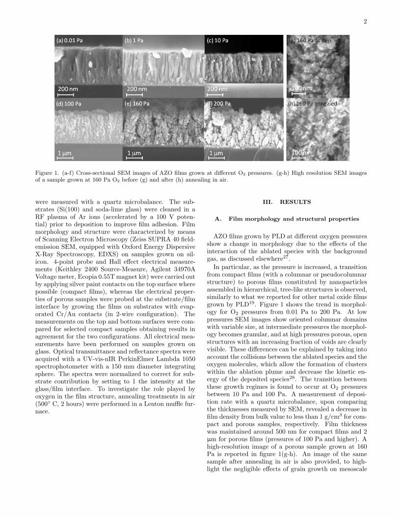
Figure 1. (a-f) Cross-sectional SEM images of AZO films grown at different O2 pressures. (g-h) High resolution SEM imagesof a sample grown at 160 Pa O2 before (g) and after (h) annealing in air.
were measured with a quartz microbalance. The sub-strates (Si(100) and soda-lime glass) were cleaned in aRF plasma of Ar ions (accelerated by a 100 V poten-tial) prior to deposition to improve film adhesion. Filmmorphology and structure were characterized by meansof Scanning Electron Microscopy (Zeiss SUPRA 40 field-emission SEM, equipped with Oxford Energy DispersiveX-Ray Spectroscopy, EDXS) on samples grown on sil-icon. 4-point probe and Hall effect electrical measure-ments (Keithley 2400 Source-Measure, Agilent 34970AVoltage meter, Ecopia 0.55T magnet kit) were carried outby applying silver paint contacts on the top surface wherepossible (compact films), whereas the electrical proper-ties of porous samples were probed at the substrate/filminterface by growing the films on substrates with evap-orated Cr/Au contacts (in 2-wire configuration). Themeasurements on the top and bottom surfaces were com-pared for selected compact samples obtaining results inagreement for the two configurations. All electrical mea-surements have been performed on samples grown onglass. Optical transmittance and reflectance spectra wereacquired with a UV-vis-nIR PerkinElmer Lambda 1050spectrophotometer with a 150 mm diameter integratingsphere. The spectra were normalized to correct for sub-strate contribution by setting to 1 the intensity at theglass/film interface. To investigate the role played byoxygen in the film structure, annealing treatments in air(500 C, 2 hours) were performed in a Lenton muffle fur-nace.
III. RESULTS
A. Film morphology and structural properties
AZO films grown by PLD at different oxygen pressuresshow a change in morphology due to the effects of theinteraction of the ablated species with the backgroundgas, as discussed elsewhere27.
In particular, as the pressure is increased, a transitionfrom compact films (with a columnar or pseudocolumnarstructure) to porous films constituted by nanoparticlesassembled in hierarchical, tree-like structures is observed,similarly to what we reported for other metal oxide filmsgrown by PLD19. Figure 1 shows the trend in morphol-ogy for O2 pressures from 0.01 Pa to 200 Pa. At lowpressures SEM images show oriented columnar domainswith variable size, at intermediate pressures the morphol-ogy becomes granular, and at high pressures porous, openstructures with an increasing fraction of voids are clearlyvisible. These differences can be explained by taking intoaccount the collisions between the ablated species and theoxygen molecules, which allow the formation of clusterswithin the ablation plume and decrease the kinetic en-ergy of the deposited species28. The transition betweenthese growth regimes is found to occur at O2 pressuresbetween 10 Pa and 100 Pa. A measurement of deposi-tion rate with a quartz microbalance, upon comparingthe thicknesses measured by SEM, revealed a decrease infilm density from bulk value to less than 1 g/cm3 for com-pact and porous samples, respectively. Film thicknesswas maintained around 500 nm for compact films and 2µm for porous films (pressures of 100 Pa and higher). Ahigh-resolution image of a porous sample grown at 160Pa is reported in figure 1(g-h). An image of the samesample after annealing in air is also provided, to high-light the negligible effects of grain growth on mesoscale
3
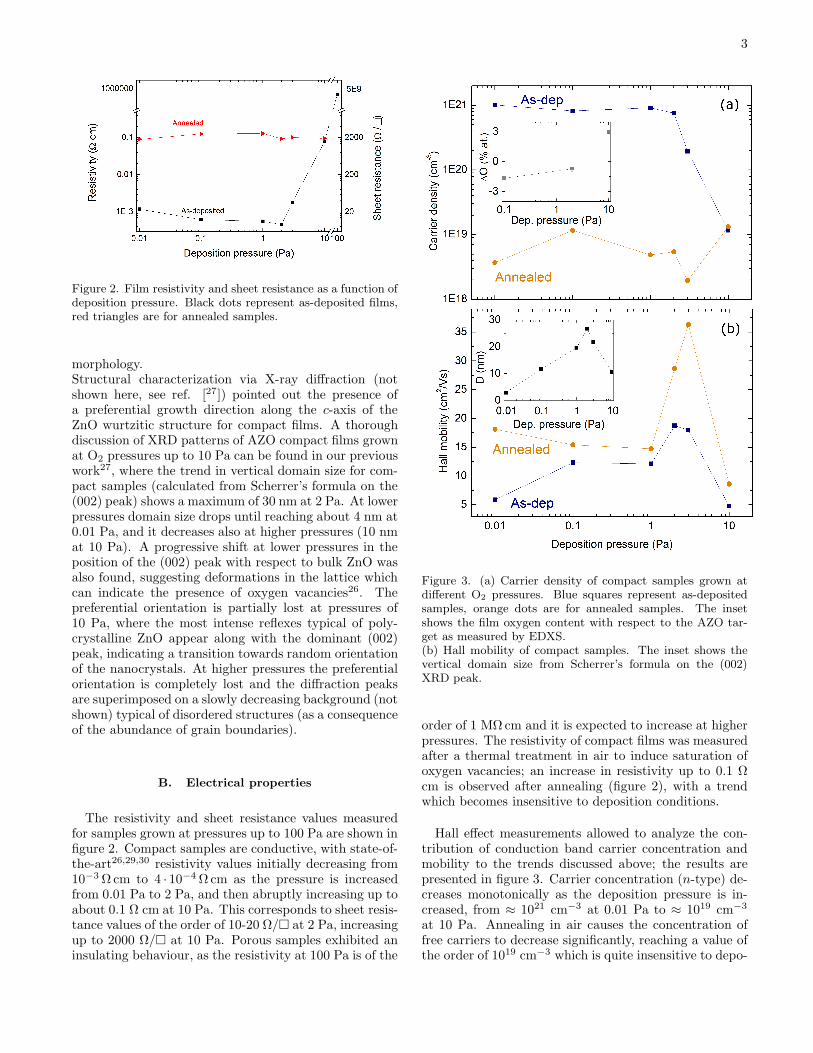
Figure 2. Film resistivity and sheet resistance as a function ofdeposition pressure. Black dots represent as-deposited films,red triangles are for annealed samples.
morphology.Structural characterization via X-ray diffraction (notshown here, see ref. [27]) pointed out the presence ofa preferential growth direction along the c-axis of theZnO wurtzitic structure for compact films. A thoroughdiscussion of XRD patterns of AZO compact films grownat O2 pressures up to 10 Pa can be found in our previouswork27, where the trend in vertical domain size for com-pact samples (calculated from Scherrer’s formula on the(002) peak) shows a maximum of 30 nm at 2 Pa. At lowerpressures domain size drops until reaching about 4 nm at0.01 Pa, and it decreases also at higher pressures (10 nmat 10 Pa). A progressive shift at lower pressures in theposition of the (002) peak with respect to bulk ZnO wasalso found, suggesting deformations in the lattice whichcan indicate the presence of oxygen vacancies26. Thepreferential orientation is partially lost at pressures of10 Pa, where the most intense reflexes typical of poly-crystalline ZnO appear along with the dominant (002)peak, indicating a transition towards random orientationof the nanocrystals. At higher pressures the preferentialorientation is completely lost and the diffraction peaksare superimposed on a slowly decreasing background (notshown) typical of disordered structures (as a consequenceof the abundance of grain boundaries).
B. Electrical properties
The resistivity and sheet resistance values measuredfor samples grown at pressures up to 100 Pa are shown infigure 2. Compact samples are conductive, with state-of-the-art26,29,30 resistivity values initially decreasing from10−3Ωcm to 4 · 10−4Ωcm as the pressure is increasedfrom 0.01 Pa to 2 Pa, and then abruptly increasing up toabout 0.1 Ω cm at 10 Pa. This corresponds to sheet resis-tance values of the order of 10-20 Ω/ at 2 Pa, increasingup to 2000 Ω/ at 10 Pa. Porous samples exhibited aninsulating behaviour, as the resistivity at 100 Pa is of the
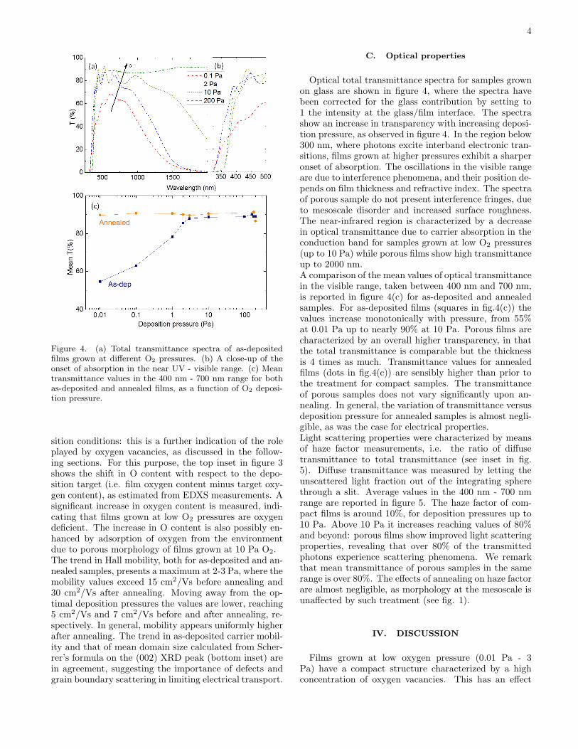
Figure 3. (a) Carrier density of compact samples grown atdifferent O2 pressures. Blue squares represent as-depositedsamples, orange dots are for annealed samples. The insetshows the film oxygen content with respect to the AZO tar-get as measured by EDXS.(b) Hall mobility of compact samples. The inset shows thevertical domain size from Scherrer’s formula on the (002)XRD peak.
order of 1 MΩcm and it is expected to increase at higherpressures. The resistivity of compact films was measuredafter a thermal treatment in air to induce saturation ofoxygen vacancies; an increase in resistivity up to 0.1 Ωcm is observed after annealing (figure 2), with a trendwhich becomes insensitive to deposition conditions.
Hall effect measurements allowed to analyze the con-tribution of conduction band carrier concentration andmobility to the trends discussed above; the results arepresented in figure 3. Carrier concentration (n-type) de-creases monotonically as the deposition pressure is in-creased, from ≈ 1021 cm−3 at 0.01 Pa to ≈ 1019 cm−3
at 10 Pa. Annealing in air causes the concentration offree carriers to decrease significantly, reaching a value ofthe order of 1019 cm−3 which is quite insensitive to depo-
4
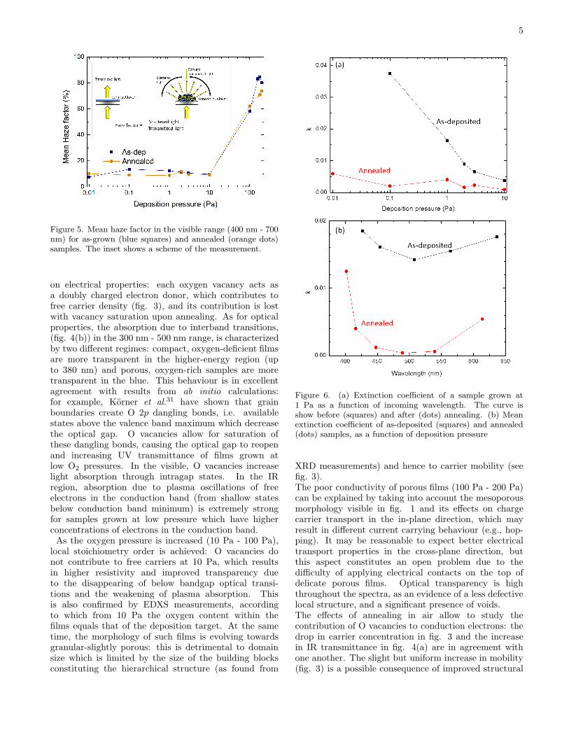
Figure 4. (a) Total transmittance spectra of as-depositedfilms grown at different O2 pressures. (b) A close-up of theonset of absorption in the near UV - visible range. (c) Meantransmittance values in the 400 nm - 700 nm range for bothas-deposited and annealed films, as a function of O2 deposi-tion pressure.
sition conditions: this is a further indication of the roleplayed by oxygen vacancies, as discussed in the follow-ing sections. For this purpose, the top inset in figure 3shows the shift in O content with respect to the depo-sition target (i.e. film oxygen content minus target oxy-gen content), as estimated from EDXS measurements. Asignificant increase in oxygen content is measured, indi-cating that films grown at low O2 pressures are oxygendeficient. The increase in O content is also possibly en-hanced by adsorption of oxygen from the environmentdue to porous morphology of films grown at 10 Pa O2.The trend in Hall mobility, both for as-deposited and an-nealed samples, presents a maximum at 2-3 Pa, where themobility values exceed 15 cm2/Vs before annealing and30 cm2/Vs after annealing. Moving away from the op-timal deposition pressures the values are lower, reaching5 cm2/Vs and 7 cm2/Vs before and after annealing, re-spectively. In general, mobility appears uniformly higherafter annealing. The trend in as-deposited carrier mobil-ity and that of mean domain size calculated from Scher-rer’s formula on the (002) XRD peak (bottom inset) arein agreement, suggesting the importance of defects andgrain boundary scattering in limiting electrical transport.
C. Optical properties
Optical total transmittance spectra for samples grownon glass are shown in figure 4, where the spectra havebeen corrected for the glass contribution by setting to1 the intensity at the glass/film interface. The spectrashow an increase in transparency with increasing deposi-tion pressure, as observed in figure 4. In the region below300 nm, where photons excite interband electronic tran-sitions, films grown at higher pressures exhibit a sharperonset of absorption. The oscillations in the visible rangeare due to interference phenomena, and their position de-pends on film thickness and refractive index. The spectraof porous sample do not present interference fringes, dueto mesoscale disorder and increased surface roughness.The near-infrared region is characterized by a decreasein optical transmittance due to carrier absorption in theconduction band for samples grown at low O2 pressures(up to 10 Pa) while porous films show high transmittanceup to 2000 nm.A comparison of the mean values of optical transmittancein the visible range, taken between 400 nm and 700 nm,is reported in figure 4(c) for as-deposited and annealedsamples. For as-deposited films (squares in fig.4(c)) thevalues increase monotonically with pressure, from 55%at 0.01 Pa up to nearly 90% at 10 Pa. Porous films arecharacterized by an overall higher transparency, in thatthe total transmittance is comparable but the thicknessis 4 times as much. Transmittance values for annealedfilms (dots in fig.4(c)) are sensibly higher than prior tothe treatment for compact samples. The transmittanceof porous samples does not vary significantly upon an-nealing. In general, the variation of transmittance versusdeposition pressure for annealed samples is almost negli-gible, as was the case for electrical properties.Light scattering properties were characterized by meansof haze factor measurements, i.e. the ratio of diffusetransmittance to total transmittance (see inset in fig.5). Diffuse transmittance was measured by letting theunscattered light fraction out of the integrating spherethrough a slit. Average values in the 400 nm - 700 nmrange are reported in figure 5. The haze factor of com-pact films is around 10%, for deposition pressures up to10 Pa. Above 10 Pa it increases reaching values of 80%and beyond: porous films show improved light scatteringproperties, revealing that over 80% of the transmittedphotons experience scattering phenomena. We remarkthat mean transmittance of porous samples in the samerange is over 80%. The effects of annealing on haze factorare almost negligible, as morphology at the mesoscale isunaffected by such treatment (see fig. 1).
IV. DISCUSSION
Films grown at low oxygen pressure (0.01 Pa - 3Pa) have a compact structure characterized by a highconcentration of oxygen vacancies. This has an effect
5
Figure 5. Mean haze factor in the visible range (400 nm - 700nm) for as-grown (blue squares) and annealed (orange dots)samples. The inset shows a scheme of the measurement.
on electrical properties: each oxygen vacancy acts asa doubly charged electron donor, which contributes tofree carrier density (fig. 3), and its contribution is lostwith vacancy saturation upon annealing. As for opticalproperties, the absorption due to interband transitions,(fig. 4(b)) in the 300 nm - 500 nm range, is characterizedby two different regimes: compact, oxygen-deficient filmsare more transparent in the higher-energy region (upto 380 nm) and porous, oxygen-rich samples are moretransparent in the blue. This behaviour is in excellentagreement with results from ab initio calculations:for example, Korner et al.
31 have shown that grainboundaries create O 2p dangling bonds, i.e. availablestates above the valence band maximum which decreasethe optical gap. O vacancies allow for saturation ofthese dangling bonds, causing the optical gap to reopenand increasing UV transmittance of films grown atlow O2 pressures. In the visible, O vacancies increaselight absorption through intragap states. In the IRregion, absorption due to plasma oscillations of freeelectrons in the conduction band (from shallow statesbelow conduction band minimum) is extremely strongfor samples grown at low pressure which have higherconcentrations of electrons in the conduction band.As the oxygen pressure is increased (10 Pa - 100 Pa),
local stoichiometry order is achieved: O vacancies donot contribute to free carriers at 10 Pa, which resultsin higher resistivity and improved transparency dueto the disappearing of below bandgap optical transi-tions and the weakening of plasma absorption. Thisis also confirmed by EDXS measurements, accordingto which from 10 Pa the oxygen content within thefilms equals that of the deposition target. At the sametime, the morphology of such films is evolving towardsgranular-slightly porous: this is detrimental to domainsize which is limited by the size of the building blocksconstituting the hierarchical structure (as found from
Figure 6. (a) Extinction coefficient of a sample grown at1 Pa as a function of incoming wavelength. The curve isshow before (squares) and after (dots) annealing. (b) Meanextinction coefficient of as-deposited (squares) and annealed(dots) samples, as a function of deposition pressure
XRD measurements) and hence to carrier mobility (seefig. 3).The poor conductivity of porous films (100 Pa - 200 Pa)can be explained by taking into account the mesoporousmorphology visible in fig. 1 and its effects on chargecarrier transport in the in-plane direction, which mayresult in different current carrying behaviour (e.g., hop-ping). It may be reasonable to expect better electricaltransport properties in the cross-plane direction, butthis aspect constitutes an open problem due to thedifficulty of applying electrical contacts on the top ofdelicate porous films. Optical transparency is highthroughout the spectra, as an evidence of a less defectivelocal structure, and a significant presence of voids.The effects of annealing in air allow to study thecontribution of O vacancies to conduction electrons: thedrop in carrier concentration in fig. 3 and the increasein IR transmittance in fig. 4(a) are in agreement withone another. The slight but uniform increase in mobility(fig. 3) is a possible consequence of improved structural
6
order upon annealing.The overall behaviour of electrical properties indicatesthat at low deposition pressure, O vacancies signifi-cantly contribute to conduction electron density, whosemobility is dictated by morphology and domain size athigher pressures. In this respect, several authors3,32
have pointed out how the adsorption of oxygen atomsat grain boundaries in AZO can cause the trapping ofcharge carriers and further decrease their mobility. Atany rate, it is reasonable to expect significant interplaybetween dopants and oxygen vacancies as far as con-cerns electrical properties; we are currently unable toinvestigate the position of Al3+ ions and O vacancies inthe lattice, and its effect on carrier concentration andmobility.The method of envelope analysis33,34 was employedto estimate the refractive index of compact films bynumerically solving the envelope equations for theposition of the interference fringes in transmittancespectra, knowing film thickness as measured by SEM.The results of our calculations indicate normal dispersionrelations for n (not shown), and the mean values of thereal part of the index in the visible range is found tobe about 1.90 for all compact films (pressures up to10 Pa), which is in agreement with the typical valuesfor ZnO (1.8-2.4)7. The variation of the extinctioncoefficient was also estimated over the visible spectrum(fig. 6(a)) and its mean value in the 400 nm - 700 nmrange as a function of deposition pressure is reportedin fig. 6(b). The calculated dispersion relations ofthe imaginary part k show a minimum in the visibleand a dependence on deposition pressure following thetrends found in transmittance: films grown at higheroxygen pressures are characterized by a higher degreeof structural order resulting in less significant lightabsorption. The extinction coefficient of samples grownat low pressures decreases by a factor 10 upon annealing,giving confirmation of the effect of defect healing ontransparency. It is also worthwile to notice that thereis qualitative agreement between this estimate of k andan estimate of the absorption coefficient α taken fromLambert-Beer’s law, as the relation α = 4πk/λ holds(substituting the average values yields α ≈ 104 cm−1).
The optical gap was measured by means of Taucplots35, by plotting (αhν)2 vs. hν in proximity of theonset of absorption, taking α from transmittance spectravia Lambert-Beer’s law (the relation α = − lnT/d, whered denotes film thickness, was used since reflectance wasnegligible in this spectral range) and performing a linearfit in the region where (αhν)2 ∝
√
hν − Eg, where Eg isthe optical gap. The intercept of the linear fit thus givesEg. The choice of using (αhν)2 in the plots is due to thedirect bandgap of ZnO and to the estimated filling of theconduction band, as discussed by Buchholz et al.36. Thebehaviour of Eg as a function of deposition pressure isreported in figure 7, where the inset shows an exampleof Tauc plot for a porous sample.
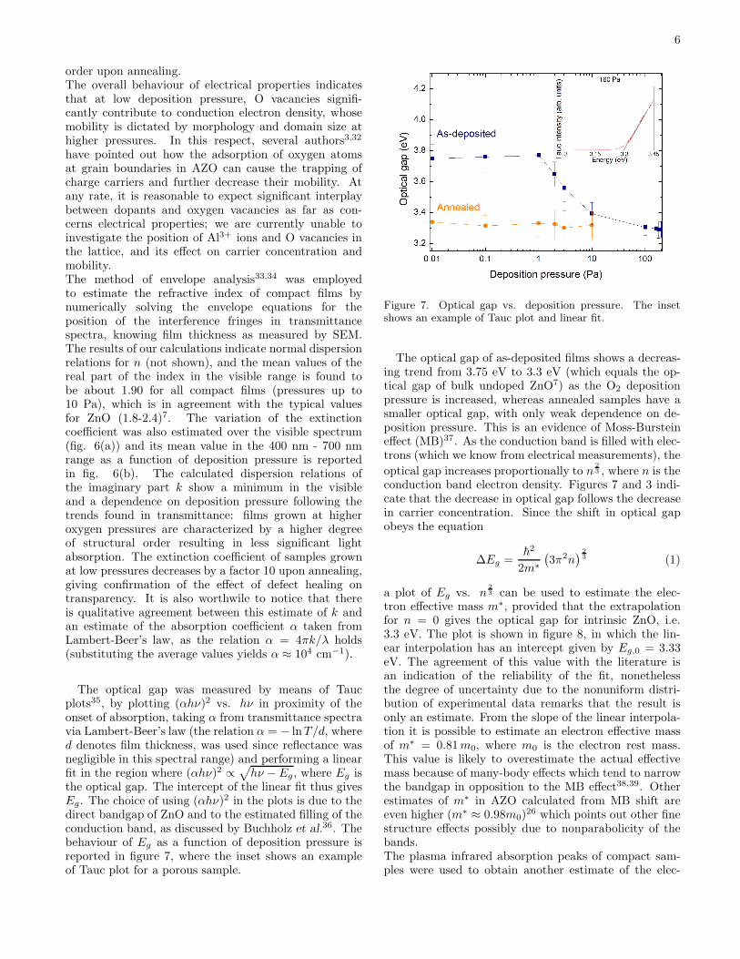
Figure 7. Optical gap vs. deposition pressure. The insetshows an example of Tauc plot and linear fit.
The optical gap of as-deposited films shows a decreas-ing trend from 3.75 eV to 3.3 eV (which equals the op-tical gap of bulk undoped ZnO7) as the O2 depositionpressure is increased, whereas annealed samples have asmaller optical gap, with only weak dependence on de-position pressure. This is an evidence of Moss-Bursteineffect (MB)37. As the conduction band is filled with elec-trons (which we know from electrical measurements), the
optical gap increases proportionally to n2
3 , where n is theconduction band electron density. Figures 7 and 3 indi-cate that the decrease in optical gap follows the decreasein carrier concentration. Since the shift in optical gapobeys the equation
∆Eg =~2
2m∗
(
3π2n)
2
3 (1)
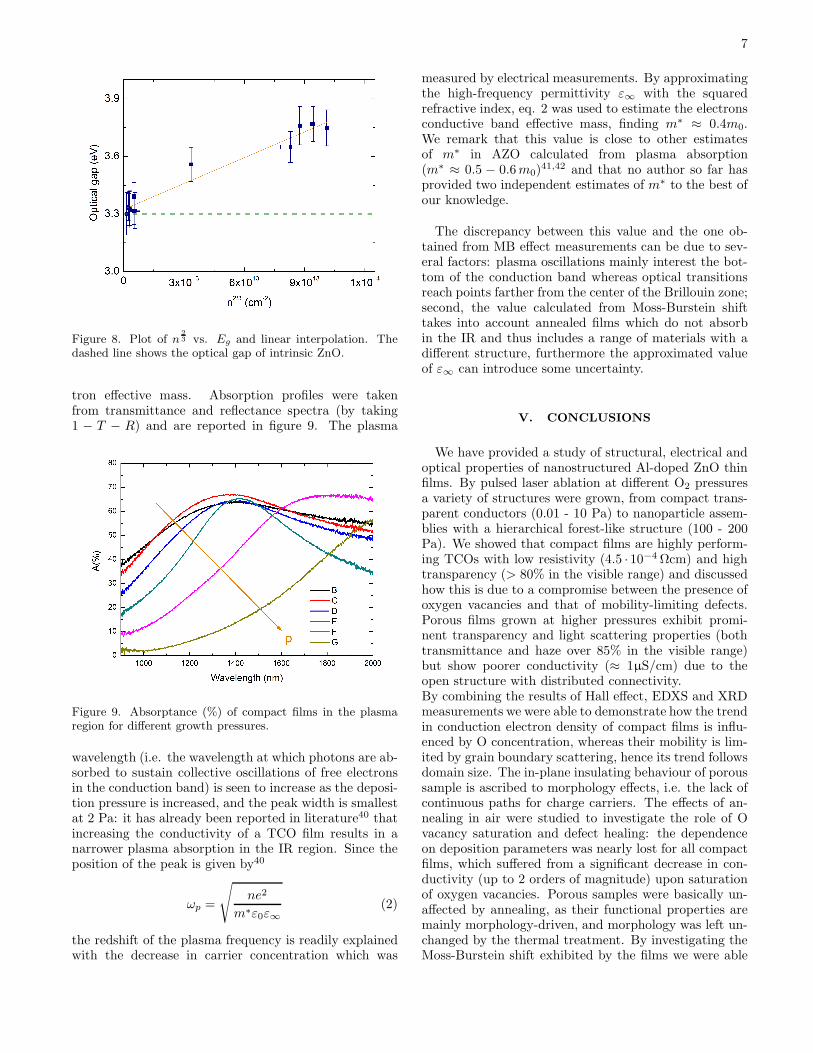
a plot of Eg vs. n2
3 can be used to estimate the elec-tron effective mass m∗, provided that the extrapolationfor n = 0 gives the optical gap for intrinsic ZnO, i.e.3.3 eV. The plot is shown in figure 8, in which the lin-ear interpolation has an intercept given by Eg,0 = 3.33eV. The agreement of this value with the literature isan indication of the reliability of the fit, nonethelessthe degree of uncertainty due to the nonuniform distri-bution of experimental data remarks that the result isonly an estimate. From the slope of the linear interpola-tion it is possible to estimate an electron effective massof m∗ = 0.81m0, where m0 is the electron rest mass.This value is likely to overestimate the actual effectivemass because of many-body effects which tend to narrowthe bandgap in opposition to the MB effect38,39. Otherestimates of m∗ in AZO calculated from MB shift areeven higher (m∗
≈ 0.98m0)26 which points out other fine
structure effects possibly due to nonparabolicity of thebands.The plasma infrared absorption peaks of compact sam-ples were used to obtain another estimate of the elec-
7
Figure 8. Plot of n2
3 vs. Eg and linear interpolation. Thedashed line shows the optical gap of intrinsic ZnO.
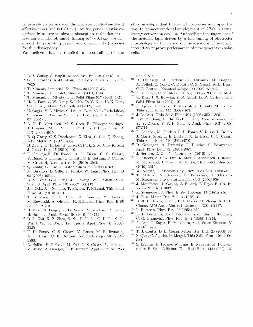
tron effective mass. Absorption profiles were takenfrom transmittance and reflectance spectra (by taking1 − T − R) and are reported in figure 9. The plasma
Figure 9. Absorptance (%) of compact films in the plasmaregion for different growth pressures.
wavelength (i.e. the wavelength at which photons are ab-sorbed to sustain collective oscillations of free electronsin the conduction band) is seen to increase as the deposi-tion pressure is increased, and the peak width is smallestat 2 Pa: it has already been reported in literature40 thatincreasing the conductivity of a TCO film results in anarrower plasma absorption in the IR region. Since theposition of the peak is given by40
ωp =
√
ne2
m∗ε0ε∞(2)
the redshift of the plasma frequency is readily explainedwith the decrease in carrier concentration which was
measured by electrical measurements. By approximatingthe high-frequency permittivity ε∞ with the squaredrefractive index, eq. 2 was used to estimate the electronsconductive band effective mass, finding m∗
≈ 0.4m0.We remark that this value is close to other estimatesof m∗ in AZO calculated from plasma absorption(m∗
≈ 0.5 − 0.6m0)41,42 and that no author so far has
provided two independent estimates of m∗ to the best ofour knowledge.
The discrepancy between this value and the one ob-tained from MB effect measurements can be due to sev-eral factors: plasma oscillations mainly interest the bot-tom of the conduction band whereas optical transitionsreach points farther from the center of the Brillouin zone;second, the value calculated from Moss-Burstein shifttakes into account annealed films which do not absorbin the IR and thus includes a range of materials with adifferent structure, furthermore the approximated valueof ε∞ can introduce some uncertainty.
V. CONCLUSIONS
We have provided a study of structural, electrical andoptical properties of nanostructured Al-doped ZnO thinfilms. By pulsed laser ablation at different O2 pressuresa variety of structures were grown, from compact trans-parent conductors (0.01 - 10 Pa) to nanoparticle assem-blies with a hierarchical forest-like structure (100 - 200Pa). We showed that compact films are highly perform-ing TCOs with low resistivity (4.5 · 10−4Ωcm) and hightransparency (> 80% in the visible range) and discussedhow this is due to a compromise between the presence ofoxygen vacancies and that of mobility-limiting defects.Porous films grown at higher pressures exhibit promi-nent transparency and light scattering properties (bothtransmittance and haze over 85% in the visible range)but show poorer conductivity (≈ 1µS/cm) due to theopen structure with distributed connectivity.By combining the results of Hall effect, EDXS and XRDmeasurements we were able to demonstrate how the trendin conduction electron density of compact films is influ-enced by O concentration, whereas their mobility is lim-ited by grain boundary scattering, hence its trend followsdomain size. The in-plane insulating behaviour of poroussample is ascribed to morphology effects, i.e. the lack ofcontinuous paths for charge carriers. The effects of an-nealing in air were studied to investigate the role of Ovacancy saturation and defect healing: the dependenceon deposition parameters was nearly lost for all compactfilms, which suffered from a significant decrease in con-ductivity (up to 2 orders of magnitude) upon saturationof oxygen vacancies. Porous samples were basically un-affected by annealing, as their functional properties aremainly morphology-driven, and morphology was left un-changed by the thermal treatment. By investigating theMoss-Burstein shift exhibited by the films we were able
8
to provide an estimate of the electron conduction bandeffective mass (m∗
≈ 0.81m0). An indipendent estimatederived from carrier infrared absorption and index of re-fraction was also obtained, finding m∗
≈ 0.4m0: we dis-cussed the possible (physical and experimental) reasonsfor this discrepancy.We believe that a detailed understanding of the
structure-dependent functional properties may open theway to non-conventional employment of AZO in actualenergy conversion devices. An intelligent management ofthe incident light driven by a fine tuning of electrodesmorphology at the nano- and mesoscale is of potentialinterest to improve performance of new generation solarcells.
1 D. S. Ginley, C. Bright, Mater. Res. Bull. 25 (2000) 15.2 G. J. Exarhos, X.-D. Zhou, Thin Solid Films 515 (2007)7025.
3 T. Minami, Semicond. Sci. Tech. 20 (2005) 35.4 T. Minami, Thin Solid Films 516 (2008) 1314.5 T. Minami, T. Miyata, Thin Solid Films 517 (2008) 1474.6 H.-K. Park, J.-W. Kang, S.-I. Na, D.-Y. Kim, H.-K. Kim,Sol. Energy Mater. Sol. Cells 93 (2009) 1994.
7 U. Ozgur, Y. I. Alivov, C. Liu, A. Teke, M. A. Reshchikov,S. Dogan, V. Avrutin, S.-J. Cho, H. Morcoc, J. Appl. Phys.98 (2005) 1.
8 A. B. F. Martinson, M. S. Goes, F. Fabregat-Santiago,J. Bisquert, M. J. Pellin, J. T. Hupp, J. Phys. Chem. A113 (2009) 4015.
9 B. Q. Zhang, C. S. Dandeneau, X. Zhou, G. Cao, Q. Zhang,Adv. Mater. 21 (2009) 4087.
10 B. Zhang, D.-H. Lee, H. Chae, C. Park, S. M. Cho, KoreanJ. Chem. Eng. 27 (2010) 999.
11 F. Sauvage,F. Di Fonzo, A. Li Bassi, C. S. Casari,V. Russo, G. Divitini, C. Ducati, C. E. Bottani, P. Comte,M. Graetzel, Nano Letters 10 (2010) 2562.
12 Q. Zhang, G. Cao, J. Mater. Chem. 21 (2011) 6769.13 M. Birkholz, B. Selle, F. Fenske, W. Fuhs, Phys. Rev. B
68 (2003) 205414.14 B.-Z. Dong, G.-J. Fang, J.-F. Wang, W.-J. Guan, X.-Z.
Zhao, J. Appl. Phys. 101 (2007) 033713.15 J.-i. Oda, J.-i. Nomoto, T. Miyata, T. Minami, Thin Solid
Films 518 (2010) 2984.16 T. Makino, C. H. Chia, K. Tamura, Y. Segawa,
M. Kawasaki, A. Ohtomo, H. Koinuma, Phys. Rev. B 65(2002) 121201.
17 B. Nasr, S. Dasgupta, D. Wang, N. Mechau, R. Kruk,H. Hahn, J. Appl. Phys. 108 (2010) 103721.
18 B. L. Zhu, X. Z. Zhao, S. Xu, F. H. Su, G. H. Li, X. G.Wu, J. Wu, R. Wu, J. Liu, Jpn. J. Appl. Phys. 47 (2008)2225.
19 F. Di Fonzo, C. S. Casari, V. Russo, M. F. Brunella,A. Li Bassi, C. E. Bottani, Nanotechnology 20 (2009)15604.
20 A. Bailini, F. DiFonzo, M. Fusi, C. S. Casari, A. Li Bassi,V. Russo, A. Baserga, C. E. Bottani, Appl. Surf. Sci. 253
(2007) 8130.21 D. Dellasega, A. Facibeni, F. DiFonzo, M. Bogana,
A. Polissi, C. Conti, C. Ducati, C. S. Casari, A. Li Bassi,C. E. Bottani, Nanotechnology 19 (2008) 475602.
22 A. V. Singh, R. M. Mehra, J. Appl. Phys. 90 (2001) 5661.23 H. Kim, J. S. Horwitz, S. B. Qadri, D. B. Chrisey, Thin
Solid Films 421 (2002) 107.24 H. Agura, A. Suzuki, T. Matsushita, T. Aoki, M. Okuda,
Thin Solid Films 445 (2003) 263.25 J. Lackner, Thin Solid Films 494 (2006) 302 – 306.26 B.-Z. Z. Dong, H. Hu, G.-J. J. Fang, X.-Z. Z. Zhao, D.-
Y. Y. Zheng, Y.-P. P. Sun, J. Appl. Phys. 103 (2008)073711.
27 P. Gondoni, M. Ghidelli, F. Di Fonzo, V. Russo, P. Bruno,J. Martı-Rujas, C. E. Bottani, A. Li Bassi, C. S. Casari,Thin Solid Films 520 (2012)4707.
28 D. Geohegan, A. Puretzky, G. Duscher, S. Pennycook,Appl. Phys. Lett. 72 (1998) 2987.
29 J. Herrero, C. Guillen, Vacuum 84 (2010) 924.30 A. Anders, S. H. N. Lim, K. Man, J. Andersson, J. Rosen,
M. Mcfarland, J. Brown, K. M. Yu, Thin Solid Films 518(2010) 3313.
31 W. Korner, C. Elsasser, Phys. Rev. B 81 (2010) 085324.32 T. Makino, Y. Segawa, A. Tsukazaki, A. Ohtomo,
M. Kawasaki, Phys. Status Solidi C, 3 (2006) 95633 J. Manifacier, J. Gasiot, J. Fillard, J. Phys. E: Sci. In-
strum. 9 (1976) 1002.34 R. Swanepoel, J. Phys. E: Sci. Instrum. 17 (1984) 896.35 J. Tauc, Mater. Res. Bull. 3 (1968) 37.36 D. B. Buchholz, J. Liu, T. J. Marks, M. Zhang, R. P. H.
Chang, ACS Appl. Mater. Interfaces 1 (2009) 2147.37 L. Burstein, Phys. Rev. 93 (1954) 632.38 B. E. Sernelius, K.-F. Berggren, Z.-C. Jin, I. Hamberg,
C. G. Granqvist, Phys. Rev. B 37 (1988) 10244.39 A. Jain, P. Sagar, R. M. Mehra, Solid-State Electron. 50
(2006) 1420.40 T. J. Coutts, D. L. Young, Mater. Res. Bull. 25 (2000) 58.41 Z. Qiao, C. Agashe, D. Mergel, Thin Solid Films 496 (2006)
520.42 S. Brehme, F. Fenske, W. Fuhs, E. Nebauer, M. Poschen-
rieder, B. Selle, I. Sieber, Thin Solid Films 342 (1999) 167.