Selective light absorber-assisted single nickel atom catalysts ...
Upload
independentCategory
view
0download
0
Energy Procedia 10 (2011) 122 – 127
1876-6102 © 2011 Published by Elsevier Ltd. Selection and/or peer-review under responsibility of Organizers of European Materials Research Society (EMRS) Conference: Symposium on Advanced Inorganic Materials and Concepts for Photovoltaics.doi:10.1016/j.egypro.2011.10.164
Available online at www.sciencedirect.com
Available online at www.sciencedirect.com
Energy Procedia 00 (2011) 000–000
www.elsevier.com/locate/procedia
European Materials Research Society Conference Symp. Advanced Inorganic Materials and Concepts for Photovoltaics
ZnO/CdTe and ZnO/CdS coreshell nanowire arrays for
extremely thin absorber solar cells
Raúl Salazara*, Alexandru Delamoreanub, Claude LévyClémentc, Valentina Ivanovaa*
In this study we report on ZnO/CdTe coreshell nanostructures fabrication for extremely thin absorber (Eta)solar cells. Successive ion layer adsorption and reaction (SILAR) and close space sublimation (CSS) methods were used to sensitize electrodeposited ZnO nanowires by CdS and CdTe. The close morphological investigation showed that CdTe thin layer deposited by CSS method did not uniformly cover the ZnO nanowires (NWs). On the tip of the NWs, nanoparticles with a 20 nm diameter were observed whereas some areas were not covered, which could affect the solar cell efficiency. ZnO/CdS nanowires arrays were prepared by SILAR technique and were compared to those of ZnO/CdTe. The obtained uniform layers (~ 25 nm thick) on the entire ZnO NWs surface allowed us to consider SILAR method as a good alternative for deposition of conformal extremely thin films. The adsorption edge up to 800 nm for CdTe compared to 500 nm for CdS, foresees the ZnO/CdTe core/shell structure favourable to achieve good photovoltaic performances. Enhanced optical properties of the nanostuctured electrodes over the planar counterparts proved the effect of the increased surface area. © 2010 Published by Elsevier Ltd. Selection and/or peerreview under responsibility of the symposium organizers: G. Conibeer; Yongxiang Li; j. Poortmans; M. Kondo; A. Slaoui; M. Tao; M. Topic sore/shell nanostructures; type II band alignment; etasolar cell; solar energy conversion.
* Corresponding authors: Tel.: +33438786504; fax: +33438783034. : [email protected]; [email protected]
© 2011 Published by Elsevier Ltd. Selection and/or peer-review under responsibility of Organizers of European Materials Research Society (EMRS) Conference: Symposium on Advanced Inorganic Materials and Concepts for Photovoltaics.
Raúl Salazar et al. / Energy Procedia 10 (2011) 122 – 127 1232
Highly efficient and low cost solar cells remain among the potential choices to solve climate problems and meet the increasing demand of global energy. Research on the socalled “nextgeneration” solar cells is focused in the development of costeffective clean sources of energy. Dye sensitized [1], organic, and semiconductor sensitized solar cells are among the most investigated architectures. In spite of the obtained encouraging results, there are still numerous hurdles like the lack of long term stability of organic and dye–sensitized solar cells [2], the ineffective loading of dyes or quantum dots (QDs) as sensitizers [3, 4], the carrier losses by nonradiative recombination processes [5], the ineffective band alignment between materials [6], … etc that need to be solved in order to produce highly efficient, stable and cheap solar devices.
The nanowires based solar cell is a configuration permitting to address many of the above mentioned problems. The increased surface area developed by the nanostructured electrode offers the possibility to reduce the required thickness of the absorbing material in comparison with thin film solar cells due to light trapping and scattering effects [7, 8]. The onedimensional structure of nanowires serves as direct pathway for the transport of carriers and efficiencies have been increased compared to the nanoparticles or the porous versions [9, 10]. It is also expected that an allinorganic solar cell represents a potentiallylonglasting stable device.
In general, the extremely thin absorber (Eta)solar cell consists of an extremely thin absorbing layer (Eg ~ 1.11.8 eV) embedded between n and ptype nanostructured electrodes (Eg > 3 eV). Due to the extremely small thickness of the absorber (few tens of nanometers), photogenerated charges are separated by the electric field of the pn junction before they recombine [11]. The Etasolar cell based on the ZnO/CdTe coreshell nanowire array appears to be a viable solution due to the high electron mobility of ZnO and the remarkable optical properties of CdTe as semiconductor sensitizer: high absorption coefficient (> 104 cm1) and a band gap (1.5 eV) matching the solar radiation spectrum [12]. Different deposition techniques like: Chemical Bath Deposition (CBD), electrodeposition, QD funtionalization, Close Space Sublimation (CSS), successive ion layer adsorption and reaction (SILAR), Metal Organic Chemical Vapor Deposition (MOCVD), vapour phase epitaxy (VPE), etc…, have been used to conformally deposit the absorber layer onto different types of nanostructures. TiO2 and ZnO nanostructures have been successfully sensitized with semiconductor QD and thin layers of CdSe [13], PbSe [14], CuInS2 [15], CuInSe2 [16], CdS [1719], CdSSe [20], ZnTe [21], ZnSe [22] and CdTe [11,23,24]. Although promising results have been obtained in the last years, the solar cell efficiency suffered from high carrier recombination and/or resistive losses in the absorber due to low quality of the materials and defective interfaces in the heterojunction.
Here we report on ZnO/CdS and ZnO/CdTe core/shell nanowires prepared for Etasolar cells. SILAR and CSS methods were used to sensitize electrodeposited ZnO nanowires by CdS and CdTe. The structural and optical properties for different shell thicknesses of ZnO/CdS and ZnO/CdTe core/shell nanostructures were analyzed.
A 200 nmthick 2D ZnO buffer layer was electrodeposited with a 0.4 C cm2 charge density at 50°C on transparent conducting oxide (TCO) SnO2:F/glass, (AGC Fabritech Co., Ltd. Japan 10/□). The obtained thin film was used for the subsequent electrochemical deposition of the ZnO nanowire arrays with a 10 C cm2 charge density at temperature of 80°C [25]. The chemicals (ZnCl2 and KCl) were ALDRICH analytical reagent grade.
124 Raúl Salazar et al. / Energy Procedia 10 (2011) 122 – 127 3
A thin layer of CdTe was subsequently deposited on ZnO NWs by CSS. The CdTe source and substrate temperatures were 580 and 480°C, respectively. Deposition times were 3.5 and 7 min. The amount of deposited CdTe for 7 min was 3.8 x 10⁴ gms.
The CdS shell of the ZnO/CdS nanowires was realized by the SILAR method. Sodium sulfide nonahydrate (SIGMAALDRICH Na2S9H2O ACS reagent ≥ 98%) and cadmium nitrate tetrahydrate (ACROS organics CdN2O64H2O) were used to prepare 50 mM Cd2+ cationic and S2 anionic source solutions. A complete SILAR deposition cycle consisted of successive dippings of the ZnO nanowires in the Cd2+ and in the S2 ionic solutions for 20 seconds. After each immersion the samples were rinsed with deionized water also for 20 seconds. Thickness, structural and optical properties were controlled by the number of deposition cycles [26].
The structural properties of bare ZnO, ZnO/CdTe, and ZnO/CdS NWs were studied by scanning electron microscopy (SEM), Zeiss ULTRA 55. Xray diffraction data were recorded on a Panalytical X’Pert MPD Xray diffractometer using the CoKα radiation 1.7889 Å wavelength. The optical absorbance spectra (3001200 nm) were measured at room temperature with a Hitachi UVVISNIR 4001 spectrophotometer fitted with an integrating sphere.
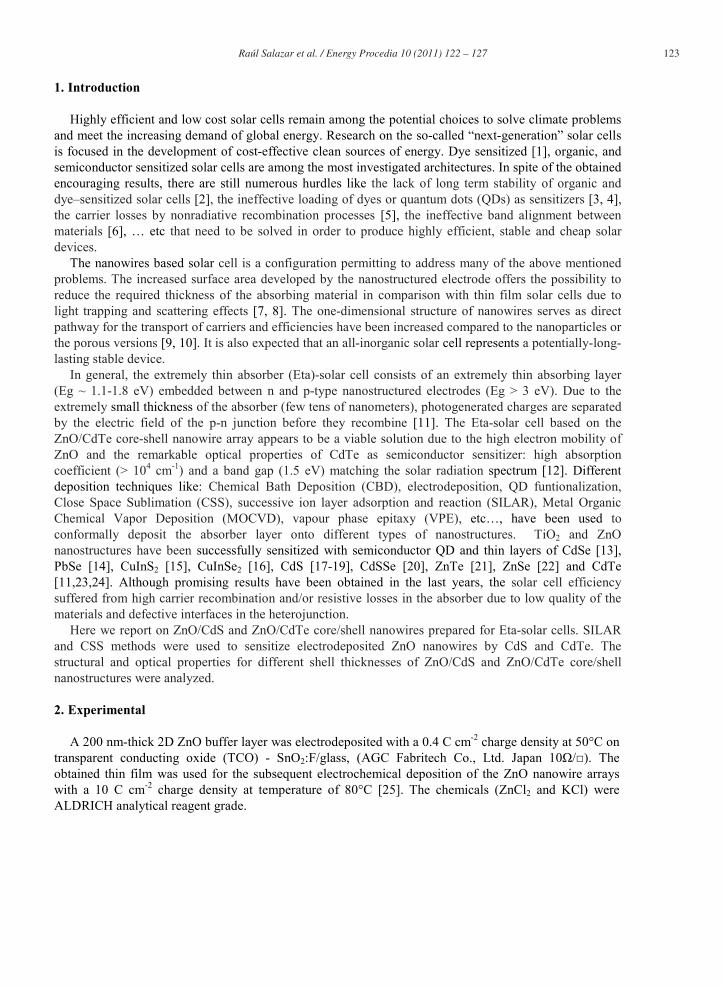
SEM image of electrodeposited ZnO NWs with length about 1.5 m and diameter around 150 nm which were consequently used as the core part of the structure is shown in Fig. 1a. They are slightly tilted, as a result of the randomly oriented ZnO small grains in the 2D layer, but in overall they are oriented perpendicular to the TCO substrate. In Figs. 1b and 1c are depicted the corresponding ZnO/CdTe core/shell nanowires. Fig. 1b shows the surface morphology when a shorter deposition time (3.5 min) was applied. It is seen that the NWs surface is not completely covered and it was difficult to estimate the layer thickness. The layer was composed of CdTe pyramidlike nanoparticles (see the inset in Fig. 1b). It has been already reported in the literature that in the case of CdTe deposition by CSS, the considerably large growth rate is driven by surface minimization due to the thermodynamic factors influence [27]. Longer deposition time (7 min) produced ZnO NWs well lined with CdTe (Fig. 1c). The CdTe shell thickness was estimated to be > 30 nm from STEM images. The shell seems to be formed by 20 nm nanoparticles (average size), mostly aggregated at the nanowire tips. This not uniform shell layer evidences the need of optimization of ZnO nanowire length in order to avoid the shadowing effects.
With the aim to find suitable deposition method for preparation of a more conformal shell layer around the ZnO nanowire core, and to explore other sensitizing materials, solutionbased SILAR deposition of CdS was carried out. Fig. 1d shows the ZnO/CdS core/shell nanostructures after 40 cycles of SILAR deposition. From the SEM image we can figure that the shell layer is formed by loosely packed CdS particles, which seem to be mostly accumulated at nanowire tips. But the STEM analysis has confirmed the CdS formation on the entire nanowire surface and only slight nanoparticle aggregations on the top. The estimated thickness of CdS film is about 25 nm (Fig. 1e).
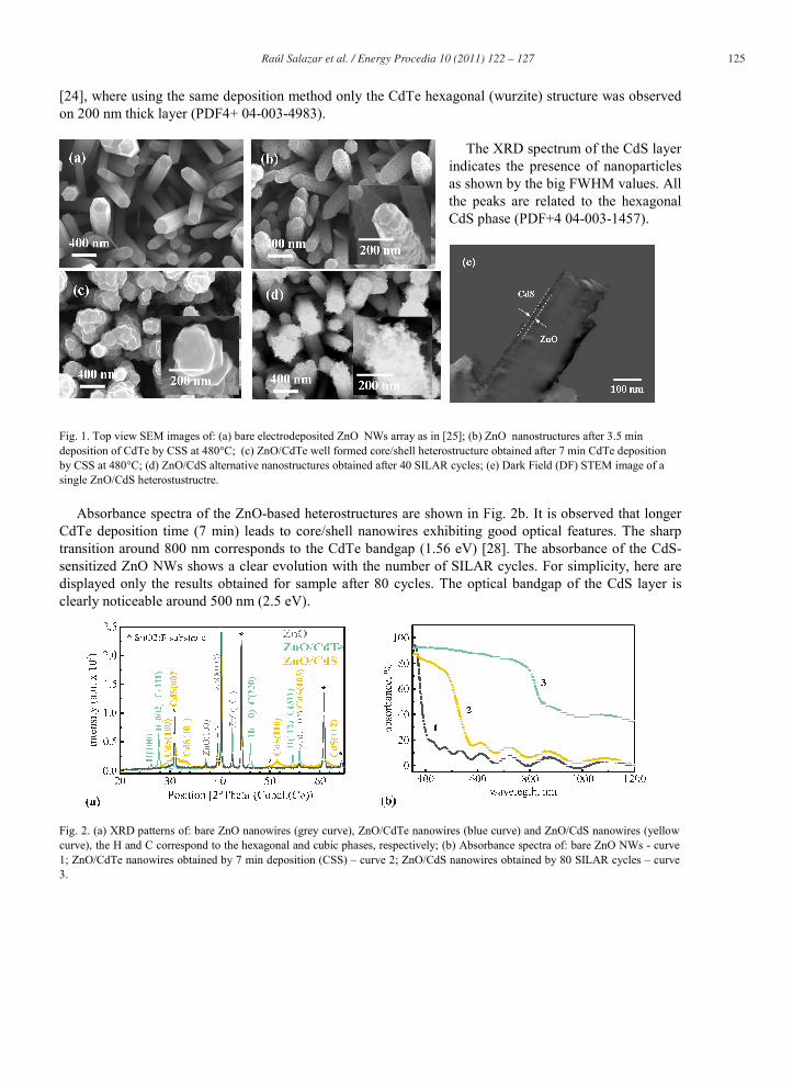
The XRD spectrum of the bare ZnO NWs (Fig. 2a) demonstrates the preferential growth along the <0001>direction and less intense diffraction peaks confirm the ZnO hexagonal (wurtzite) structure, in agreement with data (PDF4+ 040045134).
Diffraction peaks belonging to CdTe were detected on the XRD spectrum of the ZnO/CdTe sample. Small Full Width at Half Maximum (FWHM) values of the peaks from CdTe demonstrate the material high crystalline quality and large grain size obtained by CSS. Due to the discrepancies in the relative intensities of the diffraction peaks, the CdTe layer could be considered as a mixture of hexagonal and cubic (zinblend) phases (PDF4+ 040035711) (Fig. 2a). Contrary to the results have been reported in ref
Raúl Salazar et al. / Energy Procedia 10 (2011) 122 – 127 1254
[24], where using the same deposition method only the CdTe hexagonal (wurzite) structure was observed on 200 nm thick layer (PDF4+ 040034983).
The XRD spectrum of the CdS layer
indicates the presence of nanoparticles as shown by the big FWHM values. All the peaks are related to the hexagonal CdS phase (PDF+4 040031457).
Fig. 1. Top view SEM images of: (a) bare electrodeposited ZnO NWs array as in [25]; (b) ZnO nanostructures after 3.5 min deposition of CdTe by CSS at 480°C; (c) ZnO/CdTe well formed core/shell heterostructure obtained after 7 min CdTe deposition by CSS at 480°C; (d) ZnO/CdS alternative nanostructures obtained after 40 SILAR cycles; (e) Dark Field (DF) STEM image of a single ZnO/CdS heterostustructre.
Absorbance spectra of the ZnObased heterostructures are shown in Fig. 2b. It is observed that longer CdTe deposition time (7 min) leads to core/shell nanowires exhibiting good optical features. The sharp transition around 800 nm corresponds to the CdTe bandgap (1.56 eV) [28]. The absorbance of the CdSsensitized ZnO NWs shows a clear evolution with the number of SILAR cycles. For simplicity, here are displayed only the results obtained for sample after 80 cycles. The optical bandgap of the CdS layer is clearly noticeable around 500 nm (2.5 eV).
Fig. 2. (a) XRD patterns of: bare ZnO nanowires (grey curve), ZnO/CdTe nanowires (blue curve) and ZnO/CdS nanowires (yellow curve), the H and C correspond to the hexagonal and cubic phases, respectively; (b) Absorbance spectra of: bare ZnO NWs curve 1; ZnO/CdTe nanowires obtained by 7 min deposition (CSS) – curve 2; ZnO/CdS nanowires obtained by 80 SILAR cycles – curve 3.
126 Raúl Salazar et al. / Energy Procedia 10 (2011) 122 – 127 5
We have shown that it is possible to sensitize the electrodeposited ZnO nanowires with CdTe and CdS thin films. The properties of the obtained core/shell nanowires have been analyzed with the purpose to use them Etasolar cell. The quality of the layers obtained by CSS and SILAR deposition methods has been compared. The resulted layer thicknesses were about 40 nm for CdTe and 25 nm for CdS using CSS and SILAR, respectively. An aggregation at the NWs tip was observed for both techniques, however to a lesser extend for the SILAR method. It could hinder the interpenetration of other solar cell components and therefore affect the device efficiency. The SILAR technique seems to be a promising method to synthesize thin layers with easily controlled thickness.
This work has been financially supported by the Nanosciences Foundation of Grenoble. The authors gratefully acknowledge the support from CONACYT Mexico, Dr Peter Reiss (CEAINAC) for giving us access to chemistry laboratory, Muriel Jolliot (CEALETI) for CdTe preparation by CSS. Xray diffraction analysis was done at CEAINAC/SP2M/SGX, Grenoble, France.
[1] O'Regan B, Grätzel M. A lowcost, highefficiency solar cell based on dyesensitized colloidal TiO2 films. 1991;(6346):737–740.
[2] Kato N, Takeda Y, Higuchi K, Takeichi A, Sudo E, Tanaka H et al. Degradation analysis of dyesensitized solar cell module after longterm stability test under outdoor working condition. 2009;:893–7.
[3] Chou TP, Zhang Q, Cao G.Effects of Dye Loading Conditions on the Energy Conversion Efficiency of ZnO and TiO2 DyeSensitized Solar Cells. 2007;:1880418811.
[4] Lokteva I, Radychev N, Witt F, Borchert H, Parisi J, KolnyOlesiak J. Surface Treatment of CdSe Nanoparticles for Application in Hybrid Solar Cells: The Effect of Multiple Ligand Exchange with Pyridine. 2010;:1278412791.
[5] Boix PP, Ajuria J, Pacios R, GarciaBelmonte G. Carrier recombination losses in inverted polymer: Fullerene solar cells with ZnO holeblocking layer from transient photovoltage and impedance spectroscopy techniques. 2011;:0745141.
[6] Yip HL, Hau SK, Baek NS, Ma H, Alex K, Y Jen. Polymer Solar Cells That Use SelfAssembledMonolayerModified ZnO/Metals as Cathodes. 2008;:2376–2382.
[7] LévyClément C, TenaZaera R, Ryan MA, Abou K, Hodes G. CdSeSensitized pCuSCN/Nanowire nZnO Heterojuntions. 2005 ;:15121515.
[8] Möller J, Fischer CHH, Siebentritt S, Könenkamp R, LuxSteiner MCh. CuInS2 as an extremely thin absorber in an eta solar cell. In: Schmid J. [u.a.] [Eds.]: ,European Commission, Luxemburg; 1998, p. 209211.
[9] Ernst K, Engelhardt R, Ellmer K, Kelch C, Muffler HJ, LuxSteiner MCh, Könenkamp R. Contacts to a solar cell with extremely thin CdTe absorber. 2001;:2628.
[10] Zhang Q, Cao G. Nanostructured photoelectrodes for dyesensitized solar cells. 2011;91109. [11] LévyClément C. Nanostructured ETASolar Cells. In: Tetsuo Soga, editor.
, Amsterdam: Elsevier B.V; 2007, p. 447484. [12] LévyClément C, Katty A, Bastide S, Zenia F, Mora I, MunozSanjose V. A new CdTe/ZnO columnar composite film for
Etasolar cells. 2002;:229232.
Raúl Salazar et al. / Energy Procedia 10 (2011) 122 – 127 1276
[13] Leschkies KS, Divakar R, Basu J, EnachePommer E, Boercker JE, Carter CB et al. Photosensitization of ZnO Nanowires with CdSe Quantum Dots for Photovoltaic Devices. 2007;:17931798.
[14] Leschkies KS, Jacobs AG, Norris DJ, Aydil ES. Nanowirequantumdot solar cells and the influence of nanowire length on the charge collection efficiency. 2009;:193103.
[15] Kuo KT, Liu DM, Chen SY, Lin CC. Coreshell CuInS2/ZnS quantum dots assembled on short ZnO nanowires with enhanced photoconversion efficiency. 2009;:67806788.
[16] Xu J, Luan CY, Tang YB, Chen X, Zapien JA, Zhang WJ et al. LowTemperature Synthesis of CuInSe2 Nanotube Array on Conducting Glass Substrates for Solar Cell Application. 2010;:60646070.
[17] Lee W, Min SK, Dhas V, Ogale SB, Han SH. Chemical bath deposition of CdS quantum dots on vertically aligned ZnO nanorods for quantum dotssensitized solar cells 2009;:103106.
[18] Tak Y, Hong SJ, Lee JS, Yong K. SolutionBased Synthesis of a CdS Nanoparticle/ZnO Nanowire Heterostructure Array. 2009;:26272632.
[19] Spoerke ED, Lloyd MT, Lee YJ, Lambert TN, McKenzie BB, Jiang YB et al. Nanocrystal Layer Deposition: SurfaceMediated Templating of Cadmium Sulfide Nanocrystals on Zinc Oxide Architectures. 2009 ;:1632916336.
[20] Sung TK, Kang JH, Jang DM, Myung Y, Jung GB, Kim HS et al. CdSSe layersensitized TiO2 nanowire arrays as efficient photoelectrodes. 2011;:45534561.
[21] Schrier J, Demchenko DO, Wang LW, Alivisatos AP. Optical Properties of ZnO/ZnS and ZnO/ZnTe Heterostructures for Photovoltaic Applications. 2007;:23772382.
[22] Wang K, Chen J, Zhou W, Zhang Y, Yan Y, Pern J et al. Direct Growth of Highly Mismatched Type II ZnO/ZnSe Core/Shell Nanowire Arrays on Transparent Conducting Oxide Substrates for Solar Cell Applications. 2008;:32483253.
[23] TenaZaera R, Katty A, Bastide S, LévyClément C, O’Regan B, MuñozSanjosé V. ZnO/CdTe/CuSCN, a promising heterostructure to act as inorganic etasolar cell. 2005;:372377.
[24] Consonni V, Rey G, Bonaimé J, Karst N, Doisneau B, Roussel H, Renet S, Bellet D. Synthesis and physical properties of ZnO/CdTe core shell nanowires grown by lowcost deposition methods. 2011;:111906.
[25] Sanchez S, Salazar R, LévyClément C, Ivanova V. ZnO Buffer Layers and Nanowires Electrodeposition for Extremely Thin Absorber Solar Cells. 2011;:183190.
[26] Nicolau YF, Dupuy M, Brunel M. ZnS, CdS, Zn1xCdxS thin films deposited by the successive ionic layer adsorption and reaction process. 1990;:29152924.
[27] Thompson CV. Secondary grain growth in thin films of semiconductors: Theoretical aspects. . 1985;:763772.
[28] Zanio K, Cadmium Telluride. In: RR Willardson, AC Beer, editors. , New York: Academic Press; 1978.
Copyright © 2022 FDOKUMEN