Fundamental investigations of CdTe deposited ... - Amazon S3
157
Fundamental investigations of CdTe deposited by MBE for applications in thin-film solar photovoltaics BY ERIC COLEGROVE B.S. Physics, Hamline University, St. Paul, MN, 2009 THESIS Submitted in partial fulfilment of the requirements for the degree of Doctor of Philosophy in Physics in the Graduate College of the University of Illinois at Chicago, 2014 Chicago, Illinois Defense Committee: Sivalingam Sivananthan, Chair and Advisor Robert Klie, Physics Christoph Grein, Physics Richard Kodama, EPIR Technologies, Inc. Ramesh Dhere, Episolar Inc. Timothy Gessert, National Renewable Energy Laboratory
-
Upload
khangminh22 -
Category
Documents
-
view
1 -
download
0
Transcript of Fundamental investigations of CdTe deposited ... - Amazon S3

Fundamental investigations of CdTe deposited by MBE for applications in thin-film solar photovoltaics
BY
ERIC COLEGROVE B.S. Physics, Hamline University, St. Paul, MN, 2009
THESIS
Submitted in partial fulfilment of the requirements for the degree of Doctor of Philosophy in Physics
in the Graduate College of the University of Illinois at Chicago, 2014
Chicago, Illinois
Defense Committee:
Sivalingam Sivananthan, Chair and Advisor Robert Klie, Physics Christoph Grein, Physics Richard Kodama, EPIR Technologies, Inc. Ramesh Dhere, Episolar Inc. Timothy Gessert, National Renewable Energy Laboratory

i
ACKNOWLEDGMENTS
This thesis could not have been completed without two very important types of contribution outside of
my own personal work: funding in its various forms and the many people that have been a part of this
research. First, this work was supported by EPIR Technologies Inc., Sivananthan Laboratories, the UIC
Microphysics Laboratory, NREL subcontract XEU - 2-22078-01, and the DOE Bridge Award #5956.
Second, there are so many people to thank for their assistance in the completion of this work. I started
research in thin-film CdTe photovoltaics as part of an internship offered to me by my advisor Prof. Siva
Sivananthan. This first step and his continued support throughout my time as a graduate student has
been overwhelming, and I cannot thank him enough for the opportunities I had and have because of
him. During my internships I was initially part of the polyCdTe solar team. Dr. Chollada Pom Gilmore,
Caleb Blissett, Rona Banai, and Chris Buurma taught me the basics and contributed many hours of work
to help produce the hundreds of devices that lead to my first publication. I would also like to
acknowledge Dr. Ramesh Dhere for his guidance during this time and his continued guidance throughout
my graduate research. As my time on solar team at EPIR continued, I was introduced to molecular beam
epitaxy, by Dr. Richard Kodama and Dr. Jun Zhao, both of whose guidance has also been invaluable. I
would also like to thank Nimalan Mahendranathan, Jeremy Bergenson, Andrew Bauman, and Cynthia
Deters for their assistance and support while working at and in collaboration with EPIR and Sivananthan
Laboratories.
At the end of my first year as a graduate student I became associated with the Microphysics Lab (MPL).
Prof. Grein, Dr. Suk-Ryong Hahn, Dr. Yong Chang, and, throughout this last year as a part of the NREL
and DOE projects, Dr. Wei Gao have all provided a great amount of guidance and support. While a
graduate student I have had the pleasure of working with a number of other students and would like to
thank all of them for the long hours studying for exams, late nights fixing equipment, and long
i

ii
discussions working to develop an understanding of various aspects of our data. Thank you Dr. Stephen
Fahey, Alex Brown, Jin Hwan Park, Brian Stafford, Xin Zheng, Brian Kaster, and Stuart Parkhurst. I also
had the pleasure of working closely with the Nanoscale Physics Group lead by Prof. Robert Klie and need
to thank him and his students Zhao Guo and Tadas Paulauskas for their advanced electron microscopy
characterization. Finally I need to thank the person that kept the MPL team on task and moving forward,
Ms. Yesim Anter for all of her invaluable help.
Much of this work was done in collaboration with the National Renewable Energy Laboratory (NREL) and
I would like to thank Dr. Tim Gessert, Dr. Wyatt Metzger, and Dr. Stuart Farrell for all of the valuable
discussions and guidance. I would also like to thank Darius Kuciauskas and Helio Moutinho for the
characterization they have done as a part of these projects.
It has been truly an honor to be a part of all of these teams and the UIC Physics department these last
four and a half years.
Outside of these scientific collaborators I would like to thank my loving family for their overwhelming
support and care and the wonderful girl that has been by my side these last 5 years.
I’m sure there are many more that I failed to mention here, so thank you to everyone that has helped
me get to where I am today.
ii

iii
TABLE OF CONTENTS
Acknowledgments .......................................................................................................................................... i
List of Figures ................................................................................................................................................ v
List of Tables ................................................................................................................................................ ix
Common Variable Names ............................................................................................................................. x
Abbreviations and acronyms ....................................................................................................................... xi
1 Introduction and Overview ................................................................................................................... 1
2 Thin Film CdTe Solar Photovoltaics ....................................................................................................... 7
2.1 Semiconductor Photovoltaic Device Background ......................................................................... 7
2.1.1 Current-Voltage Characteristics ............................................................................................ 9
2.2 Current Technologies .................................................................................................................. 17
2.2.1 Optimized Superstrate CdTe Device structure ................................................................... 19
2.3 Methods ...................................................................................................................................... 24
2.3.1 Deposition Techniques ........................................................................................................ 24
2.3.1.1 CdS Chemical Bath Deposition (CBD) .............................................................................. 24
2.3.1.2 Close Space Sublimation (CSS) ........................................................................................ 26
2.3.1.3 Other Deposition Processes ............................................................................................ 31
2.3.2 Characterization .................................................................................................................. 32
2.3.2.1 Spectrophotometer ........................................................................................................ 32
2.3.2.2 Atomic Force Microscope (AFM) .................................................................................... 37
2.3.2.3 Solar Simulator Light and Dark Current-Voltage (J-V) ..................................................... 38
2.3.2.4 Quantum Efficiency (QE) ................................................................................................. 40
2.3.2.5 Scanning Transmission Electron Microscopy (STEM) ..................................................... 41
2.4 Thin Film px-CdTe Optimization on commercial TCO Coated glass ............................................ 44
2.4.1 Motivation ........................................................................................................................... 45
2.4.2 Results ................................................................................................................................. 46
2.4.3 Current Performance limitations ........................................................................................ 50
3 MBE CdTe ............................................................................................................................................ 54
3.1 Historical Background ................................................................................................................. 54
3.2 Methods ...................................................................................................................................... 55
3.2.1 Molecular Beam Epitaxy (MBE) .......................................................................................... 55
3.2.1.1 Vacuum Environment ..................................................................................................... 57
iii

iv
3.2.1.2 Sources ............................................................................................................................ 59
3.2.1.3 Opus System Specifications ............................................................................................ 62
3.2.2 MBE CdTe on Si(211) ........................................................................................................... 66
3.2.3 Characterization .................................................................................................................. 70
3.2.3.1 Optical Imaging ............................................................................................................... 70
3.2.3.2 Fourier Transform Infrared Spectroscopy (FTIR) ............................................................ 71
3.2.3.3 X-Ray Diffraction (XRD) ................................................................................................... 75
3.2.3.4 Reflective High Energy Electron Diffraction (RHEED) ..................................................... 78
3.2.3.5 Time Resolved Photo-Luminescence (TRPL) ................................................................... 79
3.2.3.6 Hall .................................................................................................................................. 80
4 Single Crystal CdTe, Stoichiometry, and Doping ................................................................................. 83
4.1 Motivation ................................................................................................................................... 83
4.2 Experiments ................................................................................................................................ 84
4.2.1 Thickness Variation Baseline ............................................................................................... 84
4.2.2 Tellurium Overpressure ...................................................................................................... 89
4.2.3 P-type CdTe Doping ............................................................................................................. 95
4.2.3.1 Nitrogen Doping .............................................................................................................. 97
4.2.3.2 Arsenic doping................................................................................................................. 98
4.3 Discussion .................................................................................................................................. 106
5 MBE Polycrystalline CdTe .................................................................................................................. 109
5.1 Background ............................................................................................................................... 109
5.2 Experiments .............................................................................................................................. 113
5.2.1 Epitaxial CdTe Regrowth on CSS px-CdTe substrates........................................................ 113
5.2.2 Pseudo-polycrystalline CdTe Growth using Patterned Single Crystal Substrates ............. 118
5.3 Discussion .................................................................................................................................. 130
6 Conclusions ....................................................................................................................................... 131
Appendix A – Bicrystal Regrowth .............................................................................................................. 133
References ................................................................................................................................................ 136
Vita ............................................................................................................................................................ 143
iv

v
LIST OF FIGURES
Figure 1: Standard thin film CdTe solar photovoltaic device structure ........................................................ 1
Figure 2: Voc, Jsc, FF, and Efficiency (left to right) plotted vs. NA (p) and lifetime (τ) [17] ............................. 4
Figure 3: CdTe Band Structure showing direct band-gap at the gamma point. [30] .................................... 7
Figure 4 : Simple energy band diagrams for metals, insulators, and semiconductors. A p-n junction is
then formed by bringing together an n-type and a p-type material. P-n junctions are one of the most
fundamental semiconductor systems and have been exhaustively characterized over the last many
decades [26, 27]. ........................................................................................................................................... 9
Figure 5: Basic p-n junction diagram. [31] .................................................................................................... 9
Figure 6: Ideal diode current voltage characteristic with and without illumination. ................................. 12
Figure 7: Current voltage characteristic for an illuminated p-n junction with standard device metrics
indicated. .................................................................................................................................................... 14
Figure 8: Green = Blackbody at 6000K; Red = AM0 spectrum; Blue = AM1.5 spectrum with absorption
notes. [32] ................................................................................................................................................... 16
Figure 9: Left = Shockley-Queisser limit for broad rand of band gaps. Right= Zoomed in between 1 and
1.6 eV band gaps. [33] ................................................................................................................................ 16
Figure 10: NREL Best Research-Cell Efficiencies over time plot [13]. ......................................................... 19
Figure 11: CdTe phase diagram. Melting point vs. Te%. [35, 37] ............................................................... 27
Figure 12: Duel Chamber CSS system at EPIR Technologies Inc. ................................................................ 29
Figure 13: (𝛼 ∙ ℎ𝜈)2 vs. ℎ𝜈 plot for CdS and low Zn concentration CdZnS with linear portion fitted,
showing the slightly increased band gap of CdZnS. .................................................................................... 34
Figure 14: Thin film interference diagram [45] ........................................................................................... 34
Figure 15: Spectrophotometer integrating sphere diagram [47] ............................................................... 36
Figure 16: Height, Phase, and Amplitude data for 50x50µm AFM scan of sample CSS px-CdTe sample
R1753-3 after polishing. .............................................................................................................................. 38
Figure 17: Quantum Efficiency of the NREL 16.7% Record device (left) and a typical production cell (right)
as found in the paper “Quantification of losses in thin-film CdS/CdTe solar cells” by Demstu and Sites
[53]. ............................................................................................................................................................. 41
Figure 18: Schematic Diagram of STEM system [56]. ................................................................................. 42
Figure 19: HAADF image of CdTe micro-twin terminated by a dislocation (a-1), further magnified in (a-2).
ABF image of the same micro-twin terminated by a dislocation (b-1), further magnified in (b-2). A model
basic of the system (c) identifying the presence of a lighter element within the dislocation as seen by the
ABF image. .................................................................................................................................................. 44
Figure 20: NREL-verified J-V characteristic and extracted device parameters for 15.3% champion thin film
CdTe device. ................................................................................................................................................ 45
Figure 21: This is a schematic diagram of the device structure, typical layer thicknesses, and individual
layer fabrication processes associated with each layer for the thin film CdTe solar cells in this thesis. ... 46
Figure 22: QE measurement showing differences in (a) NREL’s best lab cell [53], (b) a 15% cell produced
at EPIR measured by NREL, and (c) a sample production cell [53]. [10, 11] ............................................... 47
Figure 23: Histogram of devices efficiency for the hundreds of cells produced at EPIR between
December 2010 and June 2011 with a buffer layer [10, 11]. ..................................................................... 48
Figure 24: STEM images showing several types of defects in polycrystalline CdTe material deposited by
CSS. ............................................................................................................................................................. 49
v

vi
Figure 25: Epitaxial surface dynamics [70]. ................................................................................................ 56
Figure 26: Epitaxial growth regimes [71]. ................................................................................................... 57
Figure 27: Mean Free Path of Cd or Te2 in room temperature ambient as function of pressure. ............. 58
Figure 28: Vapor Pressure vs. Temperature of some source materials [35]. ............................................. 60
Figure 29: Top down view of the Opus 45 MBE system used for this thesis. ............................................. 63
Figure 30: Cross section of PBN source crucible for effusion cells on Opus ............................................... 64
Figure 31: Opus schematic cross section [73] ............................................................................................. 64
Figure 32: Opus sample holder surface to set-point temperature calibration lines. ................................. 65
Figure 33: Zinc-blend structure [74]. .......................................................................................................... 66
Figure 34: Si, ZnTe, CdTe (111) orientation lattice size [75] ....................................................................... 67
Figure 35: Typical substrate temperature progress for single crystal CdTe on Si growth. ......................... 68
Figure 36: (a) Optical Scattering set-up (b) Schematic diagram of the basic principle of optical scattering.
The Smooth surface scatters only a small portion of the incident illumination to the camera, while the
rough surface scatters a significant portion of the incident light back to the camera. .............................. 71
Figure 37: 3” CdTe on Si Wafers images using the optical scattering setup. (left) The oxide was not fully
removed during the deoxidation step of this sample and as a result there is a large central region of
somewhat rough CdTe in addition to a large region of more highly rough CdTe in the first quadrant of
the wafer. (center) This sample is more uniformly smooth as is indicated by the black color, however
there is a large amount of macro-scale surface contaminants that can be observed by the large white
specs in the image. (right) This wafer is smooth, but does still have some surface dislocations. These are
seen by the very faint white specs in the image. ........................................................................................ 71
Figure 38: FITR single point measurement for samples W13003 (Black, 1.6 µm) and W13008 (Blue, 17.5
µm) .............................................................................................................................................................. 74
Figure 39: Example CdTe XRD 422 DCRC peak. FHWM=0.024°=86” .......................................................... 77
Figure 40: RHEED Patterns along the (110) axis for Si(211) {left} after the high temperature oxide desorb,
and CdTe(211) {right} after ~10 µm growth. .............................................................................................. 79
Figure 41: TRPL curves for a single crystal CdTe on Si sample at three different excitation powers (Black,
Red, Green) compared with a bulk CdTe sample (purple), and the system response (Blue). .................... 80
Figure 42: Van der Pauw method contact scheme used in this thesis, along with standard equations for
calculation of carrier concentration, sheet resistance, and mobility. ........................................................ 81
Figure 43 : Hall data for samples W13004, undoped (left) and W13032, doped (right). The data on the
left is considered poor seeing as the I-V curves are highly non-linear and as such dynamic resistance is
not constant. The symmetry of the voltage measurement is also not consistent and as a result the
extracted data cannot be considered accurate. The data on the right, in contrast, is much higher quality,
and as such the extracted data is expect to be accurate. ........................................................................... 82
Figure 44: Single Crystal CdTe project diagram .......................................................................................... 84
Figure 45: Thickness variation baseline sample stacks. .............................................................................. 84
Figure 46 : FTIR Thickness and XRD <422> DCRC FWHM wafer maps ........................................................ 86
Figure 47: Plot comparing crystal quality (FWHM) to recombination rate (τ2). ........................................ 87
Figure 48: Carrier recombination Lifetime plotted vs. CdTe layer thickness. ............................................. 88
Figure 49: Natural band offsets for various II-VI materials. Su-Huai Wei and Alex Zunger, Calculated
natural band offsets of all II–VI and III–V semiconductors: Chemical trends and the role of cation d
orbitals, Appl. Phys. Lett.. 72, 2011 (1998) [86].......................................................................................... 89
Figure 50: Formation energies as a function of Fermi Level in the Te-rich limit [87]. ............................... 90
vi

vii
Figure 51: Thickness and FWHM Maps for Te overpressure samples. ....................................................... 92
Figure 52: Lifetime and FWHM vs. Te ratio. Trend line added to guide the eye. Points with identical Te
ratio values scattered to avoid misreading associated points. ................................................................... 94
Figure 53: Normalized Lifetime vs. Te ratio. Point labels are CdTe thickness in μm .................................. 94
Figure 54: Hole concentration (left) and mobility (right) plotted compared to Zn concentration. Results
of uniform and pulse doping techniques from Baron, et al. are plotted for reference [88]. ..................... 97
Figure 55: Thick Buffer CdTe:As2 sample stacks ....................................................................................... 100
Figure 56: FWHM and Thickness Maps for preliminary arsenic doped CdTe samples ............................. 100
Figure 57: SIMS profiles for preliminary arsenic incorporated samples. .................................................. 101
Figure 58: CdTe:Cd3As2 vs. CdTe:As2 sample stacks .................................................................................. 104
Figure 59: FWHM and Thickness Maps for preliminary arsenic doped CdTe samples ............................. 104
Figure 60: Hall results for pieces of W13032 with differing crystal quality .............................................. 105
Figure 61: SIMS for two regions of sample W13032, one with good crystal quality and the other with
poor crystal quality. .................................................................................................................................. 106
Figure 62: Cross sectional low magnification STEM ABF image (left, [63]) and EBSD [95] showing smaller
grains at nucleation interface (bottom of the images) compared to the larger size. .............................. 110
Figure 63: SEM images at the same magnification of the surfaces CdTe deposited by Evaporation (a) and
CSS (b) before (1) and after (2) CdCl2 treatment [97]. .............................................................................. 110
Figure 64: Local band bending modeled around Cl enhanced grain boundary with vary levels of Cl
concentration [25]. ................................................................................................................................... 111
Figure 65: Polycrystalline CdTe project diagram ...................................................................................... 112
Figure 66: MBE px-CdTe regrowth sample stack and processing progression. *Only certain samples have
a CuTe layer ............................................................................................................................................... 114
Figure 67: FTIR spectrum unpolished (130710-4-d), pre-MBE polished (C130710-2-a), and post-MBE
regrowth on the polished substrate (C130710-2-a:W13018)................................................................... 116
Figure 68: CSS CdTe surface prior to polishing (a), CSS CdTe surface after polishing (b), and MBE CdTe
surface after regrowth (c) ......................................................................................................................... 117
Figure 69: Cross-sectional EBSD of MBE regrown polycrystalline CdTe; R1746-6:CTP6 (left); R1753-4:CTP6
(right) ........................................................................................................................................................ 117
Figure 70: Patterning and growth process diagram for pseudo-px-CdTe deposition. ............................. 119
Figure 71: Full 3" shadow mask design for pseudo-px-CdTe .................................................................... 120
Figure 72: Shape and Size variation for center 4 feature squares. ........................................................... 120
Figure 73: 2 μm round features (left); 3 μm square features (right) ........................................................ 121
Figure 74 : “Bar” features separated by 8 μm (a). Rotated 5 μm pitch with 3 μm features (b). “Bar”
features separated by 4 μm showing undesired feature lift-off. ............................................................. 123
Figure 75: Optical images of single crystal CdTe seed layer surface (a) ; Patterned photoresist on SiN (b) ;
and pseudo-px-CdTe deposited by MBE. .................................................................................................. 124
Figure 76: Pseudo-px-CdTe Samples Optical Scattering, FWHM and Thickness Mapping ....................... 125
Figure 77: This shows the approximate W13022 piece (-20,20) that was sent to NREL and indicates
regions of pseudo px-CdTe (left) vs. mostly sx-CdTe (right). This is accompanied by XRD and FTIR data for
these regions. The white block around each area is the boundary of the region and should have been SiN.
A layer of nano-crystalline CdTe has been deposited here however. The orientation of the Si wafer is also
shown. The <211> and <110> directions of the deposited CdTe layer should align with the Si wafer,
though there is a tilt of the CdTe<211> orientation of ~3.8° with respect to the Si <211>. ..................... 126
vii

viii
Figure 78: EBSD maps for mostly sx-CdTe potion of sample W13022(-20,20). (left) lower magnification,
(right) higher magnification. Pink regions are (211). Blue-green regions are (313). ................................ 127
Figure 79: EBSD maps for pseudo-px-CdTe portion of sample W13022(-20,20). (left) lower
magnification, (right) higher magnification. Pink regions are (211). Blue-green regions are (313). ....... 128
Figure 80: AFM comparing surface morphology of px-CdTe and MBE pseudo-px-CdTe (sample W13023)
.................................................................................................................................................................. 129
Figure 81: Standard MBE CdTe regrowth process. ................................................................................... 133
Figure 82: Before (Green) and after (Red) XRD DCRC scans for sample W13022 CdTe(110) re-growth .. 134
Figure 83: Comparison of CdTe(211) {left} and CdTe(011) {right} surface with (111) and (100) growth
orientations identified .............................................................................................................................. 135
viii
ix
LIST OF TABLES
Table 1: I-V parameters for NREL’s 2010 CdTe record solar cell and general route for improvement of
each. .............................................................................................................................................................. 3
Table 2: I-V parameters for record CdTe solar cells in the last 4 year. GE = GE Solar, FS = First Solar ......... 3
Table 3: CdS CBD Precursors ....................................................................................................................... 25
Table 4: NREL verified I-V Characteristic parameters for champion devices [10, 11] ............................... 46
Table 5: Antoine Equation Parameters ....................................................................................................... 60
Table 6: Opus Source Material .................................................................................................................... 63
Table 7: FWHM (β) contributions [73] ........................................................................................................ 77
Table 8: Generally accepted values of 422 peak FWHM for various material qualities. ............................ 77
Table 9: Summary table for thickness variation baseline samples. ............................................................ 85
Table 10: Te Overpressure summary table. ................................................................................................ 91
Table 11: Arsenic cracker doped CdTe with thick buffer layer Table ....................................................... 100
Table 12: Preliminary arsenic doping results. ........................................................................................... 102
Table 13: Cd3As2 vs. As cracker doped CdTe summary table .................................................................... 104
Table 14: MBE Regrowth Sample summary Table .................................................................................... 115
Table 15: Pseudo-px-CdTe Samples summary .......................................................................................... 124
ix

x
COMMON VARIABLE NAMES
𝜂 ≡ Efficiency
𝐹𝐹 ≡ Fill Factor
𝐽𝑆𝐶 ≡ Short Circuit Current Density
𝑉𝑂𝐶 ≡ Open Circuit Voltage
𝑃𝑚𝑝 ≡ Maximum Power Point
𝑃𝑖𝑛 ≡ Incident Power
𝐽 ≡ Total current density
𝑞 ≡ Electrical Charge
𝐽0 ≡ Diffusion Current
𝑉 ≡ Applied Bias
𝑇 ≡ Temperature (Kelvin)
𝑅𝑠 ≡ Series Resistance
𝑅𝑠ℎ ≡ Shunt Resistance
𝐽𝑆𝑅𝐻 ≡ Shockley-Read-Hall Recombination Current
𝜆 ≡ Mean Free Path
𝑘𝐵 ≡ Boltzman Constant
𝑃 ≡ Pressure
𝐴 ≡ Approximate cross-sectional Area of gas particle/molecule
x

xi
ABBREVIATIONS AND ACRONYMS
px- polycrystalline
sx- Single Crystalline
CBD Chemical Bath Deposition
CSS Close Space Sublimation
AFM Atomic Force Microscopy
J-V Current Density- Voltage
QE Quantum Efficiency
STEM Scanning Transmission Electron Microscopy
MBE Molecular Beam Epitaxy
FTIR Fourier Transform Infrared spectroscopy
XRD X-Ray Diffraction
RHEED Reflective High Energy Electron Diffraction
TRPL Time Resolved Photo-Luminescence
ck Cracker
CSL Coincident Site Lattice
DCRC Double Crystal Rocking Curve
FWHM Full Width at Half Maximum
%T, %R, %A Percent Transmitted, Reflected, Absorbed
UHV Ultra High Vacuum
TCO Transparent Conducting Oxide
xi

1
1 INTRODUCTION AND OVERVIEW
Thin film CdTe based photovoltaic device research began in the late-50s [1, 2] around the time that the
Shockley-Queisser limit was established, indicating that a semiconductor with a direct band-gap
between 1.3 eV and 1.6 eV would be ideally suited for terrestrial solar-photovoltaic energy harvesting
[3]. CdTe, with a direct band gap (𝐸𝐺) ~1.5 eV, met this criteria well (along with several other materials
such as GaAs, 𝐸𝐺~1.42 eV). Research activity for these devices developed slowly between the 60s and
90s and a standard device structure was developed with efficiencies on the order 10% being achieved by
several groups [4, 5]. This standard device structure is shown in Figure 1.
Figure 1: Standard thin film CdTe solar photovoltaic device structure
This typical configuration is known a superstrate structure (as opposed to substrate structure) in that
the material layers are deposited in such a way that the final device will be used with light entering
through the “substrate”, i.e. superstrate, initially used (typically glass). One of the limiting factors in
device performance in the early development of this technology was the defect states at the
polycrystalline CdTe grain boundaries. In the early 90s a process for passivating these boundaries in a
simple an effective way was developed. This process is known and the CdCl2 heat treatment (anneal)
and with its use efficiencies quickly increased to >15% [6]. In the late 90s it was clear that a limiting
factor in device performance had become the short circuit current density (Jsc). One straightforward way
1

2
to improve the amount of current in the device is to increase the amount of light absorbed in the CdTe.
A substantial amount of light is lost through absorption and reflection in the various window layers. As
such, to increase the light reaching the main CdS/CdTe junction it is beneficial to decrease the thickness
of the CdS layer. Unfortunately the nano- crystalline and amorphous nature of the TCOs and CdS layer
deposited through typical methods leads to substantial shunting of the devices when the CdS layer is
simply thinned. To mitigate this problem, a thin, high resistivity, highly transparent “buffer” layer is
deposited before the CdS. This layer prevents shunts while still allowing the CdS to be thinned.
Optimization of this device structure lead to the long standing (2001-2011) NREL record device, with an
efficiency of 16.7% [7]. Despite being far below the Shockley-Queisser (SQ) limit for CdTe, this
technology was mature enough to spawn a manufacturing industry. Throughout the 2000s, First Solar,
began producing modules with this device structure on a large scale and drove down their
manufacturing cost. By 2010 First Solar was the largest solar-photovoltaic North American
manufacturer, CdTe was the cheapest solar photovoltaic technology (levelized cost of energy, $/W), and
the only viable large scale competitor for Si based technologies [8, 9].
Through a collaboration with NREL, EPIR Technologies Inc., was able to produce and optimize a device
with this standard structure on the commercially available TCO coated glass, Pilkington TEC15TM,
achieving an independently verified efficiency of 15.3% approximately 2 years after the collaboration
began [10, 11]. Here losses in the relatively low quality (poor transmission and resistivity characteristics)
soda-lime glass and SnO2:F (FTO) TCO needed to be compensated for using a thin CdS layer and
implementation of a high resistivity undoped SnO2 buffer layer. Limitations to device performance were
similar to those that other groups had previously realized and throughout the mid- and late 2000s a
clear path to improved performance was established [12]. Table 1 summarizes the general route for
improvement for each of the standard current-voltage characteristic metrics.

3
Table 1: I-V parameters for NREL’s 2010 CdTe record solar cell and general route for improvement of each.
Device Metric 2001 Record Value [7] Route to Improvement
Open Circuit Voltage (Voc) 845 mV Improved p-type doping, Improved lifetime
Short Circuit Current Density (Jsc) 26 mA/cm2 Reduction in widow layer losses Fill Factor (FF) 76% Improved Contacts
Efficiency (η) 16.7%
In in the last 3 years incredible progress has been made in the thin film CdTe device efficiencies. First
Solar and GE Solar have pushed the efficiency to 19.6% [13]. This gain is primarily associated with
improved Jsc, though improved fill factors contributed to the increased performance also. The smallest
contributor to the efficiency gain is the only slightly improved Voc.
Table 2: I-V parameters for record CdTe solar cells in the last 4 year. GE = GE Solar, FS = First Solar
Device Metric 2010 (NREL) 2011 (FS) 2012 (FS) 2013 (GE)
Open Circuit Voltage (Voc) 845 mV 842 mV 857 mV 857 mV
Short Circuit Current Density (Jsc) 26 mA/cm2 27.2 mA/cm2 27 mA/cm2 28.6 mA/cm2 Fill Factor (FF) 76% 76% 77% 80%
Efficiency (η) 16.7% 17.3% 18.3% 19.6% [Source] [14] [15] [16] [13]
This industry based progress made over the last three years was known to be moving in this direction
and as such many smaller research groups have turned their attention to the low Voc. The Voc can be
improved by improving the built in potential, Vbi which is directly related to the acceptor carrier
concentration (NA) in the CdTe.
𝑉𝑜𝑐 ↔ 𝑉𝑏𝑖 =𝑘𝐵𝑇
𝑞𝑙𝑛 [
𝑁𝐴𝑁𝐷
𝑛𝑖2 ]
Equation 1
This alone will not necessarily result in a higher efficiency device however. Although the voltage
increases, less current is produced because as the depletion region shrinks and carriers are more likely
to be generated in the quasi-neutral region where there is no built in field to sweep them out. Longer
lifetimes are needed maintain the current by maintaining a larger depletion region as well as improving
the chances that carriers generated in the quasi-neutral region will diffuse to depletion region where
4
they can be swept out by the built in field. Figure 2 shows modeling results for standard device metrics
vs. minority carrier lifetime (τ) and acceptor carrier concentration (p) [17].
Figure 2: Voc, Jsc, FF, and Efficiency (left to right) plotted vs. NA (p) and lifetime (τ) [17]
Given this background, there are currently two primary areas of interest for research in thin film CdTe
solar photovoltaic devices:
1) Improving carrier concentration through an improved understanding of doping and dopability of
CdTe.
2) Improving carrier lifetimes through improved understanding of polycrystalline CdTe material
(grain boundaries, grain bulk defects, etc.).
At the University of Illinois at Chicago, two CdTe solar photovoltaic related projects are underway. The
first is a collaboration with NREL in the form of a subcontract with the goal of investigating molecular
beam epitaxy of CdTe as a way to control material properties including grain boundaries and doping, to
enable more fundamental material studies and facilitate investigation of the single crystal CdTe model
system. The second is a DOE Bridge project with the focus of detailed grain boundary analysis through
fabrication and characterization of CdTe bi-crystals.
Due to the feasibility of fast low-cost deposition techniques for polycrystalline CdTe material the vast
majority of the research for the last 20 years has been focused fast polycrystalline deposition
techniques. These offer the advantage of being readily scaled to manufacturing levels, but generally
afford less material quality control. MBE in contrast can offer a high level of material quality control,

5
though it is not a necessarily viable technique for mass production. That said, on a basic level, MBE is a
physical vapor deposition technique and insights gained through investigation of high quality CdTe
material deposited in this way should be translatable to other techniques. The general advantages of
MBE research are:
Crystal quality
Careful control of source flux and substrate temperature with the use of single crystal substrates
allows allow for large area (up to 10s of square inches) single crystal depositions. Though these
regions may have varying material quality and depending on the substrate used, in general one can
eliminate the variable of grain boundaries. For basic material studies this is very useful.
Multiple material sources
The MBE systems used in this work have several material sources independently controlled that can
produce flux incident on the substrate surface at the same time. This means a primary CdTe source
can be complimented by Te, Cd, As, Cd3As2 or potentially any variety of material sources at the same
time. This allows for in-situ dopant incorporation, and some level of stoichiometric adjustment.
Ultra High Vacuum Physical deposition process
The UHV environment, physical nature of the deposition process, and high purity source material
significantly limit the possibility of unintentional impurities.
While single crystal CdTe will be important in advancing fundamental understanding of CdTe and
pushing the state of the art, polycrystalline material will likely continue to be present in large scale
manufacturing of these devices for many years to come. As such, improved fundamental understanding
of grain boundaries is very important. The various roles that grain boundaries play in device
performance has been investigated using standard polycrystalline deposition methods and a variety of
characterization techniques [18, 19, 20, 21, 22, 23, 24, 25], but the use of MBE to as a tool for
investigation is relatively new. MBE has the potential to be used to assist in the study of polycrystalline

6
material in a variety of ways. Two examples of this are (1) regrowth of impurity controlled CdTe on
polycrystalline CdTe substrates and (2) epitaxial growth on patterned substrates to form grain or
dislocation rich boundaries in a highly ordered and controlled way.
This thesis details the preliminary 15.3% superstrate devices optimization research and the subsequent
research done in the Microphysics Laboratory aimed at using MBE as a means to investigate and address
both the minority carrier lifetime and acceptor carrier concentration in CdTe material through the
following three experiments:
1) Correlation of MBE deposition parameters of sx-CdTe(211) on Si(211), film thickness, crystal
quality measured by x-ray diffraction (XRD) and time resolved photoluminescence (TRPL)
lifetime. Here various CdTe thickness and Te overpressures are investigated. Lifetime is shown
to correlate well with crystal quality, though the short lifetimes achieved indicate significant
surface recombination. This is used to calculate an effective surface recombination velocity for
thin, unpassivated MBE CdTe. Te overpressure is shown to improve uniformity and overall
crystal quality compared to samples without Te overpressure.
2) P-type doping of single crystal CdTe is investigated using arsenic from cracker source and Cd3As2
effusion source. Hall carrier concentrations and mobilities are compared to crystal quality
measured by XRD and arsenic incorporation measured by secondary ion mass spectroscopy
(SIMS). Activation anneal temperatures and contact anneal temperature are investigated. CdTe
films with carrier concentrations in the mid-1015 cm-3 are produced. Arsenic incorporation is
shown be more readily incorporated into lower quality CdTe.
3) Px-CdTe and pseudo-px-CdTe are deposited by MBE. Material quality is examined by electron
backscattered diffraction (EBSD) and XRD, while surface quality is characterized by atomic force
microscopy (AFM). Growth parameters and viability of the techniques as a means for controlled
grain boundary analysis are discussed.

7
2 THIN FILM CDTE SOLAR PHOTOVOLTAICS
The basic physics of the photovoltaic process and power generating devices taking advantage of this
phenomenon are well cataloged and discussed in a variety of sources [26, 27]. Here a simple review of a
small portion of this material is presented.
2.1 SEMICONDUCTOR PHOTOVOLTAIC DEVICE BACKGROUND
The photovoltaic effect is the results of two separate properties of semiconductor materials. The first is
fundamental property of all semiconductor materials, namely the energy band gap, 𝐸𝐺 , between the
valance electron (bound) states and the conduction electron (free) states. This band gap results from the
quantum mechanical nature of electron energy levels in semi-infinite material crystal (or lattice). Solving
the Schrödinger-equation with periodic potentials necessitates that electron states be composed of
Bloch-wave functions where position and momentum vectors are restricted to be composed of real-
space and reciprocal-space lattice vectors respectively. Level repulsion occurs, maintaining the Pauli
exclusion principle, at certain momentum and energy values as solutions are found for a given material
system [28, 29]. The band structure (Energy vs. k (wavenumber)) for CdTe is shown in Figure 3.
Figure 3: CdTe Band Structure showing direct band-gap at the gamma point. [30]
7

8
Energy greater than the band gap of a given semiconductor material imparted to the crystal can be
absorbed by electrons or holes (absence of an electron) in the valance states promoting them to the
conduction states, increasing the number of free carriers available to flow in the form of current.
The second property is the diffusion of free carriers when a semiconductor material forms a junction
with a different material. This property can result in regions with net charge and as such a potential
difference, Vbi, from one region to another. Any potential difference will produce an electric field that
will push free carriers preferentially in one direction. With these two mechanisms, energy in the form of
light can be absorbed in a semiconductor material producing carriers and, if those carriers are generated
in, or diffuse to, a region that has a built in electric field due to a material junction, they will be
preferentially pushed in one direction in the form of current that can then do work.
Most photovoltaic devices, including all those further discussed in this thesis, use connection of a p- and
n-type semiconductors as the basis for the dissimilar material junction to form a built in potential. In
principle any semiconductor can be made to be either p-type or n-type with the correct doping scheme,
though the practical limitations of various materials and dopants can affect the dopability of certain
semiconductors. Doping of semiconductor is achieved through changing the number of electrons
associated with a subset of lattice sites. In the case of n-type doping extra electrons are present that are
not needed for complete bonding. For p-type doping there are the absence of an electrons needed for
complete bonding. Doping can be achieved in a variety of ways but is commonly done extrinsically by
replacing an atom of the lattice with a different element containing more or less electrons than the
original atom. The presence of these states shifts the Fermi-level (maximum possible energy of filled
states at absolute zero) either closer to the conduction band (n-type) or closer the valence band (p-
type). Keep in mind that neither n- nor p- type semiconductors are intrinsically charged. Only if free
carriers are able to diffuse out of the material does a region of the semiconductor become charged.

9
Figure 4 : Simple energy band diagrams for metals, insulators, and semiconductors. A p-n junction is then formed by bringing together an n-type and a p-type material. P-n junctions are one of the most fundamental semiconductor systems and have been exhaustively characterized over the last many decades [26, 27].
Figure 5: Basic p-n junction diagram. [31]
2.1.1 Current-Voltage Characteristics
Two basic types of current are produced in a semiconductor device. The first is diffusion current, which
is produced as carriers of the same type are pushed away from each other in all directions. For an

10
isolated semiconductor, diffusion current would be produced in all directions equally and the result
would be no net current. The second type of current is drift current and is produced as carriers are
moved through a material under the influence of an electric field. The built in potential of a p-n junction
will result is this type of current in addition to any applied bias. In the case of an isolated junction or
diode, equilibrium is established as diffusion and drift currents balance. When a bias is applied, a new
equilibrium is established, though this new equilibrium may include a steady state current. The
equations governing these dynamics are known as the drift-diffusion equations, Equations 2-6.
𝑱𝑛−𝑞
= −𝐷𝑛∇𝑛 − 𝑛𝜇𝑛𝑬
Equation 2
𝑱𝑝𝑞
= −𝐷𝑝∇𝑝 + 𝑝𝜇𝑝𝑬
Equation 3
𝜕𝑛
𝜕𝑡= −∇(
𝑱𝑛−𝑞
) + 𝑅
Equation 4
𝜕𝑝
𝜕𝑡= −∇(
𝑱𝑝𝑞
) + 𝑅
Equation 5
𝐷𝑛 =𝜇𝑛𝑘𝐵𝑇
𝑞, 𝐷𝑝 =
𝜇𝑝𝑘𝐵𝑇
𝑞
Equation 6
For any given semiconductor, metal, and insulator configuration, solving the drift-diffusion equations for
the given material parameters and boundary conditions will yield information about the steady state
currents, electric fields, potentials, and fixed charge states as a function of applied bias and location. The
simple solution to the drift diffusion equation for a p-n junction results in the well-known ideal diode
equation (Equation 7).
𝐽 = 𝐽0 (𝑒𝑞 𝑉𝑘𝐵 𝑇 − 1)
Equation 7

11
While this equation allows for basic understanding of the behavior of a photovoltaic device in the dark,
we are more interested in the behavior of devices when under illumination. This necessitates an
understanding of generation and recombination. An electron in any energy state is capable of absorbing
extra energy and being excited into a higher energy level. In the case of light absorption the transition in
the band diagram is direct with a normally negligible momentum component. If there is thermal
component to the absorption, the transition is diagonal in the band diagram. Two requirements must be
met for transition of an electron from one energy state to another. First the state for which the electron
is transitioning to must exist and be empty. As such electrons cannot be excited into states within the
band gap where there are no states (at least not for longer than quantum mechanical uncertainty would
allow). The second condition for a transition is that the energy absorbed must correspond exactly to the
energy difference between the states. Recombination occurs when this process is reversed, i.e. an
electron relaxes to a lower energy state giving off energy in the process. In equilibrium generation and
recombination rates are equal. Thermal energy within a lattice readily causes generation and
recombination between states with a small energy differences. This is important for manipulating
properties of semiconductors by doping. The number of carriers in a given band can be vastly changed
by including more or less electrons in energy states that can be thermally excited. Thermal transitions
occur quickly in a semiconductor while larger energy transitions generally occur more slowly. As a result
a common occurrence is the excitation of a carrier from near the top of the valance band to a
somewhere in the conduction band followed by a fast transition to the bottom of the conduction band
via thermal processes. This is generally referred to a thermalization and one of the two primary causes
of power loss in solar PV devices. Another important mechanism for carrier transitions is the two step
transition of a carrier in one band to another via an intermediate state located within the band gap.
These states can exist for several reasons, but are generally associated with some type of defect in the

12
semiconductor. These states offer a sort of stepping stone for carrier to combine and are most enhance
recombination the most when the energy level is very near the center of the band gap.
The extra carriers that are generated in a p-n junction under illumination will provide an additional
source of charge flow. This means at zero applied bias, there can be a non-zero total current. In forward
bias, the built in electric field opposes the applied bias. As such, under illumination, the current flow for
an applied bias smaller than the built in potential will be in the direction opposite to the applied bias. In
this case the device generates power as it coverts light energy to current flow. A simple modification of
the ideal diode equation gives the basic photovoltaic device characteristic.
𝐽 = 𝐽0 (𝑒𝑞 𝑉
𝑛 𝑘𝐵 𝑇 − 1) − 𝐽𝑠𝑐
Equation 8
Figure 6: Ideal diode current voltage characteristic with and without illumination.
This equation represents well the behavior of an ideal photovoltaic device, but there are a number of
common non-idealities that need to be taken into account when analyzing real devices. The first are two
forms of resistance. The first is series resistance (𝑅𝑠) which is the built in resistances associated with all
of the materials layers not being perfect conductors. This term also accounts, to some extent, for
barriers associated with diodes formed in the opposite direction of the primary diode due to other
0.5 0.5 1.0 1.5
30
20
10
10
20
30Current (mA/cm2)
Voltage (V)
Dark J-V
Light J-V

13
material interfaces (such as the back contact). To fully account for this behavior one needs to use a
multiple diode model however. In general a photovoltaic device should be designed to minimize series
resistance if at all possible. The second resistance is the shunt resistance. This is associated with the
mechanisms built into the device to prevent reverse current and should be as large as possible. If device
layers are not fully isolated shunt resistance can decrease.
The next non-ideality that should be accounted for is recombination current. This current represents the
loss of photo generated current due to carrier recombination prior to passing through the junction. If an
electron generated in the absorber recombines before it is through the junction, that electron will no
longer contribute to current output, despite having absorbed light that could have been used to produce
current. In this sense it represents negative current.
Unfortunately to properly account for these primary non-ideal behaviors in a photovoltaic device, our
diode equation becomes transcendental [27].
𝐽 = 𝐽0 (𝑒𝑞 (𝑉−𝐽 𝑅𝑠)
𝑘𝐵 𝑇 − 1) + 𝐽𝑆𝑅𝐻 (𝑒𝑞 (𝑉−𝐽 𝑅𝑠 )
2 𝑘𝐵 𝑇 − 1) +𝑉 − 𝐽 𝑅𝑠
𝑅𝑠ℎ− 𝐽𝑠𝑐
Equation 9
Often the diffusion current and Shockley-Read-Hall (SRH) recombination current are included together
and an ideality factor (𝑛) is included in the denominator of the exponential term. Here the ideal
diffusion current associated with 𝑛 = 1 and the non-ideal SRH current associated with 𝑛 = 2 are
distinct quantities allowing for the ideality factor to be fixed for each of the terms.
The primary metric associated with photovoltaic device performance is efficiency (𝜂). The efficiency of a
device is simply the ratio of the maximum device output power under illumination and the total power
incident (𝑃𝑖𝑛) on the device from the illumination source. The output power of a device is the current
density multiplied by the output voltage. The output power will vary depending on the external load.

14
Systems are generally designed to maximize output power. The maximum power point (𝑃𝑚𝑝) is the
current and voltage for a particular device where power is maximized. There are two parameters
associated with the device when the output power is zero, namely the open circuit voltage (𝑉𝑂𝐶) and the
short circuit current density (𝐽𝑆𝐶). A non-physical perfect device could output the 𝑉𝑂𝐶 and 𝐽𝑆𝐶
simultaneously. A parameter that characterize the loss associated with a real device’s imperfection is
called the fill factor (𝐹𝐹) and is a ratio of 𝑃𝑚𝑝 to 𝑉𝑂𝐶 ∙ 𝐽𝑆𝐶. An easy way to think of this is as a measure of
the “square-ness” of current voltage characteristic. The total efficiency of a device is then easily
determined by these secondary device parameters.
𝐹𝐹 = 𝑃𝑚𝑝
𝑉𝑂𝐶 ∙ 𝐽𝑆𝐶
Equation 10
𝜂 =𝑃𝑚𝑝
𝑃𝑖𝑛=
𝑉𝑂𝐶 ∙ 𝐽𝑆𝐶 ∙ 𝐹𝐹
𝑃𝑖𝑛
Equation 11
Figure 7: Current voltage characteristic for an illuminated p-n junction with standard device metrics indicated.
In the case a solar photovoltaic device we would like to convert solar radiation (illumination from the
sun) to electrical energy by taking advantage of the semiconductor material properties just described.

15
Any given direct gap semiconductor can efficiently absorb one wavelength of light, which is the
wavelength associated with the band bap of that material. Light absorbed in the material with energy
greater than the band gap will still generate carriers, but they will thermalize to the band edge. Light
with energy less than the band gap will not be absorbed at all. The sun, unfortunately, does not
produce only one wavelength of light but rather a broad spectrum. In the case of terrestrial (on Earth’s
surface) solar energy harvesting, there are additional modifications to the solar spectrum caused be
scattering and absorption within the atmosphere. As such, the scientific community uses a standardized
spectrum defined by the air mass coefficient (AM). AM0 is solar spectrum the top of the Earth’s
atmosphere, i.e. zero atmospheres, and is used when evaluating solar cells to be used in space. AM1 is
the spectrum observed at sea level with the sun directly overhead. AM1.5 is used when evaluating
almost all terrestrial solar energy harvesting systems. This is the spectrum produced at sea level with the
sun at an angle of 48.2°. It is useful as a sort of average spectrum throughout the year in the most highly
populated latitudes. One final component for characterization of the solar spectrum is whether or not to
include scattering and reflections as part of the spectrum. AM1.5d corresponds to the direct (d)
spectrum without reflections and scattering, whereas AM1.5g corresponds to the global (g) spectrum
and accounts for average contributions from things like clouds and the Earth’s surface. AM1.5g is used
when doing official characterizations of solar PV devices [27].

16
Figure 8: Green = Blackbody at 6000K; Red = AM0 spectrum; Blue = AM1.5 spectrum with absorption notes. [32]
This available spectrum in combination with thermodynamics associated with a two energy band system
result in a theoretical maximum efficiency for a power generating photovoltaic device as a function of
material band gap. This limit was initially derived by Shockley and Queisser in the early 1960s using a
blackbody spectrum, but the limit with the currently established AM1.5 spectrum is still known by their
names [3].
Figure 9: Left = Shockley-Queisser limit for broad rand of band gaps. Right= Zoomed in between 1 and 1.6 eV band gaps. [33]

17
2.2 CURRENT TECHNOLOGIES
There are a variety of current photovoltaic device technologies. A short discussion of several of the most
relevant technologies is presented focusing on their general properties, applications, comparison to
CdTe thin-film solar.
Silicon
By far the most prevalent and developed solar photovoltaic technologies are based on silicon. Along
with the developments of all kinds of semiconductor devices (transistors being the primary example)
using Si, solar photovoltaic devices were also developed. It wasn’t until the 80s that Si panels started
being used for larger scale energy harvesting [27]. Si can be used as a photovoltaic material in three
distinct forms: poly-crystalline, mono-crystalline, and amorphous.
Polycrystalline Si is the most-widely used photovoltaic material. Si has an indirect band gap of 1.2 eV this
enables it to absorb a lot of light, though a substantial portion of this energy is lost to thermalization.
The indirect band gap results in a small absorption coefficient and thus necessitates thick absorber
layers. As a high current and low voltage technology there are also some larger transmission power
losses than in other technologies. None-the-less the immense knowledge base around Si based device
production has kept it as one of the top two cheapest power producing photovoltaic materials [27].
Mono-crystalline Si has been more highly developed in recent years for high efficiency applications
where a small operational area is desired above total cost. The operational principles for
mono-crystalline Si are the same as for polycrystalline, but the vastly improved material quality enables
significantly higher efficiencies.
Amorphous Si allows for Si to operate as a thin film (several μm). As an amorphous material, the indirect
nature of the band gap breaks down as the electron states are highly localized in real space and thus

18
highly delocalized in momentum space. This material is more difficult to manufacture, but does offer
new opportunities such as the possibility of flexible panels [27].
III-V (GaAs)
Another highly developed technology in the solar photovoltaic device world are those based on III-V
materials. These direct band gap materials can be deposited epitaxially with an extremely high levels of
layer thickness, layer interfaces, and doping control. As such, this material system has become the
leader in ultra-high performance devices with single junction devices operating at efficiencies of greater
than 28% [34]. Multi-junction devices under concentration have reached efficiencies of greater than
44% [13]. These high performance devices come at a very high cost, but for applications where power
generation to weight or size are more important than cost (power generation in space is the primary
example) these devices have become the leader.
CIGS
The most direct competitor of CdTe thin film technology, copper indium gallium (di)selenide (CIGS) or
the simplified CIS or CGS materials, constitute a thin-film technology with a tunable direct band gap
between 1.02 and 1.65 eV. Polycrystalline thin film devices based on these materials have achieved lab
scale efficiencies greater than 20%. This high potential has been difficult to translate into a controlled
manufacturing processes however due to the complexity of the compound. Companies are
manufacturing panels based on this technology, though they are not yet cost competitive with their
CdTe or Si based counter parts [27].
II-VI (CdTe)
CdTe has a nearly ideal direct band gap material with high absorption coefficient in the form of a simple
binary compound. In the last decade this technology has risen as essentially the only competitor to Si
technology in terms of cost. The higher voltage and lower current operation allows for better

19
performance in higher temperature regions compared to Si. The ionic nature of crystalline bonds make
this material more amenable to structural defects as bond angles are more easily altered and charge
screening maintains current transport in defective regions. CdTe is more difficult to dope due to ease of
formation of compensating defects however. It also has a high work function which makes it more
difficult to contact. Seeing as this material is the focus of this thesis, substantially more background
information is provided for the rest of this chapter [35].
Figure 10: NREL Best Research-Cell Efficiencies over time plot [13].
2.2.1 Optimized Superstrate CdTe Device structure
The current widely used and highly optimized thin film CdTe device structure was developed between
the late 1980s and early 2000s. The general device structure is found is Figure 1 and the specific
structure used in this thesis is found in Figure 21. Any one of the layers in this device could be the
subject of a thesis (and in many cases has been). Here I will present general explanation of the role of
each layer, its ideal properties, and what materials are commonly used.

20
Window layers
The primary function of the glass layer is transparent structural support. The glass used for this
superstrate purpose can vary drastically, but currently research and production have gone down one of
two paths. Either a cheap, highly manufacturable, and readily available material such as soda-lime glass
is used in an effort to keep research and ultimately module cost down, or a higher quality more
expensive glass is used. The disadvantage of the lower cost glass is that it is generally less transparent
than its more expensive and less abundant counterparts. If maximum efficiency is your goal, high quality
glass is preferred. Some new research has started using flexible glass as a superstrate. Flexibility can
offer a number of manufacturing and versatility advantages, but is not a widely available product yet.
Glass thickness will range from less than 1mm to 3mm generally.
The next layer is the transparent conducting oxide (TCO). In theory and transparent conducting material
could be used for this purpose, oxides are simply the most developed and practical at this time. The
primary function of the TCO is a front contact to extract electrons from the CdS. As with the choice of
glass, choice of TCO generally comes down to either use of what is cheap and available or more
expensive but better performing. The metric strongly associated with TCOs is there conductivity vs.
transparency. Basic electrodynamics generally prevents a material from being both highly conductive
and highly transparent. A large number of available conduction electrons generally indicates a large
number of available electron states and as such optical absorption over a broad range of wavelengths is
common. Highly confined systems, such as graphine, can sidestep basic electrodynamics and offer an
exciting future for transparent conducting materials. In the case of oxides, fluorine doped tin oxide (FTO,
SnO2:F) is a common low cost TCO with decent performance. The NREL record cell used cadmium
stannate (CTO, Cd2SnO4) as a TCO. Their optimized sputter deposition and anneal of this material out
performed FTO. TCO thicknesses are generally between 200 and 1000nm thick depending on the
deposition technique.

21
The buffer layer is extremely important in high performance thin film CdTe solar cells. This is a highly
resistive layer that allows for a thinner CdS layer. CdTe TCO junctions act as strong shunt paths for
reverse electron current and as such separation of these layers is paramount. A good buffer layer should
have a wide band gap material to remain transparent, but also have good conduction band alignment
with the TCO and CdS. The alternative to a buffer layer is a thick CdS layer and the disadvantage of this is
increased absorption of high energy light in the CdS layer. Undoped tin oxide (SnO2) is a good candidate
for use with FTO. The NREL record device used Zinc tin oxide (ZTO) as a buffer layer. Buffer layers are
generally on the order of 100 nm.
CdS is used as the n-type material in the typical superstrate configuration thin film CdTe devices. CdS has
a band gap of 2.4eV and is intrinsically n-type due to sulfur vacancies. The carrier concentration for
typical CdS is on the order of 1017 to 1018. Deposition techniques for CdS include sputtering, CSS, and
chemical bath deposition. Sputtering and Chemical bath deposition are both able to produce high
quality CdS material, but in both cases the presence of oxygen is important. In the case of chemical bath
deposition (as is discussed further in the CBD section) oxygen is inherent to the process. In the case of
sputtered CdS it is important to include oxygen as part of the process case to incorporate it into the
deposited film. These deposition techniques result in nano-crystalline material. Recombination of high
effective mass holes in the CdS layer prevent absorption in this layer from contributing to current in the
device. CdS that is used in devices without a buffer layer need to be on the order of 80 nm or greater.
With the use of a buffer layer this layer can be thinned less than 40 nm.
It is important for all of these window layers to be as transparent as possible. The junction between CdS
and CdTe, where the built in electric field pushes carriers through the device is where the bulk of light
absorption should occur. There are a few additional subtleties to the choice of materials for these layers.
One of them is simply subsequent deposition processes. High quality CdTe is deposited at substrate
temperatures of greater than 500 C. The integrity of all window layers must be maintained throughout

22
that deposition and any subsequent process for that matter. If your TCO cannot withstand the highly
basic environment of the chemical bath deposition process, or CdS is not able to nucleate well on your
buffer layer, these processing aspects will prevent further device development. Another subtly is
reflection. The sodalime/FTO/TO/CdS window layer structure is (potentially by chance) arranged in
increasing index of refraction order. This means that a lot of the anti-reflection benefits associated with
layering materials in this way is achieved. If you alter one of the layers with accounting for the losses
associated with higher reflection, you may see decreased device performance. Conduction band
alignment is very important too. If any of the layers create substantial barriers to the flow of electrons
device performance will be limited. In the case of the optimized devices produced by any of the leading
groups, all of these subtleties, whether by chance or not, are accounted for.
Absorber (px-CdTe : CdCl2 : Cu )
Following the window layers is the polycrystalline CdTe. This material layer is the focus of the latter
parts of this thesis. As with the other material layers in CdTe device it is a highly optimized, highly
studied layer.
CdTe has a direct band gap of approximately 1.5 eV making it an ideal material for terrestrial energy
harvesting. Current deposition techniques include, sputtering, CSS, evaporation, and many others. The
highest performing CdTe is large grain (~5 um) material deposited at high temperatures in the presence
of oxygen [7]. CSS produced material will be discussed in more detail in the CSS section. The
polycrystalline nature of this material has been a topic of research for many years and the influence of
grain boundaries is still widely debated. The high absorption coefficient allows for 99% of the incident
light to be absorbed in the first 2 um of material, but as was mentioned earlier, subsequent device
processing steps often necessitate thicker films. A now ubiquitous anneal step after CdTe deposition is
critical to good device performance, namely the CdCl2 anneal or heat treatment. Intrinsically CdTe is p-

23
type with a very low carrier concentration <1013 cm-3 due to Cd vacancies. Cu is used to dope the film
and achieve carrier concentrations on the order of 1014 cm-3. This highly diffusive material is attractive
in is effectiveness, but because it is highly diffusive, device performance will degrade throughout years
of use as copper moves to the junction creating more recombination sites and shunts [35]. Aspects of
polycrystalline CdTe material research are further discussed in Chapter 0.
Back contacts
As previously mentioned copper is used at in all of the highest performing devices as a p-type dopant.
This is typically done after a back contact etch however. Though the etchant can vary, Nitric phosphoric
or Bromine methanol are common, the purpose is the same. These etches are meant to remove a small
portion of the Cd from the back surface. This alone is a way of p-type doping, through Cd vacancies, but
it also creates Cd vacancies for the Cu to fill, more effectively p-type doping the back surface. A highly p-
type back surface is useful in minimizing the width of the barrier Schottky barrier at the back contact
and also acting as a small electron reflector. Wider gap materials such as ZnTe have been used for this
purpose also, though it most cases you trade no electron reflector for interface recombination. A high
work function metal is desired for contacting the high work function CdTe. In lab scale devices it is
common to use gold despite this being impractical for large scale modules. In order to diffuse Cu
through the CdTe and improve the interface at the contact, an anneal is performed after the Cu based
back contact is deposited.
At some point, device are delineated though a variety of techniques including photolithography and lift-
off or etching. CdTe needs to be removed between devices so that contact to the TCO can be made.
Often it is sufficient to leave the CdS, as it does not add any significant amount of resistance and has
very low lateral conductivity.

24
Each of the deposition techniques used in the fabrication of devices for the collaboration with UIC are
discussed in more detail in Chapter 2 methods section.
2.3 METHODS
This section is meant to introduce details of the techniques used in fabrication and characterization of
superstrate configuration thin film CdTe devices produced as a part of this thesis at UIC and in
collaboration with EPIR and Sivananthan Laboratories.
2.3.1 Deposition Techniques
2.3.1.1 CdS Chemical Bath Deposition (CBD)
CdS deposited by chemical bath deposition (CBD) been used for the 2 decades. It produces a high quality
film with the desired material properties and can be readily controlled through the manipulation of
material precursors, the deposition environment, and deposition time.
CdS CBD Principles
The fundamental needs of a CBD process are the same as any other deposition process. One needs a
clean and controlled environment, a controllable source material, a controllable substrate, and some
mechanism for deposition. In the case of physical deposition process this mechanism is often a
difference in temperature between source and substrate, while in the chemical bath deposition
processes it is a chemical reaction occurring between the solution and the surface of the substrate. CdS
CBD can be performed a number of ways using various precursor chemicals.
The precursors in the CdS CBD process constitute the controlled source material and also provide
another means to control the deposition environment. Table 3 lists the chemical precursors used in the
CdS CBD process at UIC.

25
Table 3: CdS CBD Precursors
Precursor Name Chemical Formula Purpose
Cadmium acetate* CdAc2 cadmium source
Ammonium acetate* NH4Ac pH buffer
Ammonium Hydroxide NH4OH pH control
Thiourea SC(NH2)2 sulfur source
*Acetate C2H3O2- (abbreviated Ac)
Ammonium hydroxide is used to create a basic (alkali) solution. Sulfur ions are formed in a basic solution
as thiourea dissociates. Cd ions are formed as cadmium acetate dissociates in the solution. In this way
there is control of the number of Cd and S ions in the solution. Ammonium acetate will maintain the pH
of the solution while also controlling the number of Cd ions. This provides additional control to the
deposition process.
CdS CBD Process
The deposition process starts with proper sample preparation. TCO coated glass pieces are cleaned first
with a fragrance free detergent to remove any grease or free dust particles on the surface. This is
followed by a rinse in deionized (DI) water and then rinses in acetone, methanol, and isopropanol to
remove any other organic contamination from the sample. These rinses are followed by drying the
sample with nitrogen.
The next step in the process is preparation of the reaction vessel. We use a water jacketed reaction
vessel and circulating water bath to control the temperature of our solution. This will heat the solution
from all sides of the vessel allowing for highly uniform heating. The temperature is controlled by the
heated circulating water bath. Substantial time between each change in temperature is given in order
for the solution to re-equilibrate. Initially DI water is heated to 85°C, and after substantial equilibration
time, substrates are added. The solution is stirred moderately throughout the deposition in order to
maintain solution and temperature uniformity. After the substrates have had time to equilibrate with

26
the water, CdAc, NH4Ac, and NH4OH are added to the vessel. The temperature of the reaction vessel is
then increased 92°C. This again is given substantial time to equilibrate. NH4OH boils readily at this
temperature and as such bubbles will begin to form in the solution. In order to prevent the formation of
pinholes it is important allow any bubbles on the TCO surface to float off. CdS deposition will be
prevented where a bubble is in contact with the surface. These smaller regions of incomplete coverage
can cause device shunting as the CdTe is in direct contact with a relatively large region of the TCO or
buffer layer.
CdS is titrated into the solution following re-equilibration of the solution. This starts the CdS growth
reaction, though it is a non-linear process. As the reaction progresses, small CdS precipitates form within
the solution. Larger crystals can deposit on the growing CdS surface drastically increasing the local
surface roughness. If possible deposition of these large precipitates should be minimized. The reaction is
ended by removing the substrates from the reaction vessel and quenching them in a DI water. Before
further device processing begins, CdS is etched off the glass side of the samples with a dilute HCl
solution.
2.3.1.2 Close Space Sublimation (CSS)
In this thesis close space sublimation is used to deposit high quality polycrystalline CdTe and perform
the ubiquitous CdCl2 heat treatment (annealing). Structural properties of the deposited material can be
controlled through alteration of the source and substrate temperatures, partial pressures of process
gasses, and total deposition time. To minimize cross contamination, two separate chambers are used,
one for CdTe deposition and the other for CdCl2 annealing. These chambers are not used for any other
purpose and as such remain very clean of potential contamination.

27
Principles of CdTe CSS
In order to understand close space sublimation of CdTe one must first have a basic understanding of the
CdTe phase diagram and sublimation properties. The phase diagram found in Figure 11 represents the
solid to liquid line a function of Te concentration. Pure Te will melt at 700°C while pure Cd will melt at
600°C. Stoichiometric CdTe (50% Cd, 50% Te) will melt at above 1000°C however. This means that the
most stable phase for CdTe is that of stoichiometric CdTe. This is advantageous because it means that as
the film deposits it should favor maintaining stoichiometry and thus the typical semiconductor
properties associated with CdTe. Cd and Te also have very similar atomic masses. This is part of the
reason for stoichiometric growth. It also leads to the property of congruent sublimation. This means that
the vapor pressure above CdTe will contain very nearly equal parts of Cd and Te [36]. That said it is
known that as Te sublimates from the CdTe surface it forms dimers, Te2. In order for the total number of
Cd and Te atoms to remain the same in this vapor, the Te2 pressure must be half that of Cd. In order for
deposition to occur, the CdTe source must be kept at a higher temperature than the substrate.
Figure 11: CdTe phase diagram. Melting point vs. Te%. [35, 37]
One of the reasons for the development of the close space sublimation process was efficient use of
source material. As such, the intended operation of CSS is such that the CdTe move directly from source
to the substrate, and not deposit in significant amounts anywhere else. In order to achieve this, the

28
mean free path of the Cd atoms or Te2 dimers, must be nearly the same as the spacing between the
source and the substrate. This means that the background pressure must be adjusted to maintain a
mean free path on the order of the source to sample spacing. The “close space” also minimizes the
geometric factor associated with the source flux. Because of this adjustment of background pressure, a
CSS systems can be operated in two regimes. Sublimation limited or diffusion limited [36]. In the case of
the sublimation limited growth, the deposition rate scales primarily with source temperature. This is
because there are few interaction with background gas molecules. If the pressure is increased, the larger
number of interactions with gas molecules and lower equivalent vapor pressure leads to the diffusion
limited case. In this regime the Cd and Te dynamics are primarily related to the ability to diffuse through
the background gasses.
The primary background gas is typically chemically inert so as to minimize its effect on the source
material and deposited film. Helium and argon are common background gasses in CSS. Oxygen has been
found to play an important role in various aspects of CdTe deposition and a variety of aspects of thin
CdTe photovoltaic device fabrication. Oxygen in the case of CdTe deposition is generally understood to
facilitate nucleation, though it is also known to moderate CdS-CdTe inter-diffusion.
As CdTe grows the grains that have been nucleated at the surface grow larger. Grains with lattice
orientations associated with faster growth rates will overcome those orientation with slower growth
rates. As mentioned, if there are a small number of nucleation sites, grain can grow larger faster, but
complete layer coverage (without pinholes) may require a thicker film. Low temperature or high oxygen
depositions allow for uniform layer coverage with thinner films, though this is at the cost of grain size.
As with so many things, balancing these parameters to best suit device needs is very important.
Principles of CdCl2 anneal

29
The CdCl2 anneal can be implemented several ways, but the principles are the same. Supply cadmium
and chlorine in some form at a high enough temperature that both can diffuse into the material.
Additional temperature is supplied in the form of an anneal, CdCl2 is supplied in the form of vapor from
a solid source or a thin layer left on the surface after short submersions in a CdCl2 containing solution.
The current understanding of the process is that the additional heat helps to recrystallize the grains and
facilitates diffusion of Cd and Cl through the film so that Cd can passivate Te dangling bonds, and Cl
passivates Cd dangling bonds neutralizing and potentially doping grain boundaries and dislocations [35].
CSS System Specifications
The CSS system is custom built and composed of a movable bell jar that seals to a stainless steel tube
with vacuum, gas in, and thermocouple feedthroughs. The samples are suspended on a long quartz arm
at the round end of the bell jar. The source material and substrate sit on graphite holders. Two sets of
high temperature infrared lamps are used to heat graphite source slide and substrate graphite holders
through the quartz bell jar. This is advantageous for isolating the heating source from the deposition
environment, and also allows for one set of heating lamps to be used for multiple chambers.
Figure 12: Duel Chamber CSS system at EPIR Technologies Inc.

30
CSS CdTe Process
Following CdS deposition and back side etching, samples are blown dry with nitrogen to remove any
potential surface contamination and loaded in to the CSS system. After rough pumping, the chamber is
further pumped to mid-10-6 Torr vacuum level in order to remove a large fraction of potential
atmospheric contamination. Mass flow controllers (MFCs) are used to moderate gas flow into the
chamber. Inert Helium with ~6% oxygen is flowed into the chamber to a pressure of approximately 10
Torr. The MFCs allow for a high level of repeatability in this step of the process. Heating lamps are
turned on with control thermocouples set to maintain the temperature at 550°C (typically). After
reaching this temperature, a bit of time is given for the source and substrate to equilibrate. Because
both source and substrate are held at the same temperature little to no deposition occurs during this
portion of the process. After equilibration, the source temperature is increase usually to approximately
600°C. At this point equilibrium is broken and deposition begins. Because the CdTe flux varies
exponentially with source temperature, so too does the deposition rate, where ultimately the difference
in source and substrate temperature is key. Due to the close proximity and non-vacuum environment,
the maximum temperature difference that can be maintained is on the order of 100°C. At these
temperatures and pressures, deposition rates are on the order of 0.5 μm/minute. Despite a relatively
thin layer of CdTe being necessary for nearly full absorption of above band gap light, 6 μm are deposited
for other device fabrication and material quality reasons. At the end of the deposition, the heating
lamps are turned off. The chamber and samples are allowed to cool after which the chamber is vented
and samples are unloaded and prepped for CdCl2 treatment.
CSS CdCl2 Anneal Process
The CdCl2 process proceeds similarly to the CdTe deposition. The source material for the dry CdCl2
process used in this thesis is ultra-pure dehydrated CdCl2 pellets. There are two differences between the
CdCl2 annealing process and the CdTe deposition process. First the total backfill pressure is 230 Torr with

31
~20% oxygen partial pressure. Secondly there is no deposition so the source and substrate are kept at
the same temperature. We do a 5 minute anneal at approximately 400°C.
2.3.1.3 Other Deposition Processes
The following deposition techniques have been employed at some point throughout my thesis, but have
not been a focus. As such short descriptions are given, but details are not elaborated on.
Sputtering
Sputtering is a widely used thin film deposition technique. Process gasses are ionized in a vacuum
chamber and accelerated into source targets “sputtering” the material from the surface. These plasma
sources are what differentiates sputtering from other deposition techniques. TCO, CdS, CdTe, metal
contacts and a wide spectrum of other materials can be deposited by sputtering [38].
Plasma Enhanced Chemical Vapor Deposition (PECVD)
Plasma enhanced chemical vapor deposition (PECVD) is similar to sputtering in the use of ionized gasses
to facilitate deposition, however the source material in PECVD is also vapor in addition to the deposition
proceeding via chemical reaction at the surface. Conformal coverage similar to chemical bath deposition
is one of the advantages of PECVD. PECVD was used in this thesis to deposit undoped SnO2 at NREL as a
buffer layer for superstrate configuration CdTe solar cell devices.
Electron Beam (e-beam)
Electron beam (e-beam) deposition differentiates itself through the use of an electron beam to heat
source material. Typically a tungsten filament creates a beam of electrons that is subsequently
manipulated and focused on source material crucible using electromagnetic lenses. This beam can be
rastered across the source material in different ways depending on various source material properties.
Heated source material is evaporated form the crucible and deposits on a substrate in the same vacuum

32
chamber. In this thesis, e-beam is used to deposit Cu and Au contacts for thin film CdTe solar PV devices
as well as ZnS to be used as passivation of MBE sx-CdTe material.
2.3.2 Characterization
2.3.2.1 Spectrophotometer
A spectrophotometer is a device used to scan different wavelengths of light across a sample and
measure the transmission or reflection of those individual wavelengths. This spectroscopic analysis can
be used for a number of different measurements in various configurations and the physical principles
associated different measurements can vary substantially. One can determine material properties such
as index of refraction, material thickness, or band gap, but in all these cases the initial measurement
remains the same, transmission and/or reflection at different wavelengths of light.
Absorption Principles
Quantum mechanically the transmission and reflection of light from an energy barrier of known width
and height can be determined using the WKBJ (or LG) approximation [39, 40]. Macroscopically, this
problem is readily solved using Maxwell’s equations and known material information such as the
complex index of refraction and the solution results in the well-known Fresnel equations for a single
interface [41]. The transfer matrix method can be used to account for multiple material layers, and
interfaces if needed [42].
While all of these methods are useful for a detailed understanding, in device photovoltaics two
semiconductor properties are often extracted from optical data. Thickness (𝑑) and band gap (𝐸𝐺). In
both cases a normally incident transmission and reflection measurement is not sufficient to determine
both band gap and thickness without fitting for multiple parameters. In this case the uniqueness of the
solution is less certain. If one of these can be determined through some other method (often thickness
using thin film interference or a step and scanning probe method), the other can be found. Assuming a

33
known thickness, we can use the Beer-Lambert Law to determine the absorption coefficient as a
function of wavelength [43]. This is a well-known quantity for crystalline material, but less
straightforward to determine for amorphous, nano-crystalline, or poly- (micro) crystalline materials.
𝐼[𝜆] = 𝐼0[𝜆]𝑒− 𝛼[𝜆] 𝑑
Equation 12
𝑇[𝜆] ≈ (1 − 𝑅[𝜆])2𝑒−𝛼[𝜆] 𝑑
Equation 13
Using the parabolic band approximation for direct band gap materials, the absorption coefficient is
proportional to the band gap through the relation given in Equation 15 [44].
𝜈 =𝑐
𝜆
Equation 14
𝛼[ℎ𝜈] ∝ (ℎ𝜈 − 𝐸𝐺)1/2
ℎ𝜈
Equation 15
(𝛼[ℎ𝜈] ∙ ℎ𝜈)2 ∝ (ℎ𝜈 − 𝐸𝐺)
Equation 16
By measuring the Transmission and Reflection of a material as a function of wavelength one can solve
for the absorption coefficient as a function of wavelength using Equation 13. The band gap of the
material can then be determined by fitting a line to the linear portion of a (𝛼 ∙ ℎ𝜈)2 vs. ℎ𝜈 plot and
solving for the ℎ𝜈-intercept as indicated by Equation 16.

34
Figure 13: (𝛼 ∙ ℎ𝜈)2 vs. ℎ𝜈 plot for CdS and low Zn concentration CdZnS with linear portion fitted, showing the slightly increased band gap of CdZnS.
Thin-film Interference Principles
In this thesis thin film interferences principles are used to determine the thickness of CdTe using a non-
normal reflectance measurement. The measurement is highly surface-roughness dependent however,
and seeing as grain size, and as such surface roughness, increase with increasing deposited layer
thickness, only films on the order of 8 microns or less allow for accurate measurement of thickness using
this method.
Figure 14: Thin film interference diagram [45]
Thin film interference relies on the constructive and destructive interference of light reflected from
various layers of thin film device stack. Using Snell’s law (Equation 17) and assuming the index of

35
refraction for air is approximately 1 the thin film interference equation is readily derived (Equation 18)
[41].
𝑛1 𝑆𝑖𝑛[𝜃1] = 𝑛2 𝑆𝑖𝑛[𝜃2]
Equation 17
2 𝑛 𝑑 𝐶𝑜𝑠[𝜃2] = 𝑚 𝜆
Equation 18
With a known incidence angle and material index of refraction, the sample thickness can be extracted by
considering the spacing of the interference peaks and valleys corresponding to wavelengths for
destructive and constructive interference.
The index of refraction for a particular material does vary as a function of wavelength and can be
modeled using Equation 19 [46].
𝑛 = √𝐴 +𝐵 𝜆2
𝜆2 − 𝐶2
Equation 19
It is often sufficient to use a single value if the changes are not substantial over the measurement
wavelengths. The index of refraction used to determine CdTe thickness in this thesis is 2.69.
Spectrophotometer System Specifications
The system used in this thesis is a Perkin Elmer LAMBDA 950. This system uses a broad spectrum near
UV to NIR tungsten and deuterium lamp sources. Individual wavelengths are then scanned across the
sample using various diffraction gratings. The principle behind this measurement is fairly
straightforward.
𝑑(𝑆𝑖𝑛[𝜃𝑖] − 𝑆𝑖𝑛[𝜃𝑚]) = 𝑚 𝜆
Equation 20

36
As a broad spectrum source is incident on a grating with a slit spacing of 𝑑 and variable incidence angle,
𝜃𝑖 , the wavelength associated with a fixed 𝜃 < 𝜃𝑚 will change as 𝜃𝑖 changes (see Equation 22). By
introducing an aperture at a given angle, narrow wavelength-ranges of light can be made incident on the
sample surface as a function of angular grating position.
Two measurement accessories are used in this thesis and described below.
Integrating Sphere
The integrating sphere is a typical way to determine total transmission and reflection of a small
material sample. It has the advantage of measuring total transmission and reflection by using a
sphere to allow light at nearly any transmission or reflection angle to be measured. Figure 15 shows
a schematic diagram of an integrating sphere spectrophotometer accessory.
Figure 15: Spectrophotometer integrating sphere diagram [47]
Universal Reflectance Accessory
The universal reflectance accessory is used to measure the total reflectance of a small material
sample as a function of incident wavelength from a variable incidence angle. This accessory is
primarily used to measure thickness of polycrystalline CdTe samples using principles of thin-film
interference.

37
2.3.2.2 Atomic Force Microscope (AFM)
Atomic force microscopy is a form of scanning probe microscopy the first of which were developed in
the 60’s and 70’s [48, 49]. It allows for highly sensitive surface characteristic measurements on with
typically nanometer resolution.
Principles of AFM
Scanning probe techniques involve an extremely fine tip measurement probe scanned across a sample
where some type of feedback indicates the tip position and deflection. In the case of scanning tunneling
probe (STM) techniques, electrons tunnel from the source tip into the material and the current
produced is the feedback mechanism. An AFM uses this principle, however it can operate in several
modes.
In contact mode the tip is scanned across the sample at either a fixed height and changes in tunneling
current provide information about the probe to surface distance at those scanned points, or in fixed
current mode, where the height of the probe tip is adjusted to maintain the tunneling current. When
general surface roughness is known for a particular sample the latter is often a more reliable
measurement.
The second mode of an AFM is tapping mode and the standard operation mode for most AFMs. Here the
probe tip is oscillated at a resonant frequency and scanned across the sample just as in contact mode. In
this case three separate measurements can be acquired simultaneously however. Since the resonant
frequency of the probe tip is known (determined prior to scanning measurement by varying driving
frequency and measuring oscillation amplitude), and the height above the sample can be determined by
the now oscillating tunneling current, the system can determine (1) the height of the cantilever probe
arm relative to the sample surface, (2) the phase of the oscillation relative to the driving frequency
phase, and (3) the amplitude of the oscillation at any given point. These three separate measurements

38
provide different, but complimentary information about a given material sample. Example Data for a
polished polycrystalline CdTe sample is shown and explained in Figure 16.
(1) Height
The height data for an AFM scan provides information about typical
surface structure, such as surface roughness or feature height. Despite
having been polished voids between grains are present as dark regions
of the scan and slight non-uniformity in the polishing is present as
overall variations in probe height.
(2) Phase
The phase scan provide information about elasticity of the material in
the height direction as function of tip position. A stiff material will tend
to induce a positive phase shift, while a malleable material will induce
the opposite. In this case different grains yield different phase shifts as
the structural quality and orientation of each grain is different.
(3) Amplitude
Amplitude scans provide information about the edges of structures
across the material surface. In this case the amplitude increases
substantially in the voids between grains where the tip has more room
to swing without the resistance of the sample surface present. Edges of
crystallographic facets are also present in the form of parallel lines.
Figure 16: Height, Phase, and Amplitude data for 50x50µm AFM scan of sample CSS px-CdTe sample R1753-3 after polishing.
System Specifications
The AFM used to characterize the surfaces of various material layers in in this thesis is a Veeco (Bruker)
Dimension 3100 Nanoscope 3D system.
2.3.2.3 Solar Simulator Light and Dark Current-Voltage (J-V)
The dark current-voltage characteristics can be obtained through the use of a typical multi-purpose
current-voltage supply and acquisition system, such as a Keithley source measurement unit (SMU), while

39
shielding the sample from any incident illumination. The subtlety associated with precise measurement
of the light current voltage characteristic, is either to have a light source that accurately mimics the solar
spectrum, or the quantum efficiency of the device is well known, such that the current and voltage
obtained for the device can be accurately reproduced from whatever illumination source was used.
While accurately producing the solar spectrum is difficult, standard light sources with standardized Air
mass filter can now be readily acquired. While this does not reproduce the solar spectrum exactly, it has
become standardized such that as long as a lab set-up has been properly calibrated, the current voltage
characteristics obtained will be directly comparable with other devices measured using the same type of
illumination source and filter. Current voltage characteristics for this thesis were obtained using a
Newport Oriel system equipped with an AM1.5g filter.
Standard device parameters (efficiency, Voc, FF, Jsc) are readily obtained from the J-V characteristics
directly without any fitting. Lower level device parameters (Rs, Rsh, J0, etc.) can be modeled and device
characteristics can be fitted to obtain these parameters, though the results obtained are not necessarily
unique. Chris Buurma (EPIR Technologies, Inc. and UIC - Microphysics Laboratory) has developed a fitting
program that can obtained these lower level device parameters with better uniqueness and precision
using an iterative algorithm [10, 11]. Initially device parameters that dominate certain portions of the J-V
curve are fitted for using just the regions where those parameters dominate. A complete “first guess”
uses those initial parameters. Using the Levenburg-Marquardt technique [50, 51], all parameters are
fitted and obtained simultaneously. This fitting routine has been used to obtain any lower level device
parameter obtained in this thesis. Standard device parameters for devices measured using both the in
house system and the NREL verified system varied by less than 2%.

40
2.3.2.4 Quantum Efficiency (QE)
Quantum efficiency (QE) is a spectral device characteristic that gives the ratio of carriers collected per
number of incident photons as a function of wavelength (energy). Perfect QE for a given wavelength is
100%, meaning that for every photon of that wavelength an electron is generated and collected. In
certain devices, greater than 100% QE can be achieved through multiple carrier excitation events,
though this generally occurs over a very narrow wavelength range and is difficult to reproduce [52].
Two different types of QE are often discussed, external (eQE) and internal (iQE), though eQE is more
common. The difference between these two measurements is at what point photons are considered
incident. In the case of eQE all incident light is counted, including reflected light and light absorbed in
window or other layers. An iQE measurement only counts the photons that are incident on the
semiconductor absorber. Both provide useful information about layer quality, though for ultimate
device performance, eQE is what really matters.
Assuming a single ideal semiconductor layer with no reflection, the QE characteristic would look like a
step function, where light with energy above the band gap is fully absorbed and generating carriers,
while the light with energy below the band gap is not absorbed. As such, different portions of the QE
characteristic are dominated by different material layers. The contributions of the various layers for
typical px-CdTe thin film devices is detailed nicely by Demtsu and Sites in their paper “Quantification of
losses in thin-film CdS/CdTe solar cells” [53]. Figure 17 shows these various contributions.

41
Figure 17: Quantum Efficiency of the NREL 16.7% Record device (left) and a typical production cell (right) as found in the paper “Quantification of losses in thin-film CdS/CdTe solar cells” by Demstu and Sites [53].
The QE measurements for devices in this thesis were performed at NREL.
2.3.2.5 Scanning Transmission Electron Microscopy (STEM)
Scanning transmission electron microscopy is a complicated measurement to perform but can provide
an amazing amount of detailed structural and compositional information about a particular material
sample [54, 55]. The fundamental idea is to measure the number of electrons that are transmitted
through an extremely thin sample by various mechanisms as an electron source probe is rastered across
a sample surface. Current STEMs are able to produce images with sub angstrom resolution. A schematic
representation of the operation of an STEM system can be found in Figure 18.

42
Figure 18: Schematic Diagram of STEM system [56].
A variety of images and measurements can be performed using these systems and those performed as
part of this thesis are discussed in the following sections.
High Angle Annular Dark Field images (HAADF)
Electrons transmitted (scattered) at higher angles can be understood through Rutherford scattering
theory. Using the definition of the scattering cross section to find the number of particles scattered per
solid angle dΩ per unit time and the impact parameter for two interacting particles with Z electrons,
b[Θ] we find Equation 21 [57].
𝑑𝜎
𝑑Ω=
𝑏
Sin[Θ]|𝑑𝜎
𝑑Θ| = (
𝑍1𝑍2𝑒2
8𝜋𝜖0𝑚𝑣02)
2
𝐶𝑠𝑐4 [Θ
2]
Equation 21

43
Given electrons incident on a lattice composed of elements with atomic number Z the total number of
electrons collected will be proportional to Z2. Since the electron beam can be rastered across individual
atomic columns, the brightness of the image for a given pixel is proportional to the square of the
number protons in the nucleus of atoms composing that atomic column primarily. As such brighter
portions of these images are associated with larger atoms, and the dark portions are the image are the
result of lighter atoms, or the space between atomic columns. An example of these images can be found
in Figure 19.
Bright Field or Annular Bright Field images (BF or ABF)
Bright field images can be understood though a more common sense understanding of electron
transmission. Incident electrons are transmitted through the sample assuming the sample is thin enough
and the density of atoms in that region is low. In these images, regions between the atomic columns are
bright (high transmission), while the columns themselves are dim (low transmission). Annular bright
field is a term used to indicate the use of a small probe shield in the center of the detector. BF and ABF
images are more sensitive to lighter atoms as the transmission is reduced, without necessarily scatting
electrons at high angles.

44
Figure 19: HAADF image of CdTe micro-twin terminated by a dislocation (a-1), further magnified in (a-2). ABF image of the same micro-twin terminated by a dislocation (b-1), further magnified in (b-2). A model basic of the system (c) identifying the presence of a lighter element within the dislocation as seen by the ABF image.
Sample Preparation and System Specifications
STEM samples have to be electron transparent and as such, sample preparation is extremely important
and in many cases difficult. Typical preparation includes dicing, bonding, polishing, and dimpling. This
process requires samples with substantial structural integrity however. Rather than dicing, bonding, and
polishing, samples imaged this thesis have been prepared using a combination of focused ion beam (FIB)
milling and chemical-mechanic polishing.
The STEM used is a JEOL JEM-ARM 200CF. It uses a cold field emission source which enables energy
resolution of 0.4 eV and has a spherical aberration corrector that enables sub 78 pm special resolution.
2.4 THIN FILM PX-CDTE OPTIMIZATION ON COMMERCIAL TCO COATED GLASS
As part of a collaboration with EPIR technologies optimized thin film CdTe devices were fabricated on
commercially available TCO coated glass with efficiencies greater than 15%. The following is a
discussion of the motivation and results of that work.

45
Figure 20: NREL-verified J-V characteristic and extracted device parameters for 15.3% champion thin film CdTe device.
2.4.1 Motivation
There are two main goals for the investigation of lab scale devices on commercially available TCO coated
glass: 1) to push the performance of lab-scale devices while maintaining results relevant to large scale
manufacturing and 2) maintain or improve reproducibility in fabrication of high efficiency devices. The
implementation of a buffer layer was a key component of the good results. Improvement of device
performance through implementation of a buffer layer was demonstrated in 1998 [58, 59], and more
recently further advances have been made [60]. Seeing as the TCO on the commercial glass is FTO,
undoped tin oxide was used as a buffer layer to help minimize potential interface effects.
Implementation of the buffer layer improved both total device efficiencies and high quality device yield.
The device structure for this work is shown in Figure 21.
Voc = 0.8337 V
Jsc = 24.47 mA/cm2
FF = 75.16 %
η = 15.33 %

46
Figure 21: This is a schematic diagram of the device structure, typical layer thicknesses, and individual layer fabrication
processes associated with each layer for the thin film CdTe solar cells in this thesis.
Methods
The processes used to fabricate the various layers is described in Section 2.3.1. Layers of witness
samples are characterized using the spectrophotometer and AFM. J-V characteristics of complete
devices are taken and analyzed as described in section 2.3.2. Select samples were also sent to NREL for
J-V characteristic verification, along with QE and TRPL measurements.
2.4.2 Results
Through rigorous process optimization and careful consideration of process repeatability, we produced
an NREL verified cell efficiency of 15.3% using commercially available TCO coated glass without an
antireflection coating, Figure 20. Table 4 summarizes the champion device characteristics.
Table 4: NREL verified I-V Characteristic parameters for champion devices [10, 11]
CERTIFICATION MONTH
Η VOC (MV) JSC (MA/CM2) FF
JULY 2010 12.02 % 802 21.97 68.19 %
DECEMBER 2010 15.21 % 815 24.03 77.64 %
APRIL 2011 15.08 % 829 23.87 76.16 %
APRIL 2011 15.33 % 834 24.47 75.16 %

47
The primary difference between the cells tested in July 2010 compared to the cell tested in December of
that same year was the implementation and optimization of the NREL deposited buffer layer.
Figure 22: QE measurement showing differences in (a) NREL’s best lab cell [53], (b) a 15% cell produced at EPIR measured by NREL, and (c) a sample production cell [53]. [10, 11]
NREL’s best lab cell uses an antireflection (AR) coating in addition to a higher quality TCO. As seen in Figure
22, the lower QE of the EPIR cell over the entire spectrum compared to NREL’s is indicative of this
difference. The effect of the thin CdS layer can also be seen in Figure 22. CdS, with a band gap of 2.4 eV
will absorb light with wavelengths below approximately 500 nm. Because of the low mobility and high
recombination rate these electrically generated holes in the CdS, carriers generated here do not
contribute substantially to the current output. As such, the QE for a CdS layer thick enough to absorb a
substantial amount of this higher energy light will be low, while a thinner layer will allow for more
transmission in these wavelength ranges allowing that light to be absorbed in the CdTe yielding a better
QE. The production cell uses a thick CdS layer (~150 nm) compared to the NREL and EPIR cells which have
thin CdS layer (~60 nm). At the time of publication, these were among the best independently verified
CdTe solar photovoltaic device results achieved on commercially available TCO coated glass [61, 62, 10,
11]. Recombination lifetimes measured by TRPL were on the order of 1 to 2 ns regardless of the buffer
layer or CdS thickness.
48
Figure 23: Histogram of devices efficiency for the hundreds of cells produced at EPIR between December 2010 and June 2011 with a buffer layer [10, 11].
Implementation of the high resistivity buffer layer not only improved individual device performance, but
significantly enhanced the repeatability of the process yielding high efficiency devices. Figure 23 shows
the distribution of devices produced with a buffer layer during the highest production time period. The
average device efficiency for the hundreds of cells produced was 14.4%. Using the device modeling
techniques described in Section 2.3.2.3, additional device parameters are extracted. Both the series
resistance and the CdTe diffusion current correlated with presence of a buffer layer. The series resistance
increase is likely a direct consequence of an additional, higher resistivity, layer. The improved diffusion
current is more difficult to explain however. It is currently suspected that the CdTe material uniformity
may have been improved slightly due the more uniform buffer layer allowing for a more uniform, thin,
CdS layer.
STEM analysis
STEM has been used to characterize cross sectional slices of thin film px-CdTe devices fabricated at EPIR
and Sivananthan Laboratories in collaboration with UIC. ABF and HAADF images are used to identify
typical structural properties of polycrystalline material.

49
Figure 24: STEM images showing several types of defects in polycrystalline CdTe material deposited by CSS.
a) ABF image of typical px-CdTe solar cell cross section
The bright white section near the bottom of the image is the CdS layer on top of which CdTe is
nucleated. A drastic difference in lateral grain size from that nucleation surface to the higher in the
film is easily observed. Tightly packed parallel dark and light lines are stacking faults and twins
within each grain. These are seen to be quite common throughout the film.
b) HAADF image of non-CSL grain boundary
Here we see a zoomed in section of the non-CSL grain boundary. This boundary was likely formed as
two grains nucleated in different location met.
c) HAADF image showing CSL boundary (twin) terminating at the non-CSL boundary
Magnifying further we observe the atomic structure of one portion (left) of the non-CSL boundary.
Right portion of the image is out of focus, because the beam is not aligned well with a primary
crystallographic orientation. This represents one of the limitations of STEM for grain boundary
analysis. We can observe the structure of the twin boundary within the left portion of the image, as
it terminates on the non-CSL surface. Fine structure of grain boundaries in which both orientations

50
are aligned with the STEM beam are possible. Further use of this technique could help determine
much more about the fundamental properties and effects of grain boundaries.
Full characterization of px-CdTe material deposited by CSS and the effects of the CdCl2 anneal on the
fundamental structural components is still ongoing [UIC Bridge, Pennycook]. This initial characterization
is useful in establishing structural “building” blocks of polycrystalline material however. These seem to
include CSL boundaries in various forms, such as twins and stacking faults, low and high angle non-CSL
boundaries similar, as well as individual dislocations.
2.4.3 Current Performance limitations
In 2011 Zhou Fang and collaborators published a paper “Achievements and Challenges of CdS/CdTe
Solar Cells” discussing the limitations and current progress in thin film CdTe device performance. At that
time they identified 4 key areas that needed improvement [12].
“(1) short minority carrier lifetime due to the recombination of electron-hole pairs at the defect
centers in CdTe layers and at the interface between CdS and CdTe, (2) insufficient transparency of
transparent conductive oxide (TCO) and CdS window layers, (3) lack of good ohmic contact between
CdTe layers and back contacts, and (4) possibility in doping p-type CdTe films in a stable way.” [12]
I have rephrased these and discuss the current status of each.
1. Short minority carrier recombination lifetime at all interfaces including grain boundaries
The CdCl2 is still the best method for improving minority carrier lifetimes in polycrystalline CdTe.
Without treatment typical carrier lifetimes are on the order of 50-100 ps, while after they are
typically between 1 and 2 ns. This lifetime is still too short to fully realize the potential of this
material and as such investigations into the primary causes of recombination on a fundamental

51
level as well as new passivation schemes are currently underway to further improve lifetimes.
This is one of primary motivations for the subsequent work presented in this thesis.
2. Limited short circuit current density due to absorption in window layers.
As discussed previously, for the devices fabricated as part of this thesis, the use of commercially
available TCO coated glass along with the subsequent device layers necessary to maintain a high
shunt resistance limit current density. Recent advancements by GE and First solar have
minimized these losses to a very large extent however. Band gaps of the TCO and the CdTe
delineate a region of the solar spectrum where current can potentially be generated. By
integrating the spectrum over this range and assuming that every photon generates one
electron, a maximum current density can be determined. The maximum current density for
superstrate configuration CdTe devices is ~30 mA/cm2. The current record device has a short
circuit current density of 28 mA/cm2 [13]. This is an indication that the CdS layer is extremely
thin, and in order to maintain a high shunt resistance would require a very uniform and high
quality buffer layer. This is an exciting development and an indication that this potential area of
improvement has now been nearly fully accounted for.
3. Poor Contacts
CdTe has a high work function, on the order of 6 eV, and as such making good ohmic contacts is
difficult. This is because contact materials used with substantially lower work functions induce a
significant amount of band bending in the CdTe, resulting in a blocking Schottky diode. As holes
diffuse to the back contact, they will be repelled by barrier that has been formed, while
electrons may be drawn to the back contact enhancing reverse current. There are two common
ways to mitigate this issue, (1) use a high work function material that limits the potential band
bending, or (2) highly dope the CdTe near the back contact so that the barrier is thin enough for
holes to tunnel through. In the first case, high work function metals are not typically cost

52
effective for large scale applications, with prime examples being gold (5.1 eV) or platinum (6.35
eV). The second option is more viable for large scale manufacturing. Typical device fabrication
procedures involve an etch to remove Cd atoms near the back prior to contact deposition as
well as direct deposition of Cu, which will dope CdTe p-type on Cd sites. These methods are
generally effective, but new ideas are still welcome. The high fill factors of recent record devices
is an indication that the industry has highly optimized their contacting scheme.
4. Limited open circuit voltage due to acceptor carrier concentration in the CdTe
As briefly discussed in the first chapter of this thesis, current open circuit voltages are certainly
limited by acceptor carrier concentration in the px-CdTe. Junction C-V measurements typically
indicate an effective carrier concentration in the mid 1013 cm-3 range and the devices produced
as a part of this thesis are no different. While Voc is limited by the low carrier concentration, the
depletion region becomes very large and as a result nearly all of the incident light is absorbed in
a region where there is a built in electric field. Currently the dopant of choice for high
performance devices is the highly diffusive Cu. This enables decent performance but long term
operation stability suffers as large amounts of non-activated Cu continues to move, collecting at
interfaces and enhancing recombination there, throughout the device lifetime. A more effective
and more stable dopant (and/or doping scheme) would certainly be preferred for both
improving the Voc and operational lifetime of devices. As also mentioned it is important to
simultaneously improve minority carrier lifetimes (1) in order to see an efficiency gain with
improved carrier concentration. The doping problem in CdTe is still very relevant, and another
focus of this thesis.
Using STEM and density function theory the community has started pushing the fundamental
understanding of this complex material system and through focused device optimizations, industry
leaders are once again pushing record device performance with the hope a realizing the potential of thin

53
film CdTe based photovoltaics to become a pervasive renewable energy source [63, 64, 65]. The
subsequent chapters of this thesis are dedicated to the work that has been done in the last year
investigating this material system using the unconventional deposition technique Molecular Beam
Epitaxy (MBE) to both investigate the single crystal CdTe model system and reproduce common
polycrystalline structural components in controlled ways.

54
3 MBE CDTE
3.1 HISTORICAL BACKGROUND
Molecular beam epitaxy is a thin film deposition technique that was invented in the late 60’s at Bell Labs
[66] and became more widely used in the early 80’s [67]. Also in the 80’s the Microphysics Lab at the
University of Illinois at Chicago began using this deposition technique to deposit II-VI materials,
specifically HgCdTe [68]. This material is notoriously difficult to deposit by this method, because of very
tight growth temperature restrictions for high quality films. Additionally, the liquid Hg source, has a very
high vapor pressure and can easily contaminate vacuum chambers. None the less, through the
development of custom Hg source and rigorous experimentation, successful deposition of single crystal
HgCdTe was produced [69]. This was the beginning of the development of ultra-high quality HgCdTe for
use in infrared detectors. These devices need extremely low defect densities in order to operate
effectively, and MBE now offered a highly controllable deposition technique for this material. HgCdTe is
still widely considered best infrared photo detector material across the entire infrared spectrum. The
highest quality substrate both then and now was bulk single crystal CdZnTe. This material is lattice
matched to HgCdTe and allows for high quality single crystal deposition. There are two drawbacks to this
substrate material however. First, it is very expensive to produce and, second, sample sizes are typically
small. This has motivated extensive research into alternate substrate materials. In the early 90’s despite
a ~19% lattice mismatch, single crystal CdTe was deposited on Si substrates. Over the past 2 decades
this technique has been thoroughly developed, and CdTe(211)B (preferred for HgCdTe growth) on
Si(211) can now be deposited with a characteristic XRD (422) peak DCRC FWHM less than 60 arcsec.
This is an incredible achievement and has allowed for a wide variety of II-VI based devices to be
deposited on significantly cheaper and more widely available Si substrates [69].
54

55
In this thesis I present investigations of CdTe material deposited by MBE for use in developing more
fundamental understand of this material as it relates to solar photovoltaics. It should be noted that
though dislocation density is critical for IR detectors (especially long wave) this is because they are
detectors. The signal is often low, necessitating collection of nearly every incident photon. Solar
photovoltaic devices, in contrast, typically operate with extremely high signal in that we are trying to
generate power with the device. These two operational regimes are important because defects can
affect performance in different ways. In the case IR detectors a high dislocation density may prevent
observable signals, while in a solar photovoltaic device, high defect density may reduce efficiency and as
such the cost competitiveness of the technology.
3.2 METHODS
3.2.1 Molecular Beam Epitaxy (MBE)
As with the other deposition techniques discussed in this thesis MBE is inherently quite simple. The
controllable deposition environment is an ultra-high vacuum chamber with the addition of liquid
nitrogen filled “cryo-” panels. The UHV environment limits external impurities to the highest degree,
however, great care needs to be taken whenever a new material transferred into the chamber. Even the
smallest amount of contamination can cause the MBE environment to be significantly altered. Substrate
control comes in the form molybdenum sample holders heated from behind by a radiative heater source
and pyrolytic boron nitride (PBN) diffuser. Substrate rotation is common in MBE systems also. Source
material control comes in the form of various type of MBE sources which are generally loaded with
ultra-high purity (typically 5N to 7N, i.e. 99.999% to 99.99999% purity) source material and mechanically
shuttered from the substrate to enable independent heating prior to deposition. All of this alone is only
a system however, and a key word in MBE is epitaxy. Complex multilayer deposition recipes with growth
rates typically ~1 μm/hr are often necessary for epitaxial deposition. The combination of the highly

56
controlled environment, high purity source material, and slow, meticulous deposition are what make
MBE unique in comparison to other deposition techniques [67].
Epitaxial growth relies heavily on surface dynamics of a depositing film. It is very important that an
atomic or molecular species present on the surface has time to find a lattice site or has enough energy
to re-evaporate prior to initiating nucleation of a new growth domain. This necessitates highly
controlled material flux and substrate temperatures. Figure 25 shows common possibilities for an
atomic an atomic species after it arrives at a substrate surface.
Figure 25: Epitaxial surface dynamics [70].
Initially atomic species are physisorbed (physically adsorbed) on the substrate surface due to Van der
Waals interactions. Epitaxial films will be deposited if these physisorbed species become chemisorbed
on the appropriate lattice sites. Chemisorption may require surface migration, and if chemisorbed state
is not found, the species should be likely to re-evaporate. Substrate temperature control is important for
enabling surface migration and re-evaporation. If the temperature is too low, atomic species will remain
in their initial physisorbed locations, not migrating or evaporating. This will likely lead to defects or new
growth domain formation. If the temperature is too high the atomic species will re-evaporate prior to
becoming chemisorbed, or re-evaporating from a chemisorbed state. The time scale for each of these

57
processes is adjusted by adjusting the incident flux rate. If atomic species are arriving slowly, there is
more time for equilibration.
Figure 26: Epitaxial growth regimes [71].
The various surface and flux dynamics results in several types of growth regimes [67].
(a) Island growth results when initial nucleation sites are widespread and growth continues primarily
from these few sites. This growth regime is also called Volmer-Weber growth [67].
(b) Layer by layer or 2 dimensional growth occurs as nearly complete monolayers (ML) are formed
prior to initiation of the subsequent layer. True 2 dimensional growth is often only achieved
through very slow deposition rates. This growth regime is named after Frank-van der Merwe [67].
(c) Epitaxial growth that falls between layer by layer and island growth is known as island plus layer
growth. This is known as Stranski-Krastanov deposition [67].
3.2.1.1 Vacuum Environment
Vacuum Environment Principles
As mentioned, MBE is carried out in an ultra-high vacuum environment (UHV). UHV classification
typically denotes 10-9 Torr or lower. This low pressure environment is used for several reasons. Any form
of contamination of an epitaxial surface can be detrimental to crystal quality an ultimately device
performance. High vacuum limits external contamination first. Background pressure comes from either

58
“virtual” leaks, contaminant within the chamber outgassing, or the most miniscule of real leaks from any
of the wide variety of gaskets, feedthroughs, or bellows. This high vacuum also allows for direct source
to substrate particle paths. This helps limit any type of interaction between both different beam fluxes
as well as the small amount of contamination from the background pressure. The mean free path for a
particle in a high vacuum environment can be calculated kinetic theory and the ideal gas law [72].
𝜆 =𝑘𝐵 𝑇
√2 𝑃 𝐴
Equation 22
Figure 27: Mean Free Path of Cd or Te2 in room temperature ambient as function of pressure.
This means that the typical gas particle in the UHV chamber will travel kilometers before interacting
with another gas particle. In this situation, the gas particle collides with the walls of the chamber many
times. To avoid contamination from sputtering chamber deposits onto the substrate surface, many of
the wall of the chamber are shielded by panels filled with liquid nitrogen. This tends to prevent a particle
from leaving a chamber wall after an interaction. This ensures that the material impinging on the sample
surface is, to a very high degree, only material from the ultra-high purity beam sources.
Pumping Process
UHV is achieved through various pumping methods in addition to a “bake-out” where the entire
chamber is heated to help remove unwanted atmospheric contaminates form the walls of the chamber.
Initial vacuum is established through the use of a dry roughing pump. Dry here means oil free and is
10 8 10 50.01 10
10 4
0.1
100
105
λ (m)
P (Torr)

59
necessary to prevent potential backflow carbon contamination of the chamber and various internal
components. Diaphragm and scroll pumps are commonly used for this purpose and can generally bring
a chamber into the sub 1 Torr range. At this point a secondary pump is typically used to reduce the
pressure further to between 10-5 and 10-6 Torr. Turbo-molecular (jet engine like momentum transfer
based pump) or sorption pumps are commonly used at this stage. The final stage of pumping is
commonly performed with sublimation pumps, ion pumps, or very often cryogenic (cryo-) pumps.
3.2.1.2 Sources
Highly controlled material sources are paramount for effective epitaxial deposition with an MBE system.
Source material is loaded into a crucible (typically graphite or PBN) that is wrapped with radiative
heaters, controlled by external power supplies via electrical feedthroughs. The principle is to control the
number of particles (and potentially the type of particles) by controlling the temperature of the source
material. Thermodynamic principles and various geometrical considerations can be used to estimate the
particle flux of a particular material based on the temperature. Because the flux rates need to be low for
epitaxial growth, the vapor pressure used as a molecular beam should also be low. As such, sublimated
vapor pressure (gas above a solid source) is a common source of particle flux for MBE. There are a
number of notable exceptions, however only solid source material was used in this thesis.
Calibration of source flux vs. control temperature can vary, but ultimately the most important number
to consider when developing an epitaxial growth process is the number of particles arriving at the
substrate surface per unit area and time. This behavior can be modeled by first considering the vapor
pressure as a function of source temperature. Some materials important for this thesis are shown in
Figure 28.

60
Figure 28: Vapor Pressure vs. Temperature of some source materials [35].
These plots are determined experimentally and are fit well by the empirical Antoine equation [36].
𝐿𝑜𝑔[𝑃] = 𝑎 −𝑏
𝑇 + 𝑐
Equation 23
sdf
a, b, and c are all positive constants, however c is often kept at zero. Values for these constants are
given in Table 5.
Table 5: Antoine Equation Parameters
Materials a b Source
CdTe 10 10,000 [35, 36, 68]
Cd 8.8 5743 [35, 36, 68]
Te2 10 7600 [35, 36, 68]
Analytically these value can be related to other material constants and thermodynamic values if
necessary. Using this vapor pressure, the flux in ((molecules/ area)/ time) can now be determined [67].
𝐽0 =𝑃
√2 𝜋 𝑚 𝑘𝐵𝑇= (3.513 × 10²²)
𝑃
√𝑀 𝑇
Equation 24
Using simple approximations for the source orifice and expected particle distributions emitted from this
orifice, flux at the substrate can be determined [67].

61
𝐽𝑆 =(3.513 × 10²²)
𝜋
𝑃 𝐴𝑂
𝐿2√𝑀 𝑇𝐶𝑜𝑠[𝜃]
Equation 25
This can be used to determine either the effective pressure at the substrate from the source flux (Beam
Equivalent Pressure, BEP) or the deposition rate.
𝐷𝑅 = 𝐽𝑆 𝐴𝑆 𝑀 𝑆𝑀
Equation 26
𝑃𝐵𝐸 = 𝜂𝑖
𝑃 𝐴𝑂
𝜋 𝐿2𝐶𝑜𝑠[𝜃]
Equation 27
This is important for understanding what you expect to happen for a given source temperature,
however source and chamber geometries are complex, source material is consumed throughout every
deposition, and flux source may not be limited to just the intended source material. As such careful
monitoring of source to flux temperatures is checked prior to any deposition. For some systems this can
be flux can be monitored throughout the deposition as well. Flux is measured using either an ionization
gauge to determine beam equivalent pressure, or less commonly a quartz crystal monitor (QCM) to
determine deposition rate.
There are two specific source types worth noting with regard to their use in this thesis. Both are
common source types in MBE.
Effusion Sources (Knudsen cell)
The simpler of the two is the effusion (Knudsen or K) cell. These sources are composed simply of a
crucible in which source material can be held, heating coils around the outside, with several layers of
metallic shielding. It is common for a source to be equipped with two heating zones, one near the “lip”
or front of the source orifice and a second for the rest of the crucible. With proper control, this is
advantageous in that material deposits near the front of the source and shutter can be minimized by

62
keeping the “lip” zone hotter than the primary zone. Outside the metallic shielding is water or liquid
nitrogen cooling shroud. All of this is mounted to a flange for installation on an MBE chamber. UHV
electrical feedthroughs are typically isolated by ceramic to prevent leaks and chamber/ground
interaction. Crucible material, shape and size along with heating and shielding schemes can all vary from
system to system.
Cracker Sources
The other source type worth mentioning is the cracker source. These sources keep the source material
and flux orifice more separated than in a typical K cell. A large source reservoir is heated to control
source flux. Before reaching the chamber however, the material flux must travel through the “cracking”
zone of the cell. This is an independently heated zone highly isolated from the primary source material.
In non-cracking operation this zone is kept slightly hotter than the source material, similar to a lip zone
in a K cell. This prevents deposition and build up in this portion of the source. In cracking operation, this
zone is heat substantially hotter than necessary for low flux sublimation. Interaction with this zone now
cause further dissociation of the flux material. In this thesis, this type of material source is used for to
“crack” As4 molecular flux into ionized As2. As2 is more readily incorporated on the substrate surface. By
keeping the two heating zones separator, a low flux can be maintained with a molecular species that
would under normal conditions only be present in higher temperature (higher flux) conditions.
3.2.1.3 Opus System Specifications
The MBE work included in this thesis has all been performed using the RIBER Opus 45 system at UIC.
This is a 5” system with three primary chambers interconnected by a venting and roughing manifold.
Figure 29 shows a loose scale diagram of the Opus system.

63
Figure 29: Top down view of the Opus 45 MBE system used for this thesis.
The Intro and Prep chambers use ion pumps, while the main chamber uses 2 cryopumps to achieve UHV.
The prep chamber has a substrate heater that can be used to perform initial substrate processing prior
to transfer into the main chamber. The main chamber is equipped with 8 source ports, though one of
them is consumed by a retractable QCM. Currently the system is used primarily for CdTe deposition.
Table 6 shows the current sources and source type for each of the 8 ports.
Table 6: Opus Source Material
Port Material Cell Type
1 None Na 2 CdTe Effusion 3 ZnTe Effusion 4 Te Effusion 5 Zn Effusion 6 Cd3As2 Effusion 7 As Cracker 8 QCM Na
Each of the effusion cells is equipped with a 2 zone heater all with independent power supplies. The
control hardware and software associated with this equipment can currently only receive 12 separate

64
inputs however and as a result the current operation of the system is with a single zone heating
configuration, where the lip and primary heaters are connected in series to act as a single heating
element. The As cracker source is an exception using independent power supplies and control loops for
the reservoir and cracking zones. Each source is located off axis from the substrate and oriented at 45°
with respect to the horizontal substrate. The crucible cooling shroud are shaped to facilitate this
geometry. Figure 30 shows the PBN crucible shape cross section for the effusion cells on the Opus
system. Figure 31 shows a schematic representation of the Opus system cross section.
Figure 30: Cross section of PBN source crucible for effusion cells on Opus
Figure 31: Opus schematic cross section [73]

65
Flux is monitored using the retractable QCM gauge which measures deposition rate in µg/s. A reflective
high energy electron diffraction (RHEED) system enables surface morphology characterization in-situ as
well.
Sample Holders
Two different molybdenum sample holders are used in this thesis. One is a 3” wafer holder (5” OD, ~3”
ID) while the other is a solid molybdenum block (5” OD). Because Si and Molybdenum have substantially
different radiative absorption coefficients the surface to set-points temperatures are drastically
different between these two types of holders. A calibration of this set-point to surface temperature can
be performed using an optical pyrometer to monitor surface temperature as a function of set-point, or
as was done in this these, observation of typical physical transitions associated with specific surface
temperatures and correlate those to the set-point. The calibration lines for these two holders are found
in Figure 32.
Figure 32: Opus sample holder surface to set-point temperature calibration lines.
y = 0.8933x - 67.333 y = 0.5956x - 37.556
0
50
100
150
200
250
300
350
400
450
200 250 300 350 400 450 500 550 600
Surf
ace
Tem
per
atu
re (
°C)
Thermocouple Setpoint (°C)
Temperaure Calibration Lines
3 inch Holder Moly Block Holder
Linear (3 inch Holder) Linear (Moly Block Holder)
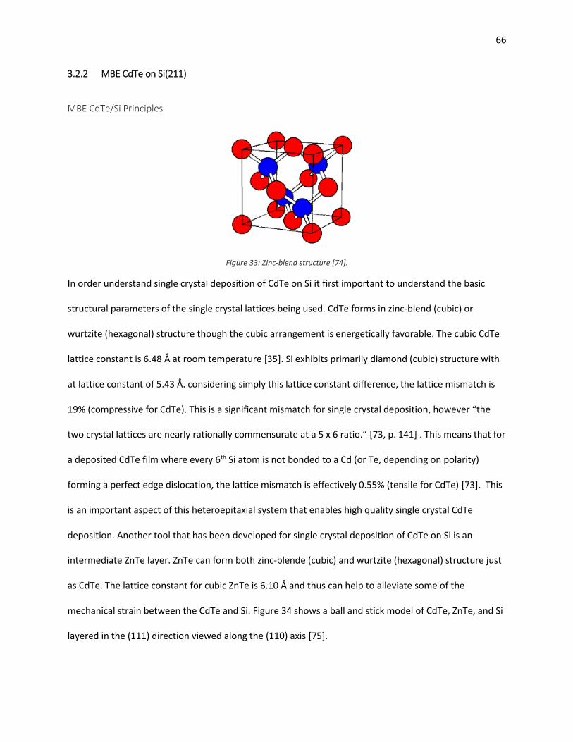
66
3.2.2 MBE CdTe on Si(211)
MBE CdTe/Si Principles
Figure 33: Zinc-blend structure [74].
In order understand single crystal deposition of CdTe on Si it first important to understand the basic
structural parameters of the single crystal lattices being used. CdTe forms in zinc-blend (cubic) or
wurtzite (hexagonal) structure though the cubic arrangement is energetically favorable. The cubic CdTe
lattice constant is 6.48 Å at room temperature [35]. Si exhibits primarily diamond (cubic) structure with
at lattice constant of 5.43 Å. considering simply this lattice constant difference, the lattice mismatch is
19% (compressive for CdTe). This is a significant mismatch for single crystal deposition, however “the
two crystal lattices are nearly rationally commensurate at a 5 x 6 ratio.” [73, p. 141] . This means that for
a deposited CdTe film where every 6th Si atom is not bonded to a Cd (or Te, depending on polarity)
forming a perfect edge dislocation, the lattice mismatch is effectively 0.55% (tensile for CdTe) [73]. This
is an important aspect of this heteroepitaxial system that enables high quality single crystal CdTe
deposition. Another tool that has been developed for single crystal deposition of CdTe on Si is an
intermediate ZnTe layer. ZnTe can form both zinc-blende (cubic) and wurtzite (hexagonal) structure just
as CdTe. The lattice constant for cubic ZnTe is 6.10 Å and thus can help to alleviate some of the
mechanical strain between the CdTe and Si. Figure 34 shows a ball and stick model of CdTe, ZnTe, and Si
layered in the (111) direction viewed along the (110) axis [75].

67
Figure 34: Si, ZnTe, CdTe (111) orientation lattice size [75]
Twin defects densities in HgCdTe have been shown to be reduced in films deposited on single crystal
CdTe(211) [76]. The B face has been shown to assist in the HgCdTe deposition process also [77]. As a
result, throughout years of development CdTe(211)B has been chosen as the preferred orientation for
subsequent HgCdTe deposition. Seeing as this was the primary application of CdTe on Si hetero-epitaxy,
the development of MBE techniques for CdTe(211)B on Si(211) has also been highly developed.
3 inch MBE CdTe(211)B/ZnTe(211)B/Si(211) Process
The MBE CdTe on Si process begins with substrate preparation. It is common to use an RCA type
cleaning process to prepare the 3 inch Si substrates prior to loading them into the introduction chamber
[78].The RCA process first an organic contamination clean in and ammonium hydroxide, hydrogen
peroxide, DI water solution. The Si wafer is then rinsed in DI water prior to an oxide strip in a dilute
hydrofluoric in DI solution. This step removes any oxide on the Si surface and can passivate the Si
dangling bonds with hydrogen. The typical RCA clean process continues with an ionic clean and thin re-
oxidation of the Si surface in a hydrochloric, hydrogen peroxide, in DI solution. This is again followed by
a rinse in DI water. The wafer is then dried using ultra-high purity nitrogen, placed on the molybdenum
sample holder and loaded into the chamber and pumped to UHV as fast as possible. This is to reduce the
chances of additional surface contamination. A fourth step can be added to terminated the surface with
hydrogen rather than an oxide by performing another hydrofluoric dip after the ionic clean and rinse.
While this is advantageous in that the hydrogen is more easily removed from the Si, process

68
repeatability has favored the oxide as a more reliable barrier of additional contamination while
transferring and loading into the MBE chamber.
Figure 35: Typical substrate temperature progress for single crystal CdTe on Si growth.
After transferring the sample into the growth chamber, a pre-deposition de-hydration bake is performed
at ~300°C. After this the sample is quickly heated to >850°C to desorb the oxide deposited during the
final step of the RCA process. At this point a Si RHEED pattern (see Section 3.2.3.4) should be observed
prior to cooling. As the substrate cools arsenic flux is supplied to help maintain the Si surface and
passivate the Si dangling bonds. The arsenic will preferentially bond to Zn and as such the arsenic
defines the B face polarity of the film. This arsenic passivation is followed by Te exposure to allow initial
Te bonding at the top of the Si(211) terrace. This is followed by migration enhance epitaxy (MEE) of
ZnTe using alternating material fluxes of Zn and Te while also giving time between each flux exposure to
allow surface migration of surface species. High quality layer-by-layer epitaxial growth is enabled using
this method, though it is slower than standard MBE. Following the approximately 15 nm deposition, The
ZnTe layer is annealed at ~380°C under Te flux. The Te flux is used to maintain the ZnTe surface during

69
the anneal as the high temperature would otherwise cause non-uniform desorption of the deposited
film potentially increasing surface roughness.
Following the anneal, the substrate temperature is reduced to ~220°C for CdTe deposition at a rate of
~1µm/hr. Throughout the CdTe growth, in-situ anneal are performed, heating to as high as 380°C under
Te and CdTe flux [75]. RHEED can be monitored at various points during the deposition to ensure high
quality crystal growth maintaining the (211) orientation. Figure 35 shows a typical substrate
temperature profile for single crystal CdTe(211) on Si(211) deposition.
CdTe Selective Area Epitaxy (SAE)
The techniques described in the previous section are useful for high-quality single crystal deposition of
large area CdTe on Si, however as part of this thesis selective area epitaxy (SAE) has also been
attempted in order to produce polycrystalline structural components in controlled ways. SAE relies on
differing sticking coefficients of two or more materials on the substrate surface. Here the material being
deposited should preferentially bond to one of the materials and as such deposit faster in location
where that material is present compared to regions of the other material(s). As these selective growth
regions continue to deposit vertically and laterally, they can overcome the growth domains present on
the other material(s) assuming the lateral growth has progress for long enough to encompass the other
material features. Previous work by Fahey at UIC has shown that the combination of CdTe and silicon
nitride (SiN) can allow for selective area growth and while there are other candidate material systems
this material combination demonstrated repeatability in successful SAE of CdTe by MBE [73]. Details of
the processing and patterning of these samples is discussed further in Section 5.2.2.

70
3.2.3 Characterization
3.2.3.1 Optical Imaging
Nomarski (Optical) Microscope
A Nomarski microscope is a standard optical microscope using a combination of magnifying lenses to
image either transparent (lighting from behind) or opaque (lighting from above) samples. What makes a
Nomarski microscope unique is the use of polarizing filters to enable differential contrast of the portions
of the sample through interference of the polarized light at the surface. This is often used to enhance
imaging of the boundaries and edges of surface features. In this thesis Nomarski microscopy is used
essentially as an optical microscope to observe general surface features however [79].
Optical Scattering
This imaging techniques is fundamentally very simple. We would like to be able to observe surface
roughness or small surface defects over a larger sample area. Generally a high quality crystalline film
look mirror smooth. [Reason] If we illuminate a sample at a low angle and image it from above, only
scattered light from surface defects will be imaged. In this way a smooth surface will look totally black
and any small defects will be seen and small bright dots. A rough surface will scatter a significant
amount of light back to the camera, and such will appears as a grey or white depending on the surface
roughness. Image processing for smooth surfaces may be able to be correlated with defect density.
A high resolution camera is held at a fixed distance from a sample surface. A separate flash bulb is held
near the surface of the sample, illuminating it from the side at a low angle. Finally some type of tube is
used to isolate any outside light from entering the imaging set up. Figure 36 shows a diagram of this
characterization set up and Figure 37 shows example data for 3” CdTe on Si of differing surface quality.

71
Figure 36: (a) Optical Scattering set-up (b) Schematic diagram of the basic principle of optical scattering. The Smooth surface scatters only a small portion of the incident illumination to the camera, while the rough surface scatters a significant portion of the incident light back to the camera.
Figure 37: 3” CdTe on Si Wafers images using the optical scattering setup. (left) The oxide was not fully removed during the deoxidation step of this sample and as a result there is a large central region of somewhat rough CdTe in addition to a large region of more highly rough CdTe in the first quadrant of the wafer. (center) This sample is more uniformly smooth as is indicated by the black color, however there is a large amount of macro-scale surface contaminants that can be observed by the large white specs in the image. (right) This wafer is smooth, but does still have some surface dislocations. These are seen by the very faint white specs in the image.
3.2.3.2 Fourier Transform Infrared Spectroscopy (FTIR)
FTIR is spectroscopic transmission or reflection measurement that operates in the infrared region of the
electromagnetic spectrum first developed for use in for astronomy in the 1950’s [80]. The principle of
operation is based on using the Fourier transform of a reflection or transmission signal as a function of

72
Michelson interferometer mirror position. Rather than attempt to scan through multiple wavelengths of
a broad spectrum light source using a diffraction grating, as is done with a spectrophotometer, the
broad spectrum source passes through an interferometer prior to reaching the sample surface. One of
the arms of this interferometer is then scanned in order to cause constructive and destructive
interference for different wavelengths of light in effect altering the wavelengths of light that can reach
the sample. This raw signal can then be converted from mirror position to wavelength through a Fourier
transform.
The electric field component of an electromagnetic plane wave can be defined by Equation 28.
�⃑⃑� = 𝐸0𝑒𝑖 (�⃑⃑� ∙�⃑� )�̂�
Equation 28
The time averaged energy density of an electromagnetic wave is defined by Equation 29,
⟨𝑈⟩ =𝑛2𝜖0
2|�⃑⃑� |
2
Equation 29
where the intensity is given by Equation 30.
𝐼 =𝑐
𝑛⟨𝑈⟩ = 𝐼0|�⃑⃑� |
2
Equation 30
Using this and the principle of superposition, we can solve for the expected intensity of two plane waves
interacting where one of those plane waves has traveled an additional distance 𝛿.
𝐼 = 𝐼0 |𝑒𝑖 (�⃑⃑� ∙�⃑� ) + 𝑒𝑖 (�⃑⃑� ∙(�⃑� +𝛿�̂�))|2
Equation 31

73
⇒ 𝐼 = 2 𝐼0(1 + 𝐶𝑜𝑠[𝑘 𝛿])
Equation 32
where 𝑘 = |�⃑⃑� | =2 𝜋
𝜆.
𝐼 is an even function. The total measured intensity 𝐼[𝛿] can thus be represented by integrating the signal
𝑆[𝑘] by the even Fourier component. Using Fourier reciprocity, the signal as a function of 𝑘 can be
determined.
𝐼[𝛿] = 𝐼𝛿=0 + ∫ 𝑆[𝑘]𝑒𝑖𝑘𝛿𝑑𝑘∞
−∞
Equation 33
⇒ 𝑆[𝑘] =1
2 𝜋∫ (𝐼[𝛿] − 𝐼𝛿=0)𝑒
−𝑖𝑘𝛿𝑑𝛿∞
−∞
Equation 34
This gives us a method for measuring the transmission or reflection of a sample by measuring the signal,
subtracting the background, and performing a Fourier transform.
This is useful for a variety of spectroscopic analysis, though in this thesis it is primarily used as means to
determine the thickness of a thin film. This is based on the principles of thin film interference as
described in Section 2.3.2.1
In this case the incident angle is 0, so the thickness is given by Equation 35.
𝑑 =𝜋
𝑛 ∆𝑘
Equation 35
*Note: 𝑘 =2𝜋
𝜆= 2𝜋𝜈

74
Certain criteria must be met in order for interference to occur however and a signal to be observed. First
the wavelength of the illumination must be significantly less than the thickness of the film for which you
are trying to determine the thickness. Second, the material must not be strongly absorbing in those
wavelengths. This limits the scope of applicability of this technique for determining sample thickness,
but is a very useful non-destructive method when the criteria are met.
Another aspect this type of spectroscopy in general is the influence of signal on the surface roughness of
the sample. As discussed in the optical scattering section, surface roughness can drastically change the
signal as a function of detector location. In the case of reflection or transmission interference, there is
the added complication of optical dispersion as a function of wavelength. Here shorter wavelength light
alters is trajectory in the material more strongly than longer wavelengths in general. This is not an issue
if the measurements are using normal incidence and detection with a smooth surface, but the normal
incidence condition is not maintained if the surface geometry is rough. The effect serves to attenuate
the signal for shorter wavelengths, and more strongly with rougher samples. Figure 38 shows typical
CdTe on Si signals for films of drastically different thicknesses.
Figure 38: FITR single point measurement for samples W13003 (Black, 1.6 µm) and W13008 (Blue, 17.5 µm)

75
3.2.3.3 X-Ray Diffraction (XRD)
XRD is a common crystallographic analysis techniques used in a variety of ways. It relies on principle of
elastic scatting of plane wave x-rays from nuclei in a crystal lattice interfering in to create a diffraction
pattern, the properties of which can be used to determine information about the sample. This principle
is typically introduced in the derivation of Bragg’s law (Equation 36) using techniques similar to those
necessary to derive the thin film interference equation (Equation 18).
2 𝑑 𝑆𝑖𝑛[𝜃] = 𝑚 𝜆
Equation 36
For crystallographic analysis it is useful to recast this using conventional Miller indices (Equation 37).
2 𝑑ℎ𝑘𝑙 𝑆𝑖𝑛[𝜃ℎ𝑘𝑙] = 𝜆
Equation 37
The planar spacing, d, for a cubic (zinc-blende) lattice with lattice constant, a, is given by Equation 38.
𝑑ℎ𝑘𝑙 =𝑎
√ℎ2 + 𝑘2 + 𝑙2
Equation 38
Using the reciprocal-space lattice vectors, G, it also common to express the constructive interference
condition as a possible change in momentum for elastically scattered x-rays.
∆𝑝 = ℏ ∆�⃑� = ℏ 𝐺
Equation 39
Both of these conventions arrive at the same result, though the latter is generally considered more
robust for complex crystallography.
The XRD systems used for this thesis use a fixed x-ray source with moveable sample stage and detector.
In this case θ is coupled to the detector position and sample stage position conventionally denoted ω.
2θ will always be associated with the detector position however. Seeing as XRD analysis in this thesis is
performed on primarily single crystal samples, it is important to understand the orientation of a

76
particular crystallographic plane with respect to the primary orientation of the wafer. The angle
between two planes, ϕ, is given by Equation 40.
𝐶𝑜𝑠[𝜑] = ℎ1ℎ2 + 𝑘1𝑘2 + 𝑙1𝑙2
√ℎ12 + 𝑘1
2 + 𝑙12√ℎ2
2 + 𝑘22 + 𝑙2
2
Equation 40
This condition in addition to lattice related diffraction conditions leads to only certain peaks being
observable for a given sample. It has become common to associate the (422) diffraction peak with the
crystal quality of (211) oriented lattice since a (211) peak is forbidden. The CdTe (422) peak for an x-ray
source with wavelength of 1.54 Å will occur at 2θ = 71.2°. It is common for the CdTe layer to be tilted on
the as high 5° off of the primary Si(211) plane in addition to the Si wafer manufacturing process not
being able to perfectly dice the wafer on the (211) plane leads to a typical ω position of the peak
occurring at (35.6) ± 3.5° depending on the rotational orientation of the wafer.
The shape of the double crystal rocking curve (DCRC, omega scan with fixed 2θ) depends on a number of
factors including fundamental quantum mechanical source wavelength broadening, imperfect source
wavelength isolation, sample curvature, small angle mosaic tilts and strain fields associated with
dislocations in the film. These contributions can lead to either Lorentzian or Gaussian broadening of the
rocking curve peak shape, however it is conventional to assume all contributions are Gaussian in order
to simplify analysis. As such Equation 41 can be used to represent the measured peak shape.
𝐼[𝜃] = 𝐼[𝜃0]𝑒−4 ln[2]
(𝜃−𝜃0)2
𝛽2
Equation 41
β in this form represents the full width at half max (FWHM) of the Gaussian peak shape. Seeing as the
final peak shape will be the multiplicative combination of the various Gaussian profiles associated with
the factors mention above, the full peak width, β, can be determined through some of the individual
broadening factors (Equation 42).

77
𝛽2 = 𝛽02 + 𝛽𝑖
2 + 𝛽ℎ2 + 𝛽𝑟
2 + 𝛽𝛼2 + 𝛽2
Equation 42
These contributions can be derived in various ways. In Table 7 below (Modified from “Table 4” in S.
Fahey’s Thesis [73, p. 68] ) these parameters are defined and values associated with the equipment used
in this thesis are given.
Table 7: FWHM (β) contributions [73]
FWHM Term Description Estimated Value
√𝛽02 + 𝛽𝑖
2 Intrinsic plus Instrumental Broadening 14”
𝛽ℎ Sample thickness (h in µm)
16.97
ℎ
𝛽𝑟 Sample curvature 7" 𝛽𝛼 Low angle tilts [81]
(D=Dislocation Density) √2 𝜋 (ln [2])𝑏2𝐷
𝛽 Dislocation strain [81] (b=Burgers Vector)
√0.09 𝑏2𝐷|ln[2 × 10⁻⁹√𝐷]𝑇𝑎𝑛2[𝜃ℎ𝑘𝑙]|
The FHWM to dislocation density correlation is an important result, as this provide a means for a non-
destructive characterization of the threading dislocation density.
Table 8: Generally accepted values of 422 peak FWHM for various material qualities.
Bulk CdTe
CdTe(211)/Si(211)
State-of-the-Art
Good Mediocre Poor Very Poor
~20” ~60” 70” - 80”
80” - 150”
150”-400”
>400”
Figure 39: Example CdTe XRD 422 DCRC
peak. FHWM=0.024°=86”
The system used in this thesis is a Bruker AXS Diffraktometer D8 system intended for high-resolution
single crystal X-ray diffraction measurements. This is an important distinction, because this system does
not produce enough signal for high quality polycrystalline XRD analysis, though it is capable of
measuring very narrow peak widths, < 20”.
Counts
ω (°)

78
3.2.3.4 Reflective High Energy Electron Diffraction (RHEED)
Reflective high energy electron diffraction (RHEED) is an in-situ characterization technique common to
many MBE systems. This characterization technique can provide information about crystal quality,
surface reconstruction, and deposition rate all in real time. This is done at glancing angle to the surface
so as not to substantially interfere with the deposition process. Due to the requirements of UHV
environment, and single crystal structural quality, this analysis technique is note found in many other
types of deposition systems.
A RHEED signal is most easily understood through the Ewald construction for diffraction. The fixed
incident electron wavelength and incidence direction specifies a wave number vector. The scattering
events can be considered elastic and as such the initially possible scatting directions form a sphere
(circle in 2 dimensions) with the center at the point of incidence. This is called the Ewald Sphere. Now if
we consider that constructive interference will only occur when the difference in moment is equal to a
reciprocal lattice vector, then the angles for which a diffraction peak will occur are those angles
associated with where the Ewald sphere meets a reciprocal lattice point.
In the case of RHEED, because of the glancing incidence and the very small wavelength of the high
energy electrons, a smooth surface will reduce the interaction in the real space z-dimension of the
lattice to only the top couple monolayers. In reciprocal space, this changes points to rods. Thermal
vibrations in the lattice give some width to the reciprocal space rods and the slight variation in electron
energy give some depth to the Ewald sphere. The diffraction pattern observed is then a real space
representation of the intersection of reciprocal lattice rods and the Ewald sphere. In this case the RHEED
pattern looks like smeared out points. If the sample remains single crystalline, but is roughened due to
non-uniform material desorption at high temperature for example, the electron beam will interact
through the features on the surface restoring the reciprocal lattice rods to points. The RHEED pattern in

79
this case will look like points, no longer smeared out. If the sample is polycrystalline, the diffraction
condition can be satisfied for and given rotation of the crystal and as such the RHEED pattern will appear
as half circle arches. Figure 40 shows typical RHEED patterns observed during single crystal CdTe
deposition process described in Section 3.2.2.
Figure 40: RHEED Patterns along the (110) axis for Si(211) {left} after the high temperature oxide desorb, and CdTe(211) {right} after ~10 µm growth.
3.2.3.5 Time Resolved Photo-Luminescence (TRPL)
Time resolved photoluminescence (TRPL) is an optoelectronic measurement used to determine the
effective minority carrier lifetime in a semiconductor material. The principle is to use a pulsed laser to
illuminate the material with light of energy greater than the sample material’s band gap to excite a large
number of carriers from the valence band to the conduction band. As these carriers radiatively
recombine, they will emit photons with energy approximately equal to or slightly less than the band gap.
By measuring the amount of light emitted by the sample at slightly below the band gap energy as a
function of time after the laser pulse, the carrier recombination lifetime can be extracted from the
exponential decay constants of the curve. This techniques has been used to characterize CdTe device
since the early 2000’s, where a strong correlation between lifetimes and open circuit voltage was
observed [82]. It is usually necessary to use a 2 exponential decay constants to accurately fit the data.
The second constant, τ2, is generally correlated with the effective minority carrier lifetime of the
material [83].

80
Figure 41: TRPL curves for a single crystal CdTe on Si sample at three different excitation powers (Black, Red, Green) compared with a bulk CdTe sample (purple), and the system response (Blue).
Recent developments of the TRPL systems has enabled two photon excitation processes to be used to
promote electrons to the conduction band in CdTe. This process works in the same way as standard
TRPL except that the excitation beam is sub band gap light that is highly focused with a primary focus
region of approximately 30 µm. In this high focus region, the intensity is great enough to promote
electrons to the conduction band via a double excitation process. Though a more difficult measurement
to perform, 2PE-TRPL has the advantage of allowing illumination of thick samples at various depths, or in
the case of thin samples, illuminating the entire sample thickness rather than just the first couple
microns. This has been used to extract a surface recombination velocity of 1.4x105 cm/s for a bulk single
crystal CdTe sample [84].
3.2.3.6 Hall
The Hall effect was discovered in 1879, where it was found that a voltage could be measured
perpendicular to current flow when a sample was also in the presence of a perpendicular magnetic field
[85]. This is a consequence of the two components of the Lorentz force, Equation 43.
𝑭 = 𝑞 (𝑬 + 𝒗 × 𝑩)
Equation 43

81
In 1948, Leo van der Pauw developed a now ubiquitous method for measuring various material
properties by taking advantage of the Hall effect. Using four contacts to form a square on a sample,
voltage is sourced to between two of the contacts at opposite corners to produce current, a fixed
magnetic field is applied perpendicular to the sample surface and the current flow and the Hall voltage is
measured across the other two corner contacts. By changing the direction of the applied voltage, the
direction of the magnetic field, and the contacts being used for the voltage supply vs. the Hall voltage
measurement, a variety of material parameters can be extracted. Two of the most important
semiconductor properties that can be extracted using this method, are the carrier concentration and the
mobility.
𝑉𝐻 =𝑉13 + 𝑉24 + 𝑉31 + 𝑉42
8
𝑛 =𝐼 𝐵
𝑞 𝑑 |𝑉𝐻|
𝑅𝑛𝑚,𝑘𝑙 =𝑉𝑘𝑙
𝐼𝑛𝑚
𝑅𝑣𝑒𝑟𝑡𝑖𝑐𝑎𝑙 =𝑅12,34 + 𝑅34,12 + 𝑅21,43 + 𝑅43,21
4
𝑅ℎ𝑜𝑟𝑖𝑧𝑜𝑛𝑡𝑎𝑙 =𝑅23,41 + 𝑅41,23 + 𝑅32,14 + 𝑅14,32
4
𝑒−
𝜋 𝑅𝑣𝑒𝑟𝑡𝑖𝑐𝑎𝑙𝑅𝑠 + 𝑒
− 𝜋 𝑅ℎ𝑜𝑟𝑖𝑧𝑜𝑛𝑡𝑎𝑙
𝑅𝑠 = 1
𝜇 =1
𝑞 𝑛 𝑑 𝑅𝑠
Figure 42: Van der Pauw method contact scheme used in this thesis, along with standard equations for calculation of carrier concentration, sheet resistance, and mobility.
For highly conducting samples, these measurements are often rather straightforward, as contacting
them can be done with relative ease. In the case of CdTe, the high work function makes this
measurement more difficult, in addition to the typically low carrier concentrations. It is important to
verify contact quality before completing the measurement. This is done by comparing the current

82
voltage (I-V) characteristics between all of the contacts. A poor contact will exhibit a roll over in the I-V
characteristic associated with a Schottky barrier. Good contacts will exhibit linear behavior throughout
the biasing range. We expect the material samples to be homogenous, so it is also important to verify
correct polarity associations of the Hall voltages in addition to the close to uniform resistance between
all contacts (spaced at equal distances). Examples of high and low quality measurements are shown in
Figure 43.
Figure 43 : Hall data for samples W13004, undoped (left) and W13032, doped (right). The data on the left is considered poor seeing as the I-V curves are highly non-linear and as such dynamic resistance is not constant. The symmetry of the voltage measurement is also not consistent and as a result the extracted data cannot be considered accurate. The data on the right, in contrast, is much higher quality, and as such the extracted data is expect to be accurate.
The Hall measurements for this these were performed using facilities at EPIR technologies. Graphite
(DAG paste) contacts were used in the configuration shown in Figure 42.

83
4 SINGLE CRYSTAL CDTE, STOICHIOMETRY, AND DOPING
4.1 MOTIVATION
The current, highly optimized, superstrate structure CdTe device is a complex system. As discussed in
Section 2.2.1, there are many interrelated layers and processing steps involved. Even the just the
polycrystalline nature of the CdTe material itself introduces a high level of complexity. This does not
prevent device and process optimization. New ideas can be tried and correlated with device
performance or other material quality metrics in order to make improvements and move the technology
forward. The subtlety is that the fundamental reasons for the improved performance become
convoluted in the complexly system. In order to do fundamental investigations, the complexity within
the material and device needs to be reduced. In this ways changes in material qualities or performance
can more easily be attributed to certain physical phenomena. This idea is the basis for the experiments
presented henceforth.
MBE single crystal CdTe on Si offers a number of benefits outline in the Chapter 1. Single crystal CdTe
deposited on Si by MBE has been used as an alternative substrate for HgCdTe infrared detector material
for the last two decades. In this role, the lattice orientation, surface quality, and dislocation density are
the most important material parameters. The electrical characteristics of the CdTe are not important in
this role. As such, while there has been substantial development of the single crystal CdTe deposited by
MBE on Si the focus has only ever really been on the structural properties. The knowledge base
developed for this application does provide a useful starting point for fundamental CdTe material
research for solar photovoltaic applications however.
83

84
Figure 44: Single Crystal CdTe project diagram
4.2 EXPERIMENTS
4.2.1 Thickness Variation Baseline
In order to establish various baseline measurements for single crystal CdTe deposited on Si, a set of
samples were deposited with varying CdTe thicknesses. CdTe(211)B orientation is preferred for HgCdTe
growth, and the recipes developed for the last decade have been optimized around this requirement. As
such, in order to produce the high material quality with the least amount of recipe optimization growths
needed, the techniques developed for CdTe(211)B growth are used. The material layer structures are
shown in Figure 45.
Figure 45: Thickness variation baseline sample stacks.

85
The specific growth recipe for each sample was very similar to that described in Chapter 3 with the
differences being in the number of in-situ anneal cycles, total growth time and CdTe deposition rate.
These depositions all went well, with appropriate RHEED transitions seen. The 1.5 μm sample had no in-
situ anneals while the 7.5 μm sample had 3 anneals. The 10 μm and 18 μm samples had five anneals.
These anneals are always equally spaced throughout the deposition. Deposition rates between the 1.5
μm, 7.5 μm, and 10 μm samples were very similar, however the rate was increased for the 18 μm
sample leading to the thicker film.
Following deposition, each layer is initially characterized by single point XRD (<422> DCRC) and FTIR
(thickness). Full 3” wafer mapping for both XRD and FTIR is then completed using the facilities at EPIR
Technologies Inc. The surface quality is examined and in most cases an optical scattering image is taken
for direct comparison. Pieces of each 3” wafer are also sent to NREL for lifetime characterization using
TRPL. The 2 photon excitation (2PE) TRPL technique has proven to be the most reliable and as such
results for the τ2 values of the 2PE-TRPL measurement are used to compare all films. The results for this
experiment are summarized in Table 9. Figure 46 shows the 3” wafer mapping results for these samples.
Table 9: Summary table for thickness variation baseline samples.
MBE Layer ID
FTIR Thickness
{ Average ± Stdv } (μm)
XRD (422) DCRC FWHM
{Average ± Stdv} (Arcsec)
XRD (422) DCRC FWHM
{Min,Max} (Arcsec)
2PE-TRPL Lifetime
{τ2} (ns)
W13003 1.63 ± 0.03 416 ± 15 392, 459 0.05
W13004 7.20 ± 0.17 119 ± 27 101, 232 0.8
W13007 9.2 ± 0.32 190 ± 81 101, - 1.04
W13008 17.55 ± 0.32 93 ± 40 67, 246 2.3

86
Thickness(μm)
W13003
Center = 1.65 μm
W13004
Center = 7.44 μm
W13007
Center = 9.6 μm
W13008
Center = 18.13 μm
FWHM(Arcsec)
Average = 416”
Average = 119”
Average = 190”
Average = 93”
Figure 46 : FTIR Thickness and XRD <422> DCRC FWHM wafer maps
Generally it is expected that crystal quality will trend with CdTe thickness. It is currently understood that
dislocations associated with FWHM broadening have a better chance of annihilating if the layer has
been grown thicker and because the X-rays primarily sample the top several microns of the film, the
FWHM improves. The in-situ anneals assist in the migration and annihilation of these dislocations also.
The reduced uniformity of the 10 μm sample (W13007) is not fully understood. The cleaning procedure
was being optimized when this sample was deposited and poor cleaning may have resulted in poorer
layer uniformity and quality than expected. The same dislocations associated with broadening of a DCRC
FWHM are suspected to lead to enhanced recombination. As, such it would be expected that as the
crystal quality improves (as measured by XRD) the recombination rate should also improve. Figure 47 is
a plot of FWHM vs. recombination lifetime (τ2) as measured by 2PE-TRPL.This trend is most apparent
when comparing the minimum FWHM to τ2. This is to be expected since the TRPL measurements are
generally performed in regions of highest crystal quality.

87
Figure 47: Plot comparing crystal quality (FWHM) to recombination rate (τ2).
𝜏2 =9096
𝛽𝑚𝑖𝑛2
Equation 44
Fitting the minimum FWHM to 2PE-TRPL lifetime results in the empirical relation found in Equation 44.
The recombination lifetimes measured are substantially lower than would be expected of high quality
single crystal material however. This shorter lifetime is believed to be associated with surface
recombination. If the bulk crystal lifetimes for this material are substantially longer than the lifetimes
associated with surface recombination, the total effective lifetime is approximately equal to the surface
recombination lifetime.
1
𝜏=
1
𝜏𝑏𝑢𝑙𝑘+
1
𝜏𝑠𝑢𝑟𝑓𝑎𝑐𝑒
Equation 45
𝜏𝑠𝑢𝑟𝑓𝑎𝑐𝑒 =ℎ
2 𝑆
Equation 46
Where h is the thickness of the film and S is the surface recombination velocity. The effective lifetime
should be directly proportional to sample thickness in this case. This is particularly true for the 2PE-TRPL
0
0.5
1
1.5
2
2.5
3
50 150 250 350 450
Life
tim
e (n
s)
XRD DCRC FWHM (arcsec)
XRD MinXRD Avg w/ Stdv

88
measurement seeing as the large focal distribution of the illuminating beam allows for carriers to be
generated throughout the epitaxial layer. Figure 48 shows a plot of thickness vs. lifetime along with a fit
using Equation 46.
Figure 48: Carrier recombination Lifetime plotted vs. CdTe layer thickness.
The surface recombination velocity is determined to be 4.15 x 105 cm/s from the fit. This is a high
surface recombination velocity and trend of crystal quality with sample thickness is confused slightly by
this result. Crystal quality does improve with epitaxial layer thickness and as such the empirical relation
found in Equation 44 is expected to be more coincidental than directly motivated by physical
phenomena.
Surface Passivation
In an attempt to mitigate the effects of the surface, a short passivation experiment was performed. The
general principle is to minimize the number of carriers that can reach the surface and passivate the
dangling bonds at the interface. In general there is a tradeoff between surface recombination and
interface recombination. Type-II band alignment helps to mitigate this by creating a barrier for carrier
types. As can be seen in Figure 49, several materials have the appropriate Type-II band alignment
desired for surface passivation of CdTe, namely ZnS, ZnSe, and ZnTe.

89
Figure 49: Natural band offsets for various II-VI materials. Su-Huai Wei and Alex Zunger, Calculated natural band offsets of all II–VI and III–V semiconductors: Chemical trends and the role of cation d orbitals, Appl. Phys. Lett.. 72, 2011 (1998) [86]
We have deposited ZnS by e-beam on pieces of thickness variation CdTe samples. Prior to deposition,
the sample surface is cleaned using a short Br:MeOH etch. This is meant to remove a thin layer of the
CdTe and with it any potential contamination such as thin oxide layers.
After deposition, the pieces were sent to NREL for lifetime measurement using 2PE-TRPL. The passivated
films exhibited lifetimes essentially identical to their unpassivated counter parts. There are a variety of
reasons that could explain this result, however the two most relevant are (1) the recombination lifetime
τ2 is not dominated by surface effects and as such the passivation had not effect or (2) the surface
passivation was ineffective as implemented. The second is more likely the case seeing as the thickness
and minority carrier lifetimes measured by 2PE-TRPL are nearly directly proportional. Assuming the
passivation layer was stable for the few weeks between deposition and measurement, interface
recombination may be taking the place of surface recombination.
4.2.2 Tellurium Overpressure
Elemental tellurium overpressure is used in the standard MBE deposition of CdTe(211)B on Si(211) at
several points in typical growth recipes. The first comes in locking in the (211)B orientation following the
arsenic monolayer silicon passivation. This is followed by MEE deposition of ZnTe where elemental
source of Zn and Te flux are alternated to deposit a very high quality ZnTe(211)B layer. Finally, it has
been found that Te overpressure during in-situ anneals assists in stabilizing the surface and preventing
Ener
gy (
eV)

90
loss of surface integrity through minimization of CdTe re-sublimation [87]. As such most (if not all) CdTe
MBE deposition systems are equipped with an elemental Te source.
The role of Te is investigated here for a different purpose however. Stoichiometric adjustment of a
depositing film is expected to change the chemical potential of the system and as a result alter the
formation energy of various defects.
Figure 50: Formation energies as a function of Fermi Level in the Te-rich limit [88].
Intrinsic CdTe is generally slightly p-type due to Cd vacancies. Te overpressure could enhance this
behavior by further reducing the formation energy of Cd vacancies. In the case of cation (Cd) site
doping, this is could be advantageous by increasing the availability of cation sites [88]. A more complete
understanding of the behavior of films deposited in Te overpressure is desired and as such a set of films
of various thicknesses and Te overpressures have been deposited to study this behavior.
Four layers with Te overpressure were deposited, all with target thicknesses of 10 μm. Standard RCA
cleaning, in-situ deoxidation, arsenic passivation, and ZnTe MEE processes were performed prior to
deposition. 5 in-situ anneals were performed during each deposition also. As with the previous study,
following deposition is characterization by XRD, FTIR and optical imaging. Fully characterized wafers are

91
divided into piece some of which were sent to NREL for 2PE-TRPL recombination lifetime
measurements. The amount of Te overpressure was initially measured directly using a ratio of the Te
source QCM reading to the CdTe source QCM reading. This was referred to as QCM%. While this value is
useful for run to run comparison of additional Te, it does not correctly represent the Te to Cd ratio
reaching the sample. It is also difficult to correlate this with the more common MBE flux measurement
of beam equivalent pressure (BEP). As such a conversion from the QCM reading to atom per second has
been established and is discussed in Chapter 3. One must be careful to correctly consider the molecular
species associated with the beam flux. Here I represent the overpressure values by a direct ratio of the
number of atoms of a particular element incident on the surface per second. CdTe sublimates
congruently according to the flowing reaction.
𝐶𝑑𝑇𝑒𝑠 → 𝐶𝑑𝑔 + 1
2𝑇𝑒2
𝑔
As such despite the fact that the total Te pressure is half that of the Cd because of the formation of Te
dimers, the total number of individual atoms is still the same. So for typical depositions the Cd:Te ratio is
1:1. Table 10 summarizes the layers deposited as part of the Te overpressure study.
Table 10: Te Overpressure summary table.
MBE Layer ID
Cd : Te
FTIR Thickness
{ Average ± Stdv } (μm)
XRD (422) DCRC FWHM
{Average ± Stdv} (Arcsec)
XRD (422) DCRC FWHM
{Min,Max} (Arcsec)
2PE-TRPL Lifetime
{τ2} (ns)
W13010 1 : 1.5 6.31 ± 0.38 104 ± 11 95, 146 1.07
W13029 1 : 1.5 14.36 ± 0.3 71 ± 3 65, 81 1.7
W13009 1 : 1.9 10.66 ± 0.27 74 ± 3 71, 216 1.8
W13028 1 : 2.4 14.81 ± 0.24 73 ± 2 69, 78 1.7

92
Thickness(μm)
W13010 Te : 1.5
Center = 6.54 μm
W13029 Te : 1.5
Center = 14.86 μm
W13009 Te : 1.9
Center = 11.15 μm
W13028 Te : 2.4
Center = 15.19 μm
FWHM(Arcsec)
Average = 104”
Average = 71”
Average = 74”
Average = 73”
Figure 51: Thickness and FWHM Maps for Te overpressure samples.
These depositions had a significant amount of variability in the MBE process. This was due to waning
CdTe source material coupled with an increased deposition rate associated with the addition of Te
overpressure. The effect of increased deposition rate with Te overpressure was not initially observed
due to the deposition taking place with a limited amount of CdTe source material. Sample W13009 was
very close to the target thickness, but the source material ran out during the deposition of W13010
resulting in a much thinner film. Using a standard calibrated CdTe flux with ample source material for
depositions W13028 and W13029, resulted in a nearly 50% increase in deposition rate with the addition
of Te overpressure. The Te ratio for W13029 was the same as W13010 in order to be more comparable
with the other samples in the set as well as previous depositions without Te overpressure.
We currently have two ideas that could explain the increased deposition rate with additional Te
overpressure. The first relies on the fact that Te vapor is a dimer that must dissociate in order to deposit
epitaxially. Because of this additional energy barrier, despite having equal numbers of Cd and Te
available at the surface of the depositing film, the number of elemental Te species available for epitaxial
bonding is less than the elemental Cd. After initial physisorption, Cd and Te dimers migrate on the

93
surface before being chemisorbed at an epitaxial bonding site. For every 2 Cd atoms there is 1 Te dimer.
If there is not enough energy available for the Te to dissociate, it will re-evaporate. If equal number of
Cd atoms and Te dimers re-evaporate, there will be a net deficiency of Te on the surface. Additional Te
overpressure may help to reduce this deficiency. The second explanation is related to epitaxial CdTe
behavior during in-situ anneals. The current understanding for why Te overpressure should be used
during these anneals is to prevent loss of CdTe material and as a result loss of surface quality due to re-
evaporation. The idea is that if Te vapor is present at the surface, it will be more difficult for CdTe to
sublimate, for the same reason that it takes higher temperatures to boil water at higher pressures. In
the case of Te overpressure during CdTe deposition, there is already pressure being supplied by the
CdTe. That said, more pressure from the Te source will still add to the effect of preventing re-
evaporation of surface species. The net effect in this case is faster deposition due to less re-
evaporation, and improved surface quality. That said both of these effects, or something else entirely
may explain the observations.
The most notable material change in material properties with the addition of Te overpressure, is the
significantly improved crystal quality. There is both and overall decrease in average FWHM as well as a
substantial decrease FWHM standard deviation. This improved crystal quality is mirrored in the 2PE-
TRPL recombination lifetimes. Figure 52 shows 2PE-TRPL lifetime and Average FWHM with standard
deviation plotted against the Te ratio for each deposition.
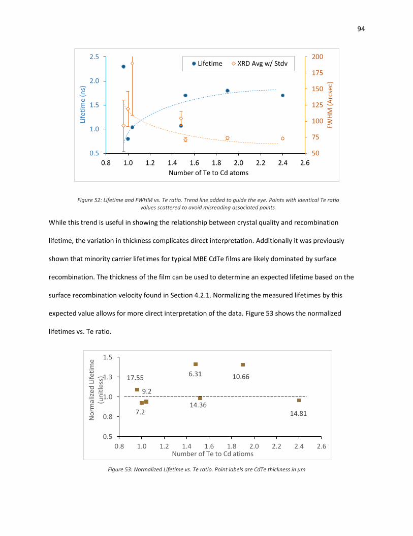
94
Figure 52: Lifetime and FWHM vs. Te ratio. Trend line added to guide the eye. Points with identical Te ratio values scattered to avoid misreading associated points.
While this trend is useful in showing the relationship between crystal quality and recombination
lifetime, the variation in thickness complicates direct interpretation. Additionally it was previously
shown that minority carrier lifetimes for typical MBE CdTe films are likely dominated by surface
recombination. The thickness of the film can be used to determine an expected lifetime based on the
surface recombination velocity found in Section 4.2.1. Normalizing the measured lifetimes by this
expected value allows for more direct interpretation of the data. Figure 53 shows the normalized
lifetimes vs. Te ratio.
Figure 53: Normalized Lifetime vs. Te ratio. Point labels are CdTe thickness in μm
50
75
100
125
150
175
200
0.5
1.0
1.5
2.0
2.5
0.8 1.0 1.2 1.4 1.6 1.8 2.0 2.2 2.4 2.6
FWH
M (
Arc
sec)
Life
tim
e (n
s)
Number of Te to Cd atoms
Lifetime XRD Avg w/ Stdv
17.55
7.2
9.2
10.666.31
14.8114.36
0.5
0.8
1.0
1.3
1.5
0.8 1.0 1.2 1.4 1.6 1.8 2.0 2.2 2.4 2.6
No
rmal
ized
Lif
etim
e (u
nit
less
)
Number of Te to Cd atioms

95
Points greater than 1 (dashed line) line exhibit lifetimes longer than predicted by the thickness and
surface recombination velocity while points less than 1 exhibit shorter lifetimes than would be
predicted. Normalized lifetime values for the 1.0 Te ratio samples exhibit are within 10% of the expected
value of 1. The 14 µm samples show normalized lifetime values within this 10% range. The two thinnest
samples have measured lifetimes substantially higher than would be expected from films without Te
overpressure but the same thickness however. The relationship does not appear to be linear as both of
the thinner film exhibit 40% enhanced recombination lifetime despite a more than 4 μm thickness
difference.
This is a potentially interesting result, though it is difficult to explain with the current data set. It is
possible that Te overpressure of any significant amount is assisting the mitigation of defects that lead to
enhanced recombination in the bulk and at the surface, but this conclusion cannot be directly
substantiated from this data.
The use of Te overpressure for improved crystal quality uniformity may be useful in the realm of
epitaxial CdTe deposition and potentially single crystal II-VI solar cell fabrication, but the benefits
associated with Te overpressure for improving crystal quality may be less substantial in the high
pressure, fast deposition techniques required for high throughput mass production of thin film modules.
That said, investigation of how Te overpressure effects polycrystalline material given typical MBE growth
parameters may still be worth investigating.
4.2.3 P-type CdTe Doping
As with most semiconductor devices, doping control is very important as a means to control device
performance. Carrier type, concentration, and doping profile control can enable complex device
architectures that may enable enhance performance. In the case of thin-film CdTe photovoltaics, the

96
primary concern with regard to doping is the acceptor carrier concentration in the CdTe absorber
material.
Doping in-situ with MBE may offer enhanced doping profile control, as compared to other techniques
such as diffusion or implantation doping. That said, the work presented here is meant to address the
carrier concentration first and foremost. We would like to develop an understanding of epitaxial CdTe
deposition techniques that can enable p-type carrier concentrations as high as 1017 cm-3. Achieving CdTe
carrier concentrations at that level would start to match the carrier concentration typically found in the
CdS n-type layer.
There are a number of dopants to be considered with regard to p-type doping. Often there is a trade-off
between a material that is easily incorporated and one that is stable. Presented here is work that has
been done to investigate nitrogen and arsenic as p-type dopants. Both are anion, Te, site dopants. This
poses a bit of challenge for CdTe doping since the CdTe is typically slightly cation, Cd, deficient. It is
suspected that cation overpressure will assist incorporation of these dopants. Some difference in source
material are worth noting in comparing nitrogen and arsenic as p-type dopants. Nitrogen is a gas at
room temperature meaning that a typical effusion cell cannot be used. In the work presented here, a
plasma source is used to supply nitrogen ions to the depositing film surface. Arsenic is a solid and can be
deposited with a standard effusion cell. The primary vapor component in this case is As4 however and
previous doping work with HgCdTe had found that this vapor species is not easily incorporated into
CdTe. As such an arsenic cracker source is used to supply As2 to the depositing film surface. With regard
to the use of cation overpressure, Cd3As2 is also investigated as a means to supply both arsenic and
cadmium. The results of these investigations are presented in the following sections.

97
4.2.3.1 Nitrogen Doping
In collaboration with EPIR technology, nitrogen plasma doping form improved carrier concentration in
CdTe, CdZnTe, and ZnTe has been investigated [89]. Nitrogen doping of II-VI materials using a nitrogen
plasma source was investigated significantly by Baron et. al. [90, 91, 92], though they used single CdTe
substrates rather than Si. The primary goal of this research was for application in multi-junction single
crystal II-VI on Si based solar cells [93]. Standard MBE deposition techniques were used while adjusting
ZnTe to CdTe ratios for the desired Zn%. Plasma sources typically require process gasses to be supplied
at pressures high than is desired for typical MBE operation. In order to maintain a reasonably low
background pressure for the depositions, a low conduction nozzle plasma source in combination with a
low flow mass flow controller enable both good source ionization and pressure control while
maintaining plasma. The amount of nitrogen in the samples is adjusted by varying ratios of argon and
nitrogen in the process gas supply.
The most significant trend observed in this data set was the significant dependence on achievable
carrier concentration with increasing Zn%. This trend mimicked the results of Baron as can be seen in
Figure 54. Unfortunately, due to this trend, carrier concentrations were never reliably measured for any
of pure CdTe samples attempted.
Figure 54: Hole concentration (left) and mobility (right) plotted compared to Zn concentration. Results of uniform and pulse doping techniques from Baron, et al. are plotted for reference [89].

98
The general explanation for the trend is generally associated with Zn-N bond bond length being more
similar to Zn-Te bond length than the Cd-N compared to the Cd-Te bonds. The increased strain need to
maintain the nitrogen on the Te sites in CdTe prevents significant incorporation. It should be noted that
CdZnTe is a more strain system than CdTe in general however. The arsenic doping work discussed in the
following section reveals a potential trend of higher dopant incorporation in more defective material,
and the nitrogen incorporation results similar.
4.2.3.2 Arsenic doping
As previously mentioned arsenic has been used as a p-type dopant in MBE deposited HgCdTe for years
[69]. This technology was developed in order to facilitate high quality infrared detection diodes. During
the early stages of that research it was determined that it was difficult to incorporate the As4 molecules
supplied by typical As effusion cells. As such, arsenic crackers, common to the III-V MBE community,
started being used to supply As2 which was much more easily incorporated. P-type doping of HgCdTe
with as requires the arsenic to sit on the Te site just as is the case with pure CdTe. The high vapor
pressure of Hg means that the deposited film typically incorporates the As on interstitial or Cd/Hg sites
however. In order to activate the As, move it from the interstitial and Cd/Hg sites to the Te sites, an ex-
situ activation anneal is performed. This is done in a Hg overpressure, to help prevent further loss of Hg
from the film. Following the activation anneal is a long Hg vacancy filling anneal. Here the sample is kept
at elevated temperatures with a Hg overpressure. The excess Hg can diffuse into the material
maintaining the Cd-Hg x value (desired band gap) while keeping the As on the As on the Te sites. This
research was quite successful and enabled nearly 100% activation and carrier concentrations greater
than 1018 cm-3 in HgCdTe [69].
Using this previously developed knowledge base, the initial investigations presented here are aimed at
reproducing the success achieved in the HgCdTe community with CdTe. Recent work at EPIR
technologies has resulted in p-type carrier concentration of 1016 cm-3. They found that low

99
concentration of incorporated arsenic quickly rise as the depositing film thickness increases. The crystal
quality as measured by XRD FWHM was also degraded as compared to undoped films of similar
thicknesses [94].
Preliminary Samples
The first arsenic doped CdTe samples produced at UIC used a thick undoped CdTe buffer layer as a
means to improve the crystal quality prior to doping. This undoped layer can also as an electrical
insulator for Hall measurements, ensuring that the electrical characteristics extracted are a result of the
doped film and not the substrate. As with previous experiments, standard processing and deposition is
performed through the first 10 to 12 microns of CdTe with 5 in-situ anneals. Unfortunately, due some
likely inaccurate thermocouple measurements, the oxide desorption step for these sample was much
longer (>30 minutes) than is typically desired (~5 minutes). Keeping the Si at high temperatures for an
extended period of time tends to cause surface quality degradation. As such, the CdTe crystal quality
may suffer also. Following the CdTe deposition 5 microns of CdTe is deposited with As2 overpressure
supplied by the arsenic cracker. No anneals are performed during this portion of the growth to limit the
potential for loss of As or limit incorporation due to additional Te. Following deposition the 3” wafers
are characterized using FTIR and XRD then divided into pieces, some of which are sent to NREL for 2PE-
TRPL measurement. Table 11 and Figure 55 summarize the sample properties.

100
Table 11: Arsenic cracker doped CdTe with thick buffer layer Table
Cd : Te : As 6.8 : 6.8 : 1
or 1 : 1 : 0.15
MBE Layer ID
FTIR Thickness { Center }
(μm)
XRD (422) DCRC FWHM
{Average ± Stdv} (Arcsec)
2PE-TRPL Lifetime
{τ2} (ns)
W13026 16.7 369 ± 131 ?
W13027 19.3 337 ± 110 ?
Figure 55: Thick Buffer CdTe:As2 sample stacks
Thickness(μm)
W13026
Center = 16.69 μm
W13027
Center = 19.33 μm
FWHM(Arcsec)
Average = 368.9”
Average = 337.9”
Figure 56: FWHM and Thickness Maps for preliminary arsenic doped CdTe samples
Crystal quality for these samples is notably poor and non-uniform. This is likely due to both the arsenic
incorporation coupled with the long outgassing process. There seems to be some inconsistencies FTIR
thickness measurement also, though most of center portion of the sample is as uniform as any of the
other standard samples. The crystal quality degradation is consistent with the observations from EPIR,
which means that even with a thick undoped buffer layer, the addition of As without further recipe
modification results is poor quality CdTe. SIMS was performed on small pieces of these sample in order
to develop a better understanding of the arsenic incorporation throughout the films. Figure 57 shows
the SIMS profiles measured by Evans Analytical Group for each of the preliminary samples.

101
Figure 57: SIMS profiles for preliminary arsenic incorporated samples.
The difference in thickness of the buffer layer is apparent in the profiles as the difference in size of the
low-arsenic-incorporation region after the first 5 to 6 microns. At the surface of the sample the As cap
that was deposited in the case of sample W13026 is apparent as the arsenic concentration spikes near
the surface. The incorporation rate is essentially the same between the two samples and notably high,
near 1021 cm-3. Given the high incorporation rate observed for these samples it is conceivable that a
more modest incorporation, 1017 to 1018 cm-3, may lead to improved crystal quality.
In an attempt to reproduce the results achieved by EPIR and the HgCdTe community, ex-situ activation
and diffusion anneals are also performed. Hg overpressure is also used seeing as the methods for that
process have already been developed and optimized. Following these anneals, graphite contacts are
made on the CdTe surface in the Van-der-Pauw configuration using colloidal graphite paste. In order to
ensure good contact is made, a 10 minute contact anneal is performed with a nitrogen overpressure.
Finally Hall measurement is performed using the Ecopia HMS-3000 system at EPIR Technologies, Inc.
Activation anneals of 440°C and 480°C were both attempted in addition to contact anneal of 350°C and
1E+00
1E+01
1E+02
1E+03
1E+04
1E+05
1E+06
1E+07
1E+16
1E+17
1E+18
1E+19
1E+20
1E+21
1E+22
0 2 4 6 8 10 12 14 16 18 20
Se
co
nd
ary
io
n in
ten
sity (
co
un
ts/s
ec)
Co
nce
ntr
atio
n (
Ato
ms/c
m3)
Depth (µm)
As_27 As_26
Te_27 Te_26

102
400°C. Unfortunately only a very limited number of these samples had low enough contact resistance to
trust the Hall measurement. Table 12 summarizes the best results for each MBE layer.
Table 12: Preliminary arsenic doping results.
*Contact check failed
This is a promising result in that we were able to achieve carrier concentrations using these methods
greater than those typically achieved in superstrate configuration px-CdTe devices, but there is certainly
room for improvement. The following is a list of aspects of this process and material that we would like
to improve.
1) Carrier Concentration: while mid 1015 cm-3 is good, control of doping level to on the order of 1017
would be preferred. This carrier concentration is desired to enable a substantially higher Voc, on
the order of 1 Volt.
2) Activation Percentage: Currently we assume that these samples had nearly the amount of
arsenic incorporated as the piece that had SIMS analysis done, the activation percentage is
significantly less 1%. The HgCdTe community was able to achieve nearly 100% activation and
EPIR-NREL were able to achieve activation percentages near 50%.
3) Repeatability/Uniformity: The crystal quality of these samples was quite poor. In addition we
were only able to measure a carrier concentration with Hall for a couple samples with specific
processing performed. Ideally, we would be able to achieve decent doping and activation
process repeatability for a large number of samples from the same 3” wafer.
MBE Layer ID
FTIR Thickness
(μm)
XRD (422) DCRC FWHM
(Arcsec)
Activation Anneal Temperature
(°C)
Contact Anneal Temperature
(°C)
Hall Carrier Concentration
(cm-3)
Hall Mobility (cm2/V∙s)
W13026 16.7 170 480 350 6.1E+15 43.5
W13027 19 188 480 400 1.6E+13* 15.2*

103
As cracker (As2) vs. Cd3As2 effusion (Cd + As4)
Given the results of this preliminary work and some of the desired improvements, another small sample
set was produced, this time comparing the use of the arsenic cracker source compared to the use of a
Cd3As2 effusion source. There are benefits and drawbacks to each of these choices. The first aspect of
this choice to note is the composition of the molecular beam created by each of these source. For an As
cracker source operating in the cracking most of the arsenic vapor is in the form As2 molecules [67]. For
simplicity I will assume that arsenic vapor is produces according to the reaction in Equation 47.
𝐴𝑠𝑠 → 1
2𝐴𝑠2
𝑔
Equation 47
Cd3As4 on the other hand produces primarily As4 vapor [95] and for simplicity I will assume this takes
place according to the reaction found in Equation 48.
𝐶𝑑3𝐴𝑠2𝑠 → 3 𝐶𝑑𝑔 +
1
2𝐴𝑠4
𝑔
Equation 48
Now, As2 is known to be more easily incorporated into epitaxial HgCdTe [69] and it is assumed that
similar behavior will be found in the case of CdTe. This gives an advantage to the arsenic cracker. That
said we are trying to dope CdTe using the arsenic, and excess Cd is expected to facilitate As finding Te
vacancies which is the appropriate site for the p-type doping. I this way, the Cd3As2 source allows for
supply of both cadmium and arsenic and as such may be very useful in p-type doping of CdTe.
These samples were produced using standard processing techniques and conditions with the exception
of the additional dopant source flux supplied after the first 1 µm of CdTe deposition. As mentioned
previously, the MBE system used for this work relies on a QCM deposition rate measurement for flux
calibration. As such, the parameter used to compare flux ratios when these samples were initially
produces was simply the QCM rate ratio. Unfortunately due to the substantial difference in flux

104
constituents between the arsenic cracker source compared to the Cd3As2 effusion source, the 2% flux
ratio used as a constant for these two samples actually results is very different elemental species ratios
incident on the surface. These ratios are found in Figure 59. Following deposition, standard XRD and
FTIR characterization is carried out. The samples are divided and pieces are sent to NREL for 2PE-TRPL
measurement.
Table 13: Cd3As2 vs. As cracker doped CdTe summary table
Cd : Te : As Shown in Figure 59
MBE Layer ID
FTIR Thickness
{Average ± Stdv} (μm)
XRD (422) DCRC FWHM
{Average ± Stdv} (Arcsec)
2PE-TRPL Lifetime
{τ2} (ns)
W13032 9.06 ± 0.19 256 ± 184 ?
W13041 11.9 288 ± 437 ?
Figure 58: CdTe:Cd3As2 vs. CdTe:As2 sample stacks
Thickness(μm)
W13032 – Cd3As2 51.6 : 47.6 : 1
Center =9.40 μm
W13041 – As cracker 6.8 : 6.8 : 1
(Mapping Data Not Taken)
Center = 11.91 μm
FWHM(Arcsec)
Average = 256”
Average = 288”
Figure 59: FWHM and Thickness Maps for preliminary arsenic doped CdTe samples
Following the deposition of W13032, several portion of the sample from regions with differing crystal
quality were further processed for Hall measurement. The same annealing and contacting schemes
described in the previous section were used. Samples with the 440°C activation anneal did not result in

105
any measureable carrier concentration. The 480°C activation anneal along with the two different contact
anneal temperatures did result in measurable carrier concentrations however. The carrier
concentrations and mobilities measured are plotted in Figure 60.
Figure 60: Hall results for pieces of W13032 with differing crystal quality
The data seems to indicate that higher carrier concentrations can be achieved in regions with poorer
crystal quality. Higher mobilities are found in regions of poorer crystal quality also. The increased
contact anneal temperature also shows improvement of all parameters. The mobility increase despite
poorer crystal quality is an unexpected result. In order to further understand the carrier concentration
increase and also further investigate the amount of arsenic activation in the sample, SIMS analysis is
performed on samples from regions of good crystal quality (FWHM~100”) and poor crystal quality
(FWHM~250”). The data is plotted in Figure 61.
5
10
15
20
25
30
5E+14
1.5E+15
2.5E+15
3.5E+15
4.5E+15
5.5E+15
50 100 150 200 250 300
Mo
bili
ty
(cm
2/V
∙s)
Car
rier
Co
nce
trat
ion
(1
/cm
3 )
XRD <422> DCRC FWHM (Arcsec)
CC 350 CC 400 Mobility 350 Mobility 400

106
Figure 61: SIMS for two regions of sample W13032, one with good crystal quality and the other with poor crystal quality.
As might have been expected the sample with the higher crystal quality had lower incorporation at level
of 5 x 1015cm-3 uniformly throughout the doped layer. The sample from the region with poor crystal
quality shows a “saw-tooth” incorporation pattern with an average level of approximately 1 x 1016 cm-3.
The saw-tooth pattern correlates well with the in-situ anneals performed throughout the deposition.
This may be more evidence for crystal quality dependent incorporation. As the layer grows thicker,
arsenic incorporation can degrade crystal quality perpetuating enhanced incorporation. The in-situ
anneal restores crystal quality, and arsenic incorporation is reduced only to repeat the cycle again. The
activation levels for the measured Hall samples is likely on the order of 30% assuming similar
incorporation levels.
4.3 DISCUSSION
The single crystal CdTe experiments have resulted in a variety of interesting results. There are at least 3
aspects of thin film CdTe photovoltaics research which may benefit from the results of this work.
1E+01
1E+02
1E+03
1E+04
1E+05
1E+06
1E+07
1E+08
1E+14
1E+15
1E+16
1E+17
1E+18
1E+19
1E+20
1E+21
0 2 4 6 8 10 12
Se
co
nd
ary
io
n in
ten
sity (
co
un
ts/s
ec)
Co
nce
ntr
atio
n (
Ato
ms/c
m3
)
Depth (µm)
As (Poor FWHM) As(Better FWHM)
Te (Poor FWHM) Te_(Better FWHM)

107
The first is the direct implication of attempting to transition some of these methods to large scale
module manufacturing processes. Te overpressure as a means to improve crystal quality may be less
applicable in the case of polycrystalline material. Epitaxial surface roughness is very important as small
mismatched growth domains will lead to additional dislocation and strain that will negatively impact
crystal quality and electrical properties. Te overpressure in the MBE process is also substantial when
compared to the background pressures. For a polycrystalline material, a large number of growth
domains are nucleated from the start and total surface roughness not likely to be affected much by the
addition of Te overpressure. Surface roughness of facets of individual grains may be affected by the
additional Te overpressure, but given the variety of ways that strain can be relieved in polycrystalline
grain, it is unclear if Te overpressure would substantially improve the crystal quality within those grains.
In contrast, alternate dopants may be transitioned to large module manufacturing, though there are
some aspects that would need to be addressed. Often large scale modules are produced with all source
material supplied in the same way, and kept at the same temperature. This is similar to the CSS process
discussed in Section 2.3.1.2. It is expected that multiple sources with separate control temperatures
would be needed to moderate material fluxes appropriately and keep from wasting a large amount of
dopant material. In the case of Nitrogen, some type of plasma source would be needed to see
incorporation and activation. Arsenic on the other hand, especially in the form of Cd3As2, could be used
with standard deposition techniques, but would still need to be controlled with a separate temperature.
The second aspect of this single crystal research that may be more directly applicable to thin film CdTe
photovoltaics is in the development of single crystal CdTe solar cells. Here, a homo- or hetero-junction
device could be produced with substantially better electrical characteristics compared to its
polycrystalline material counterpart. MBE is likely not an effective method for mass production of solar
panels, at least not for terrestrial applications, but single crystal devices may be useful from a model
system perspective. Eliminating some of the complexity associated with polycrystalline material may

108
enable very high efficiency devices, but also provide a canvas for polycrystalline material research. Small
differences in processing may be more readily attributed changes to in material properties, and thus
more directly tied to changes in device performance. Currently small changes in processing require large
device samples sets effectively to correlate those changes to device performance. Additionally the
fundamental change in the device may be more difficult to determine, especially considering the large
number of interacting device layers and processes.
A final aspect of single crystal CdTe that may benefit the thin film CdTe solar photovoltaic community is
presented in Chapter 0. Here we are attempting to study polycrystalline material properties, effects of
grain boundaries and grain orientation, using single crystal deposition techniques.

109
5 MBE POLYCRYSTALLINE CDTE
5.1 BACKGROUND
The roles and effects of grain and grain boundaries in polycrystalline CdTe is still a widely debated area
of thin-film polycrystalline CdTe solar photovoltaic research. This is due in large part to a number of
known but competing effects. Standard processing for high performance thin film px-CdTe devices
further complicates all aspects of this research. On a motivational level, further knowledge of the
various roles of polycrystalline material and improved understanding of how to best take advantage of
beneficial effects while mitigating the detrimental ones could allow for substantial gains in device
performance. Here the metric that will likely be most affected by improved processing is minority carrier
lifetime, though there is potential for improved dopability (higher carrier concentrations, higher Voc),
reduced resistance effects (improved FF), and even increased current due to more effective carrier
collection. Below is a list of aspects of polycrystalline CdTe material that have been studied and my
interpretation of the current general consensus among the research community:
1) Grain size changes from the nucleation surface to the top of the film
The general principle is that small regions of CdTe are initially nucleated on the surface of the nano-
crystalline CdS. Surface roughness of the CdS may effect nucleation, but generally nucleation is
controlled though oxygen in the process gasses or substrate temperature. Lower substrate
temperature or more oxygen will allow for more nucleation sites and better initial coverage. These
grain then grow in a fashion similar to island growth in MBE. Certain growth orientations will be
preferred and slower growing grains will be overcome by the faster growing ones. The grains that
will be most likely to form the top surface of the film are those that are growth at equal rates
vertically and laterally. As such the lateral grain size at the top surface of typical films will be
approximately the same as the vertical thickness of the film. Pin holes can be avoided by increase
109

110
the number of initial nucleation sites for a given film thickness, but this also results in more “small”
grains at the interface. A variety of cross-sectional analysis techniques confirm this (see Figure 62).
Figure 62: Cross sectional low magnification STEM ABF image (left, [63]) and EBSD [96] showing
smaller grains at nucleation interface (bottom of the images) compared to the larger size.
2) The CdCl2 heat treatment (anneal) can increase grain size of smaller grain material (≳ 1 μm). While
the grain size of larger grain material is not substantially affected, there is always smaller grain
material near the nucleation surface that can re-crystallize [97, 98].
Figure 63: SEM images at the same magnification of the surfaces CdTe deposited by Evaporation (a) and CSS (b) before (1) and after (2) CdCl2 treatment [98].
3) Chlorine collects along non-CSL grain boundaries.
Currently it is understood that chlorine helps to mitigate the effects of the dangling bonds on the
current transport. It is also believed that the chlorine creates local p-n junctions that help to further
(a-1) (a-2)
(b-1) (b-2)

111
segregate carriers. If both of these effects dominate carrier transport at and around grain
boundaries, they can have the beneficial effect of acting as current channels facilitating carrier
collection. This effect is likely muted by the persistent presence of dangling stained bonds at the
boundaries however [25].
Figure 64: Local band bending modeled around Cl enhanced grain boundary with vary levels of Cl concentration [25].
4) EBIC and CL indicate that grain boundaries are electrically active.
Cross sectional CL and EBIC mapping shows that often there is substantially more luminescence at
grain boundaries than from the bulk of the grains. This would indicate that in the presence of an
external field, carriers are recombining primarily along grain boundaries [65].
5) CdS diffuses partially into CdTe.
Diffusion of CdS into CdTe is observed by various cross-sectional mass spectroscopy methods. The
effect of this diffusion on device performance is less fully understood however. Generally, it is
expected that this diffusion produces a grated material junction, allowing for the electrical junction
to be located in within the CdTe rather than at the CdS-CdTe interface. This may help mitigate
interface recombination seeing as the material strain at the electrical junction is minimized by virtue
of it being essentially a homo junction. Oxygen is known to moderate this diffusion. More oxygen in
the CdS and CdTe means less diffusion. This has to be carefully balance however since without any
diffusion the junction is once again primarily a hetero-junction.
6) Dislocations and CSL grain boundaries found within polycrystalline grains
The fundamental effects of these intra-grain defects are less understood, though there has been

112
significant progress in characterizing and modeling these defects in recent years. Generally,
dislocations seem to be electrically active, while CSL boundaries seem to be mostly benign [65, 63,
64].
Taking all of this into consideration, developing methods for controlling grains and grain boundaries may
allow for more fundamental investigations into the various effects of typical device processing and px-
CdTe material in general. Presented here is work that is considering controlled px-CdTe investigations in
two ways. (1) Re-deposition of CdTe on px-CdTe substrates by MBE and (2) fabrication of pseudo-px-
CdTe material through epitaxial deposition on patterned single crystal substrates. Both of these process
have been developed initially as a proof-of-concept, though it is my hope that the methods developed in
this thesis will enable more fundamental investigations of the effects of grain boundaries.
Figure 65: Polycrystalline CdTe project diagram

113
5.2 EXPERIMENTS
5.2.1 Epitaxial CdTe Regrowth on CSS px-CdTe substrates
Fast deposition of px-CdTe limits fundamental investigations of various aspects of CdTe material. The
most relevant of these is simply the control of source material and dopants. CSS and other similar
deposition techniques typically used for large scale production of thin film CdTe modules rely on a single
source material crucible and control temperature. This means that if you have a combination of
materials with drastically different sublimation temperatures, the material with the low sublimation
temperature will be consumed very quickly. CdTe has a high sublimation temperature compared to most
other relevant elemental or dopant sources. As such in order to do stoichiometric adjustments of a
depositing film or add dopants, source material needs to be changed potentially as often as after every
deposition. This is expensive and introduces substantial amount of variability into the process.
Epitaxial growth relies on a single crystal substrate, or at least regions single crystalline material.
Polycrystalline CdTe is simply small regions of single crystal CdTe of a variety of orientations. As such it
is conceivable that a polycrystalline template could be deposited by typical deposition techniques and
used as a substrate for further MBE CdTe deposition. This would allow for various stoichiometric
adjustments or doping investigations to be performed while maintaining the polycrystalline structure of
the material. The following details the processing conditions and results of this type of MBE based
polycrystalline regrowth.
The initial sample structure for these samples is based on substrate configuration CdTe work done at
NREL. The substrate for this stack is molybdenum coated glass. For certain samples in this study, a layer
of CuTe is deposited on the molybdenum. CuTe is known may facilitate nucleation and can also act as a
dopant source with further processing. 10-15 μm of CdTe is then deposited by CSS at NREL.
Polycrystalline CdTe that thick typically has a very large surface roughness due to the large facets of the

114
surface grains. While the single crystal domains are still present in this case, growth dynamics are more
complicated in that the growth surfaces are not necessarily parallel to the rest of the substrate. This
coupled with potential shadowing effects because the off axis location of the CdTe source warranted an
investigation of polished polycrystalline samples. Several polishing processes for this type of
polycrystalline CdTe sample had been previously developed for various other measurements at NREL.
Outside of testing the feasibility of the MBE process, these investigations were aimed at addressing the
most effective polishing processing, the effect of CuTe, and the repeatability of the process.
The expected process flow and sample structure is found in Figure 66.
Figure 66: MBE px-CdTe regrowth sample stack and processing progression. *Only certain samples have a CuTe layer
Two different polishing materials were used in preparation of the samples. It was assumed that the
initial thickness of the samples with and without CuTe were similar, though it was later determined that
this was likely not the case. After receiving the samples from NREL, they were characterized by optical
microscopy and FTIR to determine the layer thickness. Following preliminary characterization the 3 of
the samples were briefly etched with a Br:MeOH solution in order to produce a thin layer of Te that
could be desorbed along with any surface contamination during the first step of the MBE process. This
was followed by DAG mounting to the molybdenum block holder. MBE deposition was carried out using
the methods similar to those for selective area epitaxy. The Te layer is blown with a high temperature
(~350°C) step initially, then cooled to a growth temperature on the order of 250°C. The target MBE CdTe

115
thickness was 5 μm. Following deposition the samples are again characterized by FTIR and optical
imaging then sent to NREL for further characterization such as SEM and cross-sectional EBSD. Table 14
summarizes the samples that have had MBE px-CdTe successfully regrown on the CSS px-CdTe
substrates.
Table 14: MBE Regrowth Sample summary Table
NREL Sample ID Polishing Conditions CuTe (nm)
Pre-MBE FTIR Thickness
(μm) MBE Layer ID
Post-MBE FTIR Thickness
(μm)
MBE CdTe Thickness (μm)
R1746-3 20 min. - Nalco 10 4.9 W13017 11.8 6.9
R1746-4 20 min. - Nalco 10 - CTP6 9.7 ~4.8
R1746-5 5 min. - Silica 10 4.8
R1746-6 5 min. - Silica 10 5.7 CTP6 8.8 3.1
R1746-3 5 min. - Silica None 9.3 W13018 17.0 7.7
R1753-4 5 min. - Silica None - CTP6 14.2 ~4.4
C130710-1-b ? ? 6.8 W13018 15.1 8.3
C130710-2-a ? ? 11.0 W13018 19.1 8.1
C130710-4-d None ? 11.9 W13018 20.0 8.1
The deposition attempt, CTP6, was successful, but transitioning this process to the UIC MBE system was
initially more challenging. After more careful calibration of the thermocouple set-point to surface
temperature for this sample holder successful deposition were performed. Polished samples initially
have a smooth, mirror like appearance. This is in contrast to unpolished samples, which due to surface
scattering, have a more dull appearance. After successful MBE deposition, the dull polycrystalline
surface appearance is restored.

116
Figure 67: FTIR spectrum unpolished (130710-4-d), pre-MBE polished (C130710-2-a), and post-MBE regrowth on the polished substrate (C130710-2-a:W13018).
Figure 67, shows the FTIR measurement before and after MBE CdTe deposition. Limited signal
attenuation with increasing wavenumber is observed for the polished surface (pre-MBE) seeing as there
is not substantial scattering or larger angle refraction with normally incident light and detection. The
post-MBE sample by comparison is much more attenuated, but still less so that the completely
unpolished sample. This is an indication of the varying degrees of surface roughness and faceting in each
of these cases. Additional evidence for differing surface roughness can be found in optical image of the
surfaces as shown in Figure 68. While there are still clearly grain facets near the edges of the surface
grains, the bulk surface of all of the grains are less faceted and aligned with the polished plane.

117
Figure 68: CSS CdTe surface prior to polishing (a), CSS CdTe surface after polishing (b), and MBE CdTe surface after regrowth (c)
This could be explained by the nature of the MBE process. MBE epitaxial growth is expected to proceed
in a more columnar mode because of the polished surface. In this case layer-by-layer vertical growth
from each parallel polished surface is expected to create grain columns from each surface grain. Cross
sectional EBSD is used to assist in analysis of the epitaxial quality of each grain as found in Figure 69.
Figure 69: Cross-sectional EBSD of MBE regrown polycrystalline CdTe; R1746-6:CTP6 (left); R1753-4:CTP6 (right)
This figure indicates that grain orientation and size is largely maintained during epitaxial regrowth as
there is no obvious boundary between the CSS CdTe and the MBE CdTe regions. Columnar growth
seems to have occurred with certain grains, but not necessarily others. More depositions and
characterization would be required to more completely understand the regrowth process.
Having repeated several growth using this method, this method does seem to be effective for using MBE
to deposit polycrystalline material. Future depositions with stoichiometric adjustments and alternate p-

118
type dopants could allow for a variety of interesting fundamental investigation of polycrystalline CdTe
material.
5.2.2 Pseudo-polycrystalline CdTe Growth using Patterned Single Crystal Substrates
Another potential method for controlled polycrystalline CdTe grain and grain boundary research would
be to introduce extended defects sequentially. If one could characterize a film with a single grain
boundary of a particular type, and compare that to films with 10, 1000, or 1,000,000 boundaries of that
same type and nothing else, the effect of that type grain boundary could be more fully understood. If in
addition one could control the type of grain boundary or the orientation that boundary had with respect
to electrical measurement, a very powerful tool for polycrystalline material would have been developed.
The following section details the design and testing of a method attempting to provide that type of tool.
As is the theme of this thesis, this process relies on the use of MBE for controlled CdTe deposition. The
fundamental idea is to use imperfect coalescence of regions of epitaxial CdTe to form extended defects
similar to grain boundaries in polycrystalline material. By patterning a substrate, these regions can be
delineated and through selective area epitaxy, CdTe can be made to nucleate on the delineated regions.
As those regions of CdTe grow both laterally and vertically, the regions can be made to meet and
imperfectly coalesce. By controlling the pattern that delineates the regions as well as the orientation of
the nucleation substrate with respect to the patterns, a wide variety of boundaries could be produced in
a highly controlled manor. With careful manipulation, these adjacent regions could be made to have
different crystallographic orientations and more substantial low or high angle non-CSL boundaries could
be formed.
There are a variety of methods for patterning substrates and a variety of substrates and patterning
material combinations. Previous work by Stephen Fahey investigating the use of nano-patterned
substrates to reduce activated dislocation density in single crystal CdTe on Si for infrared applications

119
tested several of these substrate and patterning material combinations [73]. In order to maximize the
temperature range for selectivity area epitaxy, and enable full control of the patterning process with on
campus facilities, it was decided to use a thin layer of SiN deposited by PECVD on a thin layer of single
crystal CdTe deposited on Si(211). The general pattering process and selective growth process is shown
in Figure 70.
Figure 70: Patterning and growth process diagram for pseudo-px-CdTe deposition.
Surface grain size of typical polycrystalline CdTe is on the order of 5 to 10 μm. Feature of this size can be
delineated with standard shadow mask photolithography methods, though features substantially
smaller than this would require more advance methods. Due to the very large parameter space
associated patterns (size, shape, orientation) as well as run to run repeatability of the process, a
complex mask for a full 3” wafer was designed with a wide variety of features intended to test the
feasibility of this process and also enable some electrical characterization of patterned films. Figure 71
shows the full mask design.

120
Figure 71: Full 3" shadow mask design for pseudo-px-CdTe
The 4 central regions are designed to test the size and shape feasibility of this method. Each 1 cm x 1 cm
has features with a fixed pitch (center to center distance). The square is then further divided into 25 sub
regions where feature size (relative to the pitch) and feature shape (from squares to circles) is varied.
Here CdTe is intended to be exposed through holes in the SiN. Figure 72 shows the details of this
variation.
Figure 72: Shape and Size variation for center 4 feature squares.
The pitch sizes chosen for the center regions are 5 μm, 10 μm, and 20 μm. Two squares have 5 um pitch,
however 1 is rotated 45 degrees compared to the other feature squares. Example regions for the
rotated 5 μm pitch square are shown in Figure 73.

121
Figure 73: 2 μm round features (left); 3 μm square features (right)
The smallest features that we are attempting to resolve with this method are on the order of 2 μm.
Though it has been shown that smaller feature can be resolved using specialty photoresists and highly
controlled Si processing [99], 2 μm feature resolved in photoresist on SiN coated CdTe/Si(211) pushes
the limitations of our processing capabilities. Only a small portion of the mask is designed with features
this small to minimize potentially incomplete feature resolution.
The 8 exterior 1cmx1cm squares immediately adjacent to the central 4 squares are designed to test a
fixed number of boundaries aligned in a single direction. Here larger rectangular “bar” regions of CdTe
are separated by thin SiN regions. There are 2 squares with 1 boundary, 2 squares with 10 boundaries, 2
squares with 100 boundaries, 1 square with 500 boundaries, and 1 square with 1000 boundaries. The
sets of 1, 10, and 100 boundary squares are differentiated by a different bar spacing values, 4 μm and 8
μm. This was done in case the 4 μm spacing could not be resolved. 1000 bars cannot be placed in an 8
mm region with 8 μm spaces between them and as such we reduced the number of boundaries for that
region to 500. Above and below the boundaries are larger rectangular regions designed to make
contacting those sides of the sample easier.
The 4 corner squares are used for a variety of other purposes. One square has features designed for TLM
measurement, one square is designed for deposition of Hall contacts, and one is designed for depositing
contacts for the fixed number of boundary samples. The final square has uniformly distributed 7 μm
square features with a 10 μm pitch (3 μm feature spacing).

122
Full processing for this type of sample is substantial. Prior to the first full process a series short
experiments were done optimize as many of the sub processes as possible. The following is a description
of each process and the current limitations or potential concerns associated with it.
1) MBE seed layer growth
This process is completed using the same procedures described in Section 3.2.2. 1 μm of CdTe(211)
is deposited on ZnTe(211) on Arsenic passivated Si(211) without any anneals.
2) SiN PECVD
50 nm of SiN is deposited on the CdTe(211) seed layer using standard methods for deposition of SiN
on Si. The only potential area of concern with regard to this process is the substrate temperature of
300°C. Typical CdTe growth is performed at approximately 225°C. 300°C has the potential to initiate
some CdTe desorption and as such may increase the surface roughness of the film.
3) Photolithography
The photolithography methods used are typical of other photolithographic processes. HMDS is used
as a surfactant prior to application of AZ1518 photoresist which is spin coated to a thickness of
approximately 1.7 μm. Thin photoresist is desired to minimize the potential effects of a large aspect
ratio in feature definition. 1.7 μm is still smaller than any of the features we are trying to resolve,
and significantly smaller than the majority of the features. A short soft bake is performed prior to
light exposure. The mask described in the previous paragraphs was fabricated using chrome by
Photo Sciences Inc. This is used with an MJB3 mask aligner. Exposure time has been optimized. A
short post bake is performed prior to development. This process has allowed for the resolution of
nearly all mask features on a full 3” wafer. Currently the greatest difficulty with the process is that
the long “bar” features tend to not adhere perfectly and as such float and move somewhat during
development. Figure 74 shows optical images of various features resolved using photolithography.
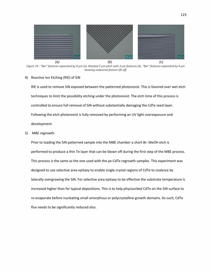
123
(a)
(b)
(c)
Figure 74 : “Bar” features separated by 8 μm (a). Rotated 5 μm pitch with 3 μm features (b). “Bar” features separated by 4 μm showing undesired feature lift-off.
4) Reactive Ion Etching (RIE) of SiN
RIE is used to remove SiN exposed between the patterned photoresist. This is favored over wet etch
techniques to limit the possibility etching under the photoresist. The etch time of this process is
controlled to ensure full removal of SiN without substantially damaging the CdTe seed layer.
Following the etch photoresist is fully removed by performing an UV light overexposure and
development.
5) MBE regrowth
Prior to loading the SiN patterned sample into the MBE chamber a short Br: MeOH etch is
performed to produce a thin Te layer that can be blown off during the first step of the MBE process.
This process is the same as the one used with the px-CdTe regrowth samples. This experiment was
designed to use selective area epitaxy to enable single crystal regions of CdTe to coalesce by
laterally overgrowing the SiN. For selective area epitaxy to be effective the substrate temperature is
increased higher than for typical depositions. This is to help physisorbed CdTe on the SiN surface to
re-evaporate before nucleating small amorphous or polycrystalline growth domains. As such, CdTe
flux needs to be significantly reduced also.

124
Figure 75: Optical images of single crystal CdTe seed layer surface (a) ; Patterned photoresist on SiN (b) ; and pseudo-px-CdTe deposited by MBE.
Using these methods 2 fully processed samples have been produced with the differing substrate
temperatures and CdTe deposition rates during epitaxial re-growth. Following deposition, these film are
characterized in a variety of ways. Full XRD FWHM and FTIR thickness mapping is completed after which
samples are further divided for various other measurements. Table 15 summarizes some of the full
wafer material properties.
Table 15: Pseudo-px-CdTe Samples summary
MBE Layer ID
MBE Growth Substrate
Temperature (°C)
MBE Layer Thickness {Average}
(μm)
Growth Rate (μm/hr)
XRD (422) DCRC FWHM
{Average ± Stdv} (Arcsec)
XRD (422) DCRC FWHM
{Min,Max} (Arcsec)
W13022 357 9.03 0.83 375 ± 159 162, -
W13023 365.9 2.6 0.61 325 ± 117 205, 740
These depositions were generally successful, however to achieve good selectivity, the growth rates
would have needed to be reduced by a factor of 10. As such there was still significant deposition of CdTe
on the SiN regions of the patterned substrate. Generally the deposition rate on the SiN was lower than
that of the exposed CdTe(211). The CdTe deposited on the SiN is polycrystalline, though in regions with
a small feature spacing, alternate epitaxial domains seem present. Full wafer analysis of these type of
samples is not as relevant as with other epitaxial samples because the SiN pattern is vastly different in
different regions of the 3” sample. It should be noted that sample W13022 was patterned at an angle of
approximately 3° between the primary <110> flat of the wafer and the horizontal axis of the mask. This

125
is indicated in Figure 76. The overall surface quality of W13023 was better than W13022 however. This
can be observed by the in the difference in overall darker color of the bulk of the wafer in the optical
scattering images found in Figure 76. This is due in part to the increased substrate temperature leading
to improved crystallinity, but also because of improved sample preparation.
Optical Scattering
Image
W13022
W13023
Thickness(μm)
Center =9.3 μm
Center = 11.91 μm
FWHM(Arcsec)
Average = 375”
Average = 325”
Figure 76: Pseudo-px-CdTe Samples Optical Scattering, FWHM and Thickness Mapping
Despite the less than perfect crystal quality it does seem as though a significant portion of the films have
maintained the (211) orientation even in the pseudo-px-CdTe regions. This is evident by the maintained
(422) peak associated with the primary orientation of the wafer. Due to the large number of features to
investigate with each of these samples only certain portions have been characterized in more detail.
First we consider sample (-20, 20) as indicated in Figure 76. Characterization of specific portions of this
sample is found in Figure 77. The 422 peak structure does indicate a significant amount of strain
~3°
(-20, 20)

126
present in the layers however, especially in the in the pseudo-px-CdTe regions. The attenuation of the
FTIR signal is also an indication of the difference in surface roughness of the pseudo polycrystalline
region compared to the mostly single crystalline region.
XRD (422)
FWHM >500 arcseconds
XRD (422)
FWHM = 170
FTIR
Thickness = 10.6
FTIR
Thickness = 12.3
Pseudo px-CdTe 10 μm pitch
7 μm features
Mostly sx-CdTe 10 boundaries with 8 μm spacing
Figure 77: This shows the approximate W13022 piece (-20,20) that was sent to NREL and indicates regions of pseudo px-CdTe (left) vs. mostly sx-CdTe (right). This is accompanied by XRD and FTIR data for these regions. The white block around each area is the boundary of the region and should have been SiN. A layer of nano-crystalline CdTe has been deposited here however. The orientation of the Si wafer is also shown. The <211> and <110> directions of the deposited CdTe layer should align with the Si wafer, though there is a tilt of the CdTe<211> orientation of ~3.8° with respect to the Si <211>.
Following analysis at UIC, 2PE-TRPL and EBSD were performed at NREL. The pseudo polycrystalline
region exhibited a lifetime of 0.3 ns while the primarily single crystalline region exhibited a 0.9 ns
lifetime. The difference in crystallinity or sample thickness does not directly explain this result, however
enhanced surface recombination might. If we assume that in addition to the top surface and bottom
interface there are also the surfaces between the small nucleated regions, surface recombination may
be significant at these interfaces also. Assuming that the contributions from the different feature
dimensions will affect the measured life time in a way similar to the combination of surface related vs.
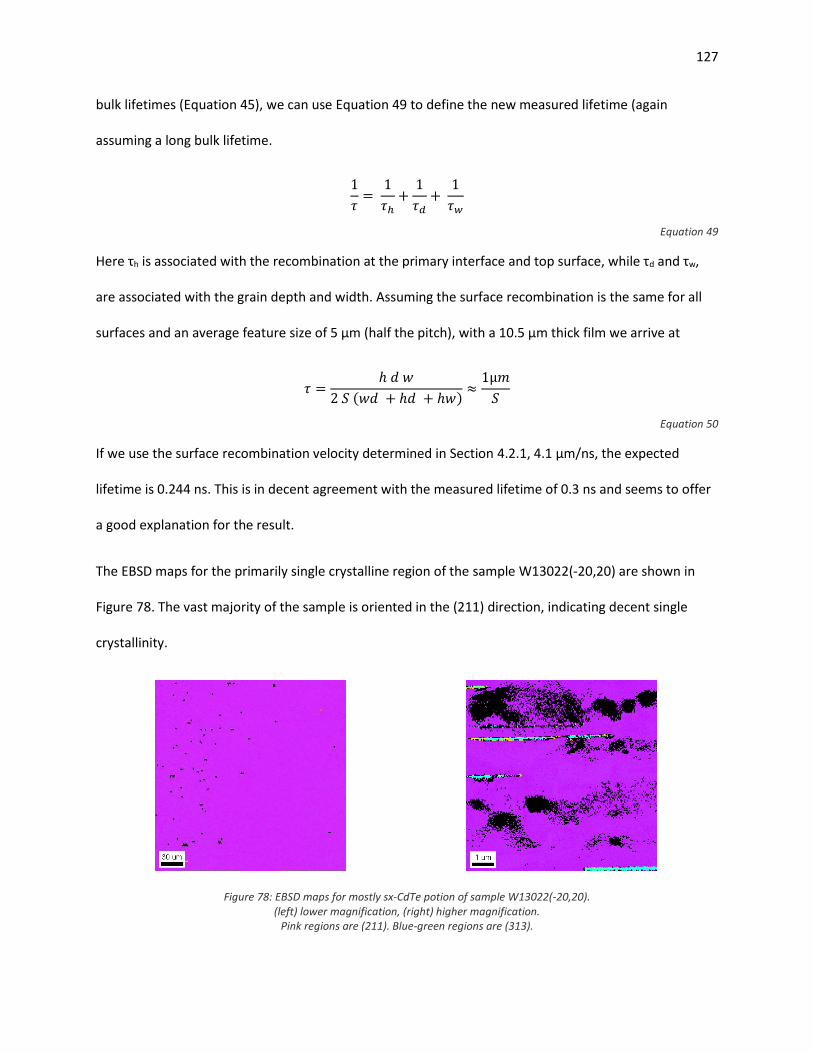
127
bulk lifetimes (Equation 45), we can use Equation 49 to define the new measured lifetime (again
assuming a long bulk lifetime.
1
𝜏=
1
𝜏ℎ+
1
𝜏𝑑+
1
𝜏𝑤
Equation 49
Here τh is associated with the recombination at the primary interface and top surface, while τd and τw,
are associated with the grain depth and width. Assuming the surface recombination is the same for all
surfaces and an average feature size of 5 µm (half the pitch), with a 10.5 µm thick film we arrive at
𝜏 =ℎ 𝑑 𝑤
2 𝑆 (𝑤𝑑 + ℎ𝑑 + ℎ𝑤)≈
1µ𝑚
𝑆
Equation 50
If we use the surface recombination velocity determined in Section 4.2.1, 4.1 µm/ns, the expected
lifetime is 0.244 ns. This is in decent agreement with the measured lifetime of 0.3 ns and seems to offer
a good explanation for the result.
The EBSD maps for the primarily single crystalline region of the sample W13022(-20,20) are shown in
Figure 78. The vast majority of the sample is oriented in the (211) direction, indicating decent single
crystallinity.
Figure 78: EBSD maps for mostly sx-CdTe potion of sample W13022(-20,20). (left) lower magnification, (right) higher magnification.
Pink regions are (211). Blue-green regions are (313).

128
The pseudo-px-CdTe region EBSD maps are shown in Figure 79. It is clear from these images that there
are two primary growth domains present, (211) and (313). The (313) orientation is a twin of the (211)
orientation and as such the boundaries between these domains form CSL Σ3 grain boundaries. This type
of boundary is common in the bulk of typical px-CdTe grains. The EBSD scan also shows the highly
ordered nature of the boundaries in this region, though features are elongated in a (110) direction. This
can may explained due to the step flow growth mode of CdTe(211). The 211 orientation is terraced by
(100) and (111) oriented faces. The sticking coefficient for (111) face is greater than that of the (100)
face and as such epitaxial growth tends to progress as the step of (111) growth faces flows across the
surface of the sample. The elongated features in the (110) direction are an indication of this terraced
growth. It has also been previously shown that at higher growth temperature, the (313) orientation twin
is more likely to form [75]. This couples with the stain due to lateral overgrowth of the SiN features
would explain the presence of these two orientation.
Figure 79: EBSD maps for pseudo-px-CdTe portion of sample W13022(-20,20).
(left) lower magnification, (right) higher magnification. Pink regions are (211). Blue-green regions are (313).
Due to the elongation of features in the (110) direction we can modify the previous estimation of the
lifetime by assuming closer to 10 µm grain depth as evident in Figure 79. Using this assumption, the
estimated recombination lifetime is 0.31 ns, which is in excellent agreement with the measured lifetime.
The surface characteristics of sample W13023 have been analyzed using AFM. Figure 80 shows a direct
comparison of CSS px-CdTe sample compared to the pseudo-px-CdTe sample W13023. The highly order
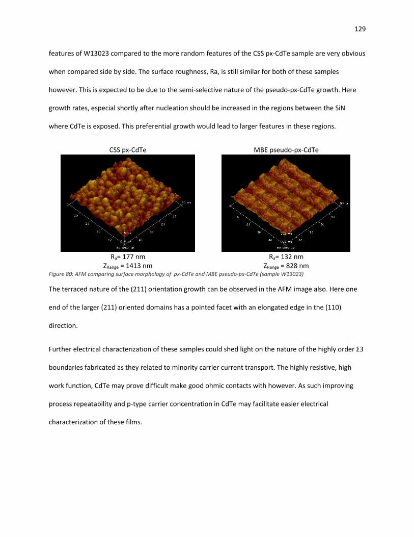
129
features of W13023 compared to the more random features of the CSS px-CdTe sample are very obvious
when compared side by side. The surface roughness, Ra, is still similar for both of these samples
however. This is expected to be due to the semi-selective nature of the pseudo-px-CdTe growth. Here
growth rates, especial shortly after nucleation should be increased in the regions between the SiN
where CdTe is exposed. This preferential growth would lead to larger features in these regions.
CSS px-CdTe
Ra= 177 nm
ZRange = 1413 nm
MBE pseudo-px-CdTe
Ra= 132 nm
ZRange = 828 nm Figure 80: AFM comparing surface morphology of px-CdTe and MBE pseudo-px-CdTe (sample W13023)
The terraced nature of the (211) orientation growth can be observed in the AFM image also. Here one
end of the larger (211) oriented domains has a pointed facet with an elongated edge in the (110)
direction.
Further electrical characterization of these samples could shed light on the nature of the highly order Σ3
boundaries fabricated as they related to minority carrier current transport. The highly resistive, high
work function, CdTe may prove difficult make good ohmic contacts with however. As such improving
process repeatability and p-type carrier concentration in CdTe may facilitate easier electrical
characterization of these films.

130
5.3 DISCUSSION
Regarding to the development of methods to fabricate polycrystalline CdTe material in controlled ways
using MBE, this project can be considered a success. Highly polycrystalline (CSL, non-CSL, high- and low-
angle boundaries) regrowth is shown to allow for CSS like material to be deposited in the controlled
environment of an MBE system, while pseudo-px-CdTe growth using semi-selective area epitaxy on
patterned substrates has been shown to produce to CSL Σ3 boundaries in a controllable way. That said,
the samples produced as part of this project have only begun to represent the possible types of samples
that could be fabricated using these methods. Adjustment of stoichiometry during deposition, and or
doping are simple examples that wouldn’t even constitute substantially different structural properties.
More complete analysis of samples that can be fabricated in these ways will certainly be beneficial,
though it will require substantial effort. It is unclear, given this data set weather non CSL grain
boundaries can be fabricated using the pseudo-px deposition methods examined. Adjustment of
substrate orientation or type, improved selectivity, or adjusted growth conditions may allow for this
however. The large amount of processing necessary for fabrication of these types of films is a drawback
to the method, as it drastically increases the time to fabricate samples in addition to increasing the
number of potential reasons for a particular inconsistency in data. In this way, it mimics the some of the
issues associated with thin-film CdTe device characterization in general. That said, additional deposition
attempts, and further characterization would be beneficial to truly asses the viability of the method.

131
6 CONCLUSIONS
Through standard device optimization processes using the typical superstrate device configuration, thin
film px-CdTe solar photovoltaic cells of greater than 15% efficiency have been produced on
commercially available TCO coated glass. The performance limitations of these devices represent well
the standard drawbacks to the typical device structure and fabrication methods. Initial characterization
by STEM reveals a wide variety of potential minority carrier transport limiting defects in px-CdTe, both in
the form of non-CSL boundaries of independently nucleated grains and along with dislocation and
extended CSL boundaries within the bulk of the grains themselves. As a means to study more
fundamental material properties, investigation of CdTe layers deposited by MBE has been carried out.
2PE-TRPL lifetimes in thin (less than 20 µm) hetero-epitaxial CdTe layers are shown to be highly surface
recombination dominated. 2PE-TRPL lifetimes are correlated with crystal quality (422 peak FWHM) also.
Despite the relationship of crystal quality to defect density, this correlation is expected to be
coincidental considering that annihilation of dislocations, and as such improved crystal quality, can also
be correlated to the thickness of the epitaxial film. Additional Te overpressure during epitaxial growth is
shown to improve layer uniformity and crystal quality, especially for thinner (less than 10 µm) CdTe
layers. The exact reasons for the improvements are not yet fully understood though it is likely associated
with maintained surface quality throughout deposition preventing formation of new dislocation. P-type
CdTe films doped using arsenic from two different material sources, Cd3As2 effusion and As cracker,
have exhibited carrier concentrations in the 1015 cm-3 range. Though higher carrier concentration have
been achieved using the arsenic cracker, reduced crystal quality and activation percentage may limit its
viability.
Polycrystalline CdTe has been deposited using MBE by two different methods, regrowth on CSS
deposited px-CdTe, and pseudo-px deposition using semi-selective area epitaxy on patterned substrates.
131

132
The highly polycrystalline material using the regrowth method may be more relevant to the highly
polycrystalline material currently produced using high throughput processing techniques, though the
pseudo-px deposition methods has the advantage of isolating a particular type of extended defect.
MBE is shown to be a viable method for investigation of many aspects of current CdTe material for solar
photovoltaic applications and future investigations taking advantage of these methods may allow for
significantly enhanced device performance as well as improved understanding of overall performance
limitations of this complex material system.

133
APPENDIX A – BICRYSTAL REGROWTH
This section is meant to summarize the results of the work done as part of the DOE Bridge project with
regard to regrowth on CdTe bi-crystals.
Work for the past year has focused on two preliminary aspects of depositing highly doped single crystal
(sx-) CdTe on CdTe bi-crystals fabricated at the University of Texas Dallas (UTD). Those two aspects are
(1) deposition of sx-CdTe on CdTe(110) bulk substrates (2) deposition of highly p-type CdTe (See Section
4.2.3.2). While progress for the second area has progressed substantially, the substrates and <110>
orientation have proven difficult to reliably re-deposition sx-CdTe on the bulk substrate. Details of this
work are presented in the following sections.
Deposition of sx-CdTe on CdTe<110> Bulk
MPL is currently using a RIBER Opus 45 system for solar photovoltaic related CdTe depositions. Our
typical process involves heteroepitaxy of CdTe(211)B on 3 inch Si(211) wafers. The process for regrowth
of CdTe on bulk CdTe substrates is different in sample preparation, the sample holder and mounting
techniques used, and the typical growth recipe. The process developed for bulk single crystal regrowth is
diagramed in Figure 81.
Figure 81: Standard MBE CdTe regrowth process.
The Br:MeOH etch produces a Te rich surface that can be desorbed in a higher temperature step prior to
CdTe deposition in order to expose a clean CdTe surface. Br:MeOH is a fairly common polishing etch and
as such the mirror-like surface quality should be maintained or improved with etching. It is also
Sample Prep Dilute (~0.5%) Br:MeOH etch
MeOH and DI rinse and dry
DAG mount to molybdenum block holder
Load and Pump Chamber
Growth RecipePre-Bake
Ramp to ~200°C and hold
Te desporb
Ramp to >350°C
Wait for RHEED transition
Growth
Return to 300°C
~1µm/hr
CharacterizationVisual
Surface should be "mirror-like"
XRD
CdTe(422) DCRC
Crystal Quality
Hall
Electrical properties
133

134
important to have the growth system, with specific holders and substrates, properly calibrated so that
actual surface temperature is known for a given set-point temperature. The first regrowth attempt,
W13022, is considered a failure as a result of mistakes associated with these two aspects of re-growth.
The Br:MeOH etch visibly disturbed the surface, changing from a smooth to matt surface after etching
and the set-points used were calibrated for the standard 3 inch Si sample holder. The sample size and
location prevented RHEED observation throughout the deposition also. Figure 82 shows the CdTe(422)
rocking curve scans for the sample before and after deposition. Peak strength is diminished substantially
and along with it the FWHM.
Figure 82: Before (Green) and after (Red) XRD DCRC scans for sample W13022 CdTe(110) re-growth
After recalibration of the surface to set-point temperature several CdTe on CdTe(211)/Si(211) re-growth
attempts resulted in maintained surface quality and improved FWHM crystal quality characteristics. A
second CdTe(110) growth attempt resulted poor crystal quality also however. For this deposition the
surface quality during the etch was initially similar to the first sample, visibly rough. Allowing the etch to
progress for a longer time allowed the surface quality to be restored however. A larger
CdTe(211)/Si(211) sample was also loaded in order to allow for clean observation of RHEED transitions.
Despite the improved surface preparation and calibrated growth recipe, the resulting deposition
exhibited a mostly matt surface quality. Small portions of the sample were mirror-like, but the majority
was not. The reason for this deposition failure may be associated with the substrate orientation chosen.
CdTe(211) growth is known to progress in a step-flow growth where the (100) face grows slightly faster

135
than the (111) face tending to repress twining. The CdTe (110) surface on the other hand is highly
symmetric, and competing (111) growth faces result in twining (see Figure 83). Despite this discouraging
result it is suspected that high quality CdTe regrowth of (211) oriented bulk substrates will be possible
and repeatable.
Figure 83: Comparison of CdTe(211) {left} and CdTe(011) {right} surface with (111) and (100) growth orientations identified

136
REFERENCES
[1] J. Loferski, Journal of Applied Physics, vol. 27, pp. 777-784, 1956.
[2] P. Rappaport, RCA Review, vol. 20, pp. 373-397, 1959.
[3] W. Shockley and H. Queisser, " Detailed Balance Limit of Efficiency of p-n Junction Solar Cells,"
Journal of Applied Physics, vol. 32, pp. 510-519, 1961.
[4] K. Mitchell, A. Fahrenbruch and R. Bube, Journal of Applied Physics, vol. 48, pp. 829-830, 1977.
[5] K. Yamaguchi, H. Masumoto, N. Nakayama and S. Ikegami, "Japanese Journal of Applied Physics,"
vol. 16, pp. 1203-1211, 1977.
[6] J. Britt and C. Ferekides, Applied Physics Letters, vol. 62, pp. 2851-2852, 1993.
[7] X. Wu, Journal of Applied Physics, vol. 89, pp. 4564-4569, 2001.
[8] P. (. Maycock, Photovoltaic News, Feb 2001.
[9] M. Kanellos and B. Prior, "Are Solar Thermal Power Plants Doomed?," 2010. [Online]. Available:
https://www.greentechmedia.com/articles/read/is-CSP-doomed/.
[10] R. Banai, C. Blissett, E. Colegrove and C. Gilmore, "Polycrystalline CdTe Solar Cells on Buffered
Commercial TCO-Coated Glass with Efficiencies above 15%," in 37th IEEE Photovoltaic Specialist
Conference, Seattle, WA, 2011.
[11] E. Colegrove, R. Banai, C. Blissett, C. Burma, J. Ellsworth, M. Morley, S. Barnes, C. Gilmore, J.
Bergenson, R. Dhere, M. Scott, T. Gessert and S. Sivananthan, "High-Efficiency Polycrystalline
CdS/CdTe Solar Cells on Buffered Commercial TCO-coated Glass," Journal of Electronic Materials,
vol. 41, no. 10, 2012.
[12] Z. Fang, X. Wang, H. Wu and C. Zhao, "Achievements and Challenges of CdS/CdTe Solar Cells,"
International Journal of Photenergy, 2011.
[13] M. Green, "Solar Cell Efficiency Tables," Progress in Photovoltaics, vol. 22, no. 1, 2013.
[14] M. Green, "Solar Cell Efficiency Tables (version 36)," Progress in Photovoltaics, vol. 18, no. 5, 2010.
[15] M. Green, "Solar Cell Efficiency Tables (version 39)," Progress in Photovoltaics, vol. 20, no. 1, 2011.
[16] M. Green, "Solar Cell Efficiency Tables (version 41)," Progress in Photovoltaics, vol. 21, no. 1, 2012.
[17] A. Kanevce and T. Gessert, "Optimizing CdTe Solar Cell Performance: Impact of variations in
Minority-Carrier Lifetime and Carrier Density Profile," Journal of Photovoltaics, vol. 1, no. 1, 2011.
136

137
[18] J. Sites, J. Granata and J. Hiltner, "Losses due to polycrystallinity in thin-film solar cells," Solar
Energy Materials and Solar Cells, vol. 55, pp. 43-50, 1998.
[19] A. Romeo, D. Batzner, H. Zogg and A. Tiwari, "Recrystallization in CdTe/CdS," Thin Solid Films, Vols.
361-362, pp. 420-425, 2000.
[20] R. Chakrabarti, J. Dutta, S. Bandyopadhyay, D. Bhattacharyya, S. Chaudhuri and A. Pal, "Surface
photovoltage measurement in CdS/CdTe solar cell: Grain boundary effect," Solar Energy Materials
and Solar Cells, vol. 61, no. 2, pp. 113-126, 2000.
[21] K. Durose, M. Cousins, D. Boyle, J. Beier and D. Bonnet, "Grain boundaries and impurities in
CdTe/CdS solar cells," Thin Solid Films, Vols. 403-404, pp. 396-404, 2002.
[22] W. Metzger and M. Gloeckler, "The impact of charged grain boundaries on thin-film solar cells and
characterization," Journal of Applied Physics, vol. 98, no. 6, 2005.
[23] I. Visoly-Fisher, S. Cohen, K. Gartsman, A. Ruzin and D. Cahen, "Understanding the Beneficial Role
of Grain Boundaries in Polycrystalline Solar Cells from Single-Grain-Boundary Scanning Probe
Microscopy," Advanced Functional Materials, vol. 16, no. 5, pp. 649-660, 2006.
[24] K. Suzuki and H. Shiraki, "Evaluation of Surface Recombination Velocity on CdTe Radiation
Detectors by Time-of-Flight Measurements," IEEE Transactions on Nuclear Science, vol. 56, no. 4,
pp. 1712-1716, 2009.
[25] F. Troni, R. Menozzi, E. Colegrove and C. Buurma, "Simulation of Current Transport in
Polycrystalline CdTe Solar Cells," Journal of Electronic Materials , vol. 42, no. 11, pp. 3175-3180,
2013.
[26] J. Nelson, The Physics of Solar Cells, London: Imperial College Press, 2004.
[27] A. (. Luque and S. (. Hegedus, Handbook of Photovoltaic Science and Engineering 2nd Ed., John
Wiley & Sons, Ltd, 2011.
[28] N. Ashcroft and N. Mermin, Solid State Physics, Cengage Learning, 1976.
[29] Kittel, Introduction to Solid State Physics (8th Ed), Wiley, 2004.
[30] E. Ghahramani, D. Moss and J. Sipe, "Full-band-structure calculations of first-,second-, and third-
harmonic optical response coefficients of ZnSe, ZnTe, and CdTe," Physical Review B, vol. 43, no. 12,
pp. 9700-9710, 1991.
[31] "p-n junction diagram," [Online]. Available: http://en.wikipedia.org/wiki/File:Pn-junction-
equilibrium-graphs.png.
[32] "Solar Spectrum Plot," [Online]. Available: http://www.pveducation.org/pvcdrom/properties-of-
sunlight/atmospheric-effects.

138
[33] "Shockley-Queisser Limit Plots," [Online]. Available: http://en.wikipedia.org/wiki/Shockley-
Queisser_limit.
[34] "Mobile Power Technology: AltaDevices," 2013. [Online]. Available:
http://www.altadevices.com/technology-overview.php.
[35] B. McCandless, J. Sites, A. (. Luque and S. (. Hegedus, "Chapter 14 - Cadmium Telluride Solar Cells,"
in Handbook of Photovoltaic Science and Engineering 2nd Edition, John Wiley & Sons, Ltd, 2011,
pp. 600-641.
[36] J. Cruz-Campa and D. Zubia, "CdTe thin film growth model under CSS conditions," Solar Energy
Materials & Solar Cells, vol. 93, pp. 15-18, 2009.
[37] ASM Binary Phase Diagrams, 2000.
[38] R. Behrisch, Sputtering by Particle Bombardment, Berlin: Springer, 1981.
[39] G. Green, " On the motion of waves in a variable canal of small depth and width," Transactions of
the Cambridge Philosophical Society, vol. 6, pp. 457-462, 1837.
[40] H. Jeffreys, "On certain approximate solutions of linear differential equations of the second order,"
Proceedings of the London Mathematical Society, vol. 23, pp. 428-436, 1924.
[41] E. Hecht, Optics (2nd ed), Addison Wesley, 1987.
[42] M. Born and E. Wolf, Principles of optics: electromagnetic theory of propagation, interference and
diffraction of light., Oxford Pergamon Press, 1964.
[43] J. Lambert, On the measure and gradients of light, colors, and shade., Augsburg, Germany:
Eberhardt Klett, 1760.
[44] "Chapter 3," in Optical Processes in Semiconductors, New York, NY, Dover Publications, 1971, pp.
34-81.
[45] "Thin film interference diagram," [Online]. Available:
http://upload.wikimedia.org/wikipedia/commons/0/01/Thin_film_interference1.gif.
[46] "CdTe index vs wavelength," [Online]. Available:
http://www.reading.ac.uk/infrared/library/infraredmaterials/ir-infraredmaterials-cdte.aspx .
[47] "Integrating Sphere Diagram," [Online]. Available: http://www.zae.uni-
wuerzburg.de/files/ulbricht3_e.gif.
[48] J. Williamson, Processng Instrumentation for Intustrial Engineering, vol. 182, no. 21, 1967.
[49] R. Young, J. Ward and F. Scire, IEEE Review of Scientific Intruments, vol. 43, no. 7, 1972.
[50] K. Levenberg, Questions in Applied Mathematics , vol. 2, p. 164, 1944.

139
[51] D. Marquardt, SIAM Journal of Applied Mathematics, vol. 11, p. 431, 1963.
[52] O. Semonin, J. Luther, S. Choi, H.-Y. Chen, J. Gao, A. Nozik and M. Beard, "Peak External
Photocurrent Quatum Efficiency Exceeding 100% via MEG in a Quantum Dot Solar Cell," Science,
vol. 334, 2011.
[53] S. Demtsu and J. Sites, "Quantification of Losses in CdTe Solar Cells," in IEEE Photovoltaic
Specialists Conference, 2005.
[54] A. Crew, M. Isaacson and D. Johnson, "A Simple Scanning Electron Microscope," Review of
Scientific Instrumentation, vol. 40, p. 241, 1969.
[55] A. Crewe, J. Wall and J. Langmore, "Visibility of Single Atoms," Science, vol. 168, 1970.
[56] "STEM Diagram," [Online]. Available:
http://www.nature.com/nmat/journal/v8/n4/fig_tab/nmat2380_F3.html.
[57] E. Rutherford and F.R.S., "The scattering of alpha and beta paricles by matter and the sctructure of
the atom," Philosophical Magize, vol. 21, no. 6, pp. 669-688, 1911.
[58] X. Wu, P. Sheldon, Y. Mahathongdy, R. Ribelin, A. Mason, H. Moutinho and T. Coutts, in
Proceedings of 15th NREL/SNL PV Program Review Meeting, Denver, CO, 1998.
[59] X. Li, R. Ribelin, Y. Mahathongdy, D. Albin, R. Dhere, D. Rose, S. Asher, H. Moutinho and P. Sheldon,
in Proceedings of the 15th NREL/SNL PV Program Review Meeting, Denver, CO, 1998.
[60] C. Ferekides, R. Mamazza, U. Balasubramanian and D. Morel, Thin Solid Films, vol. 224, pp. 480-
481, 2005.
[61] A. Gupta, V. Parikh and A. Compaan, Solar Engery and Materials for Solar Cells, vol. 90, p. 2263,
2006.
[62] N. Romeo, A. C. V. Bosio and A. Podesta, Solar Energy, vol. 77, p. 795, 2004.
[63] R. F. Klie, T. Paulauskas, R. Tao, E. Colegrove, C. Gilmore, C. Blissett, S. Sivananthan and R. Dhere,
"Atomic Resolution Characterization of Polycrystalline CdTE Solar Cell Devices," in International
Syposium on Optoelectronic Materials, Chicago, 2012.
[64] E. Colegrove, Z. Guo, R. Klie, S. Sivananthan, W. B. C. Gao, R. Dhere and T. Gessert, "STEM
Characterization of polycrystalline CdS/CdTe solar devices," in MRS Spring Meeting, San Francisco,
CA, 2013.
[65] C. Li, J. Poplawsky, Y. Wu, A. Lupini, A. Mouti, D. Leonard, N. Paudel, K. Jones, W. Yin, M. Al-Jassim,
Y. Yan and S. Pennycook, "From atomic structure to photovoltaic properties in CdTe solar cells,"
Ultramicroscopy, vol. 134, pp. 113-125, 2013.

140
[66] A. Cho and J. Arthur, "Molecular Beam Epitaxy," Progress in Solid State Chemistry, vol. 10, pp. 157-
192, 1975.
[67] M. Herman and H. Sitter, Molecular Beam Epitaxy: Fundementals and Current Status, Springer-
Verlag, 1988.
[68] J. Faurie, "Molecular Beam Epitaxy of HgCdTe: Growth And Characterization," Progress in Crystal
Growth and Characterization, vol. 29, pp. 85-159, 1994.
[69] J. Garland and S. Sivananthan, "Molecular Beam Epitaxial Growth of HgCdTe," in Handbook of
Crystal Growth, Springer Berlin Heidelberg, 2010, pp. 1069-1132.
[70] "Epitaxial Surface Dynamics," [Online]. Available: http://www.physik.uni-
kl.de/hillebrands/research/methods/molecular-beam-epitaxy/.
[71] "Epitaxial Growth Regimes," [Online]. Available:
http://en.wikipedia.org/wiki/Stranski%E2%80%93Krastanov_growth.
[72] A. Chambers, Modern Vacuum Physics, Boca Raton: Chapman and Hall/CRC, 2005.
[73] S. Fahey, Selective Area Epitaxy of CdTe on Nanopatterned Substrates, Chicago: Univeristy of
Illinois at Chicago (Thesis), 2012.
[74] "Zinc-Blende Structure," [Online]. Available:
http://chemistry.osu.edu/~woodward/ch754/struct/ZnS.htm.
[75] S. Rujirawat, The CdTe/Si(111):As Interface, Chicago, IL: Univeristy of Illinois at Chicago (Thesis),
2000.
[76] R. Koestner and H. Schaake, Journal of Vacuum Science and Technology A, vol. 6, no. 4, pp. 2834-
2839, 1988.
[77] S. Sivananthan, X. Chu, J. Reno and J. Faurie, Journal of Applied Physics, vol. 60, no. 4, pp. 1359-
1363, 1986.
[78] W. P. D. Kern, RCA Review, vol. 31, no. 187, 1970.
[79] D. Murphy, "Differential interference contrast (DIC) microscopy and modulation contrast
microscopy," in Fundementals of Light Microscopy and Digital Imaging, New York, NY, Wiley-Liss,
2001, pp. 153-168.
[80] P. Fellgett, Univeisty of Cambridge (Thesis), 1951.
[81] J. Ayers, Jounral of Crystal Growth, vol. 135, pp. 71-77, 1994.

141
[82] W. Metzger, D. Albin, D. Levi, P. Sheldon, X. Li, B. Keyes and R. Ahrenkiel, "Time-Resolved
Photoluminescence Studies of CdTe Solar Cells," Journal of Applied Physics, vol. 94, no. 5, pp. 3549-
3555, 2003.
[83] A. Kanevce, D. Kuciauskas, T. A. Gessert, D. Levi and D. Albin, "Impact of Interface Recombination
on TRPL decays in CdTe solar cells (Numerical simulation analysis)," in 38th IEEE Photovoltaic
Specialists Conference, Austin, TX, 2012.
[84] D. Kuciauskas, A. Kanevce, J. Burst, J. Duenow, R. Dhere, D. Albin, D. Levi and R. Ahrenkiel,
"Minority Carrier Lifetime Analysis in the Bulk of Thin-Film Absorbers Using Subbandgap (Two-
Photon) Excitation," IEEE Journal of Photovoltaics, vol. 3, no. 4, pp. 1319-1324, 2013.
[85] E. Hall, " On a New Action of the Magnet on Electric Currents," American Journal of Mathematics,
vol. 2, no. 3, pp. 287-292, 1879.
[86] S. Wei and A. Zunger, "Calculated natural band offsets of all II-VI and II-V semiconductors:
Chemical trends and the role of cation d orbitals," Applied Physics Letters, vol. 72, 1998.
[87] C. Lennon, L. Almeida, R. Jacobs, J. Benson, P. Smith, J. Markunas, J. Arias and J. Pellegrino, "The
Surface Kinetics of MBE-Grown CdTE(211)B During In Situ Cyclic Annealing," Journal of Electronic
Materials, vol. 42, no. 11, pp. 3344-3348, 2013.
[88] S. Wei and S. Zhang, "Chemical trends of defect formation and doping limit in II-VI semiconductors:
The case of CdTe," Physical Review B, vol. 66, 2002.
[89] R. Kodama, T. Seldrum, X. Wang, J. Park, E. Colegrove, X. Zheng, R. Dhere and S. Sivananthan,
"Nitrogen plasma doping of single crystal ZnTe and CdZnTe on Si by MBE," Jounral of Electronic
Materials, vol. 42, no. 11, 2013.
[90] T. Baron, S. Tatarenko, K. Saminadayar, N. Magnea and J. fontenille, "Plasma Nitrogen doping of
ZnTe, CdZnTe, and CdTe by molecular beam epitaxy," Applied Physics Letters , vol. 65, 1994.
[91] T. Baron, K. Saminadaya and N. Magnea, "Nitrogen doping of tellurium-based II-VI compounds
during growth by molecular beam epitaxy," Applied Physics Letters, vol. 67, no. 20, 1995.
[92] T. Baron, K. Saminadayar and N. Magnea, "Nitrogen doping of Te-base II-VI compounds during
growth by molecular beam epitaxy," Journal of Applied Physics, vol. 83, no. 3, 1998.
[93] X. Dong, T. Biegala, M. Carmody, J. Garland, C. Grein and S. Sivananthan, "Proposed monolithic
triple-junction solar cell structures with the potential for ultrahigh efficiencies using II-VI alloys and
silicon substrates," Applied Physics Letters, vol. 96, 2010.
[94] J. Park, S. Farrell, C. Blissett, X. Wang, E. Colegrove, W. Metzger, T. Gessert and S. Sivananthan,
"Incorporation and activation of arsenic dopant in single crystal CdTe on Si," in The US Workshop
on the Physics and Chemistry of II-VI Materials, Chicago, IL, 2013.

142
[95] J. Westmore, K. Mann and A. Tickner, "Mass Spectrometric Study of Nonstoichiometric
Vaporization of Cadmium Arsenide," Journal of Physical Chemistry, pp. 606-612, 1965.
[96] H. Moutinho, M. Romero, J. Moseley, R. Dhere, C.-S. Jiang, K. Jones, J. Duenow and M. Al-Jassim,
"Structural and Electro-Optical Properties of CdTe Films Used in CdTe/CdS Solar Cells Grown with
Superstrate Configuration," in MRS Fall Meeting, Boston, 2012.
[97] B. McCandless, I. Youm and R. Birkmire, "Optimization of Vapor Post-deposition Processing for
Evaporated CdS/CdTe Solar Cells," Progress in Photovoltaics: Research and Applications , vol. 7, pp.
21-30, 1999.
[98] A. Romeo, S. Buecheler, M. Giarla, G. Mariotto, A. Tiwari, A. Bosio and S. Mazzamuto, "Study of
CSS- and HVE-CdTe by different recrystallization processes," Thin Solid Films, vol. 517, pp. 2132-
2135, 2009.
[99] R. Jaeger, "Lithography," in Introduction to Microelectronic Fabricaton (2nd ed.), Upper Saddle
River, Prentice Hall, 2002.

143
VITA
Eric Colegrove
Education Ph.D. Physics University of Illinois at Chicago (UIC) Chicago, IL 60607 May 2014
B.S. Physics, Minor Math and Philosophy Hamline University Saint Paul, MN 55104 May 2009 : Magna Cum-Laude with Honors
Graduate Research and Industry Experience Fall 2012-Present
Research Assistant UIC Microphysics Lab: Solar Team Thesis: “Fundamental Investigations of CdTe deposited by MBE for applications in thin film CdTe photovoltaics” MBE CdTe on Si, CdTe, process optimization, film characterization o NREL Subcontract “Research and Development of MBE CdTe” o DOE Bridge Program “ How grain boundaries affect the efficiency of poly-
CdTe solar-cells” Fall 2011-2012
Photovoltaics and MBE Engineer EPIR Technologies, Inc.: CdTe Solar PV CSS for polycrystalline CdTe photovoltaics - Process optimization and characterization o Internship Project Manager/Collaborator Trainer: Developed and led CSS
training projects MBE CdTe on Si - System installation, process optimization, maintenance,
characterization Summer 2010, 2011
Photovoltaics Internships EPIR Technologies, Inc.: Poly-CdTe PV Team Development of >15% efficient polycrystalline CdS/CdTe solar cells o Chemical Bath Deposition (CBD), back contact annealing, and J-V analysis
Funding proposal, internal publication, and presentation writing, editing, and review
Teaching 2009- 2012
Teaching Assistantship UIC Physics Dept.: Intro. to Physics II Coordinator: Manage TAs, write syllabus, manage grades, maintain website Discussion Lead: develop assignments, manage class time, grade assignments
Technical Skills Fabrication: MBE, CSS, CBD, Wet Bench/Hood, Tube furnace,
photolithography, Sputtering Characterization: XRD, FTIR, RHEED, Hall, Spectrophotometery, J-V analysis,
SEM, EDS, XPS Computer Skills: M.S. Office, JMP, Mathematica, Labview, C++
143

144
Awards and Honors Phi Beta Kappa, Eagle Scout
Activities and Outreach Leadership: InSPIRE Student Org. (UIC) - Founding Member /Treasurer(’13)
SPS (Hamline) - President(’09) Hobbies: Soccer, Sailing, Cello, Camping
Publications In Print
1. R. Kodama, T. Seldrum, X. Wang, J.H. Park, E. Colegrove, X. Zheng, R. Dhere, and
S. Sivananthan, “Nitrogen plasma doping of Single Crystal ZnTe and CdZnTe on Si by
MBE,” Journal of Electronic Materials, Vol. 42, No. 11, 2013
2. F. Troni, R. Menozzi, E. Colegrove, and C. Buurma, “Simulation of Current Transport
in Polycrystalline CdTe Solar Cells,” Journal of Electronic Materials, Vol. 42, No. 11,
2013
3. E. Colegrove, R. Banai, C. Blissett, C. Buurma, J. Ellsworth, M. Morley, S. Barnes, C.
Gilmore, J. Bergeson, R. Dhere, M. Scott, T. Gessert and Siva Sivananthan, “High-
Efficiency Polycrystalline CdS/CdTe Solar Cells on Buffered Commercial TCO-Coated
Glass,” Journal of Electronic Materials, Vol. 41, No. 10, 2012
4. R. Banai, C. Blissett, C. Buurma, E. Colegrove, C. Gilmore, et al., “Polycrystalline
CdTe Solar Cells on Buffered Commercial TCO-Coated Glass with Efficiencies above
15%”, 37th IEEE Photovoltaic
Specialist Conference, 2011
Submitted 1. M. Thanihaichelvan, P. Ravirajan, K. Balashanga, GDK Mahanama, L. Dissanayake,
E. Colegrove, R. Dhere, and S. Sivananthan, “Effect of surface roughness of the substrate on the performance of polycrystalline CdS/CdTe solar cells,” Journal of Electronic Materials
Conference and Workshop Presentations * = Presented
1. “Overview of II-VI based solar cells,” *E. Colegrove, R. Dhere, and S. Sivananthan, 2013 International Conference and Exhibition on Lasers, Optics & Photonics – (San Antonio, TX)
2. “MBE polycrystalline CdTe for controlled grain boundary analysis,” *E. Colegrove, B. Stafford, S. Parkhurst, W. Gao, T. Gessert, and S. Sivananthan, 2013 II-VI Workshop – (Chicago, IL)
3. “Effect of surface roughness of the substrate on the performance of polycrystalline CdS/CdTe solar cells,” M. Thanihaichelvan, P. Ravirajan, *K. Balashanga, GDK Mahanama, L. Dissanayake, E. Colegrove, R. Dhere, and S. Sivananthan, 2013 II-VI Workshop – (Chicago, IL)
4. “STEM characterization of polycrystalline CdS/CdTe solar devices,” *E. Colegrove, Z. Guo, R. Klie, S. Sivananthan, W. Gao, C. Blissett, R. Dhere, T. Gessert , 2013 MRS Spring Meeting – (San Francisco, CA)
145
5. “Nitrogen plasma doping of Single Crystal ZnTe and CdZnTe on Si by MBE,” R. Kodama, T. Seldrum, X. Wang, J.H. Park, *E. Colegrove, X. Zheng, R. Dhere, and S. Sivananthan, 2012 II-VI Workshop – (Seattle, WA)
6. “High efficiency polycrystalline CdS/CdTe solar cells on buffered commercial TCO-coated glass,” *E. Colegrove, R. Banai, C. Blissett, C. Buurma, J. Ellsworth, M. Morley, S. Barnes, C. Gilmore, J. Bergeson, R. Dhere, M. Scott, T. Gessert and Siva Sivananthan, 2011 II-VI Workshop – (Chicago, IL)
7. “Effects of Buffer Layer and thickness of window-layer on performance of Highly Efficient Polycrystalline Cadmium Sulfide(CdS)/Cadmium Telluride (CdTe) Solar cells” , *M Thanihaichelvan, P. Ravirajan, GDK Mahanama, MAKL. Dissanayake, E. Colegrove, R. Dhere, and S. Sivananthan- 2013 International Conference on New and Renewable Energy -– (Daegu, Korea)
8. “Effect of CdTe layer thickness on the properties of CdS/CdTe solar cells,” *G.D.K.Mahanama, P.Ravirajan, E. Colegrove, M.A.K.L.Dissanayake, R.Dhere, and S.Sivananthan - (2013) 9th Science Symposium of the Faculty of Science –- (Matara, Sri Lanka)
9. “Present Status of polycrystalline CdS/CdTe solar devices and application of Epitaxial CdTe layers for future development,” *R. Dhere, E. Colegrove, R. Klie, T. Coutts, and S. Sivananthan, - 2012 International Workshop and National Seminar on Crystal Growth – (Chennai, Tamil Nadu, India)
10. “Atomic-Resolution Characterization of Poly-Crystalline CdTe Solar-Cell Devices,”
*Robert F. Klie, T. Paulauskas, R. Tao, E. Colegrove, C. Gilmore, C. Blissett, S.
Sivananthan, and R. Dhere - 2012 International Symposium on Optoelectronic
Materials & Devices – (Chicago, IL)