Synthesis and optical characterization of nanocrystalline CdTe thin films
6
Synthesis and optical characterization of nanocrystalline CdTe thin films A.A. Al-Ghamdi a,n , Shamshad A. Khan a,1 , A. Nagat b , M.S. Abd El-Sadek c a Department of Physics, Faculty of Science, King Abdul Aziz University, Jeddah, Saudi Arabia b Department of Physics, Faculty of Girls Education, King Abdul Aziz University, Jeddah, Saudi Arabia c Department of Physics, Faculty of Science, South Valley University, Qena, Egypt article info Article history: Received 23 January 2010 Received in revised form 11 March 2010 Accepted 23 March 2010 Available online 15 April 2010 Keywords: CdTe thin films Optical band gap Absorption coefficient abstract From several years the study of binary compounds has been intensified in order to find new materials for solar photocells. The development of thin film solar cells is an active area of research at this time. Much attention has been paid to the development of low cost, high efficiency thin film solar cells. CdTe is one of the suitable candidates for the production of thin film solar cells due to its ideal band gap, high absorption coefficient. The present work deals with thickness dependent study of CdTe thin films. Nanocrystalline CdTe bulk powder was synthesized by wet chemical route at pHE11.2 using cadmium chloride and potassium telluride as starting materials. The product sample was characterized by transmission electron microscope, X-ray diffraction and scanning electron microscope. The structural characteristics studied by X-ray diffraction showed that the films are polycrystalline in nature. CdTe thin films with thickness 40, 60, 80 and 100 nm were prepared on glass substrates by using thermal evaporation onto glass substrate under a vacuum of 10 6 Torr. The optical constants (absorption coefficient, optical band gap, refractive index, extinction coefficient, real and imaginary part of dielectric constant) of CdTe thin films was studied as a function of photon energy in the wavelength region 400– 2000 nm. Analysis of the optical absorption data shows that the rule of direct transitions predominates. It has been found that the absorption coefficient, refractive index (n) and extinction coefficient (k) decreases while the values of optical band gap increase with an increase in thickness from 40 to 100 nm, which can be explained qualitatively by a thickness dependence of the grain size through decrease in grain boundary barrier height with grain size. & 2010 Elsevier Ltd. All rights reserved. 1. Introduction Polycrystalline thin films of CdTe continue to be a leading material for the development of cost effective and reliable photo- voltaics. The growth and crystallization of CdTe nanocrystalline thin films are important because of their potential applications in semiconducting devices, photovoltaics, optoelectronic devices, radiation detectors, laser materials, thermoelectric devices, solar energy converters, solar cells, videocon devices, sensors and nano-devices [1–7]. Although the research is progressing well, achieving conversion efficiencies of 19.2% [8] for CIGS-based devices, the complexity and the lack of understanding of underpinning solid state physics principles hindered rapid progress. Recent reports [9] on CdS/CdTe solar cell structures are good examples of this complexity, and the proposed new model is controversial, disagreeing with the model that has been accepted for the past two decades for this device. Polycrystalline CdTe materials are considered very suitable for the fabrication of solar cells because of their direct band gap. As a consequence of the direct energy gap, the absorption edge is very sharp and thus, more than 90% of the incident light is absorbed in a few micrometers of the material. The maximum photocurrent available from a CdTe cell under the standard global spectrum normalized to 100 mW/cm 2 is 30.5 mA/cm 2 and the theoretical maximum efficiency of CdTe is over 27%. Recently an energy conversion efficiency record for CdTe of 16.5% has been reported [10]. This record, despite its achievement on a laboratory scale, demonstrates that CdTe thin film technology has arrived at a level comparable with the more sophisticated technologies typical of single crystal materials. One of the best characteristics of this semiconductor is that it is possible to fabricate a complete photovoltaic device using only thin film technology. Most surprisingly CdTe solar cells fabricated using thin film technology exhibit higher efficiencies than those fabricated from single crystal materials. In fact, solar cells with an efficiency around 10% or higher have been made as heterojunctions, homojunctions, buried homojunctions and MIS junctions, using CdTe single crystal. The higher 13.4% efficiency concerns an n-ITO/p-CdTe single crystal buried homojunction [11]. All photovoltaic devices involving CdTe ARTICLE IN PRESS Contents lists available at ScienceDirect journal homepage: www.elsevier.com/locate/optlastec Optics & Laser Technology 0030-3992/$ - see front matter & 2010 Elsevier Ltd. All rights reserved. doi:10.1016/j.optlastec.2010.03.007 n Corresponding author. Tel.: + 966 02 6952286; fax: + 966 02 6951106. E-mail address: [email protected] (A.A. Al-Ghamdi). 1 Permanent address: Department of Physics, St. Andrew’s College, Gorakhpur, UP 273001, India. Optics & Laser Technology 42 (2010) 1181–1186
-
Upload
independent -
Category
Documents
-
view
1 -
download
0
Transcript of Synthesis and optical characterization of nanocrystalline CdTe thin films

ARTICLE IN PRESS
Optics & Laser Technology 42 (2010) 1181–1186
Contents lists available at ScienceDirect
Optics & Laser Technology
0030-39
doi:10.1
n Corr
E-m1 Pe
UP 2730
journal homepage: www.elsevier.com/locate/optlastec
Synthesis and optical characterization of nanocrystalline CdTe thin films
A.A. Al-Ghamdi a,n, Shamshad A. Khan a,1, A. Nagat b, M.S. Abd El-Sadek c
a Department of Physics, Faculty of Science, King Abdul Aziz University, Jeddah, Saudi Arabiab Department of Physics, Faculty of Girls Education, King Abdul Aziz University, Jeddah, Saudi Arabiac Department of Physics, Faculty of Science, South Valley University, Qena, Egypt
a r t i c l e i n f o
Article history:
Received 23 January 2010
Received in revised form
11 March 2010
Accepted 23 March 2010Available online 15 April 2010
Keywords:
CdTe thin films
Optical band gap
Absorption coefficient
92/$ - see front matter & 2010 Elsevier Ltd. A
016/j.optlastec.2010.03.007
esponding author. Tel.: +966 02 6952286; fa
ail address: [email protected] (A.A. Al
rmanent address: Department of Physics, St. A
01, India.
a b s t r a c t
From several years the study of binary compounds has been intensified in order to find new materials
for solar photocells. The development of thin film solar cells is an active area of research at this time.
Much attention has been paid to the development of low cost, high efficiency thin film solar cells. CdTe
is one of the suitable candidates for the production of thin film solar cells due to its ideal band gap, high
absorption coefficient. The present work deals with thickness dependent study of CdTe thin films.
Nanocrystalline CdTe bulk powder was synthesized by wet chemical route at pHE11.2 using cadmium
chloride and potassium telluride as starting materials. The product sample was characterized by
transmission electron microscope, X-ray diffraction and scanning electron microscope. The structural
characteristics studied by X-ray diffraction showed that the films are polycrystalline in nature. CdTe
thin films with thickness 40, 60, 80 and 100 nm were prepared on glass substrates by using thermal
evaporation onto glass substrate under a vacuum of 10�6 Torr. The optical constants (absorption
coefficient, optical band gap, refractive index, extinction coefficient, real and imaginary part of dielectric
constant) of CdTe thin films was studied as a function of photon energy in the wavelength region 400–
2000 nm. Analysis of the optical absorption data shows that the rule of direct transitions predominates.
It has been found that the absorption coefficient, refractive index (n) and extinction coefficient (k)
decreases while the values of optical band gap increase with an increase in thickness from 40 to
100 nm, which can be explained qualitatively by a thickness dependence of the grain size through
decrease in grain boundary barrier height with grain size.
& 2010 Elsevier Ltd. All rights reserved.
1. Introduction
Polycrystalline thin films of CdTe continue to be a leadingmaterial for the development of cost effective and reliable photo-voltaics. The growth and crystallization of CdTe nanocrystalline thinfilms are important because of their potential applicationsin semiconducting devices, photovoltaics, optoelectronic devices,radiation detectors, laser materials, thermoelectric devices, solarenergy converters, solar cells, videocon devices, sensors andnano-devices [1–7]. Although the research is progressing well,achieving conversion efficiencies of 19.2% [8] for CIGS-based devices,the complexity and the lack of understanding of underpinning solidstate physics principles hindered rapid progress. Recent reports[9] on CdS/CdTe solar cell structures are good examples ofthis complexity, and the proposed new model is controversial,disagreeing with the model that has been accepted for the past
ll rights reserved.
x: +966 02 6951106.
-Ghamdi).
ndrew’s College, Gorakhpur,
two decades for this device. Polycrystalline CdTe materials areconsidered very suitable for the fabrication of solar cells because oftheir direct band gap. As a consequence of the direct energy gap,the absorption edge is very sharp and thus, more than 90% of theincident light is absorbed in a few micrometers of the material.The maximum photocurrent available from a CdTe cell underthe standard global spectrum normalized to 100 mW/cm2 is30.5 mA/cm2 and the theoretical maximum efficiency of CdTe isover 27%. Recently an energy conversion efficiency record for CdTeof 16.5% has been reported [10]. This record, despite its achievementon a laboratory scale, demonstrates that CdTe thin film technologyhas arrived at a level comparable with the more sophisticatedtechnologies typical of single crystal materials. One of the bestcharacteristics of this semiconductor is that it is possible to fabricatea complete photovoltaic device using only thin film technology.Most surprisingly CdTe solar cells fabricated using thin filmtechnology exhibit higher efficiencies than those fabricated fromsingle crystal materials. In fact, solar cells with an efficiency around10% or higher have been made as heterojunctions, homojunctions,buried homojunctions and MIS junctions, using CdTe single crystal.The higher 13.4% efficiency concerns an n-ITO/p-CdTe single crystalburied homojunction [11]. All photovoltaic devices involving CdTe

ARTICLE IN PRESS
80
100
120
140
160
180
200
(2 0
0)
0) en
sity
(a.u
.)
A.A. Al-Ghamdi et al. / Optics & Laser Technology 42 (2010) 1181–11861182
as an absorber material contain a highly transparent andn-conducting partner, which promotes the creation of a depletedregion in the p-conducting CdTe film. Since any mature solar celltechnology tends to the stage where costs are determined by thoseof constituent materials, this means that highly efficient processingoperations that produce solar cells with high-energy conversionefficiency are favored. Despite the good performance and efficiency,the preparation of these thin film solar cells based on CdTe/CdSheterojunction still exhibits quite a few open problems and it istherefore subject to a margin of uncertainty in its progress. One ofthe major open questions is certainly the back contact, which iscrucial for the time stability of the solar cell. A big challenge for thinfilm photovoltaics is the development of large area semiconductortechnology. In fact, one of the advantages of the thin film technologyis the potential increase in the manufacturing unit from a siliconwafer (E100–200 cm2) to a glass sheet (E104 cm2) that is about50–100 times larger. In order to achieve this goal, high qualitymaterials and high throughput on large areas have to be obtained. InCdTe cells, much research has been devoted to two features,particular to this type of cell: the first is the treatment of the CdTeabsorber in chlorine containing environment, usually referred to asthe CdCl2 treatment or the activation treatment [12] and the secondis the technology of the back contact [13].
Cadmium telluride thin films can be fabricated by a variety ofmethods, such as vacuum deposition, metal organic chemicalvapor deposition, liquid phase deposition, molecular beamepitaxy, etc. Among these methods vacuum deposition is anattractive method which has successfully been employed for thepreparation of binary, inter metallic and ternary compounds. CdTethin films would exhibit unusual charge carrier dynamics,improved collection of the photo-generated carriers and theenhanced solar conversion efficiency. It is because, first, due tomultiple reflections, the effective optical path for absorption ismuch larger than the actual film thickness. Second, lightgenerated electron and holes need to travel over a much shorterpath and thus recombination losses are greatly reduced. As aresult, the absorber layer thickness in nanostructured solar cellscan be as thin as 150 nm instead of several micrometers in thetraditional thin film solar cells [14]. Third, the energy band gap ofvarious layers can be tailored to the desired design value byvarying the size of nanoparticles. This allows for more designflexibility in the absorber and window layers in the solar cells[15]. Several researchers [16–22] have carried out research onpreparation and characterization CdTe thin films for photovoltaicapplication. In recent years, effects have been made to preparenanocrystalline CdTe materials for various applications. Still thenanoparticles of polycrystalline CdTe materials are not wellstudied and only few papers are published [23–27], therefore,there is a lot of scope for the studying these materials innanometric scale. It is also understood that the reduction in size(nanoparticles) will change the properties of these materialsdramatically. The aim of the present research work is toinvestigate the effect of thickness on optical properties ofnanocrystalline CdTe thin films.
0-20
0
20
40
60
(4 2
0)
(3 3
1)
(2 2
2)
(4 0
0)
(3 1
1)
(2 2
(1 1
1)
Int
2θ (Degrees)20 40 60 80 100 120
Fig. 1. X-ray diffractrogram of CdTe powder.
2. Experimental
Nanocrystalline CdTe powder was synthesized by wetchemical route at pHE11.2 using cadmium chloride andpotassium telluride as starting materials. The reaction was carriedout by the refluxing the mixture of starting materials at 90 1C for5 h under stirring. The aqueous solution of CdTe nanocrystallinewas formed at this stage. The particles were extracted byparticipation with the addition of 2-propanol to the solution.The resulting nanopowder of CdTe was separated by centrifuging
and then dried at room temperature. Thin films with thickness 40,60, 80 and 100 nm were prepared by using an Edward CoatingUnit E-306, onto glass substrates at room temperature on a basepressure of 10�6 Torr using a molybdenum boat. The substrateswere thoroughly cleaned in a detergent solution and then inchromic acid and finally, cleaned using trichloroethylene. Doubledistilled water was used throughout in different stagesof cleaning. To avoid the fractionation of the alloy duringevaporation and, thereby, to ensure the correct average composi-tion of the films formed, a high deposition rate was used toprepare the studied films. The thickness of the films wasmeasured by using a quartz crystal monitor (Edward modelFTM 7). The earthed face of the crystal monitor was facing thesource and was placed at the same height as the substrate. Theevaporation was controlled by using the same FTM 7 quartzcrystal monitor. A JASCO, V-500, UV/VIS/NIR computerizedspectrophotometer is used for measuring optical absorption andreflection has been changed to optical absorptance andreflectance. The optical absorption was measured as a functionof wavelength of the incidence photon energy.
3. Results and discussion
3.1. Structural studies
The X-ray diffraction techniques are employed for studyingstructural details of the materials. The phenomenon of X-raydiffraction can be pictured as a reflection of the incident beamfrom the lattice plane. The X-ray diffraction patterns ofnanocrystalline CdTe powder was performed by using X-raydiffractometer (Philps Model- PW 1710). Copper target was usedas source of X-rays and l¼1.5406 A (CuKa1). The scanning anglewas in the range of 10–1001. A scan speed of 21/min and a chartspeed of 1 cm/min were maintained. The X-ray diffraction tracesof nanocrystalline CdTe powder were taken at room temperatureand are shown in Fig. 1. The presence of sharp structural peaksconfirms the polycrystalline nature of the sample.
The average particle size of CdTe powder was calculated byusing Scherrer’s equation
Dffið0:9lÞ=ðbcosyÞ ð1Þ

ARTICLE IN PRESS
A.A. Al-Ghamdi et al. / Optics & Laser Technology 42 (2010) 1181–1186 1183
where b is the full width at half maximum intensity of the peak inradian, l is the X-ray wavelength and y is Bragg angle.
The diffraction pattern shown in Fig. 1 gives an averageparticle size of 76 nm.
A transmission electron microscope (JEOL, JEM-1011, Japan) wasused for morphological characterization of CdTe powder, shown inFig. 2. For TEM observations, we have dispersed CdTe powder in de-ionized water. This solution is kept in ultrasonic bath for 2 h forgetting the well dispersed nanostructures. This solution is finallydispersed on a holy carbon grid for TEM observations. It is clear fromthe TEM measurements that the nanoparticles with typical diameterof about 50–80 nm are present in CdTe powder, which is consistentwith the XRD analysis. The surface microstructure of CdTe powderwas examined by means of JEOL JSM-6360LV, Japan, scanningelectron microscope (SEM), shown in Fig. 3.
3.2. Optical studies
A Jasco spectrophotometer is used for measuring opticalabsorption of the thin films. In fact the ‘‘absorbance’’ reading (i.e.photometric value) is a measure of the amount of light absorbed bythe sample under specified conditions. Optical behavior of materialis generally utilized to determine its optical constants, i.e. refractiveindex (n), extinction coefficient (k), real part (e0) and imaginary part
Fig. 2. Transmission electron microscope (TEM) measurement of CdTe powder.
Fig. 3. Scanning electron microscope (SEM) measurement of CdTe powder.
(e00) of the dielectric constant. The absorption has been measured interms of optical density. Figs. 4 and 5 show the variation ofabsorbance and reflectance (R%) against wavelength.
The absorption coefficient (a) has been obtained directlyfrom the absorbance against wavelength curves using the relation[28–30]
a¼OD=t ð2Þ
where OD is the optical density measured for the given layerthickness (t).
The variation of the absorption coefficient (a) as a function ofincident photon energy (hn) for nanocrystalline CdTe thin films atdifferent thickness are shown in Fig. 6 and the values of a atdifferent thickness are given in Table 1. It has been observed thatthe value of absorption coefficient increases with the increase inphoton energy. The values of the absorption coefficient fornanocrystalline CdTe thin films are in the range �104 cm�1,which is consistent with the other workers [31,32]. In theabsorption process, a photon of known energy excites an electronfrom a lower to a higher energy state, corresponding to anabsorption edge. In CdTe, a typical absorption edge can be broadlyascribed to one of the three processes, first residual below-gapabsorption, second Urbach tails and third interband absorption.CdTe thin films have been found to exhibit highly reproducibleoptical edges which are relatively insensitive to preparationconditions and only the observable absorption [33] with a gapunder equilibrium conditions account for the first process. In thesecond process the absorption edge depends exponentially on the
0
0.2
0.4
0.6
0.8
1
1.2
1.4
300Wavelength (nm)
Abs
orba
nce
40 nm60 nm80 nm100 nm
600 900 1200 1500 1800 2100
Fig. 4. Absorbance against wavelength in CdTe thin films at different thickness.
0
10
20
30
40
50
60
70
400Wavelength (nm)
Ref
lect
ance
(R %
)
40 nm 60 nm80 nm100 nm
600 800 1000 1200 1400 1600 1800 2000
Fig. 5. Reflectance (R%) against wavelength in CdTe thin films at different
thickness.

ARTICLE IN PRESS
A.A. Al-Ghamdi et al. / Optics & Laser Technology 42 (2010) 1181–11861184
photon energy according to the Urbach relation [34]. In CdTe thinfilms, a increases exponentially with the photon energy near theenergy gap. This type of behavior has also been observed in manyother works [31]. It is observed from Table 1 that absorptioncoefficient decreases with increase in the thickness of films.
The fundamental absorption edge in most semiconductor thinfilms follows an exponential law. Above the exponential tail, theabsorption coefficient has been reported to obey the followingequation [28–30]:
ðahvÞ1=n¼ Bðhv�EgÞ ð3Þ
where v is the frequency of the incident beam (o¼2pn), B is aconstant, Eg is optical band gap and n is an exponent, which can beassumed to have values of 1/2, 3/2, 2 and 3 depending on thenature of electronic transition responsible for the absorption:n¼1/2 for allowed direct transition, n¼3/2 for forbidden directtransition, n¼2 for allowed indirect transition and n¼3 forforbidden indirect transition. The electronic transition betweenthe valence and conduction bands starts at the absorption edgecorresponding to the minimum energy difference between thelowest energy of the conduction band and the highest energy ofthe valence band in crystalline materials. In the case when theextremum lie at the same point of k space the transitions arecalled direct, otherwise the transitions are possible only when theassisted and labeled phonons are called indirect [35].
0.5
0
5
10
15
20
25
30
abso
rptio
n co
effic
ient
(α) (
104 )
(cm
-1)
Energy (eV)
40 nm60 nm80 nm100 nm
1.0 1.5 2.0 2.5 3.0 3.5
Fig. 6. Absorption coefficient (a) against photon energy in CdTe thin films at
different thickness.
Table 1
(a) Optical band gap, absorption coefficient (a) and refractive index (n) in CdTe thin film
Thickness (nm) Absorption coefficient (a) (104) (cm�1) Optical band gap (Eg) (eV)
40 18.08 1.22
60 6.14 1.57
80 2.93 2.07
100 1.81 2.19
(b) Extinction coefficient (k), reflectance (R %), real part of dielectric constant (e0) and ima
wavelength¼980 nm
Thickness (nm) Extinction coefficient (k) R (%)
40 1.411 57.22
60 0.479 45.77
80 0.229 26.51
100 0.141 30.91
The present system of CdTe thin films obeys the role of directtransition and the relation between the optical gap, opticalabsorption coefficient (a) and the energy (hn) of the incidentphoton is given by
ðahvÞ2pðhv�EgÞ ð4Þ
The variation curve of (ahn)2 with photon energy (hn) for CdTethin films at different thickness are shown in Fig. 7(a) and (b). Thevalue of direct optical band gap (Eg) has been calculated by takingthe intercept with x-axis and the value of Eg for CdTe thin films atdifferent thickness is given in Table 1. It is evident from this tablethat the value of optical band gap (Eg) increases with increase inthickness from 40 to 100 nm. The increase in the optical band gapwith increase in the thickness may be due to the increase in grainsize, decrease in density of defect states (which results in thereduction of tailing of bands) and due to the shift in Fermi level byincrease in the thickness. The optical band gap increases with theincrease in the film thickness because the crystallinity of the filmincreases also due to the increase in crystallite size. In general,thickness dependence of energy gap can arise due to one orcombined effect of the following causes: (a) change in barrierheight due to the change in grain size in polycrystalline film; (b)large density of dislocations and (c) quantum size effect. However,the first one looks reasonable cause in the present case with smallcontributions from dislocation density as well.
The obtained values of Eg show that CdTe thin films areinfluenced by thickness. The gap increases from 1.22 to 2.19 eV,when the thickness increases from 40 to 100 nm. These resultsindicate that a tendency to a certain expansion in the gap against thethickness. The increase in energy band gap may be attributed todecrease in particle size and an increase in strain and dislocationdensity. This can be further explained from three-dimensionalquantum size effect, leading to an increase of band gap with increaseof particle size, which is well known for colloidal semiconductor solswhere the individual colloidal particles are dispersed in a liquid orglass [36]. The increase in optical band gap with increase in filmthickness has also been observed by other workers [37].
The theory of reflectivity of light has been used to calculate thevalues of refractive index (n) and extinction coefficient (k). Thevalues of n and k have been calculated by using the followingequations [28–30,38]:
k¼ ðalÞ=ð4pÞ ð5Þ
and
n¼ ð1þRÞþfð1þRÞ2-ð1�RÞ2ð1þk2Þg1=2
h i=ð1�RÞ ð6Þ
where l is the wavelength.
s with different thicknesses at wavelength¼980 nm
Refractive index (n)
6.92
5.14
4.04
3.49
ginary part of dielectric constant (e00) in CdTe thin films with different thicknesses at
Real part of dielectric constant (e0) Imaginary part of dielectric constant (e00)
19.52 45.88
4.92 26.16
1.85 12.27
0.99 12.22

ARTICLE IN PRESS
0.4
0
2000
4000
6000
8000
10000
40 nm60 nm
(α h
ν)2
(108 )
(cm
-1 e
V)2
Energy (eV)
0
200
400
600
800
1000
1200
Energy (eV)
(α h
ν)2 (1
08 ) (c
m-1
eV
)2 80 nm100 nm
0.8 1.2 1.6 2.0 2.4 2.8 3.2
0.4 0.8 1.2 1.6 2.0 2.4 2.8 3.2
Fig. 7. (a) and (b): (ahn)1/2 against photon energy (hn) in CdTe thin films at
different thickness.
0.51
2
3
4
5
6
7
8
9
10
11
Ref
ract
ive
inde
x (n
)
Energy (eV)
40 nm60 nm80 nm100 nm
1.0 1.5 2.0 2.5 3.0 3.5
Fig. 8. Variation of refractive index (n) with incident photon energy (hn) in CdTe
thin films at different thickness.
0.50.0
0.2
0.4
0.6
0.8
1.0
1.2
1.4
1.6
Ext
inct
ion
coef
ficie
nt (k
)
Energy (eV)
40 nm60 nm80 nm100 nm
1.0 1.5 2.0 2.5 3.0 3.5
Fig. 9. Variation of extinction coefficient (k) with incident photon energy (hn) in
CdTe thin films at different thickness.
0.50
10
20
30
40
50
60
70
80
Rea
l par
t of d
iele
ctric
con
stan
t (ε')
Energy (eV)
40 nm60 nm80 nm100 nm
1.0 1.5 2.0 2.5 3.0 3.5
Fig. 10. Variation of real part of dielectric constant (e0) with incident photon
energy (hn) in CdTe thin films at different thickness.
A.A. Al-Ghamdi et al. / Optics & Laser Technology 42 (2010) 1181–1186 1185
The calculated values of n and k for CdTe thin films at differentthickness are shown in Figs. 8 and 9 and the values of n and k atdifferent thickness are given in Table 1. It is clear from this tablethat n and k both decrease with the increase in thickness. We havecompared the thickness dependence of refractive index for fourdifferent thicknesses. The physical interpretation of the variationof refractive index can be ascribed to the variation of both densityand electronic structure. This indicates the dominance of densityeffect in the thickness dependence of refractive index.
For further analysis of the optical data a number of useful,associated relations can be derived to link the real and imaginaryparts of the dielectric function and the optical constants (n, k). Thefollowing relations have been used to calculate the values of thereal part (e0) and imaginary part (e00) of the dielectric constant forCdTe films [28]
e0 ¼ n2�k2 and e00 ¼ 2nk ð7Þ
The values of real part (e0) and imaginary part (e00) of thedielectric constants of CdTe thin films at different thickness areshown as a function of photon energy in Figs. 10 and 11. Thevalues of these two parameters with fixed photon energy aregiven in Table 1. It can be seen that both, the real part andimaginary part of dielectric constant increases with increase inphoton energy at all thickness. In III–V semiconductors, chemicaldisorders produce large change in potential through theCoulombian interaction because of the large ionic contributionto the bonding. In CdTe, the bonding is basically covalent and
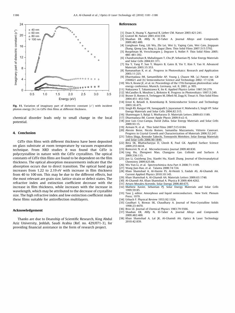
ARTICLE IN PRESS
0.50
4
8
12
16
20
24
Imag
inar
y pa
rt of
die
lect
ric c
onst
ant (
ε'')
Energy (eV)
40 nm60 nm80 nm100 nm
1.0 1.5 2.0 2.5 3.0 3.5
Fig. 11. Variation of imaginary part of dielectric constant (e00) with incident
photon energy (hn) in CdTe thin films at different thickness.
A.A. Al-Ghamdi et al. / Optics & Laser Technology 42 (2010) 1181–11861186
chemical disorder leads only to small change in the localpotential.
4. Conclusion
CdTe thin films with different thickness have been depositedon glass substrate at room temperature by vacuum evaporationtechnique. From XRD studies it was found that CdTe ispolycrystalline in nature with the CdTe crystallites. The opticalconstants of CdTe thin films are found to be dependent on the filmthickness. The optical absorption measurements indicate that theabsorption occurs due to direct transition. The optical band gapincreases from 1.22 to 2.19 eV with increase in film thicknessfrom 40 to 100 nm. This may be due to the different effects, butthe most relevant are grain size, lattice strain or defect states. Therefractive index and extinction coefficient decrease with theincrease in film thickness, while increases with the increase inwavelength, which may be attributed to the decrease of crystallitesize. The high refractive index and low extinction coefficient makethese films suitable for antireflection multilayers.
Acknowledgement
Thanks are due to Deanship of Scientific Research, King AbdulAziz University, Jeddah, Saudi Arabia (Ref. no. 429/071-3), forproviding financial assistance in the form of research project.
References
[1] Duan X, Huang Y, Agarwal R, Lieber CM. Nature 2003;421:241.[2] Gratzel M. Nature 2001;414:338.[3] Shaaban ER, Afify N, El-Taher A. Journal Alloys and Compounds
2009;482:400.[4] Lianghuan Fang, Lili Wu, Zhi Lei, Wei Li, Yaping Cain, Wei Cain, Jingquan
Zhang, Qiong Lou, Bing Li, Jiagui Zhen. Thin Solid Films 2007;515:5792.[5] Burgelman M, Verschraegen J, Degrave S, Nollet P. Thin Solid Films 2005;
480–481:392.[6] Chandramohan R, Mahalingam T, Chu JP, Sebastian PJ. Solar Energy Materials
and Solar Cells 2004;81:371.[7] Xia Y, Yang P, Sun Y, Mayers B, Gates B, Yin Y, Kim F, Yan H. Advanced
Materials 2003;15:353.[8] Ramanathan K, et al. Progress in Photovoltaics: Research and Application
2003;11:225.[9] Dharmadasa IM, Samantilleke AP, Young J, Chaure NB. (a) Patent no: GB
2384621 and (b) Semiconductor Science and Technology 2002; 17:1238.[10] Wu X, Keane JC, et al. in: Proceedings of the 17th European photovoltaic solar
energy conference, Munich, Germany, vol. II, 2001, p. 995.[11] Nakazawa T, Takamizawa K, Ito K. Applied Physics Letter 1987;50:279.[12] McCandles B, Moulton L, Birkmire R. Progress in Photovoltaics 1997;5:249.[13] Btzner D, Romeo A, Terheggen M, Dfbeli M, Zogg H, Tiwari A. Thin Solid Films
2004;451–452:536.[14] Ernst K, Belaidi A, Konenkamp R. Semiconductor Science and Technology
2003;18:475.[15] Singh RS, Rangari VK, Sanagapalli S, Jayaraman V, Mahendra S, Singh VP. Solar
Energy Materials and Solar Cells 2004;82:315.[16] Shanmugan S, Balaji S, Mutharasu D. Materials Letters 2009;63:1189.[17] Dharmadasa IM. Curent Apple Physis 2009;9:e2–6.[18] Jose Luis Cruz-Campa, David Zubia. Solar Energy Materials and Solar Cells
2009;93:15.[19] Armani N, et al. Thin Solid Films 2007;515:6184.[20] Alessio Boise, Nicola Romeo, Samantha Mazzamuto, Vittorio Canevari.
Progress in Crystal Growth and Characterization of Materials 2006;52:247.[21] Tohru Shiga, Kensuke Takechi, Tomoyoshi Motohiro. Solar Energy Materials
and Solar Cells 2006;90:1849.[22] Bera SK, Bhattacharyya D, Ghosh R, Paul GK. Applied Surface Science
2009;255:6634.[23] Romcevic N, et al. Microelectronics Journal 2009;40:830.[24] Ling Hu, Zhengwei Mao, Changyou Gao. Colloids and Surfaces A
2009;336:115.[25] Jun Li, Guizheng Zou, Xiaofei Hu, Xiaoli Zhang. Journal of Electroanalytical
Chemistry 2009;625:88.[26] Wu Yun-Li, et al. Spectrochimica Acta Part A 2008;71:1199.[27] Wang Jian-Hao, et al. Talanta 2008;74:724.[28] Khan Shamshad A, Al-Hazmi FS, Al-Heniti S, Faidah AS, Al-Ghamdi AA.
Current Applied Physics 2010;10:145.[29] Khan Shamshad A, Al-Ghamdi AA. Materials Letters 2009;63:1740.[30] Al-Ghamdi AA, Khan Shamshad A. Physica B 2009;404:4262.[31] Arturo Morales-Acevedo. Solar Energy 2006;80:675.[32] Mathew Xavier, Sebastian PJ. Solar Energy Materials and Solar Cells
1999;59:85.[33] Tauc J, editor. Amorphous and liquid semiconductors. New York: Plenum
Press; 1979.[34] Urbach F. Physical Review 1953;92:1324.[35] Caudhari S, Biswas SK, Chaudhary A. Journal of Non-Crystalline Solids
1998;23:4470.[36] Brus LE. Journal of Chemical Physics 1983;79:5566.[37] Shaaban ER, Afify N, El-Taher A. Journal Alloys and Compounds
2009;482:400.[38] Khan Shamshad A, Lal JK, Al-Ghamdi AA. Optics & Laser Technology
2010;42:839.