CdS Microspheres Composed of Nanocrystals and Their Photocatalytic Activity
Upload
independentCategory
view
3download
0
SHI induced enhancement in green emission from nanocrystallineCdS thin films for photonic applications
Pragati Kumar a,n, Nupur Saxena b,1, Ramesh Chandra c, Kun Gao d, Shengqiang Zhou d,Avinash Agarwal a, Fouran Singh b, Vinay Gupta e, D. Kanjilal b
a Department of Physics, Bareilly College, Shahmat Ganj Road, Bareilly 243005, Uttar Pradesh, Indiab Inter University Accelerator Centre, Aruna Asaf Ali Marg, P.O. Box 10502, New Delhi 110067, Indiac Institute Instrumentation Centre, Indian Institute of Technology, Roorkee 247667, Indiad Institute of Ion Beam Physics and Materials Research, Helmholtz-Zentrum Dresden-Rossendorf (HZDR), P.O. Box 510119, 01314 Dresden, Germanye Department of Physics & Astrophysics, Delhi University, Delhi 110007, India
a r t i c l e i n f o
Article history:Received 21 July 2013Received in revised form30 October 2013Accepted 5 November 2013Available online 13 November 2013
Keywords:Nanocrystalline CdS thin filmsPulsed laser depositionIon beam irradiationPhotoluminescence
a b s t r a c t
Intense green emission is reported from nanocrystalline CdS thin films grown by pulsed laser deposition.The effect of ion beam induced dense electronic excitation on luminescence property of CdS films isexplored under irradiation using 70 MeV 58Ni6þ ions. It is found that swift heavy ion beam irradiationenhances the emission intensity by an order of 1 and broadens the emission range. This feature isextremely useful to enhance the performance of different photonic devices like light emitting diodes andlasers, as well as luminescence based sensors. To examine the role of energy relaxation process of swiftheavy ions in creation/annihilation of different defect levels, multi-peaks are fitted in photoluminescencespectra using a Gaussian function. The variation of contribution of different emissions in green emissionwith ion fluence is studied. Origin of enhancement in green emission is supported by variouscharacterization techniques like UV–visible absorption spectroscopy, glancing angle X-ray diffraction,micro-Raman spectroscopy and transmission electron microscopy. A possible mechanism of enhanced GEdue to ion beam irradiation is proposed on the basis of existing models.
& 2013 Elsevier B.V. All rights reserved.
1. Introduction
Emission in blue and green spectral regions from thin films ofwide bandgap II–VI semiconductors makes them extensivelyinteresting for many applications. In particular, CdS thin filmsattract extra attention as their bandgap emission is expected to liein the proximity of the highest sensitivity of the human eye, i.e.,green light. The thin films of CdS nanoparticles (NPs) have wideapplications in photonic devices like lasers [1,2], light emittingdiodes (LEDs) [3,4], and solar cell [5,6]. Various methods have beenused by different researchers to synthesize CdS nanocrystals thinfilms [1–16]. It has been shown that focused pulsed laser beam onthe target results in rapid temperature rise (41011 K/s) whichmaintains stoichiometry of film and makes pulsed laser deposition(PLD) as a versatile technique [8]. High-energy atoms and ions inthe laser-induced plasma plume create a high surface mobilitywhich accounts for growth of high quality films at a relatively lowsubstrate temperature by PLD [9]. A lot of work has been reported
on PLD grown CdS films investigating the effect of variousparameters such as substrates, substrate temperature, laserfluence, and laser wavelength [1,2,7–14]. Ullrich et al. [14]reported that the challenge for current photonics and optoelec-tronics is to obtain a stable source of green emission (GE) for manydevice applications. Recently our group [17] has reported GE inpulsed laser deposited CdS (PLDCdS) thin films and studied theeffect of thermal annealing on its luminescence property.
Swift heavy ion (SHI) irradiation has evolved as a versatile toolfor materials engineering in the last decade [15,16,18–22]. It is aunique tool among all the different post-deposition techniquesused in practice, because of its capability to deposit very highenergy in localized regions of the material in a controlled manner.Highly energetic ions having velocity comparable to or higher thanthe orbital velocity of the electrons of target lattice atoms; therebythe energy dissipation in the lattice takes place mainly throughelectronic excitation and ionization. A huge amount of energy istransferred rapidly during the electronic excitation within anarrow cylindrical region along the path of the heavy ions, calledion tracks, which results in a variety of controlled modifications inmaterials, including high pressure phase generation [22], defectcreation, defect annealing, crystallization, amorphization, etc.[23,24]. The energy-transfer process in materials during
Contents lists available at ScienceDirect
journal homepage: www.elsevier.com/locate/jlumin
Journal of Luminescence
0022-2313/$ - see front matter & 2013 Elsevier B.V. All rights reserved.http://dx.doi.org/10.1016/j.jlumin.2013.11.026
n Corresponding author. Tel.: þ91 581 2568844; fax: þ91 581 2567808.E-mail address: [email protected] (P. Kumar).1 Present Address: Department of Physics & Astrophysics, University of Delhi,
Delhi 110007, India.
Journal of Luminescence 147 (2014) 184–189

interaction with SHI is explained mainly by Coulomb explosion[25] and thermal spike models [26,27]. The effect of swift heavyion irradiation on various properties of CdS thin films grown bydifferent deposition techniques [15,16,18–21] has been reported.To the best of our knowledge, electronic excitation inducedenhancement of luminescence in PLDCdS thin films is not yetreported.
In the present article, we have explored the effect of electronicexcitation by means of SHI on luminescence properties of PLDCdSthin films. Here, we demonstrate stable, intense, and broad GE as aconsequence of SHI irradiation on PLDCdS thin films. Theenhanced luminescence seeks wide applications in fluorescentsensors, green LEDs and other existing photo-electronic devices.
2. Experimental
Thin films of CdS NPs are deposited by laser ablation of a targetprepared by pressing and sintering the chemically synthesized CdSquantum dots (QDs). The synthesis of CdS QDs in powder form isreported elsewhere [28]. For PLD, an ultraviolet laser source: apulsed excimer KrF laser operating at 248-nm wavelength (pulsewidth of 10 ns and repetition rate 10 Hz), has been used. The laserbeam of energy 300 mJ/pulse is focused onto a rotating targetmounted at an oblique angle of 301 with respect to the incidentlaser beam. The distance between target and substrate is kept as5.5 cm. The films are deposited on single-crystal (111) n-typesilicon wafers, glass and carbon-coated Cu grids (for TEM) sub-strates at a temperature of 200 1C inside a clean stainless steel(SS304) vacuum chamber with a base pressure of 5�10�6 Torr.The CdS films of thickness �250 nm were deposited at rate�0.025 nm/pulse. To study the ion irradiation effect on structuraland optical properties, thin films so prepared are irradiated with70 MeV Ni6þ ions using the 15 UD Pelletron Accelerator at InterUniversity Accelerator Centre (IUAC), New Delhi, India. The SHIirradiation is carried out in an experimental chamber having avacuum of 2�10�6 Torr at room temperature keeping ion beamcurrent as �1 pnA (particle nano-Ampere). The beam is scannedover an area of �1 cm2 of the sample with an electromagneticscanner to ensure the uniformity of irradiation. The stopping andrange of ions in matter (SRIM) simulations [29] indicate theelectronic energy loss, nuclear energy loss, and range of theincident 70 MeV Ni ion in CdS as 10.58 keV/nm, 0.031 keV/nmand 10.94 mm respectively. Therefore, the ions get buried in thesubstrate only and not in the film. The irradiation dose or ionfluence is varied from 1�1012 to 1�1014 ions/cm2 for the study.
Glancing angle X-ray diffraction (GAXRD) studies are carriedout at a glancing angle of 11 using a Bruker D8 diffractometer
(Cu Kα radiation, λ¼1.54 Å) and micro-Raman spectroscopy usinga Renishaw Invia Raman microscope with excitation wavelength of514 nm from an Ar-ion laser. The samples are examined bytransmission electron microscopy (TEM) using a Tecnai G20-Stwin operating at 200 kV with point resolution of 1.44 Å, lineresolution of 2.32 Å, and line-type super-twin lenses. The filmsdeposited on glass substrates are analyzed using UV–vis absorp-tion spectroscopy (Hitachi 3300 UV/visible spectrophotometer).Photoluminescence (PL) studies are carried out at room tempera-ture using a Jobin Yvon Triax 550 monochromator combined witha liquid-nitrogen cooled InGaAs detector. A He–Cd laser (wave-length 325 nm) is used as the excitation source.
3. Results and discussion:
The glancing angle X-ray diffraction (GAXRD) patterns of the asgrown CdS thin film irradiated at different fluences are shown inFig. 1. It is clear from the diffraction patterns that as-grown CdSfilms exhibit a preferred orientation corresponding to (1 1 1) planeof cubic (zinc blende) phase at an angle 2θ�26.641 with otherdiffraction peaks at 36.81 and 48.11 corresponding to (1 0 2) and(1 0 3) planes of the hexagonal structure, respectively. Theobserved significant reduction in peak intensity of plane (1 1 1)and small increase in FWHM for films irradiated with fluences of1�1012 and 1�1013 ions/cm2 show reduction in crystallinity andparticle size, respectively. It has been reported by various groupsthat it might be due to the formation of point defects, defectclusters, or creation of additional grain boundaries [21,30,31] dueto SHI irradiation. In addition, we observed very small compressivestress for the as-deposited film as evident from the shift of (1 1 1)peak by 0.11 towards higher diffraction angles from its correspond-ing value for bulk (2θ¼26.551; JCPDS 750581). It may be due toresidual stress produced in the film during deposition or due tothe lattice mismatch between the film and substrate [15]. Thiscompressive stress is enhanced in films after SHI irradiation andthe peak position gets shifted towards higher diffraction angles i.e.2θ¼26.681 and 26.731 for films irradiated at a fluence of 1�1012
and 1�1013 ions/cm2 respectively. Besides, emergence of a newpeak at angle 2θ�43.771 corresponding to plane (1 1 0) is noticedfor films irradiated with same fluences. Chandramohan et al. [15]reported that the shift in peak position is attributed to themodification of lattice strain and development of new peak maybe due to specific preferential orientation during recrystallizationinduced by SHI. Since the dense electronic excitation induced bySHI can result in a transient growth of the lattice temperature tovery high values leading to large amplitude oscillations in thelattice, bond-breaking phenomena associated with atomic displa-cements followed by certain collective atomic rearrangementsoccur [32]. On further increasing the fluence, peak intensity isincreased considerably with a small shift in peak position towardslower diffraction angle. The increase in peak intensity indicatesimprovement in crystallinity and grain size. It has been reportedby different groups that this may be due to defect annealing[21,30,31]. Besides, structural phase transition from mixed phaseto cubic phase is observed in the sample irradiated at a fluence of1�1014 ions/cm2 as indicated by disappearance of planes (1 1 0)and (1 0 3). Such a structural phase transition has been recentlyreported by our group [17] in PLDCdS films and by Benyagoub inZrO2 and HfO2 [33]. The phase transition may be attributed toatomic rearrangements caused by SHI induced dense electronicexcitations.
In the present study, we observed five optical vibrationalRaman active modes at �302.4 cm�1, 391 cm�1, 603 cm�1,690 cm�1 and 904 cm�1 in all samples as shown in Fig. 2. Theintense and broad peaks at �302 cm�1, 603 cm�1 and 904 cm�1
Fig. 1. GAXRD pattern of CdS thin films irradiated at different fluences.
P. Kumar et al. / Journal of Luminescence 147 (2014) 184–189 185

are assigned to the fundamental optical phonon mode (LO), thefirst overtone mode (2LO) and the second overtone mode (3LO) ofCdS respectively. These are in agreement with previous reports[17,34]. The shifting of LO peak towards lower frequency side fromthat of its corresponding value for bulk CdS (�305 cm�1) indi-cates phonon confinement due to reduction in particle size [34].Ion beam causes an increase in intensity with shifting of�0.5 cm�1, 2 cm�1 and 1 cm�1 in the 1LO peak towards lowerwavenumber (inset in Fig. 2), from that of the correspondingpristine film, for the films exposed to fluence 1�1012, 1�1013
and 1�1014 ions/cm2 respectively. The shifting of peak may beattributed to phonon localization by high density of lattice defects[35] and/or structural strain induced grain fragmentation due toenergetic heavy ions. The weak Raman peaks at �390 cm�1 and690 cm�1 result from multiphonon scattering. They have been
identified and confirmed by low frequency Raman measurementrecently by our group [17] as those corresponding to the vibra-tional modes 1LOþ2E2 and 2LOþ2E2 respectively.
The average particle size is calculated from TEM micrographs.TEM micrographs of pristine and 1�1013 ions/cm2 irradiated CdSthin films are shown in Fig. 3a and c respectively. Fig. 3b and dshows the lognormal fitting in corresponding size distributions. Itis found that the standard deviation is enhanced from 0.12 to 0.27with reduction in average size from �9.2 nm to 4.8 nm (around48%) for pristine CdS film compared to film irradiated at a fluenceof 1�1013 ions/cm2.
UV–visible absorption studies are carried out to study the effectof ion irradiation fluence on the bandgap of CdS thin films. Theinset in Fig. 4 shows Tauc's plots of pristine and irradiated filmswith different fluences. The direct bandgap values are estimated as�2.46 eV, 2.55 eV, 2.62 eV, and 2.56 eV for the as-depositedsample and the sample irradiated with fluences of 1�1012,1�1013 and 1�1014 ions/cm2 respectively. It is obvious that thebandgap of pristine film is blue-shifted with respect to thebandgap of bulk CdS (�2.42 eV) due to quantum confinement.The average radius of particle is calculated using the massapproximation formula for energy shift given by Wang and Herron[36] as follows:
ΔE¼ ℏ2π2
2R2
1me
þ 1mn
� ��1:789e2
εR�02:48En
RY ð1Þ
where R is radius of particle, me¼0.19mo and mh¼0.80mo areeffective masses of electron and hole for CdS respectively, ε¼5.7 isthe dielectric constant of CdS and En
RY is effective Rydberg energy.The average sizes for pristine sample and the samples irradiatedwith 1�1012, 1�1013 and 1�1014 ions/cm2
fluences are found tobe 12.8 nm, 8.7 nm, 7 nm and 8.4 nm respectively. It can bededuced from this that the particle size is reduced by 45% for
Fig. 2. Raman spectra of CdS thin films irradiated at different fluences. Inset:normalized intensity vs Raman shift of 1LO mode.
Fig. 3. TEM micrograph of thin film of CdS nanocrystals: (a) pristine, (b) particle size distribution of pristine, (c) irradiated at 1�1013 ions/cm2 and (d) its particle sizedistribution. Solid curve represents lognormal distribution in (b) and (d).
P. Kumar et al. / Journal of Luminescence 147 (2014) 184–189186
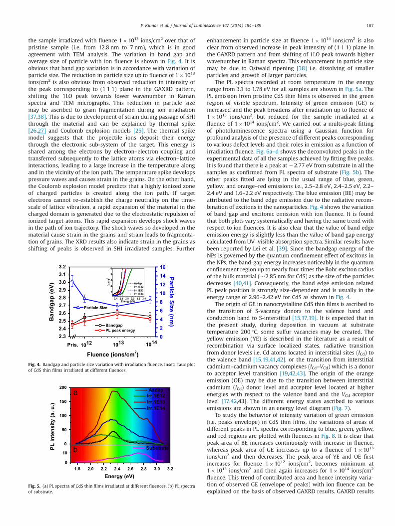
the sample irradiated with fluence 1�1013 ions/cm2 over that ofpristine sample (i.e. from 12.8 nm to 7 nm), which is in goodagreement with TEM analysis. The variation in band gap andaverage size of particle with ion fluence is shown in Fig. 4. It isobvious that band gap variation is in accordance with variation ofparticle size. The reduction in particle size up to fluence of 1�1013
ions/cm2 is also obvious from observed reduction in intensity ofthe peak corresponding to (1 1 1) plane in the GAXRD pattern,shifting the 1LO peak towards lower wavenumber in Ramanspectra and TEM micrographs. This reduction in particle sizemay be ascribed to grain fragmentation during ion irradiation[37,38]. This is due to development of strain during passage of SHIthrough the material and can be explained by thermal spike[26,27] and Coulomb explosion models [25]. The thermal spikemodel suggests that the projectile ions deposit their energythrough the electronic sub-system of the target. This energy isshared among the electrons by electron–electron coupling andtransferred subsequently to the lattice atoms via electron–latticeinteractions, leading to a large increase in the temperature alongand in the vicinity of the ion path. The temperature spike developspressure waves and causes strain in the grains. On the other hand,the Coulomb explosion model predicts that a highly ionized zoneof charged particles is created along the ion path. If targetelectrons cannot re-establish the charge neutrality on the time-scale of lattice vibration, a rapid expansion of the material in thecharged domain is generated due to the electrostatic repulsion ofionized target atoms. This rapid expansion develops shock wavesin the path of ion trajectory. The shock waves so developed in thematerial cause strain in the grains and strain leads to fragmenta-tion of grains. The XRD results also indicate strain in the grains asshifting of peaks is observed in SHI irradiated samples. Further
enhancement in particle size at fluence 1�1014 ions/cm2 is alsoclear from observed increase in peak intensity of (1 1 1) plane inthe GAXRD pattern and from shifting of 1LO peak towards higherwavenumber in Raman spectra. This enhancement in particle sizemay be due to Ostwald ripening [38] i.e. dissolving of smallerparticles and growth of larger particles.
The PL spectra recorded at room temperature in the energyrange from 3.1 to 1.78 eV for all samples are shown in Fig. 5a. ThePL emission from pristine CdS thin films is observed in the greenregion of visible spectrum. Intensity of green emission (GE) isincreased and the peak broadens after irradiation up to fluence of1�1013 ions/cm2, but reduced for the sample irradiated at afluence of 1�1014 ions/cm2. We carried out a multi-peak fittingof photoluminescence spectra using a Gaussian function forprofound analysis of the presence of different peaks correspondingto various defect levels and their roles in emission as a function ofirradiation fluence. Fig. 6a–d shows the deconvoluted peaks in theexperimental data of all the samples achieved by fitting five peaks.It is found that there is a peak at �2.77 eV from substrate in all thesamples as confirmed from PL spectra of substrate (Fig. 5b). Theother peaks fitted are lying in the usual range of blue, green,yellow, and orange–red emissions i.e., 2.5–2.8 eV, 2.4–2.5 eV, 2.2–2.4 eV and 1.6–2.2 eV respectively. The blue emission (BE) may beattributed to the band edge emission due to the radiative recom-bination of excitons in the nanoparticles. Fig. 4 shows the variationof band gap and excitonic emission with ion fluence. It is foundthat both plots vary systematically and having the same trend withrespect to ion fluences. It is also clear that the value of band edgeemission energy is slightly less than the value of band gap energycalculated from UV–visible absorption spectra. Similar results havebeen reported by Lei et al. [39]. Since the bandgap energy of theNPs is governed by the quantum confinement effect of excitons inthe NPs, the band-gap energy increases noticeably in the quantumconfinement region up to nearly four times the Bohr exciton radiusof the bulk material (�2.85 nm for CdS) as the size of the particlesdecreases [40,41]. Consequently, the band edge emission relatedPL peak position is strongly size-dependent and is usually in theenergy range of 2.96–2.42 eV for CdS as shown in Fig. 4.
The origin of GE in nanocrystalline CdS thin films is ascribed tothe transition of S-vacancy donors to the valence band andconduction band to S-interstitial [15,17,19]. It is expected that inthe present study, during deposition in vacuum at substratetemperature 200 1C, some sulfur vacancies may be created. Theyellow emission (YE) is described in the literature as a result ofrecombination via surface localized states, radiative transitionfrom donor levels i.e. Cd atoms located in interstitial sites (ICd) tothe valence band [15,19,41,42], or the transition from interstitialcadmium–cadmium vacancy complexes (ICd–VCd) which is a donorto acceptor level transition [19,42,43]. The origin of the orangeemission (OE) may be due to the transition between interstitialcadmium (ICd) donor level and acceptor level located at higherenergies with respect to the valence band and the VCd acceptorlevel [17,42,43]. The different energy states ascribed to variousemissions are shown in an energy level diagram (Fig. 7).
To study the behavior of intensity variation of green emission(i.e. peaks envelope) in CdS thin films, the variations of areas ofdifferent peaks in PL spectra corresponding to blue, green, yellow,and red regions are plotted with fluences in Fig. 8. It is clear thatpeak area of BE increases continuously with increase in fluence,whereas peak area of GE increases up to a fluence of 1�1013
ions/cm2 and then decreases. The peak area of YE and OE firstincreases for fluence 1�1012 ions/cm2, becomes minimum at1�1013 ions/cm2 and then again increases for 1�1014 ions/cm2
fluence. This trend of contributed area and hence intensity varia-tion of observed GE (envelope of peaks) with ion fluence can beexplained on the basis of observed GAXRD results. GAXRD results
Fig. 4. Bandgap and particle size variation with irradiation fluence. Inset: Tauc plotof CdS thin films irradiated at different fluences.
Fig. 5. (a) PL spectra of CdS thin films irradiated at different fluences. (b) PL spectraof substrate.
P. Kumar et al. / Journal of Luminescence 147 (2014) 184–189 187

clearly show that the evolution of planes (1 1 0) takes place at thecost of evaporation of planes (1 0 2) and reduction of planes (1 0 3)at fluence of 1�1012 ions/cm2. We assumed that drasticallyenhanced contribution of YE and OE emissions is due to thecreation of additional ICd–VCd and ICd energy states during recrys-tallization due to electronically activated movement of Cd atomsfrom one minimum to the next lower minimum by crossing a
potential barrier. Kulp and Kelley [44] and Lozada-Morales andZelaya-Angel [42] reported that the displacement of Cd atom to aninterstitial position is easier than that of the S atom under highenergy electron bombardment, indicating that Cd atoms have asmaller energy bound than do S atoms in the CdS lattice. More-over, thermal oscillation amplitude experienced by Cd atoms islarger than that of S atoms in crystalline CdS, as reported by Bocchiand Ghezzi [45] such that the mean-square displacement of agiven atom is inversely proportional to the force constant whichdescribes the interaction between similar atoms i.e. Cd–Cd or S–Sin the lattice. They observed experimentally that the interactionbetween S–S atoms is stronger than the interaction betweenCd–Cd atoms. Given these arguments, it is expected that SHIinduced electronic excitation would produce a higher ICd, ICd–VCd
than Is–Vs and defect population that rationalizes the observedenhance area of YE and GE with a justification of approximatedouble enhancement in area of YE than that of GE (Fig. 8). It isfascinating that area contributed by YE is highly suppressed to thatof GE for the sample irradiated with fluence of 1�1013 ions/cm2
and the envelope of emission peaks shifts towards higher energy.This is ascribed to increased population density of Is–Vs andreduction in ICd or ICd–VCd, which may be due to reduction in the(1 0 3) diffraction plane and enhancement of (1 1 0) plane duringrecrystallization. Though here no phase transition is observed upto fluence 1�1013 ions/cm2 disappearance of plane (102) andevolution of plane (110) indicate that SHI induced displacement ofatoms from one minimum of energy state to the other minimatakes place. Initially at lower fluence of 1�1012 ions/cm2 Cd atomswere displaced more rapidly than S atoms but at relatively higherfluence (1�1013 ions/cm2) displacement of S atom is drasticallyincreased and hence the contribution of GE emission, which isrelated to the transition of S-vacancy donors to the valence bandand conduction band to S-interstitial. Further increase in fluenceresults in increase of area contributed by YE and OE with drop inGE contribution, which results in reduction of emission strength. Itmay be due to reduction in population density of S vacancieswhich may be related to the disappearance of diffraction peakscorresponding to (1 1 0) and (1 0 3) planes. It is expected that atfluence 1�1014 ions/cm2, the particle size is further reduced,causing the dissolution of smaller crystals, and the growth of
Fig. 6. Gaussian fittings of PL spectrum for different samples. Circles represent the experimental data, while the solid curves indicate peak sum of fittings to the experimentaldata. The five peaks are shown by different symbols corresponding to different emissions: (star) substrate, (square) BE, (upper triangle) YE, (lower triangle) GE, (diamond)OE.
Fig. 7. Schematic diagram of different energy levels in CdS thin films.
Fig. 8. Variation in contributed area of different colors in the PL of all samples.(For interpretation of the references to color in this figure legend, the reader isreferred to the web version of this article.)
P. Kumar et al. / Journal of Luminescence 147 (2014) 184–189188

larger particles may be due to Ostwald ripening [38]. It isconfirmed by observed red-shift of blue emission peak in PLspectra, shifting of 1LO Raman peaks towards higher wavenumber,reduction of bandgap and increase in diffraction peak intensity.The grain growth results in reduction of surface to volume ratioand hence population density of defect levels which leads to adrop in quantum efficiency.
4. Conclusion
To conclude, the effect of SHI induced dense electronic excita-tion on PLD grown thin films of nanocrystalline CdS has beeninvestigated. It is observed that the GE from the as-deposited CdSthin film becomes intense and broad after swift heavy ionsirradiation. The observed broad GE from irradiated samples coversalmost full range of visible spectrum. The broadness of thespectrum is ascribed to the enhanced size distribution, creationof defect levels and grain fragmentation. SHI induced grainfragmentation is the possible mechanism for observed reductionin particle size and enhanced band gap at a fluence of 1�1013
ions/cm2 in the present study. The reduction in bandgap at fluenceof 1�1014 ions/cm2 is attributed to ion beam induced graingrowth due to Ostwald ripening.
Acknowledgments
The authors are thankful to Dr. R. P. Singh, Principal, BareillyCollege, Bareilly, for providing necessary facilities and moralsupport. One of the authors (NS) is thankful to University GrantCommission (UGC), India, for providing Dr. D.S. Kothari PostDoctoral Fellowship. The assistance provided by Mr. Ravish Jainand Mr. Paritosh Dubey, Indian Institute of Technology, Roorkee,during thin film deposition is highly appreciated. The team workdone by the Pelletron Group, IUAC, New Delhi, during irradiationexperiment is highly appreciable. The help received fromMr. Pawan Kulariya and Dr. Vinod Kumar, IUAC, New Delhi, inGAXRD measurements and Raman measurements is gratefullyacknowledged. The work at HZDR is supported by theHelmholtz-Gemeinschaft Deutscher Forschungszentren (HGF-VH-NG-713).
References
[1] B. Ullrich, D.M. Bagnall, H. Sakai, Y. Segawa, J.X. Hai, J.L. Xin, J. Lumin. 87–89(2000) 1162.
[2] D.M. Bagnall, B. Ullrich, H. Sakai, Y. Segawa, J. Cryst. Growth 214–215 (2000)1015.
[3] M.V. Artemyev, V. Sperling, U. Woggon, J. Appl. Phys. 81 (1997) 6975.[4] J. Nanda, K.S. Narayan, B.A. Kuruvilla, G.L. Murthy, D.D. Sarma, Appl. Phys. Lett.
72 (1998) 1335.
[5] Y.J Shen, Y.L. Lee, Nanotechnology 19 (2008) 045602.[6] S.C. Lin, Y.L. Lee, C.H. Chang, Y.J. Shen, Y.M. Yang, Appl. Phys. Lett. 90 (2007)
143517.[7] I. Martil, G.G. Diaz, F.S. Quesada, M. Rodriguez, Thin Solid Films 90 (1982) 253.[8] W.P. Shen, H.S. Kwok, Appl. Phys. Lett. 65 (1994) 2162.[9] J.A. Greer, J. Vac. Sci. Technol. A 10 (1992) 1821.[10] O. Trujillo, R. Moss, K.D. Vuong, D.H. Lee, R. Noble, D. Finnigan, S. Orloff,
E. Tenpas, C. Park, J. Fagan, X.W. Wang, Thin Solid Films 290-291 (1996) 13.[11] B. Ullrich, H. Sakai, N.M. Dushkina, H. Ezumi, S. Keitoku, T. Kobayashi,
Microelectron. Eng. 43–44 (1998) 695.[12] S.M. Mahdavi, A.I. zad, R.M. Tilaki, Opt. Mater. 27 (2005) 1583.[13] B. Ullrich, H. Sakai, Y. Segawa, Thin Solid Films 385 (2001) 220.[14] B. Ullrich, R. Schroeder, H. Sakai, A. Zhang, S.Z.D. Cheng, Appl. Phys. Lett.
80 (2002) 356.[15] S. Chandramohan, R. Sathyamoorthy, P. Sudhagar, D. Kanjilal, D. Kabiraj,
K. Asokan, V. Ganesan, V. Shripathi, U.P. Deshpande, Appl. Phys. A: Mater.Sci. Process. 94 (2009) 703.
[16] R.R. Ahire, A.A. Sagade, N.G. Deshpande, S.D. Chavhan, R. Sharma, F. Singh,J. Phys. D: Appl. Phys. 40 (2007) 4850.
[17] P. Kumar, N. Saxena, R. Chandra, V. Gupta, A. Agarwal, D. Kanjilal, NanoscaleRes. Lett. 7 (2012) 584.
[18] S. Soundeswaran, O. Senthilkumar, P. Ramasamy, D. Kabiraj, D.K. Avasthi,R. Dhanasekaran, Physica B 355 (2005) 222.
[19] R. Sathyamoorthy, S. Chandramohan, P. Sudhagar, D. Kanjilal, D. Kabiraj,K. Asokan, Sol. Energy Mater. Sol. Cells 90 (2006) 2297.
[20] S. Chandramohan, R. Sathyamoorthy, P. Sudhagar, D. Kanjilal, D. Kabiraj,K. Asokan, Nucl. Instrum. Methods B 254 (2007) 236.
[21] V.V. Ison, A.R. Rao, V. Dutta, P.K. Kulriya, D.K. Avasthi, S.K. Tripathi, J. Appl.Phys. 106 (2009) 023508.
[22] N. Saxena, P. Kumar, A. Agarwal, D. Kanjilal, Phys. Status Solidi A 209 (2012)283.
[23] A. Kamarou, W. Wesch, E. Wendler, Phys. Rev. B 78 (2008) 054111.[24] W. Wesch, A. Kamarou, E. Wendler, Nucl. Instrum. Methods B 225 (2004) 111.[25] R.L. Fleischer, P.B. Price, R.M. Walker, E.L. Hubbard, Phys. Rev. 156 (1967) 353.[26] M. Toulemonde, C. Dufour, E. Paumier, Phys. Rev. B 46 (1992) 14362.[27] G. Szenes, Z.E. Horvath, B. Pecz, F. Paszti, L. Toth, Phys. Rev. B 65 (2002)
045206.[28] P. Kumar, N. Saxena, F. Singh, A. Agarwal, Physica B 407 (2012) 3347.[29] ⟨www.srim.org⟩, 2008.[30] D.C. Agarwal, A. Kumar, S.A. Khan, D. Kabiraj, F. Singh, A. Tripathi, J.C. Pivin,
R.S. Chauhan, D.K. Avasthi, Nucl. Instrum. Methods B 244 (2006) 136.[31] Y.S. Chaudhary, S.A. Khan, R. Shrivastav, V.R. Satsangi, S. Prakash, D.K. Avasthi,
S. Dass, Nucl. Instrum. Methods B 225 (2004) 291.[32] B. Balamurugan, B.R. Mehta, D.K. Avasthi, F. Singh, A.K. Arora, M. Rajalakshmi,
G. Raghavan, A.K. Tyagi, S.M. Sivaprasad, J. Appl. Phys. 92 (2002) 3304.[33] A. Benyagoub, Phys. Rev. B 72 (2005) 094114.[34] D.S. Chuu, C.M. Dai, C.F. Hsieh, C.T. Tsai, J. Appl. Phys. 69 (1991) 8402.[35] F. Singh, R.G. Singh, V. Kumar, S.A. Khan, J.C. Pivin, J. Appl. Phys. 110 (2011)
083520.[36] W. Wang, N. Herron, Phys. Rev. B 42 (1990) 7253.[37] M. Kumar, F. Singh, S.A. Khan, V. Baranwal, S. Kumar, D.C. Agarwal,
A.M. Siddiqui, A. Tripathi, A. Gupta, D.K. Avasthi, A.C. Pandey, J. Phys. D: Appl.Phys. 38 (2005) 637.
[38] D. Mohanta, F. Singh, D.K. Avasthi, A. Choudhury, Cent. Eur. J. Phys. 4 (2006)187.
[39] Y. Lei, W.K. Chim, H.P. Sun, G. Wilde, Appl. Phys. Lett. 86 (2005) 103106.[40] T. Orii, S. Kaito, K. Matsuishi, S. Onari, T. Arai, J. Phys.: Condens. Matter
14 (2002) 9743.[41] M. Agata, H. Kurase, S. Hayashi, K. Yamamoto, Solid State Commun. 76 (1990)
1061.[42] R. Lozada-Morales, O. Zelaya-Angel, Thin Solid Films 281–282 (1996) 386.[43] O. Vigil, I. Riech, M. Garcia-Rocha, O. Zelaya-Angel, J. Vac. Sci. Technol. A
15 (1997) 2282.[44] B.A. Kulp, R.H. Kelley, J. Appl. Phys. 31 (1960) 1057.[45] C. Bocchi, C. Ghezzi, J. Phys. Chem. Solids 36 (1975) 421.
P. Kumar et al. / Journal of Luminescence 147 (2014) 184–189 189
Copyright © 2022 FDOKUMEN