Application of a CdS nanostructured layer in inverted solar cells
Upload
khangminh22Category
view
1download
0
Simulation of the Efficiency of CdS/CdTe Tandem
Multi-Junction Solar Cells
Ashrafalsadat S. Mirkamali1,2
, Khikmat Kh. Muminov1
1S.U.Umarov Physical-Technical Institute, Academy of Sciences of the
Republic of Tajikistan, 299/1 Aini Ave, Dushanbe 734062, Tajikistan
e-mail: [email protected] 2Permanent address: Department of Science and Engineering, Behshahr
Branch, Islamic Azad University, Behshahr, Iran
e-mail: [email protected]
Abstarct
In this paper we study CdS/CdTe solar cells by means of AMPS-1D
software. First we study the effect of thickness of semiconductor layers on the
output parameters of the CdS/CdTe solar cell, such as density of short-circuit
current, open circuit voltage, fill factor and efficiency. Numerical simulation
shows that the highest efficiency of single-junction CdS/CdTe solar cell equal
to 18.3% is achieved when the CdTe layer thickness is 1000 nm and a CdS
layer is 60 nm. Then, in order to obtain the maximal value of the efficiency,
new tandem multi-junction structure consisting of layers of two solar cells
connected with each other back to back are designed and engineered taking into
account the results obtained for the single-junction solar cells. Numerical
simulations show that its highest efficiency in 31.8% can be obtained when the
thickness of CdS p-layer is equal to 50 nm, and the thickness of the CdS n-layer
is equal to 200 nm, while thicknesses of the CdTe n-layer and CdTe p-layer are
kept fixed and equal to 3000 nm and 1000 nm, respectively.

2
INTRODUCTION
It is well known theoretically, that for the cadmium telluride CdTe solar
cells, the minimal thickness of the CdTe film, required to absorb 99% of incident
photons with energies greater than the band gap Eg, is about 1-2 microns [1, 2].
Reducing the thickness of the CdTe absorber layer is reasonable not only in terms
of cost reduction of material in the manufacturing process, but also can improve
the efficiency of the solar cell due to reduction of recombination losses by volume
[3, 4].
However, although the thin films are more compact and free of micropores,
the growth control and even repeated crystallization should be provided for their
preparation [4]. So, in 1982, Tyan et al published an interesting paper on the
CdTe/CdS thin-film solar cells having the efficiency of about 10% [5].
Subsequently, the efficiency of 15.8% was achieved by Ferekides et al. [6].
Finally, a group of the US researchers in the National Renewable Energy
Laboratory have reported a record efficiency of 16.5% [7]. This record-breaking
solar CdS/CdTe cell with the efficiency of 16.5% used a modified structure of the
CTO/ZTO/CdS/CdTe with the CdS layer with the thickness of 0.1 microns and the
CdTe layer of 10 microns. It was produced using three different techniques: close
space sublimation (CSS) for deposition of CdTe film, the method of chemical bath
deposition (CBD) to form a CdS film and magnetron sputtering for the remaining
layers. The resulting record efficiency solar cells (16.5%) is slightly more than half
of the theoretical limit of 29%, but it is believed that practical CdTe devices with
an efficiency of 18-19% can be achieved in the near future [8]. To reduce the
absorption and to minimize the surface recombination current in the CdS/CdTe
solar cells, a reduction of CdS layer thickness has been consistently carried out to
1000 Å and less [9]. At this thickness, they have a low performance due to
increasing the likelihood of shunting.

3
Malaysian group [10] in 2011 has developed a ZnxCd1-xS/CdTe solar cell.
In order to study the effect of thin-film CdTe absorber a numerical simulation by
use AMPS-1D software has been carried out. The thickness of the CdTe absorber
layer varied in the range from 100 nm to 6000 nm at this simulation. Further
reduction in the thickness of CdTe layer from 1 micron showed that the short
circuit current density decreases slowly and the open circuit voltage remains
practically unchanged, while the fill factor increases until a 600 nm [10]. Results
showed that the efficiency of 19.5% could be achieved by use of economical
ultrathin ZnxCd1-xS/CdTe solar cell structures, where the CdTe layer has the
thickness of 1 micron, and the thickness of ZnxCd1-xS is 60 nm, with the ZnO or
Zn2SO4 buffer layers of 100 nm thickness. This solar cell has been studied in terms
of stability to variation of temperature and also other properties of used materials
have been investigated in the paper [11].
The purpose of this study is numerical simulation of CdS/CdTe in hetero-
junction and multi-junction tandem solar cells and determining the optimal
structure of the last, which would have a highest efficiency of conversion.
THIN FILM CdS/CdTe SOLAR CELLS
Thin film solar cells require less semiconductor material and it is easier to
manufacture and assemble, they has less weight, they are flexible and less
expensive than wafer solar cells. To date, there are a number of thin-film materials
such as cadmium telluride CdTe, copper indium diselenide CIS, which are
developed as materials for hetero-junction solar cells. Materials for production of
thin-film heterojunction solar cells include such materials as gallium arsenide
GaAs, indium phosphide InP, amorphous silicon a-Si, polycrystalline silicon, and
so on. Such a material like CdTe is well deposited and well suited for large-scale

4
production, however, cadmium is toxic. Small variations of CIS, obtainable by
adding gallium gives a copper indium/gallium diselenide (CIGS), which shows the
highest efficiency.
Cadmium telluride (CdTe) is a typical p-type semiconductor of II-VI group
having an optical band gap of 1.5 eV, which is optimal one for photogeneration.
The ability to uniform sputtering and a wide range of thermodynamic stability
implies that the conventional sputtering process can be easily used for the
deposition of the CdTe film on substrates with a large area [12].
Typical structure of the CdTe/CdTe solar cell is shown in Fig. 1. Its
manufacturing usually begins on a glass substrate on which a thin layer of In2O3-
SnO2 (ITO) as a transparent conductive oxide (TCO) is deposited. The thickness of
this layer is chosen such as to ensure both the conductivity and the optical
transparency. As a window lyer there Cd n-type layer serve [12]. Then, on the
layer enriched by tellurium various metals (Zn [13] Sb [14], Au [15], usually
copper or Cu [15, 16]) are deposited with the graphite paste, so as to form a contact
metal/metal telluride.
Figure 1. Typical structure of the CdTe/CdTe solar cell [13]
LIGH
T
front back
X=0
Position (X, μm)
ITO
(2
00
nm
)
Cd
S (
20
0n
m)
Cd
Te
(2
-5 μ
nm
)
Cu
(g
rafi
te p
ast
e)
9

5
Numerical simulation of the solar cells is an important step in the analysis
of their structure and properties, especially, in order to determine the influence of
variations in the structure and properties of their individual parts on the efficiency
of the solar cell as a whole. In general, such an analysis can be done by owning,
sufficiently information about the characteristics of the input data. Optoelectronic
properties of the materials from which the layers are produced, used in the
numerical modeling, were taken from the paper of Gloeckler [18] devoted to thin-
film photovoltaic cells. Profile of absorption (absorbance) was calculated by the
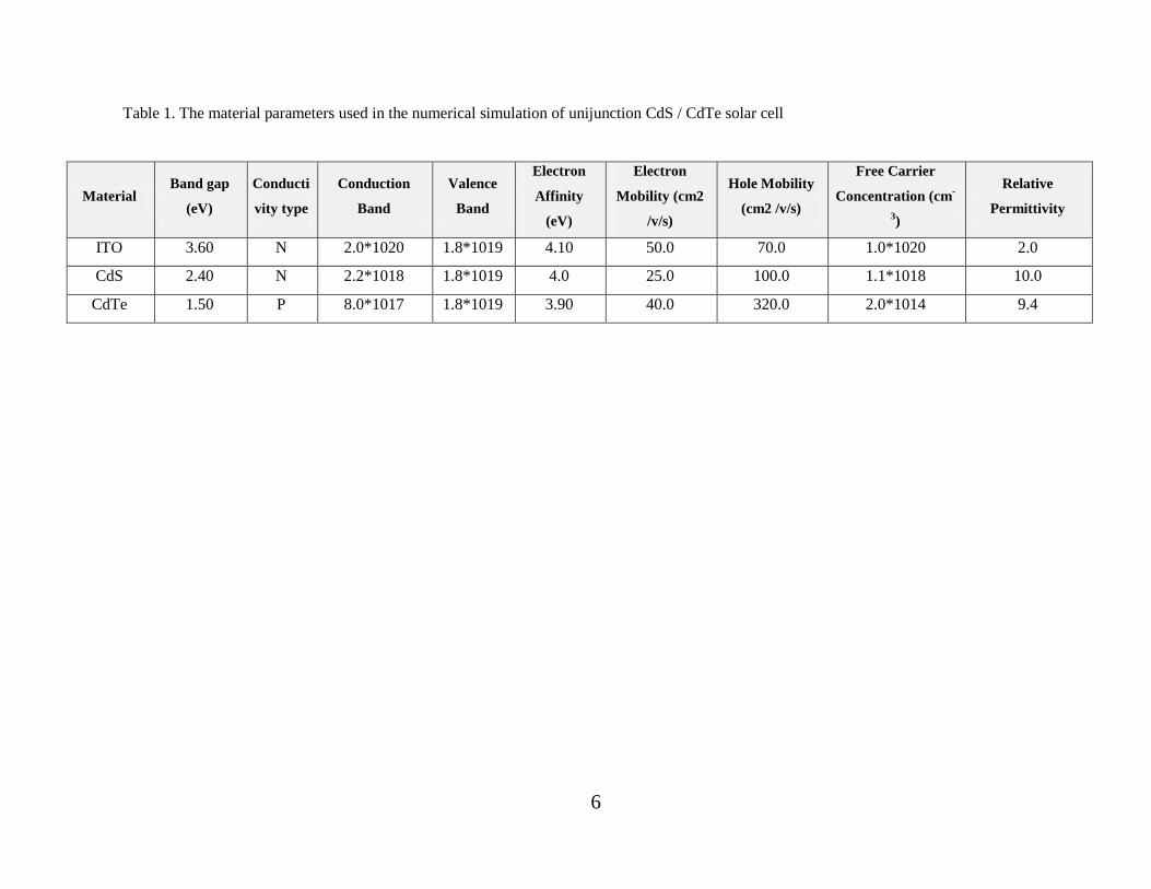
Brownson et al. [19]. The values of materials parameters used in this simulation
are shown in Table 1. In this study, as the material from which the front absorbent
layer is made, i.e. the absorber material, is CdS with the bandgap (2.4 eV) to
absorb ultra-violet region of the standard AM 1.5 solar spectrum. A layer of p-type
in this study is the CdTe (1.5 eV). Transparent thin layer of indium oxide In2O3-
SnO2 with a bandgap of 3.60 eV (ITO) is used as the transparent conductive
contacts, i.e. a material that covers the front surface of the oxide layer.
6
Table 1. The material parameters used in the numerical simulation of unijunction CdS / CdTe solar cell
Material Band gap
(eV)
Conducti
vity type
Conduction
Band
Valence
Band
Electron
Affinity
(eV)
Electron
Mobility (cm2
/v/s)
Hole Mobility
(cm2 /v/s)
Free Carrier
Concentration (cm-
3)
Relative
Permittivity
ITO 3.60 N 2.0*1020 1.8*1019 4.10 50.0 70.0 1.0*1020 2.0
CdS 2.40 N 2.2*1018 1.8*1019 4.0 25.0 100.0 1.1*1018 10.0
CdTe 1.50 P 8.0*1017 1.8*1019 3.90 40.0 320.0 2.0*1014 9.4

7
Theoretically, the minimum thickness of the film CdTe, required to absorb
99% of incident photons with energies greater than the band gap is approximately
1-2 mm [20, 21]. In this numerical simulation, the task of saving the required
material and thus reduce the cost of solar cells based on CdS/CdTe by finding the
optimum thickness of CdS and CdTe layers. To achieve these objectives, in a first
step, the thickness of the CdTe ranged from 10 nm to 6000 nm, in order to find the
thin absorber layer. The results of this simulation are shown in Fig.2. As ane can
see from Fig.2, all the output parameters of the solar cell are approximately
constant near 2000 nm for CdTe. However, when the thickness of CdTe is less than
1 micron all the output parameters of the solar cell is reduced, which is in good
agreement with the results of other authors [22]. We have obtained a solar cell
efficiency of 14.6% at a layer thickness of 1 micron CdTe. These results are in
good agreement with the corresponding results published by other authors for CdTe
solar cells [23].

8
Figure 2. The output characteristics of solar cells (short-circuit current density Jsc, open-circuit voltage
Voc, fill factor FF and efficiency EFF) depending on the thickness of CdTe

9

10
In the next step we carry out simulation of the CdTe solar cell based under
other conditions, we put the CdTe layer thickness fixed and equal to 1000 nm, the
CdS layer thickness ranges from 20 nm to 200 nm. In the Fig. 3 we show the effect
of varying the thickness of CdS layer on the output parameters of the solar cell,
such as the Jsc, Voc, FF and η, obtained by simulation on AMPS-1D. Note that
these diagrams are obtained on the assumption that the optimum thickness of the
CdS layer is 60 nm.
Thus, by means of numerical simulation, we determined that for the
CdS/CdTe solar cells the highest efficiency equal to 18.3% is achieved when the
thickness of the CdTe layer is 1000nm and thickness of CdS layer is 60 nm. This
result is in good agreement with the experimental data obtained by Chou et al.,
[17], in which the maximum efficiency of the CdS/CdTe solar cells was 17.3%.

11
Fig. 3. Influence of the thickness of CdS on the output parameters (short-circuit current density
Jsc, the open circuit voltage Voc, the fill factor FF and efficiency EFF) of the single-junction
CdTe solar cell

12

13
MULTIJUNCTION TANDEM CdS/CdTe SOLAR CELLS
Multijunction solar cells are created from multiple p-n junctions of different
semiconductor materials with different band gap, so that they have the ability to
absorb most of the energy of the solar spectrum. Another way to increase the
efficiency of solar cells is the use of such elements, each of which uses a certain
part of the spectrum of solar radiation for the production of electric current.
Tandem solar cells can be used as single or serial connection, where the current in
both cases is similar. The structure of the solar cell in the series connection is very
simple, but because of limitations caused by wide bandgap, the solar cells of a
single connection, from the viewpoint of efficiency, are more optimal. The most
common method of manufactiriong of tandem solar cells is their growing even
when the layers are built up sequentially on the substrate and provide tunneling
contact layers in individual cells. Due to the increasing of number of band gaps,
there is an increase in the efficiency of an element. The upper part of the element
has the largest band gap, so it absorbs photons, which have higher energy of the
spectrum of the incident light, while the lower part of the element has a small
bandgap width, and hence, there absorption of the low energy photons takes place
[24].
In order to increase the effeciency and to determine the most optimal
element will use single-junction solar cells, which we have discussed in previous
sections, connected back to back. The parameters of these elements are known to us
and optimal performance elements had previously been simulated. Figure 4 shows
the proposed order of the layers in this solar cell. This element is constructed of
two layers of CdS, one of which is p-type, and the other is n-type, and two layers of
CdTe, also of p- and n-type. The outer layer of this element is a layer of ITO of 200
nm thick to provide greater absorption of light flux, and the lower layer is a copper
layer with the thickness of 500 nm to reflect light flux.

14
Figure 4. Schematic representation of multi-junction tandem CdS/CdTe solar cells
We perform numerical simulations and determine the most effective solar
cells by use of AMPS-1D software, all parameters of simulation associated with
each layer listed in Table 2.
After the numerical simulation and obtaining of current-voltage
characteristics of the solar cell, the following results
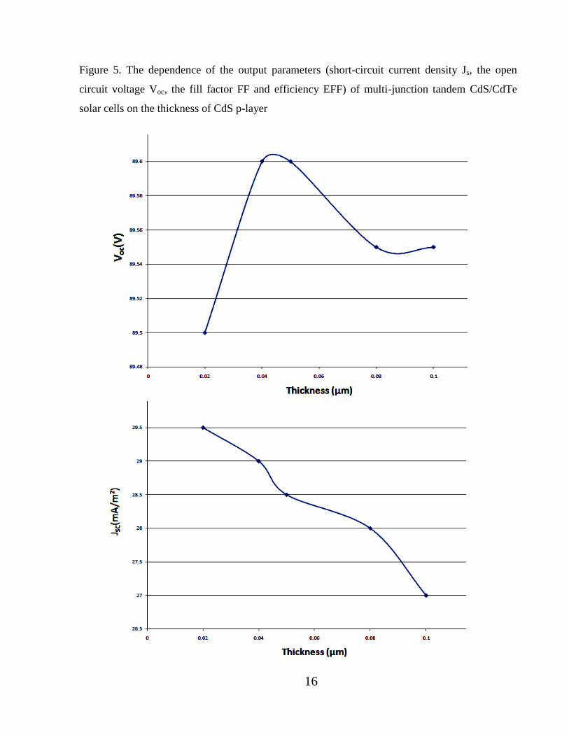
A) On the first stage in order to obtain more effective thickness of the top
layer of the CdS/CdTe solar cell, thickness of CdS p-layer was varied from 20 nm
to 100 nm. Since this layer is disposed on the top surface under the absorbent layer,
hence, it has a minimum thickness as compared with other layers. Thus the optimal
thickness of 50 nm for the layer, ensuring the highest efficiency was obtained.
ITO
(200
нm)
p- CdTe (50нm)
n- CdTe(200нm)
p- CdS (300нm)
n- CdS (1000нm)
Cu

15
Table 2 .: The parameters of the materials used in the simulation of the tandem multijunction CdS / CdTe solar cell
Materi
al
Band gap
(eV)
Conductivit
y type
Conduction
Band
Valence
Band
Electro
n
Affinity
(eV)
Electron
Mobility
(cm2 /v/s)
Hole
Mobility
(cm2 /v/s)
Free Carrier
Concentration (cm-3
)
Relative
Permittivit
y
ITO 3.60 N 2.0*1020 1.8*1019 4.10 50.0 70.0 1.0*1020 2.0
CdS 2.40 P 2.2*1018 1.8*1019 4.0 25.0 100.0 1.0*1016 10.0
CdS 2.40 N 2.2*1018 1.8*1019 4.0 25.0 100.0 1.1*1018 10.0
CdTe 1.50 P 8.0*1017 1.8*1019 3.90 40.0 320.0 2.0*1014 9.4
CdTe 1.50 N 8.0*1017 1.8*1019 3.90 40.0 320.0 2.0*1016 9.4
16
Figure 5. The dependence of the output parameters (short-circuit current density Js, the open
circuit voltage Voc, the fill factor FF and efficiency EFF) of multi-junction tandem CdS/CdTe
solar cells on the thickness of CdS p-layer

17

18
B) At the next stage the thickness of CdS p-layer was kept constant at 50
nm and the thickness of CdS n-layer was varied from 60 nm to 600 nm. Since this
layer is disposed on the CdTe p-layer and the CdS p-layer, it should have a
thickness less than the thickness of the lower layer, and greater than the thickness
of the top layer. Analysis of the results shows that the optimal thickness is 200 nm
as shown on the Figure 6.
At both stages of modeling the thickness of the CdTe n-layer was fixed and
equal to 3000 nm, and the thickness of the CdTe p-layer remained constant and
equal to 1000 nm. The results showed that the optimal efficiency of the tandem
multijunction CdS/CdTe solar cell with the above layer thicknesses equal to 31.8%,
i.e. efficiency of about two times greater than the same of the single-junction solar
cell, under the standard light spectrum of AM 1.5.

19
Figure 6. The dependence of the output parameters (short-circuit current density Js, the open
circuit voltage Voc, the filling factor FF and efficiency EFF) of tandem CdS/CdTe multijunction
solar cell on the thickness of CdS n-layer

20

21
CONCLUSION
Numerical simulation by means AMPS-1D shows that the highest
efficiency of single-junction CdS/CdTe solar cell, equal to 18.3%, achieved with a
CdTe layer thickness equal to 1000 nm and CdS layer thickness of 60 nm. This
result is in good agreement with the experimental data obtained by Chou et al.,
[17], where the maximum efficiency of CdS/CdTe solar cells was 17.3%.
On the basis of simulation single-junction solar cells we developed an
optimal structure of multi-junction tandem CdS/CdTe solar cell, and numerical
simulations show that its optimal efficiency in 31.8% can be obtained at the
thickness of CdS p-layer equal to 50 nm, and the thickness of the CdS n-layer of
200 nm, while we kept the fixed thickness of the CdTe n-layer of 3000 nm and
CdTe p-type layer, equal to 1000 nm.
LITERATURE
[1] Xuanzhi Wu.High-efficiency polycrystalline CdTe thin-film solar cells// Solar
Energy, 2004.-V. 77.- P. 803–814.
[2] Nowshad A., Akira Y., Makoto K. Effect of ZnTe and CdZnTe alloys at the
Back Contact of 1-μm Thick CdTe Thin Film Solar Cells // Japanese journal
of applied physics, 2002.-V.41.-N.5R.- P. 2834-2840.
[3] Sharafat H., Nowshad A., Matin M. A. A numerical study on the prospects of
high efficiency ultra thin ZnxCd1-xS/CdTe solar cell// Chalcogenide Letters,
2011.-vol. 8/- n. 3.- P. 263 – 272.
[4] Romeo A., Tiwari A.N., Zogg H. // Proceedings of the 2nd World Conference
and Exhibition on Photovoltaic Solar Energy Conversion,1998.- Vienna,
Austria.- P. 1105-1108.

22
[5] Tyan Y.S., Perez-Albuerne E.A.Efficient thin film CdS/CdTe solar cells//
Proceedings of 16th IEEE Photovoltaic Specialists Conference, IEEE
Publishing, New York, 1982.-P. 794-798.
[6] Ferekides C., Britt J., Ma Y., Killian L. High efficiency CdTe solar cells by
closespaced sublimation // Proceedings of 23rd IEEE Photovoltaic Specialists
Conference, New York, USA, 1993.- P. 389-393.
[7] Xuanzhi Wu.High-efficiency polycrystalline CdTe thin-film solar cells// Solar
Energy, 2004.-N. 77. - P. 803–814.
[8] Romeo N., Bosio A., Romeo A. An innovative process suitable to produce
high-efficiency CdTe/CdS thin-film modules // Solar Energy Materials &
Solar Cells, 2010.-V. 94.- N. 1.- p. 2–7.
[9] Ferekides C., Britt J., Ma Y., Killian L.High efficiency CdTe solar cells by
close spaced sublimation // in Proceedings of the 23rd IEEE Photovoltaic
Specialists Conference, 1993.-New York, USA.-P. 389 –393.
[10] Sharafat Hossain.MD, Nowahad. A, Razyokov.T .Prospects Of Back Contacts
with Back Surface Fields In High Efficiency ZnxCd1-xS/CdTe solar cells From
Numerical Modelling // Chalcogenide Letters,2011.-V. 8.- N. 3.- P. 199 – 210.
[11] Sharafat Hossain. MD, Nowahad A., Matin M.A. A Numerical Study on The
Prospects of High efficiency Ultra Thin ZnxCd1-xS/CdTe solar cell
//Chalcogenide Letters,2011.- V. 8.- N. 3.- P. 263 – 272.
[12] Wolden C.A., Kurtin J., Baxter J.B., Repins I., Shaheen S.E., Torvik J.T.,
Rockett A.A., Fthenakis V.M., Aydil E.S. Photovoltaic Manufacturing:
Present status, future prospects, and research needs/ J. Vac. Sci. Technol.,
2011.-V. 29 .-N.3.- P.1-16.
[13] Gessert T.A., Sheldon P., Li X., Dunlavy D., Niles D., Sasala R., Albright S.,
Zadler B. Studies of ZnTe Back Contacts to Cds/CdTe Solar Cells// 26th IEEE
PV Spec. Conf., 1997.- P.419-422.

23
[14] Romeo N., Bosio A., Canevari V., Podestà A. Recent progress on CdTe/CdS
thin film solar cells// Sol. Energy, 2004.-V. 77.- P. 795–801.
[15] Niemegeers A., Burgelman M. Effects of the Au/CdTe Back Contact on IV
and CV Characteristics of Au/CdTe/CdS/TCO Solar Cells // J. Appl.
Phys.1997.-V. 81.- N. 6.- P. 2881-2886.
[16] Gessert .T.A, Romero M.J., Dhere R.G., Asher S.E. Analysis of the ZnTe: Cu
Contact on CdS/CdTe Solar Cells// NREL Tech. Rep, 2003.-P.520-526.
[17] Chou H.C., Rohatgi A., Jokerst N.M., Thomas E.W., Kamra S. Copper
Migration in CdTe Heterojunction Solar Cells// J. Electr. Mater, 1996.-V. 25.-
N.7.-P.1093–1098.
[18] Gloeckler M., Fahrenbruch A.L., Sites J.R. Numerical Modeling of CIGS and
CdTe Solar Cells: Setting the Baseline // 3rd conf. on PV energy conv, 2003.-
P. 491 - 494.
[19] Brownson J.R.S., Georges C., Clement C.L. Synthesis of a δ-SnS Polymorph
by Electrodeposition // Chem. Mat. 2006 .-V.18. - P.6397-6402.
[20] Xuanzhi Wu.High-efficiency polycrystalline CdTe thin-film solar cells // Solar
Energy, 2004.-V. 77.- P. 803–814.
[21] Nowshad A., Kamaruzzaman S.,Makoto K.Numerical modeling of CdS/CdTe
and Cds/CdTe/ZnTe solar cells as a function of CdTe thickness // Solar
Energy Materials and Solar Cells, 2007.-V. 91.- N.13.- P. 1202-1208.
[22] Nowshad A., Kamaruzzaman S., Yahya M., Zaharim A. Significance of
Absorber Thickness Reduction in CdTe Thin Film Solar Cells for Promising
Terrestrial Usage – From the Perspective of Numerical Analysis// Proceedings
of the 8th
WSEAS International Conference on POWER SYSTEMS (PS
2008).- P.299-305.
[23] Nowshad A., Isaka T., Okamoto T., Yamada A., Konagai M. Prospect of
Thickness Reduction of the CdTe Layer in Highly Efficient CdTe Solar cells
24
Towards 1μm // Japanese Journal of Applied Physics,1999.-V. 38 .-N.8R.- P.
4666-4670.
[24] http://www.pveducation.org/pvcdrom/solar-cell-operation/tandem-cells
Copyright © 2022 FDOKUMEN