Electroless Deposition of CdTe on Stainless Steel 304 ...
101
Electroless Deposition of CdTe on Stainless Steel 304 Substrates By James Francis Malika Submitted in Partial Fulfillment of the Requirements for the Degree of Master of Science in the Chemistry Program YOUNGSTOWN STATE UNIVERSITY May 2021
-
Upload
khangminh22 -
Category
Documents
-
view
0 -
download
0
Transcript of Electroless Deposition of CdTe on Stainless Steel 304 ...
Electroless Deposition of CdTe on Stainless Steel 304 Substrates
By James Francis Malika
Submitted in Partial Fulfillment of the Requirements
for the Degree of
Master of Science
in the
Chemistry
Program
YOUNGSTOWN STATE UNIVERSITY
May 2021

Electroless Deposition of CdTe on Stainless Steel 304 Substrates
James Francis Malika
I hereby release this thesis to the public. I understand that this thesis will be made available from the Ohio LINK ETD Center and the Maag Library Circulation Desk for public access. I also authorize the University or other individuals to make copies of this thesis as needed for scholarly research. Signature: James Francis Malika, Student Date Approvals: Dr. Clovis A. Linkous, Thesis Advisor Date Dr. Timothy R. Wagner, Committee Member Date Dr. Christopher Arnsten, Committee Member Date Dr. Salvatore A. Sanders, Dean of Graduate Studies Date

iii
ABSTRACT
The semiconductor cadmium telluride (CdTe) has become the leading material for thin-
film photovoltaic applications. Among the many techniques for preparing these thin
films, electroless deposition, commonly known as chemical bath deposition, deserves
special focus since it has been shown to be a pollution-free, low-temperature and
inexpensive method. In this project, CdTe thin films were deposited on stainless steel 304
by the electroless deposition method using cadmium acetate and tellurium oxide
dissolved in pH 12.5 NH3(aq). The deposition was based on the gradual release of
cadmium ions (Cd2+) and the gradual addition of tellurium as TeO32- and their subsequent
reduction in a hot aqueous alkaline chemical bath at 70 oC. This was attained by adding a
complexing agent such as ammonia and a chemical reducing agent. Using
triethanolamine as a complexing agent produced similar results. The following reducing
agents were used: aluminum, sodium hypophosphite, formaldehyde, sodium borohydride
and hydrazine. All of them deposited a film on stainless steel containing Cd and Te, but
formaldehyde produced the best films in terms of uniform thickness, photosensitivity,
and rapid growth rate. Electroless deposition of a thin Pt layer on top of the CdTe film
improved the cathodic CdTe polarization for hydrogen evolution. The structural and
morphological properties of the resulting films were characterized using X-ray diffraction
(XRD), stylus profilometry, scanning electron microscopy (SEM) and energy dispersive
X-ray spectroscopy (EDS) while the light/dark voltametric methods were used to
determine the films’ photosensitivity.

iv
ACKNOWLEDGEMENT
I would like to appreciate the help of several individuals who have assisted me in various
aspects of this thesis and the work relating to it. First, I would like to express my sincere
gratitude to my research advisor, Dr. Clovis A. Linkous for the continuous support of my
study and research, for his patience, motivation, enthusiasm, and immense knowledge. I
would like to thank you so much for supervising the research which has led up to this
document and for the countless insights which were extended to me through regular visits
to your office. I would also like to thank Dr. Christopher Arnsten for the time,
supervision, and direction he has given to the research behind this thesis as well as the
thesis itself. Dr. Timothy Wagner, thanks for guiding me in many of the improvements
that have been made to this document. I would also like to thank Ray Hoff for helping me
with the instruments. I would love to thank my family for their support too. A special
thanks to fellow students Bansah, Kim, Omweri and Audrey without whom nothing much
would have been done. I am deeply grateful to the Chemistry Department too for giving
me a chance to study and do this project here.
v
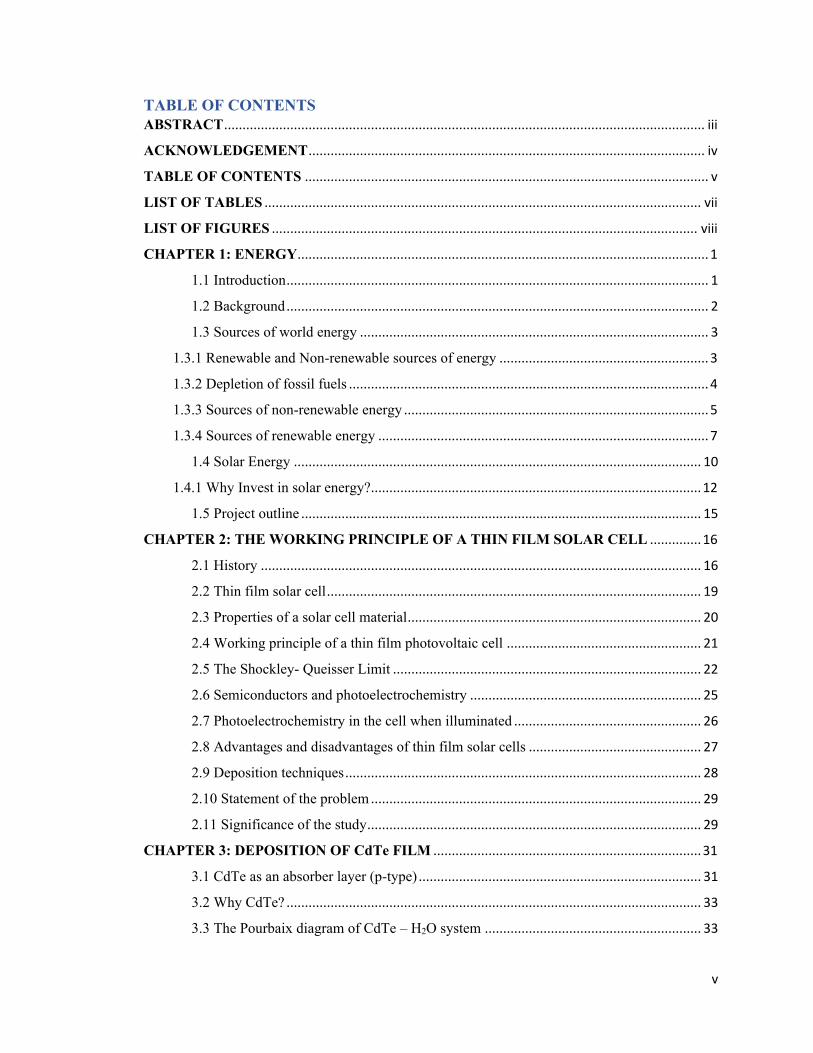
TABLE OF CONTENTS ABSTRACT ................................................................................................................................... iii
ACKNOWLEDGEMENT ............................................................................................................ iv
TABLE OF CONTENTS .............................................................................................................. v
LIST OF TABLES ....................................................................................................................... vii
LIST OF FIGURES .................................................................................................................... viii
CHAPTER 1: ENERGY ................................................................................................................ 1
1.1 Introduction ................................................................................................................... 1
1.2 Background ................................................................................................................... 2
1.3 Sources of world energy ............................................................................................... 3
1.3.1 Renewable and Non-renewable sources of energy ......................................................... 3
1.3.2 Depletion of fossil fuels .................................................................................................. 4
1.3.3 Sources of non-renewable energy ................................................................................... 5
1.3.4 Sources of renewable energy .......................................................................................... 7
1.4 Solar Energy ............................................................................................................... 10
1.4.1 Why Invest in solar energy?.......................................................................................... 12
1.5 Project outline ............................................................................................................. 15
CHAPTER 2: THE WORKING PRINCIPLE OF A THIN FILM SOLAR CELL .............. 16
2.1 History ........................................................................................................................ 16
2.2 Thin film solar cell ...................................................................................................... 19
2.3 Properties of a solar cell material ................................................................................ 20
2.4 Working principle of a thin film photovoltaic cell ..................................................... 21
2.5 The Shockley- Queisser Limit .................................................................................... 22
2.6 Semiconductors and photoelectrochemistry ............................................................... 25
2.7 Photoelectrochemistry in the cell when illuminated ................................................... 26
2.8 Advantages and disadvantages of thin film solar cells ............................................... 27
2.9 Deposition techniques ................................................................................................. 28
2.10 Statement of the problem .......................................................................................... 29
2.11 Significance of the study ........................................................................................... 29
CHAPTER 3: DEPOSITION OF CdTe FILM ......................................................................... 31
3.1 CdTe as an absorber layer (p-type) ............................................................................. 31
3.2 Why CdTe? ................................................................................................................. 33
3.3 The Pourbaix diagram of CdTe – H2O system ........................................................... 33
vi
3.4 Electroless deposition technique ................................................................................. 35
3.4.1 Literature review on electroless deposition .................................................................. 37
3.4.2 Why electroless deposition? ......................................................................................... 37
3.4.3 Drawbacks of electroless deposition ............................................................................. 38
3.4.4 Components of electroless deposition ........................................................................... 38
3.4.5 Reducing agents and ligands. ........................................................................................ 39
CHAPTER 4: EXPERIMENTAL DETAILS ............................................................................ 42
4.1 Substrate cleaning process .......................................................................................... 42
4.2 Chemical components ................................................................................................. 43
4.3 Procedure .................................................................................................................... 44
4.4 Apparatus for determining surface morphology. ........................................................ 49
4.5 Apparatus for measuring CdTe film thickness ........................................................... 50
4.5.1 Scanning electron microscopy (SEM) .......................................................................... 50
4.5.2 Profilometer .................................................................................................................. 51
4.6 Apparatus for structural analysis ................................................................................ 52
4.6.1 Powder X-ray diffractometer ........................................................................................ 52
4.7 Electrochemistry and photovoltaic measurements ...................................................... 53
4.7.1 Potentiostat .................................................................................................................... 54
CHAPTER 5: RESULTS AND DISCUSSION-CdTe Thin Film Characterization .............. 55
5.1 Growth mechanism ..................................................................................................... 55
5.2 Photographs of the CdTe thin films obtained. ............................................................ 56
5.3 Scanning electron microscopy (SEM) ........................................................................ 58
5.4 SEM-EDS measurements for elemental composition ................................................. 61
5.5 Film thickness using a scanning electron microscopy (SEM) .................................... 64
5.6 Film thickness using a stylus profilometer. ................................................................ 65
5.7 X-Ray Diffraction (XRD) for structural analysis ....................................................... 68
5.8 Photoelectrochemical measurements/Cyclic voltammetry (CV) ................................ 76
5.9 Photoelectrochemical measurements/Linear sweep voltammetry (LSV) ................... 78
CHAPTER 6: CONCLUSION AND FUTURE WORK .......................................................... 82
6.1 Conclusion .................................................................................................................. 82
6.2 Future work ................................................................................................................. 83
REFERENCES ............................................................................................................................. 84

vii
LIST OF TABLES
Table 1: Non-renewable energy sources, merits, and demerits ...........................................5
Table 2: Renewable energy sources, merits, and demerits. .................................................8
Table 3: Thin film deposition methods. .............................................................................29
Table 4: Properties of CdTe. ..............................................................................................32
Table 5: Properties of some reducing agents ....................................................................40
Table 6: List of chemicals/materials used ..........................................................................44
viii
LIST OF FIGURES
Figure 1: Estimated length of time left for fossil fuels ........................................................5
Figure 2: Solar radiation spectrum. ....................................................................................11
Figure 3: Largest array of solar panels in the US as of 2014: Agua Caliente, Yuma
county, AZ showing how solar energy is harnessed from the sun. ....................................12
Figure 4: Global photovoltaics (PV) capacity in gigawatts (GW) between years 2000 and
2015.13 ................................................................................................................................14
Figure 5: Different solar cell generations. .........................................................................18
Figure 6: Structure of a CdTe thin film solar cell. .............................................................20
Figure 7: Working principle of photovoltaic cell. .............................................................21
Figure 8: A Shockley Queisser efficiency curve. ..............................................................23
Figure 9: A I-V relationship of a solar cell. .......................................................................24
Figure 10: Representation of bands, band gaps and physical properties. ..........................26
Figure 11: SEM image of unannealed electrodeposited CdTe film (×2500). ...................30
Figure 12: SEM image of annealed electrodeposited CdTe film at 350 oC under Ar
(×3500). ..............................................................................................................................30
Figure 13: Arrangement of the photovoltaic (PV) cell based on CdTe as an absorber layer
............................................................................................................................................31
Figure 14: Unit cell crystal structure of CdTe. ..................................................................32
Figure 15: Equilibrium potential–pH (Pourbaix) diagram of the CdTe–H2O system. ......35
Figure 16: A schematic diagram representing the ELD process. .......................................39
Figure 17: An illustration of the electroless deposition technique. ...................................41
Figure 18: Cleaned and dried out SS 304 substrates..........................................................43

ix
Figure 19: Electric tape attached at the rear side of the substrate. .....................................43
Figure 20: Set up of the experiment conducted in the 1st approach. ..................................46
Figure 21: Set up of the experiment conducted in the 2nd approach. .................................48
Figure 22: A temperature-controlled furnace, (MODEL RTP-300 RAPID THERMAL
PROCESSOR). ..................................................................................................................49
Figure 23: Picture of a scanning electron microscope ((JEOL JIB-4500). ........................50
Figure 24: A SEM sample holder for determining film thickness. ....................................50
Figure 25: A stylus profilometer for measuring film thickness. ........................................51
Figure 26: The YSU version of XRD used for analysis. ...................................................53
Figure 27: Image of stainless steel 304 substrate (uncoated sample). ...............................56
Figure 28: Images of CdTe films coated on stainless steel prepared from Approach I (Al
as the reducing agent). .......................................................................................................56
Figure 29: Images of CdTe films coated on stainless steel prepared from Approach II
(hydrazine hydrate as the reducing agent). ........................................................................56
Figure 30: Images of CdTe films coated on stainless steel prepared from Approach II
(sodium hypophosphite as the reducing agent). .................................................................57
Figure 31: Images of CdTe films coated on stainless steel prepared from Approach II
(sodium borohydride as the reducing agent). .....................................................................57
Figure 32: Images of CdTe films coated on stainless steel prepared from Approach II
(formaldehyde as the reducing agent). ...............................................................................57
Figure 33: SEM image of stainless Steel 304 (uncoated sample) ......................................58
Figure 34: SEM images of as deposited and annealed (350 oC) CdTe films prepared from
Approach I (Al as the reducing agent). ..............................................................................59

x
Figure 35: SEM images of as deposited and annealed (350 oC) CdTe films prepared from
Approach II (hydrazine hydrate as the reducing agent). ....................................................59
Figure 36: SEM images of as deposited and annealed (350 oC) CdTe films prepared from
Approach II (sodium hypophosphite as the reducing agent). ............................................60
Figure 37: SEM images of as deposited and annealed (350 oC) CdTe films prepared from
Approach II (sodium borohydride as the reducing agent). ................................................60
Figure 38: SEM images of as deposited and annealed (350 oC) CdTe films prepared from
Approach II (formaldehyde as the reducing agent). ..........................................................61
Figure 39: SEM-EDS pattern of stainless steel 304 (uncoated sample). ...........................62
Figure 40: SEM-EDS pattern of CdTe films coated on stainless steel prepared from
Approach I (Al as the reducing agent). ..............................................................................62
Figure 41: SEM-EDS pattern of CdTe films coated on stainless steel prepared from
Approach II (hydrazine hydrate as the reducing agent). ....................................................63
Figure 42: SEM-EDS pattern of CdTe films coated on stainless steel prepared from
Approach II (sodium hypophosphite as the reducing agent). ............................................63
Figure 43: SEM-EDS pattern of CdTe films coated on stainless steel prepared from
Approach II (sodium borohydride as the reducing agent). ................................................64
Figure 44: SEM-EDS pattern of CdTe films coated on stainless steel prepared from
Approach II (formaldehyde as the reducing agent). ..........................................................64
Figure 45: SEM film thickness image of annealed (350 oC) CdTe films prepared from
Approach I (Al as the reducing agent). ..............................................................................65
Figure 46: SEM film thickness image of annealed (350 oC) CdTe films prepared from
Approach II (hydrazine hydrate as the reducing agent). ....................................................65

xi
Figure 47: Profilometry measurement of CdTe film thickness prepared from Approach I
(Al as the reducing agent). .................................................................................................66
Figure 48: Profilometry measurement of CdTe film thickness prepared from Approach II
(hydrazine hydrate as the reducing agent). ........................................................................66
Figure 49: Profilometry measurement of CdTe film thickness prepared from Approach II
(sodium hypophosphite as the reducing agent). .................................................................67
Figure 50: Profilometry measurement of CdTe film thickness prepared from Approach II
(sodium borohydride as the reducing agent). .....................................................................67
Figure 51: Profilometry measurement of CdTe film thickness prepared from Approach II
(formaldehyde as the reducing agent). ...............................................................................68
Figure 52: XRD pattern of uncoated stainless steel 304 substrates. ..................................69
Figure 53: XRD pattern for the unannealed CdTe films and the SS 304 substrate. ..........70
Figure 54: XRD pattern for the annealed CdTe films and the SS 304 substrate. ..............70
Figure 55: XRD pattern of CdTe film (as deposited) coated on SS 304 substrate prepared
from Approach I (Al as the reducing agent). .....................................................................71
Figure 56: XRD pattern of CdTe film (annealed) coated on SS 304 substrate prepared
from Approach I (Al as the reducing agent). .....................................................................71
Figure 57: XRD pattern of CdTe film (as deposited) coated on SS 304 substrate prepared
from Approach II (hydrazine as the reducing agent). ........................................................72
Figure 58: XRD pattern of CdTe film (annealed) coated on SS 304 substrate prepared
from Approach II (hydrazine as the reducing agent). ........................................................72
Figure 59: XRD pattern of CdTe film (as deposited) coated on SS 304 substrate prepared
from Approach II (sodium hypophosphite as the reducing agent). ...................................73
xii
Figure 60: XRD pattern of CdTe film (annealed) coated on SS 304 substrate prepared
from Approach II (sodium hypophosphite as the reducing agent). ...................................73
Figure 61: XRD pattern of CdTe film (as deposited) coated on SS 304 substrate prepared
from Approach II (formaldehyde as the reducing agent). ..................................................74
Figure 62: XRD pattern of CdTe film (annealed) coated on SS 304 substrate prepared
from Approach II (formaldehyde as the reducing agent). ..................................................74
Figure 63: XRD pattern of CdTe film (as deposited) coated on SS 304 substrate prepared
from Approach II (sodium borohydride as the reducing agent). .......................................75
Figure 64: XRD pattern of CdTe film (annealed) coated on SS 304 substrate prepared
from Approach II (sodium borohydride as the reducing agent). .......................................75
Figure 65: XRD pattern of CdTe commercial powder. .....................................................76
Figure 66: Cyclic voltammogram of SS 304-Control in the dark/light (1 M H2SO4,
Ag/AgCl reference electrode at 25 oC, scan rate 50 mV/s). ..............................................77
Figure 67: Cyclic voltammogram of CdTe/SS 304 in the light/dark (1 M H2SO4, Ag/AgCl
reference electrode at 25 oC, scan rate 50 mV/s, formaldehyde as the reducing agent). ...77
Figure 68: Cyclic voltammetry of Pt/CdTe/SS 304 in the light/dark (1 M H2SO4,
Ag/AgCl reference electrode at 25 oC, scan rate 50 mV/s, formaldehyde as the reducing
agent)..................................................................................................................................78
Figure 69: Linear sweep voltammetry of blank SS 304 in the dark/light (1 M H2SO4,
Ag/AgCl reference electrode at 25 oC, scan rate 5 mV/s, from -1.0 V to 0.0 V). .............79
Figure 70: Linear sweep voltammetry of CdTe coated film in the dark/light (1 M H2SO4,
Ag/AgCl reference electrode at 25 oC, scan rate 5 mV/s, from -1.0 V to 0.0 V, Al as the
reducing agent). ..................................................................................................................79

xiii
Figure 71: Linear sweep voltammetry of CdTe coated film in the dark/light (1 M H2SO4,
Ag/AgCl reference electrode at 25 oC, scan rate 5 mV/s, from -1.0 V to 0.0 V, NaH2PO2
as the reducing agent). .......................................................................................................80
Figure 72: Linear sweep voltammetry of CdTe coated film in the dark/light (1 M H2SO4,
Ag/AgCl reference electrode at 25 oC, scan rate 5 mV/s, from -1.0 V to 0.0 V, hydrazine
as the reducing agent). .......................................................................................................80
Figure 73: Linear sweep voltammetry of CdTe coated film in the dark/light (1 M H2SO4,
Ag/AgCl reference electrode at 25 oC, scan rate 5 mV/s, from -1.0 V to 0.0 V,
formaldehyde as the reducing agent). ................................................................................81
Figure 74: Linear sweep voltammetry of CdTe coated film in the dark/light (1 M H2SO4,
Ag/AgCl reference electrode at 25 oC, scan rate 5 mV/s, from -1.0 V to 0.0 V, NaBH4 as
the reducing agent). ............................................................................................................81

1
CHAPTER 1: ENERGY 1.1 Introduction
Renewable energy is often defined as the energy that is obtained from renewable
resources. These resources are naturally replaced on a human timescale. These resources
include: carbon neutral sources like solar, wind, rain, ocean tides, geothermal heat and
ocean waves. Renewable energy sources occur over a wider geographical area unlike
other energy resources which are unevenly distributed in a few countries. Speedy
development of renewable energy sources and energy efficiency technologies would
bring about significant energy security, climate change mitigation and economic benefits.
This would also minimize environmental pollution like air pollution caused by
combustion of fossil fuels and improve public health by reducing premature mortalities
caused by pollution.1
A vital source of renewable energy is the energy sourced from the sun. This energy is
tapped by a wide range of ever-evolving technologies like photovoltaics, solar
architecture, and artificial photosynthesis.2 A photovoltaic (PV) or solar cell, is an
electrical device that can convert sunlight into direct current by a physical phenomenon
called photovoltaic effect.
Solar cells are named depending on the kind of semiconductor material used in making
them. The materials have certain properties in them that enable sunlight absorption. Solar
cells are made to suit where they got to be used. Some are designed to absorb sunlight on
the Earth's surface whereas others are designed to be used in space applications. Solar
cells can be single-junction or multi-junctions to maximize solar absorption and charge
separation mechanisms.3
2
A thin-film solar cell is a 2nd generation PV cell that is made by coating one or more thin
layers of a photovoltaic material on the surface of a substrate, like plastic, glass, or metal.
These solar devices, which are commercially utilized in many applications, include
cadmium telluride (CdTe), copper indium gallium diselenide (CIGS) and amorphous
thin-film silicon (a-Si, TF-Si). Cadmium telluride thin films accounts for more than half
of the thin film market. The cell's lab efficiency has increased significantly over the years
just like CIGS thin films and its efficiency is almost close to that of polycrystalline
silicon.1
CdTe is preferred as a thin solar photovoltaic material due to its 1.5 eV band gap. This is
closer to the maximum PV efficiency band gap of 1.34 eV according to the Schockley-
Quiesser efficiency curve. This makes it well-conformed to the solar spectrum and nearly
optimal for the conversion of sunlight into electric current by a single junction. That is
why we choose CdTe thin film deposition on a stainless steel 304 substrate using
electroless deposition process at optimum growth conditions.
1.2 Background
Energy, as part of physics, is defined as: “the ability to do work”. It may occur in many
forms including but not limited to potential, kinetic, thermal, electrical, chemical, and
nuclear. There are, moreover, heat and work—i.e., energy in the process of transfer from
one body to another. After it has been transferred, energy is always designated according
to its nature. Hence, heat transferred may become thermal energy, while work done may
manifest itself in the form of mechanical energy.4 Energy therefore cannot naturally be
created nor destroyed but it can only be transformed from one form to another.
3
Energy access is a critical enabler of access to the basic needs and essential services
which are supplied through other sectors of the economy namely agriculture, health,
education, water, transport, construction, to mention but a few. As such, it is extremely
vital to the lifespan of these sectors without which the livelihoods and quality of life of
many are consequently affected. Energy is the engine for economic growth for any
society or country as it provides the basis for socio-economic development.5
Lack of access to modern energy, makes it impossible to attain Sustainable Millennium
Development Goals. The United Nations advocates for all, to access low cost, reliable,
sustaining, and modern energy.
1.3 Sources of world energy
Fossil fuels based on coal, petroleum and natural gas cannot be replenished and they have
been a major source of world energy and accounts for about 85% of the world’s primary
energy consumption. The consumption of energy across the globe is on the rise because
of increased population thereby, straining the already available energy sources.
1.3.1 Renewable and Non-renewable sources of energy
Renewable energy resources are infinite energy sources that quickly replenish themselves
and can be used repeatedly. Examples of renewable energy sources include solar, wind,
biogas, among others. Non-renewable energy cannot be regenerated and include fossil fuels
based on coal, petroleum, and natural gas. A fossil fuel is formed by natural processes like
anaerobic decomposition of buried dead organic matter, containing organic molecules
originating from ancient photosynthesis that produce energy when they burn. Fossil fuels

4
face depletion someday, hence, are non-renewable. When these fuels are burned, they
generate greenhouse gases, making their overreliance unsustainable.6
1.3.2 Depletion of fossil fuels
Fossil fuels, majorly coal, oil, and gas are finite and when consumed for a long time, their
deposits will eventually get depleted. There are some concerns about this risk which have
lasted for years. This is better explained by Hubbert’s Peak Theory — also known as the
Hubbert curve. In 1956, M. King Hubbert published his hypothesis that for any given
region, a fossil fuel production curve would be in the form of a bell-shaped curve, with
production hiking following discovery of new resources and improved extraction
techniques, attaining a peak, then eventually declines as resources became used up.7
Estimates suggest that if the world’s fuel consumption continues at the present rate, then
oil and gas reserves may get depleted within our lifetimes. Coal is estimated to last longer.
Figure 1 below shows a graph of estimated length of time left for conventional fossil fuels
as of 2015.

5
Time in Years
Figure 1: Estimated length of time left for fossil fuels7
1.3.3 Sources of non-renewable energy
These are energy sources that are limited in nature and once used cannot be replenished
again. Table 1.1 below represents non-renewable energy sources, merits, and their
demerits.
Table 1: Non-renewable energy sources, merits, and demerits
Type of fuel
Source Merits Demerits
Oil They are formed from the remains of animals, buried underground and that that lived millions of years ago.
Oil is ready- made fuel. It is relatively inexpensive to tap and get converted into useful energy.
Oils are limited in supply and face depletion. When they undergo combustion,

6
they emit atmospheric pollutants as well as greenhouse gases.
Coal They are formed from the remains of plants, buried underground and that that lived millions of years ago.
Coal supplies are estimated to last longer than oil or gas. Coal is ready made fuel which is readily mined and easily converted into useful energy.
Coal reserves are limited in supply and face depletion. When they undergo combustion, they emit atmospheric pollutants as well as greenhouse gases.
Natural gas
Conventional natural gas is found embedded into porous and permeable bedrocks or mixed into oil reservoirs and then can be tapped by standard drilling.
Relatively greener form of energy than oil and coal. It is ready-made fuel and slightly cheaper to harness and to convert into energy.
Natural gas reserves are limited in supply and face depletion. When they undergo combustion, they emit atmospheric pollutants as well as greenhouse gases.
Nuclear Obtained from reactions taking place from within the nucleus of atoms such as: nuclear fission, nuclear decay, and nuclear fusion. Most of the electricity from nuclear energy is sourced
Have a high heating value-a small radioactive material emits a lot of energy. Does not produce atmospheric pollutants.
Despite being relatively cheap to operate, nuclear power plants are incredibly expensive to

7
from nuclear fission of uranium and plutonium.
Cheaper raw materials that can last a very long period.
build. Can cause accidents if not properly handled. Produces radioactive waste that have adverse effects to humanity and the environment. Nuclear weapons pose a security threat. Limited Fuel Supply.
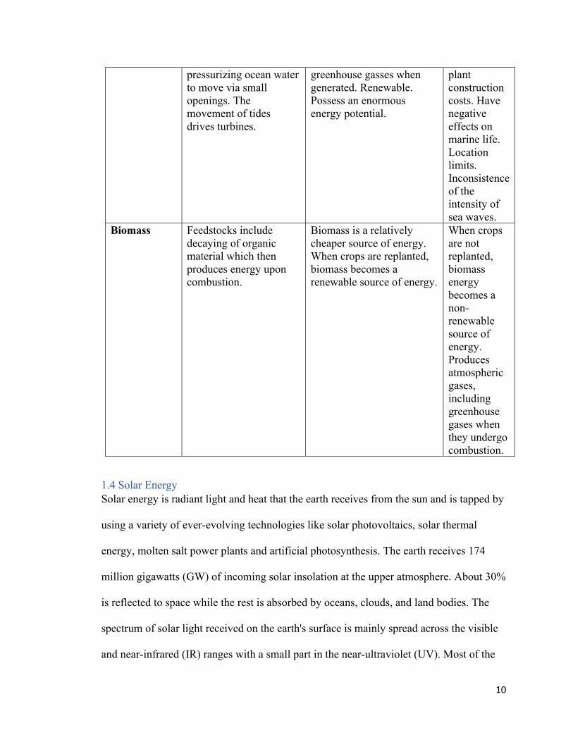
Biomass Feedstocks include dedicated energy and agricultural crop residues, residues from forests, algae, residues from wood processing mills, and municipal and wet wastes.
It is a relatively cheaper energy source. When crops are replanted, then biomass becomes a renewable source of energy.
If crops are not replanted, then biomass becomes a non-renewable source of energy. Produces atmospheric gases, including greenhouse gases when they undergo combustion.
1.3.4 Sources of renewable energy
These are sources of energy that replenish themselves and can be used repeatedly. Table
1.2 below shows renewable sources of energy, merits, and their demerits.

8
Table 2: Renewable energy sources, merits, and demerits.
Type of fuel Source Merits Demerits Solar Radiant light and heat
from the sun that is tapped by using a variety of ever-evolving technologies like solar photovoltaics, solar thermal energy, molten salt power plants and artificial photosynthesis.8
Solar power is a green, clean, pollution free and does not emit greenhouse gases when installed. It is infinite source of energy
The initial cost of solar panel installation is high. Solar PV panels require a lot of space. Solar energy storage is expensive. Solar panels depend on sunlight to effectively harness solar energy.
Wind Wind turbines convert wind energy into electricity
Infinite energy supply Wind power is inexpensive. It is a clean fuel source.
Wind turbines cause noise pollution. The wind flow can be inconsistent. Wind turbines require high initial cost of installation and can use a large piece of land.
Geothermal Sourced from volcanic regions when magma heats nearby rocks and underground aquifers. Hot water can then be released through underground outlets through geysers, hot springs, steam vents and
It is a potentially an infinite source of energy. Environmentally friendly. Possesses a huge potential. Does not require fuel to run.
Geothermal energy has high startup capital costs. May release harmful gases. Suited to a particular

9
underwater vents. The heat can be harnessed and used directly to generate electricity.
region experiencing a volcanic activity. Geothermal sites may experience a dry spell leaving power stations inactive.
Hydroelectric Power (HEP)
Energy tapped when water moves through lakes, rivers, and dams.
Fueled by water, hence a clean source of energy therefore it is a non-pollutant.
It is expensive to install a HEP Surrounding communities and landscapes can be prone to flooding. Dams can have adverse ecological impacts.
Wave Wave energy or power is the capturing and transport of energy by movement of ocean surface waves.
Have zero emissions - wave energy does not emit greenhouse gasses when generated. Renewable. Possess an enormous energy potential. Reliable energy source.
Suitable to Certain Locations which have proximity to water bodies. Have negative effects on marine ecosystem. Serves as a source of disturbance for private and commercial water vessels.
Tidal A tidal barrage is built across estuaries
Have zero emissions - wave energy does not emit
Initial high tidal power
10
pressurizing ocean water to move via small openings. The movement of tides drives turbines.
greenhouse gasses when generated. Renewable. Possess an enormous energy potential.
plant construction costs. Have negative effects on marine life. Location limits. Inconsistence of the intensity of sea waves.
Biomass Feedstocks include decaying of organic material which then produces energy upon combustion.
Biomass is a relatively cheaper source of energy. When crops are replanted, biomass becomes a renewable source of energy.
When crops are not replanted, biomass energy becomes a non-renewable source of energy. Produces atmospheric gases, including greenhouse gases when they undergo combustion.
1.4 Solar Energy Solar energy is radiant light and heat that the earth receives from the sun and is tapped by
using a variety of ever-evolving technologies like solar photovoltaics, solar thermal
energy, molten salt power plants and artificial photosynthesis. The earth receives 174
million gigawatts (GW) of incoming solar insolation at the upper atmosphere. About 30%
is reflected to space while the rest is absorbed by oceans, clouds, and land bodies. The
spectrum of solar light received on the earth's surface is mainly spread across the visible
and near-infrared (IR) ranges with a small part in the near-ultraviolet (UV). Most of the

11
world's population live in areas with insolation levels of 150–300 watts/m2, or 3500–7000
watt-hour/m2 per day.9Figure 2 below shows the solar radiation spectrum with the sun.
Being a radiant source of energy, it behaves like a black body radiator at about 5900 K
and the spectral distribution is estimated as follows: 8% ultraviolet, 44% visible and 48%
infrared radiation. The solar constant I0, which is the intensity of solar radiation just
outside the Earth's atmosphere, is equivalent to 1.37 kW/m2.
Figure 2: Solar radiation spectrum.10
Solar energy is absorbed by the Earth's land mass, oceans, and atmosphere. Warm air
containing water vapor from the water bodies rises, causing atmospheric convection. On
reaching the upper atmosphere, water vapor condenses into clouds because the

12
temperature is quite low and then falls back as rain onto the Earth's surface therefore
completing the water cycle.
The latent heat of condensation of water maximizes convection and then leads to
atmospheric occurrences like wind, cyclones, and anticyclones. Solar radiation absorbed
by water and land bodies keep the surface of the earth at a temperature of about 14 °C.
When green plants make their own food by a process called photosynthesis, they convert
energy from the sun into chemically stored energy, then produces food, wood and
biomass from which fossil fuels are derived.11 The sun will be here for the next 5 billion
years and it can produce about 3,850,000 exajoules (EJ) of energy per year. This energy
is about 7700 times more than what is consumed by human activity on earth. Studies
have been conducted with the aim of finding a way to harness and convert solar energy
and then store it for future use.12 Figure 3 below shows the 8th largest array of solar
panels in the world and 3rd globally based on CdS/CdTe cells as of 2014.
Figure 3: Largest array of solar panels in the US as of 2014: Agua Caliente, Yuma
county, AZ showing how solar energy is harnessed from the sun.
1.4.1 Why Invest in solar energy? Photovoltaics, which has enabled the tapping of solar energy, has several advantages: It
does not pollute the environment and greenhouse gases are not emitted after installation;
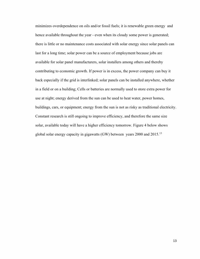
13
minimizes overdependence on oils and/or fossil fuels; it is renewable green energy and
hence available throughout the year - even when its cloudy some power is generated;
there is little or no maintenance costs associated with solar energy since solar panels can
last for a long time; solar power can be a source of employment because jobs are
available for solar panel manufacturers, solar installers among others and thereby
contributing to economic growth. If power is in excess, the power company can buy it
back especially if the grid is interlinked; solar panels can be installed anywhere, whether
in a field or on a building; Cells or batteries are normally used to store extra power for
use at night; energy derived from the sun can be used to heat water, power homes,
buildings, cars, or equipment; energy from the sun is not as risky as traditional electricity.
Constant research is still ongoing to improve efficiency, and therefore the same size
solar, available today will have a higher efficiency tomorrow. Figure 4 below shows
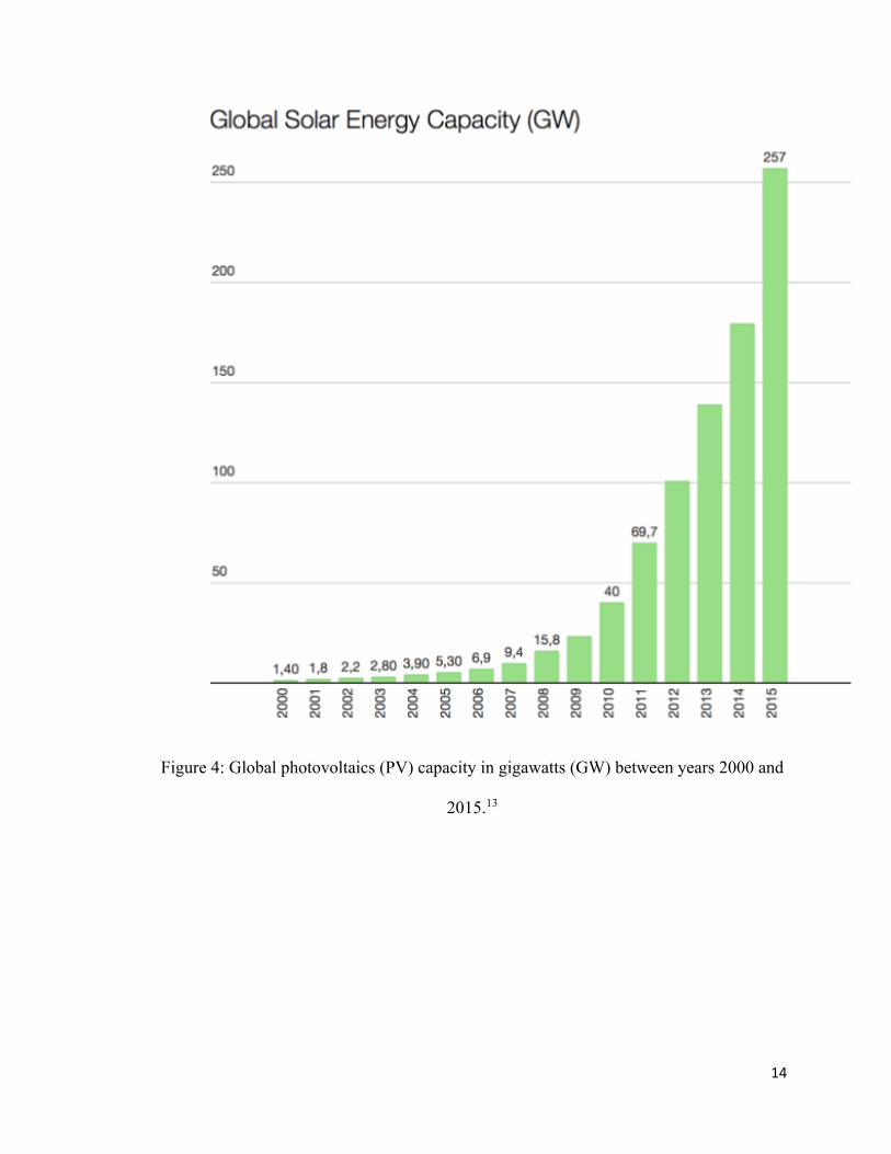
global solar energy capacity in gigawatts (GW) between years 2000 and 2015.13
14
Figure 4: Global photovoltaics (PV) capacity in gigawatts (GW) between years 2000 and
2015.13

15
1.5 Project outline Chapter 1: This chapter briefly outlines renewable and non-renewable sources of energy
and highlights on some of the reasons why investing in solar energy is a better option as
compared to other energy sources.
Chapter 2: This chapter describes the working principle of a thin film solar cell.
Chapter 3: This chapter describes CdTe deposition by electroless deposition using
various reducing agents and complexing agents.
Chapter 4: This chapter gives descriptions of the experimental details.
Chapter 5: This chapter gives a description of the results and discussion.
Chapter 6: Conclusions and future works are briefly outlined in this chapter.
16
CHAPTER 2: THE WORKING PRINCIPLE OF A THIN FILM SOLAR CELL 2.1 History
At the age of 19, in 1839, a French physicist called Edmond Becquerel did an experiment
to demonstrate the Photovoltaic Effect. He designed the world’s 1st PV cell in his father’s
laboratory. In 1873, Willoughby Smith became the 1st person to describe the effect of
light on selenium when an electric current is passed. Charles Fritts built the first solid
state photovoltaic cell in 1883 when he coated selenium with a thin layer of gold-his
device had efficiency of about 1%. In 1888, a Russian physicist named Aleksandr
Stoletov built the first cell which was based on the photoelectric effect which had been
discovered in 1887 by Heinrich Hertz. Albert Einstein in 1905, proposed a new quantum
theory of light and explained the photoelectric effect in a landmark paper for which he
won the Nobel Prize in 1921. In 1941 Vadim Lashkaryov discovered p-n junctions of
copper oxide and silver sulfide photocells.1 In 1946, Russel Ohl patented the modern
junction semiconductor solar cell. On the 25th of April,1954, the first practical PV cell
was demonstrated in public at Bell laboratories, New Jersey by Daryl Chapin, Calvin S.
Fuller and Gerald Pearson.6
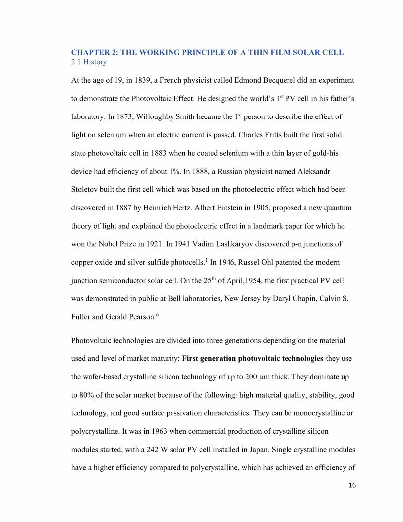
Photovoltaic technologies are divided into three generations depending on the material
used and level of market maturity: First generation photovoltaic technologies-they use
the wafer-based crystalline silicon technology of up to 200 µm thick. They dominate up
to 80% of the solar market because of the following: high material quality, stability, good
technology, and good surface passivation characteristics. They can be monocrystalline or
polycrystalline. It was in 1963 when commercial production of crystalline silicon
modules started, with a 242 W solar PV cell installed in Japan. Single crystalline modules
have a higher efficiency compared to polycrystalline, which has achieved an efficiency of

17
21%. Silicon suffers from drawbacks such as indirect band gaps and cost of
manufacturing. The estimated cost of fabricating monocrystalline silicon solar cells is
attributed to the purification process of bulk Si. The polycrystalline is cheaper because it
is made by pouring molten silicon into a cast instead of growing them like the case of a
single crystal. Passivated emitter and rear diffused are the most efficient c-Si solar cell
with an efficiency of about 24.4%. The following are its features; reduced surface
reflection loss, high quality passivating thermal oxide on both the front and back surfaces
hence reducing surface recombination losses, high quality emitter-diffusion profile, small
front-contact fingers and localized rear diffusion to reduce the contact contribution to
total recombination losses.14
The second-generation photovoltaic technologies are thin film based, with thickness
varying from a few nanometers to tens of micrometers and they include: amorphous
silicon, CdTe, copper indium selenide (CIS) and copper indium gallium selenide (CIGS).
They account for about 20% of the solar modules found in the market today. The
semiconductor material is deposited on the surfaces of a thin substrate (like metal, glass,
or plastic) either by electrodeposition, electroless deposition or other methods and hence
making the panels to have flexibility. An amorphous Si cell uses a p-i-n design where an
intrinsic layer (i-layer) is placed between a p-layer and an n-layer. This enables the cell to
convert the visible and near infrared wavelengths of sunlight with an optimal efficiency
of about 15%.
Third generation photovoltaic technologies are different from the above mentioned two
groups because they are not based on the p-n junction design. They are made from a
variety of materials which include nanomaterials, solar inks using conventional printing

18
press technologies, silicon wire, organic dyes, and conductive plastics. They have not
been commercialized because they are still under development. When liquid electrolytes
have used an efficiency of about 10% is achieved. They are however not stable due to
organic solvent evaporation and leakage among others.15Figure 5 below shows a diagram
illustrating the different generations of solar cells.16
Figure 5: Different solar cell generations.
Modern day solar cells are grouped into three classifications: Thin film solar cells, these
are made of thin layers of organic dyes, polymers and inorganic materials that are coated
on conductive supporting materials, Bulk material solar cells, these are made from bulk
materials cut into wafers and have a thickness of a few micrometers and used as
semiconductors. Electron-confined nanoparticles solar cells that are made from
nanocrystals and used as quantum dots.17
19
2.2 Thin film solar cell
A thin film solar cell is a device designed to facilitate the conversion of solar energy into
electrical energy by use of photovoltaic effect. It is made up of very thin photo absorbing
material layers coated on flexible substrates. These are 2nd generation solar cells that
contain a photovoltaic material in multiple thin layers and have a thickness varying from
a few nanometers to tens of micrometers. These solar cells were first discovered by
researchers at the University of Delaware’s Institute of Energy Conversion in the 1970’s.
Many types of thin film photovoltaics are commonly used because they are cheap and
very efficient in electricity production. Their technological application began in the
1980’s. In the early 21st century, their technology had much improved because of their
flexibility, which made it possible for use on curved surfaces and for use in making
integrated photovoltaics. Thin-film sheets are used in electricity generation especially
where other photovoltaic cells cannot be used like on cars, curved building surfaces or
even on clothing for charging mobile devices. Their use is predicted to achieve energy
sustainability in the future. Depending on the kind of photovoltaic material used, thin
film solar cells are classified into 4 types18 as follows:
• Amorphous silicon (a-Si) and other thin-film silicon (TF-Si).
• Copper zinc tin sulfide (CZTS).
• Cadmium telluride (CdTe), copper indium gallium selenide (CIGS), CIS, GaAs,
InP, GaInP.
• Dye-sensitized solar cell (DSC) and other organic solar cells.
A thin film solar cell is a semiconductor diode designed to absorb and convert light
energy from the sun direct current. It uses a thin layer of a transparent conducting oxide

20
like tin oxide. Such oxides are very transparent and good electrical conductors. Figure 6
below represents the structure of a CdTe heterojunction thin film solar cell.19
Figure 6: Structure of a CdTe thin film solar cell.19
2.3 Properties of a solar cell material
A good photovoltaic material should be:
• Able to absorb light over the visible range of the solar spectrum for optical
efficiency.
• Have good carrier collection property.
• Have a direct band gap with optimal values for heterojunction or homojunction
devices.
• Should be deposited via a variety of techniques to form polycrystalline thin films.
• Should be cheap.
21
• Have a good lattice and electron affinity match with large band gap materials so
that heterojunctions with low interface state densities can be formed.
• The source of the material should be abundant and environmentally friendly,
which means it should not be harmful nor a pollutant.
• Cadmium and zinc compounds are highly favorable because they have high
optical absorption coefficients and are direct band gap semiconductors.20
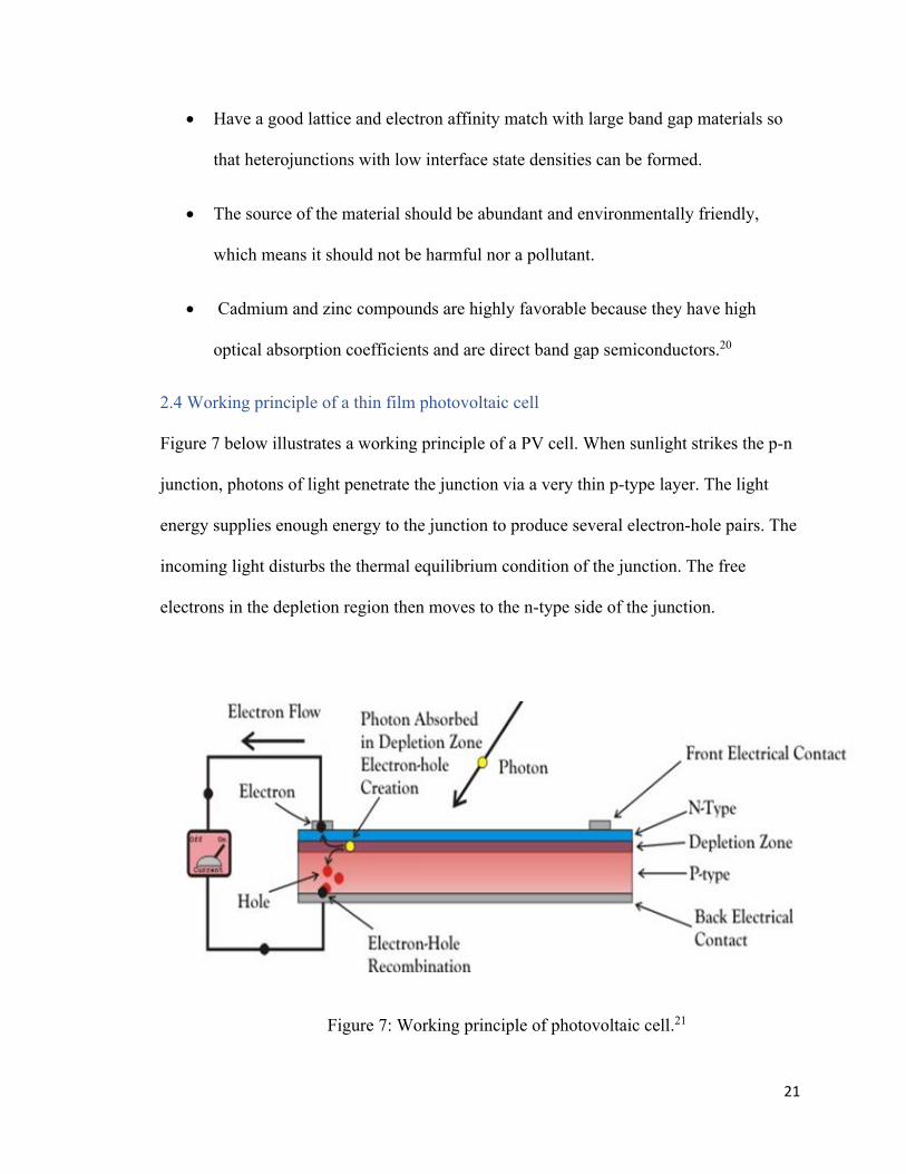
2.4 Working principle of a thin film photovoltaic cell
Figure 7 below illustrates a working principle of a PV cell. When sunlight strikes the p-n
junction, photons of light penetrate the junction via a very thin p-type layer. The light
energy supplies enough energy to the junction to produce several electron-hole pairs. The
incoming light disturbs the thermal equilibrium condition of the junction. The free
electrons in the depletion region then moves to the n-type side of the junction.
Figure 7: Working principle of photovoltaic cell.21

22
The holes in the depletion zone then quickly enter the p-type side of the junction. When
the newly created free electrons and holes enter the n-type side and p-type side
respectively, they cannot further cross the junction because of the junction’s barrier
potential.
When there is high concentration of electrons in the n-type side of the junction and the
hole concentration increases in the p-type side of the junction, then the junction behaves
like a small battery. A potential known as a photovoltage develops. If a small load is
connected across the p-n junction, a tiny current flows through it.21
2.5 The Shockley- Queisser Limit
It is also called the SQ limit. This is the highest theoretical efficiency of a PV cell using a
single p-n junction to draw power from the cell where the only loss mechanism is
radiative recombination in the PV cell. William Shockley and Hans-Joachim Queisser
first calculated it in 1961 and gave a maximum efficiency of 30% at 1.1 eV1. Follow up
calculations using global solar spectra (AM 1.5G) and including a back-surface mirror
have increased the efficiency to 33.7% for a cell with a band gap of 1.34 eV. This limit is
very key to energy production from the sun using PV cells and hence the most
fundamental concept in the field. Figure 8 below represents the recorded efficiencies of
materials in comparison to the SQ limit, their specific bandgaps, and the maximum
possible efficiency.22

23
Figure 8: A Shockley Queisser efficiency curve.22
When the sun irradiates on the PV cells, not all the incident sunlight gets absorbed. The
shortcircuit density, Jsc, is less than the maximum value achievable for a specific band
gap. The open circuit voltage, Voc of the cell is lowered by factors like bulk and interface
recombination and surface defects. Resistance and contact losses and other non-idealities
reduce the fill factor, which is as shown in Figure 2.5 below.
(a)

24
(b)
Figure 9: A I-V relationship of a solar cell.23
Figure 9 (a) implies that when no light is incident on the cell, a PV cell is equivalent to a
semiconductor current rectifier. The concentration of carriers in an illuminated cell is
more than those of the values with no illumination. In Figure 9 (b), the fill factor, which
is a measure of ideality in PV performance is given by the relationship shown below:
Where, Impp-maximum power current in A
Vmpp-maximum power voltage in V
Isc-short circuit current in A
Voc-open circuit voltage in V
The challenges faced by the solar cells lower their efficiencies relative to than the SQ
limit.23 Recent studies have proposed that implementing nanomaterials and
nanotechnology into the existing solar cells can result in improved efficiency and lowered
cost of the photovoltaic materials.24

25
2.6 Semiconductors and photoelectrochemistry
Semiconductors consist of valence and conduction bands. In the ground state, both holes
and electrons are in valence band while the conduction band is empty. When irradiated,
an electron in the valence band is promoted to the conduction band, while at the same
time making a hole remain in the valence band. Besides photochemical or thermal
excitation of electrons into the conduction band, doping can be used to generate holes and
electrons in semiconductors. Doping is the addition of a different element into the
semiconductor to improve its conductivity. Undoped semiconductors are also called
intrinsic semiconductors. Doped semiconductors which have electrons as the majority
charge carriers are called n-type semiconductors and those in which holes are the main
charge carriers are called p-type semiconductors.
The energy difference between the top of the valence band and bottom of the conduction
band is called band gap; it is also known as a gap because there are no electronic energy
levels in the interval. The wider the band gap, the harder it is to thermally excite electrons
from the valence to the conduction band. The relative position of a conduction band
versus valence band determines if a material is either a conductor, semiconductor, or an
insulator. For instance, a metal like copper has a band gap equal to 0 eV, hence a
conductor. A material like Si whose band gap is 1.1 eV is a semiconductor, while
insulators like TiO2 have a wider band gap of 3.0 eV.
Fermi energy, Ef, is the electronic energy level where the probability of finding an
electron in solid state materials is 50%. It is also defined as the highest occupied quantum
state at absolute zero temperature. The electron distribution among the energy levels is
determined by the Fermi-Dirac statistics equation shown below:
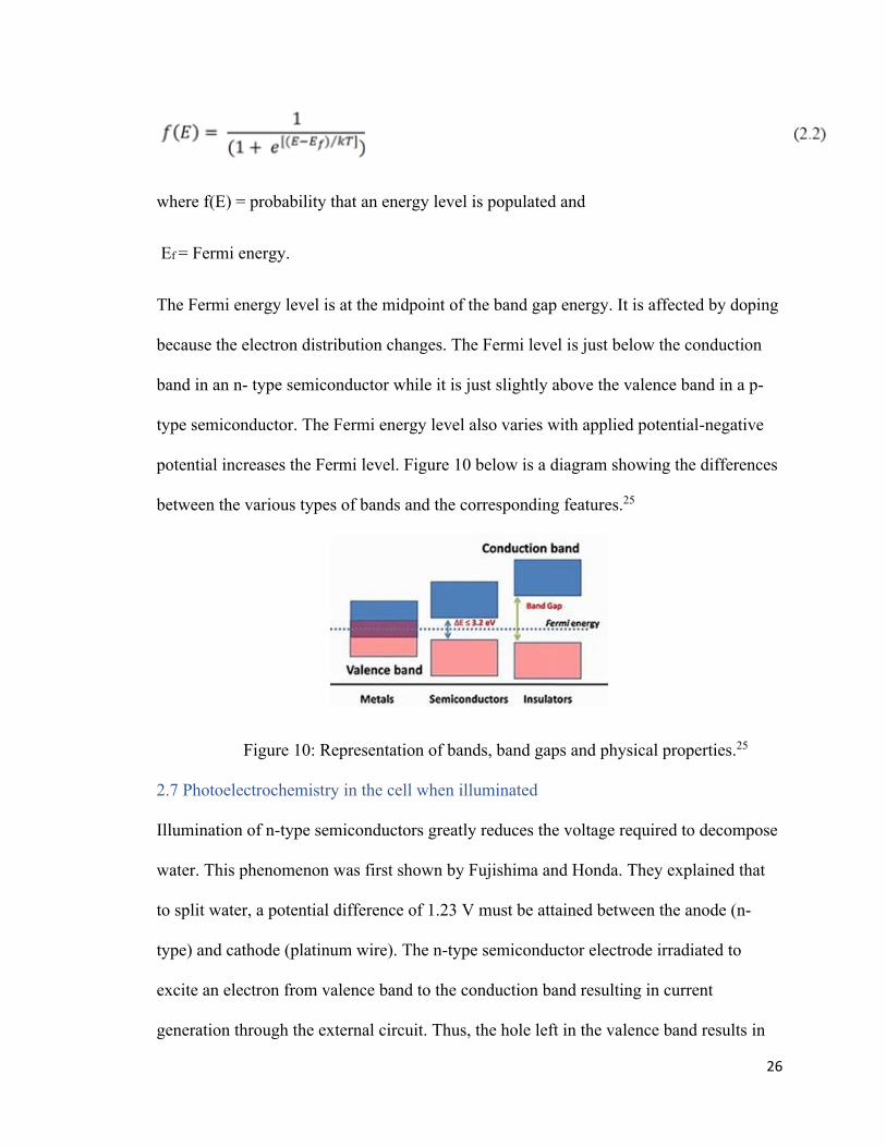
26
where f(E) = probability that an energy level is populated and
Ef = Fermi energy.
The Fermi energy level is at the midpoint of the band gap energy. It is affected by doping
because the electron distribution changes. The Fermi level is just below the conduction
band in an n- type semiconductor while it is just slightly above the valence band in a p-
type semiconductor. The Fermi energy level also varies with applied potential-negative
potential increases the Fermi level. Figure 10 below is a diagram showing the differences
between the various types of bands and the corresponding features.25
Figure 10: Representation of bands, band gaps and physical properties.25
2.7 Photoelectrochemistry in the cell when illuminated
Illumination of n-type semiconductors greatly reduces the voltage required to decompose
water. This phenomenon was first shown by Fujishima and Honda. They explained that
to split water, a potential difference of 1.23 V must be attained between the anode (n-
type) and cathode (platinum wire). The n-type semiconductor electrode irradiated to
excite an electron from valence band to the conduction band resulting in current
generation through the external circuit. Thus, the hole left in the valence band results in

27
water oxidation at the semiconductor while the electron obtained in the conduction band
will cause reduction of H+ ions at the Pt counter electrode as illustrated in the equations
below:
while the net equation is as follows:
2.8 Advantages and disadvantages of thin film solar cells
Thin film PV cells have both merits and demerits. The main advantages include:
• They are associated with minimal pollution.
• They are durable.
• No maintenance cost and possess minimum processing cost.
• Are made from inexpensive substrates like glass, polymers, or readily available
metals.
• Can be produced over a large area substrate producing a high output at cheaper
cost.
The following are some major disadvantages.
• It has high initial cost of installation.
• They can have low efficiency.

28
• When it is not sunny like on cloudy days, the energy produced cannot be relied
upon unless well stored.
• Reproducing of large area uniform films is not guaranteed.
• Polycrystalline materials have grain boundaries whose crystal defects act as
recombination centers.
2.9 Deposition techniques
The process of coating a thin layer on the surface of a substrate is known as thin-film
deposition. It also implies any method for depositing a thin coating of material onto a
substrate or on the surface of a previously deposited layer or layers. "Thin", in this
context, represents layer thickness to the tunes of nanometers to a few micrometers.
It is a useful technique used in the manufacture of optics, for reflective, anti-reflective
coatings among others; electronics such as layers of insulators, semiconductors, and
conductors for integrated circuits, and for packaging like aluminum-coated polyester
(PET) films.26 Deposition techniques are grouped into two major categories, depending
on whether the process is primarily chemical or physical as shown in Table 2.1 below.

29
Table 3: Thin film deposition methods.
Physical deposition Chemical deposition
1. Evaporation techniques
a) Vacuum thermal evaporation.
b) Electron beam evaporation.
c) Laser beam evaporation.
d) Arc evaporation.
e) Molecular beam epitaxy.
f) Ion plating evaporation.
2. Sputtering techniques
a) Direct current (DC) sputtering
b) Radio frequency (RF) sputtering.
1. Sol-gel technique
2. Spray pyrolysis technique
3. Plating
a) Electroplating technique.
b) Electroless/chemical bath deposition.
4. Chemical vapor deposition
a) Low pressure vapor deposition.
b) Plasma enhanced vapor deposition.
c) Atomic layer deposition.27
2.10 Statement of the problem
The energy from the sun is one of the most abundant and green sources of renewable
energy of our planet. Over the years PV cells have been developed to tap electricity from
the sun but their costs of production must be reduced. The electroless plating method is
proposed in this study to greatly lower their cost of production.
2.11 Significance of the study
The objective of this study is to reduce Cd2+, TeO32- and HTeO2+ ions using suitable
reducing agents and /or complexing agents onto a stainless steel 304 substrate to form a
CdTe thin film for photovoltaic application. Electroless deposition (ED) method is to be
used as a cheaper alternative in the production of thin films. The previous research of
30
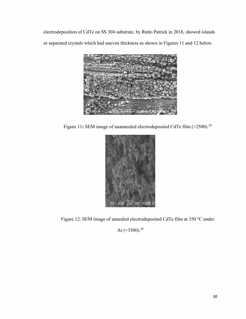
electrodeposition of CdTe on SS 304 substrate, by Rutto Patrick in 2018, showed islands
or separated crystals which had uneven thickness as shown in Figures 11 and 12 below.
Figure 11: SEM image of unannealed electrodeposited CdTe film (×2500).28
Figure 12: SEM image of annealed electrodeposited CdTe film at 350 oC under
Ar (×3500).28
31
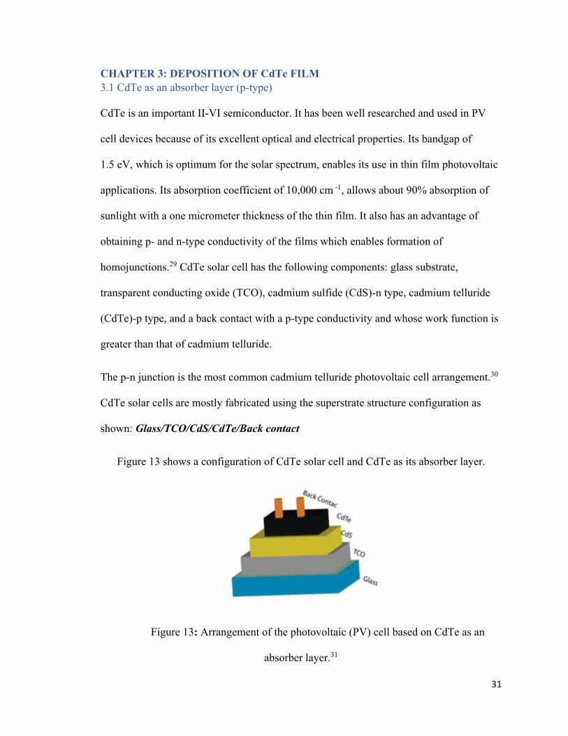
CHAPTER 3: DEPOSITION OF CdTe FILM 3.1 CdTe as an absorber layer (p-type)
CdTe is an important II-VI semiconductor. It has been well researched and used in PV
cell devices because of its excellent optical and electrical properties. Its bandgap of
1.5 eV, which is optimum for the solar spectrum, enables its use in thin film photovoltaic
applications. Its absorption coefficient of 10,000 cm -1, allows about 90% absorption of
sunlight with a one micrometer thickness of the thin film. It also has an advantage of
obtaining p- and n-type conductivity of the films which enables formation of
homojunctions.29 CdTe solar cell has the following components: glass substrate,
transparent conducting oxide (TCO), cadmium sulfide (CdS)-n type, cadmium telluride
(CdTe)-p type, and a back contact with a p-type conductivity and whose work function is
greater than that of cadmium telluride.
The p-n junction is the most common cadmium telluride photovoltaic cell arrangement.30
CdTe solar cells are mostly fabricated using the superstrate structure configuration as
shown: Glass/TCO/CdS/CdTe/Back contact
Figure 13 shows a configuration of CdTe solar cell and CdTe as its absorber layer.
Figure 13: Arrangement of the photovoltaic (PV) cell based on CdTe as an
absorber layer.31

32
The unit cell structure of cubic cadmium telluride is as shown in Figure 14 below.
Figure 14: Unit cell crystal structure of CdTe32.
Some properties of CdTe are as summarized in Table 3.1 below.
Table 4: Properties of CdTe.
Different Properties of Cadmium Telluride1
Chemical formula CdTe
Appearance Black solid
Formula weight 240 g/mole
Density 5.85 g/cm3
Melting point 1,314K
Boiling point 1,323K
Solubility in H2O Does not dissolve
Solubility in organic solvents Does not dissolve
Band gap 1.5 eV (@300 K, direct)
Refractive index (nD) 2.67 (@10 µm)
Conductivity p-type

33
3.2 Why CdTe?
Cadmium telluride solar panels have several advantages over traditional Si technology.
These advantages include:
• Easy to manufacture- electric fields, which makes solar energy conversion into
electricity possible, emanates from properties of CdS and CdTe molecules.
• Cd is an abundant element: it is obtained as a by-product of other industrial metals
like zinc and hence it does not experience wider price fluctuations as the case with
Si.
• High efficiency compared to Si.
• PV cells made from CdTe are cheaper.
• Forms a stable photo-electrode.
• Has 1.5 eV bandgap energy, which is closer to the maximum PV efficiency band
gap of 1.34 eV, according to the Schockley-Quiesser efficiency curve. This makes
it a good match with solar spectrum because its high absorption coefficient
enables it to absorb solar radiation at an ideal wavelength hence capturing energy
at shorter wavelengths.33
CdTe however, has drawbacks which limit its usage and hence, its application in solar
cells. This includes toxicity of Cd and that Te is an extremely rare earth element
estimated to occur at about 1-5 parts per billion in the Earth's crust.
3.3 The Pourbaix diagram of CdTe – H2O system
Potential-pH diagrams, also referred to as Pourbaix diagrams, are named after the
originator, Marcel Pourbaix (1963), a Belgian electrochemist and corrosion scientist. The

34
diagrams represent the stability of different forms of an element as a function of potential
and pH. Pourbaix diagrams are commonly used to assess the effects of pH, reduction-
oxidation potentials, and activities of potential-determining ions on the chemical
processes of rock and soil formation. An analysis of the Pourbaix diagram for the CdTe–
H2O system makes it possible to locate the pH and stability limits of CdTe. Chemical
etching of cadmium telluride is possible in strongly acidic (pH < 0.37) and strongly
alkaline (pH > 13.5) solutions. This diagram can be used to predict the state of the CdTe
surface as a function of solution pH and potential. CdTe is shown to have stability limits
at lines 1 and 4 (lower limit) and 5, 11 and 12 (upper limit). For instance, the table
indicate that uniform CdTe dissolution is only possible in strongly acidic solutions at
potentials above 0.4 V. This implies that, in these ranges of pH values and potentials,
uniform CdTe deposition is possible. Figure 15 below shows the Pourbaix diagram of the
CdTe–H2O system.34

35
Figure 15: Equilibrium potential–pH (Pourbaix) diagram of the CdTe–H2O
system.
3.4 Electroless deposition technique
Electroless deposition (ELD) is a method for preparing thin films of metals, their alloys,
and compounds. It is a relatively low temperature process-usually the chemical
temperature is less than the boiling point of the electrolyte. It is a cheap growth technique
which can produce good quality thin film semiconductors over large surface area unlike
other physical and chemical vapor deposition methods. ELD produces uniform films that
are of good quality under optimum growth conditions.
In this plating procedure, a chemical reducing agent like sodium hypophosphite,
hydrazine or formaldehyde is used to reduce metal ions. A coating is formed on the

36
substrate surface. It is called a solution growth technique or controlled precipitation and
is majorly used to prepare metal oxide and chalcogenide thin films.35 In this solution
growth technique, the precursor solution of metal ions must be complexed by ligands to
prevent the precipitation of insoluble intermediates. The complexation can be achieved
by adding ligands like ammonia (NH3) solution, triethanolamine (TEA), ethylene-
diamine-tetra acetic acid (EDTA), sodium citrate, among others.
The deposition process takes place in the absence of external electrical energy. It is an
autocatalytic process, where the coating material or alloy (in this case CdTe) catalyzes
the reaction to ensure that the coating process keeps going.
The electroless process is so called because it does not follow the electrodeposition
principle but instead is a chemical process, where metal layers are deposited by reducing
metal ions present in a hot aqueous solution. The substrate is first cleaned and then
immersed into the electrolyte which serves as the plating solution. Substrates are dipped
in any orientation inside the solution and left until they attain the desired film thickness.36
This procedure employs numerous simultaneous reactions in an aqueous solution that
must usually be subjected to heating. The coating process is a REDOX (reduction-
oxidation) reaction where both reduction (gaining of electrons) and oxidation (loss of
electrons) take place simultaneously. The expected equation for the reduction of HTeO2+
ion (oxidation state of tellurium is +4, Te4+) to an oxidation state of 0 (Te0) for the 1st
approach (described in Section 4.3) is as shown in equation 3.1 below.
The ELD procedure depends on several factors like pH of the electrolyte, stability of the
37
bath, temperature, deposition time, concentration of the electrolyte, purity of the reagents
and the type of the substrate in terms of its smoothness, crystallinity, and surface
treatment. Stainless steel 304 substrate was chosen in this project because of its resistance
to corrosion and its surface conductivity.37
3.4.1 Literature review on electroless deposition
There are a few reports in the literature on the ELD process for fabricating CdTe thin
films. Padam and Malhotra deposited CdTe on glass, ITO-coated glass, Si wafer and
mica using solutions of cadmium chloride and tellurium oxide in alkaline medium along
with triethanolamine (TEA) and hydrazine hydrate.38 Klochko et al. deposited
CdTe thin film in acidic medium using cadmium sulfate and tellurium oxide.39
Deivanayaki et al. used cadmium acetate and tellurium oxide to deposit CdTe thin films
under a nitrogen atmosphere but there is no mention of the pH of the solution.40
Garadkar et al. deposited CdTe thin films using sodium tellurosulphite as a source of
tellurium and cadmium sulfate as the source of cadmium.41 Most of the depositions have
been carried out at temperatures in the range of 50˚C - 100˚C. In this paper, some of the
deposition parameters are varied: two complexing and five reducing agents// are used,
time of deposition varied, and the results of the different forms of cadmium telluride thin
films obtained are presented.42
3.4.2 Why electroless deposition?
Among all the different deposition techniques, ELD is chosen because it:
• has no external electrical contact required hence no current distribution issues.
• can coat thin films of metals, alloys, and compounds on insulators like glass,
ceramics, and polymers.
38
• is a simple deposition tool in comparison to other metallization techniques.
• is a low temperature process compared to other vacuum procedures.
• is a relatively cheaper method compared to other physical and chemical vapor
deposition methods.43
• does not require a vacuum environment.
• produces uniform films that are of good quality under optimum growth
conditions.
3.4.3 Drawbacks of electroless deposition
Electroless deposition, however, has its own fair share of challenges because the
electrolytes contain a few components such as metal complex ions, reducing agents, pH
adjustment and buffering components or other additives, which can affect both the
process and the thin film quality.43 Some problems associated with ELD include:
• Aging of the solution,
• Byproducts can react – this affects the coating process.
• Nucleation on nontargeted regions and failure to nucleate or grow films on
selected regions due to contamination or some other problems associated with the
catalytic surface.
• The procedure is time-consuming.
3.4.4 Components of electroless deposition
Components that are required to carry out an electroless process include:
• A substrate where the deposition is going to take place.
• The bath-a solution that is made up of common reactive salts.

39
• A beaker for the solution bath.
• A water bath to ensure that temperature is uniformly distributed.35
• A device to regulate the stirring process and temperature.
Figure 16 below is a schematic diagram representing the ELD process.35
Figure 16: A schematic diagram representing the ELD process.35
3.4.5 Reducing agents and ligands.
ELD derives the driving force from a reducing agent and the auto-catalytic property of
the deposited metal. If a ligand is used as a complexing agent, it should be added in
excess in comparison to the stoichiometric reaction involved in the formation of the metal
complex. This is to ensure that the electroactive complex species are continuously
available throughout the coating process and to ensure that the rapid formation of the
electroactive complex from the Mn+ ions are brought into the solution by the reaction:
[M Mn+]. Table 3.2 below shows the properties of some reducing agents.

40
Table 5: Properties of some reducing agents
Reducing agent
Number of electrons involved Redox potential (vs. NHE) (V)
Aluminum 3 -1.66
Sodium hypophosphite
2 -1.40
Hydrazine 4 -1.16
Sodium borohydride
8 -1.20
Formaldehyde 4 -1.22
The above-mentioned reducing agents have the potential to reduce Te from Te4+(in
HTeO2+) to Te0 in the 1st approach (acidic) and to reduce Te from Te4+(in TeO32-) to Te0
in the 2nd approach (alkaline) considering that their redox potentials (vs. NHE) are more
than the reduction potentials, Eo red, of the reaction mechanisms as shown in equations
(3.2) and 3.3 below.
Cadmium ions (Cd2+) are also reduced from an oxidation state of +2 to 0 in the 2nd
approach as shown in equation (3.4) below:

41
The use of sodium hypophosphite and sodium borohydride reducing agents leads to
crystalline and amorphous deposits along with incorporation of elemental phosphorous
and boron, respectively. Hypophosphite as a reducing agent has a utilization efficiency of
about 35%. Hydrazine as a reducing agent produces coatings consisting of oxygen and
nitrogen with other trace elements. Hydrazine is a better reducing agent in alkaline media
than in acidic media. Some hydrazine is also oxidized to ammonia in the deposition
process. Studies confirm that chemical baths based on formaldehyde and hypophosphite
as reducing agents perform better in terms of stability and quality of the deposits.44
Figure 17 below represents an illustration of the electroless deposition technique.
Figure 17: An illustration of the electroless deposition technique.
42
CHAPTER 4: EXPERIMENTAL DETAILS
For the deposition experiments, bath temperature (Tb), was set at 70 oC and the deposition
was carried out between 5 and 30 minutes. The deposited CdTe films were then
characterized using scanning electron microscopy (SEM), X-ray diffraction (XRD),
profilometry, cyclic/linear voltammetry and energy dispersive spectroscopy (EDS). Our
main objective is to deposit a uniform CdTe film on SS 304 substrate using electroless
deposition method in an aim to form films of uniform thickness.
4.1 Substrate cleaning process
For this experiment, stainless steel 304 substrates (supplied by a local firm-Pilkington)
were used. After the substrates were selected, they were cut (using some pliers) into small
pieces about 3.0 cm by 1.0 cm, etched in concentrated HCl for 5 minutes, and then
prepared for the experiment by the “ultrasonic bath process”. The substrates were then
cleaned by a five-step procedure. In 1st step, the substrates were scrubbed with steel wool
for 2 minutes with ethanol and then rinsed with deionized water. This step was repeated 3
more times. In the 2nd step, the substrates were immersed in a beaker containing ethanol
and treated in an ultrasonic bath for 5 minutes. In 3rd step, the substrate was dipped in a
beaker containing acetone for 5 minutes. In the 4th step, the substrates were immersed in a
beaker containing ethanol again and then treated in an ultrasonic bath for 5 minutes. In
the 5th step, the substrates were dipped in a beaker containing deionized water and then
the beaker was treated in an ultrasonic bath for 10 minutes. Both acetone and ethanol
were used to remove oily and greasy impurities from the surfaces of the substrates by
dissolving them. Concentrated HCl was used to remove oxide layers from the surfaces of
the substrates while deionized water was used to rinse the substrates by washing the

43
impurities away.6 A ultrasonic bath instrument (BRANSON, MODEL B-42H) was used
in this experiment. Some cleaned and dried SS 304 substrates are shown in Figure 18
below.
Figure 18: Cleaned and dried out SS 304 substrates.
Figure 19: Electric tape attached at the rear side of the substrate.
The rear side of the substrates was covered with electric tape to ensure that CdTe coating
only happened on one side of the substrates as shown in Figure 19 above.
4.2 Chemical components Table 4.1 below shows the list of chemicals used in this study to deposit the CdTe films
on stainless steel substrate.

44
Table 6: List of chemicals/materials used.
Chemicals/materials Manufacturer Purity% Purpose of usage
Sodium hydroxide Fisher Scientific 99.5 Dissolving TeO2 Acetone VWR CHEMICALS 99.5 Cleaning
substrates Stainless steel 304 Pilkington Substrates Hydrochloric acid Fisher Scientific 35.5 Etching of the
substrates Sulfuric acid Pharmaco-AAPER 96.5 Dissolving of
TeO2, regulate pH
Ammonium hydroxide
Pharmaco-AAPER 29 Complexing agent, regulate pH
Tellurium (IV) oxide Alfa Aesar 99.99 Source of Te Cadmium acetate ACROS ORGANICS 98 Source of Cd Triethanolamine Fisher Scientific 99 Complexing
agent Hydrazine monohydrate
SIGMA- ALDRICH 64.5 Reducing agent
Sodium hypophosphite
ALDRICH 99 Reducing agent
Formaldehyde SIGMA 36.0 Reducing agent Sodium borohydride SIGMA- ALDRICH 98.5 Reducing agent Ethanol Pharmaco-AAPER 90.65 Cleaning
substrates Deionized water Prepare
solutions, rinse substrates
Electric tape Binder Aluminum rod Act as a reducing
agent ITO glass substrate Pilkington Substrate Cadmium telluride ALDRICH 99.99 Control/reference
4.3 Procedure
CdTe films were successfully deposited by using two approaches and five different
reducing agents:
45
• Approach I: using an Al rod as a reducing agent in an acidic medium.
• Approach II: using hydrazine hydrate, sodium hypophosphite, sodium
borohydride and formaldehyde as reducing agents in alkaline media.
In the two approaches, aqueous ammonia or TEA was used the complexing agent for the
slow release of Cd2+ as the cation, while the reducing agents were introduced to reduce
Te4+ to Te0 in the 1st approach and to reduce Te4+ to Te0 in 2nd approach as the anionic
precursors. Cd2+ was also reduced to Cd0 in both approaches. Stainless steel 304
substrates, approximately 3 by 1 cm were used. With the help of crocodile clips, all
substrates were kept vertically suspended in the solutions. Single dip deposition of each
sample was carried out.
In the 1st approach, 0.01 M cadmium acetate solution was prepared by dissolving 0.333
g of cadmium acetate dihydrate in distilled water. The solution was then topped off with
distilled water to make 125.0 cm3 of solution. A 0.01 M tellurium oxide solution was
prepared by dissolving 0.20 g of TeO2 in 1 M NaOH to make 125 cm3 of solution. The
two solutions were then mixed and stirred with a magnetic stirrer. A 10% H2SO4 solution
was then added dropwise to adjust the pH to 2. The mixture was then heated, and the
temperature of the mixture (bath) was adjusted to between 40 oC and 60 oC. The cleaned
and dried substrates were then immersed in the solution and suspended with copper
alligator clips such that the Cu was in contact with the solution. An Al rod was then
connected to the crocodile clip and short-circuited by being immersed into the solution.
The setup of the experiment is as shown in Figure 20 below.

46
Figure 20: Set up of the experiment conducted in the 1st approach.
The experiment was then left to run for between 5 and 30 minutes. The CdTe coatings
(black in color) were then annealed at 350 oC for 3 hours in a temperature-controlled
furnace, MODEL RTP-300 RAPID THERMAL PROCESSOR (made in China), in an
argon atmosphere.
In the 2nd approach, 0.5 M cadmium acetate was prepared by dissolving 13.327 g of
solid cadmium acetate in deionized water and then diluted with deionized water to make
100 cm3 of solution. In 20 ml of this solution, 5 ml of reducing agent (hydrazine
monohydrate or 36.5% formaldehyde solution or 1 M NaH2PO2 solution or 1 M NaBH4
solution) was added and 25% ammonia solution was then added dropwise until in excess,
(when a clear solution was obtained). The pH of the solution was then adjusted to 12.5 by

47
alternately adding NH3 (aq) and 10% H2SO4 dropwise. After adjustment of the pH of the
solution, the beaker was kept in a preheated water bath at 70 oC. The cleaned and dried
SS 304 substrates were then immersed in a vertical position in the beaker and the solution
was stirred with a magnetic stirrer. A 0.05 M solution of TeO32- was prepared by
dissolving 0.79799 g of TeO2 in 1 M NaOH to make 100 cm3 of solution. A 30 ml
portion of this solution was then added dropwise at a rate of 1 ml per minute in the
reaction mixture by using a burette fitted vertically as shown in Figure 21 below. The
colorless solution at the beginning of the experiment turns to dark grey color immediately
after immersion of Te ions evidencing the formation of cadmium telluride. After 30
minutes, the coated substrates were then detached, rinsed with distilled water to remove
loosely adhered particles, and naturally dried to get rid of excess moisture. After the
samples dried out, the electric tape attached at the rear side of the samples was removed
by carefully detaching it. The as-deposited films of cadmium telluride were annealed at a
temperature of 350 oC in a temperature-controlled furnace in an argon atmosphere for 3
hours.

48
Figure 21: Set up of the experiment conducted in the 2nd approach.
The same procedure was repeated with triethanolamine (TEA) as a complexing agent in
place of ammonia. This 2nd procedure was repeated three more times with sodium
hypophosphite, sodium borohydride and formaldehyde as the reducing agent. Figure 22
below shows the temperature-controlled furnace that was used in the annealing of our
samples.

49
Figure 22: A temperature-controlled furnace, (MODEL RTP-300 RAPID
THERMAL PROCESSOR).
4.4 Apparatus for determining surface morphology.
Scanning electron microscopy (SEM) was performed to provide detailed imaging
information about the morphology and surface texture of individual particles, as well as
elemental composition of samples. In our study, the samples were cut into approximately
3 mm × 3 mm pieces and mounted in the SEM-EDS chamber. A JEOL JIB-4500
apparatus pictured in Figure 23 below was used to carry out the SEM measurement. It is
a high-performance scanning electron microscope with an embedded energy dispersive
X-ray analyzer for EDS analysis.
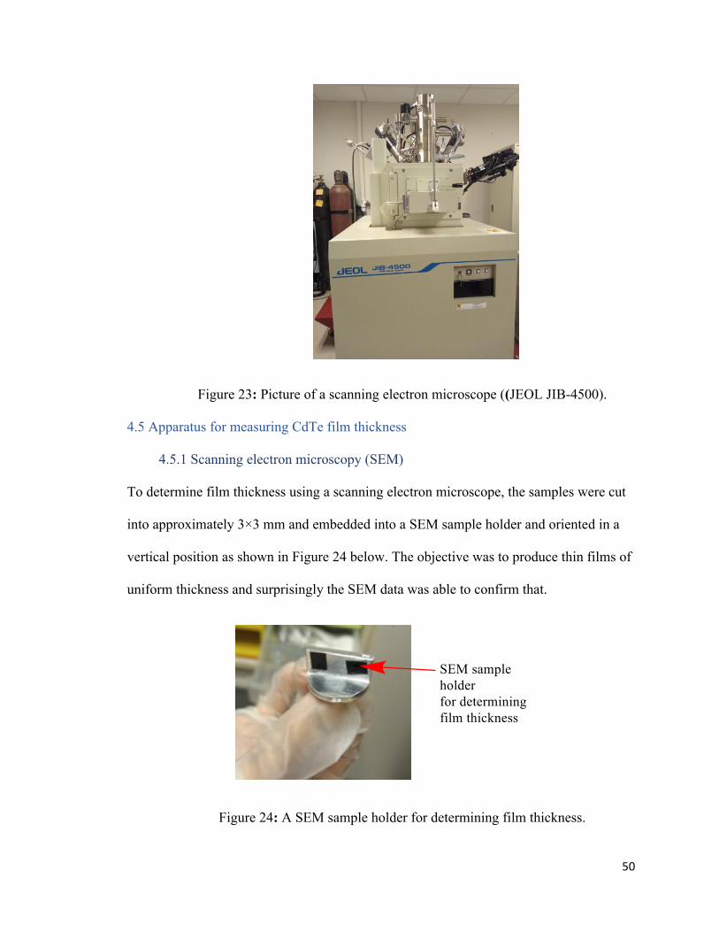
50
Figure 23: Picture of a scanning electron microscope ((JEOL JIB-4500).
4.5 Apparatus for measuring CdTe film thickness
4.5.1 Scanning electron microscopy (SEM)
To determine film thickness using a scanning electron microscope, the samples were cut
into approximately 3×3 mm and embedded into a SEM sample holder and oriented in a
vertical position as shown in Figure 24 below. The objective was to produce thin films of
uniform thickness and surprisingly the SEM data was able to confirm that.
Figure 24: A SEM sample holder for determining film thickness.
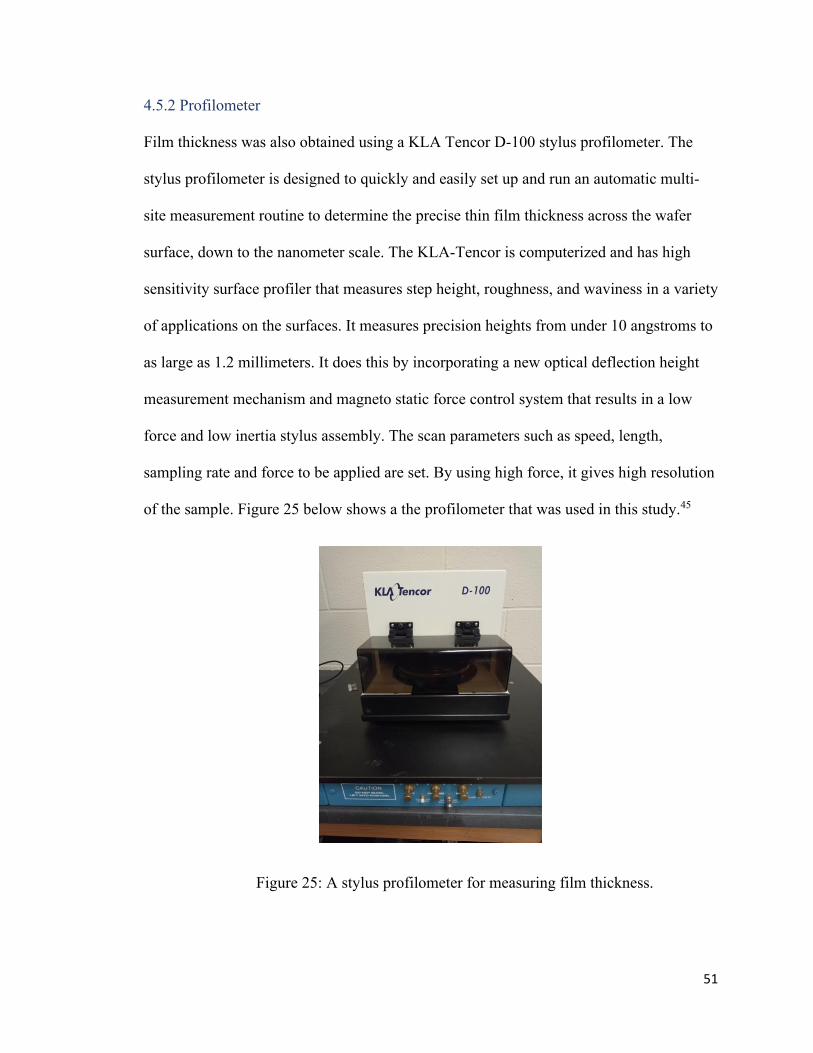
51
4.5.2 Profilometer
Film thickness was also obtained using a KLA Tencor D-100 stylus profilometer. The
stylus profilometer is designed to quickly and easily set up and run an automatic multi-
site measurement routine to determine the precise thin film thickness across the wafer
surface, down to the nanometer scale. The KLA-Tencor is computerized and has high
sensitivity surface profiler that measures step height, roughness, and waviness in a variety
of applications on the surfaces. It measures precision heights from under 10 angstroms to
as large as 1.2 millimeters. It does this by incorporating a new optical deflection height
measurement mechanism and magneto static force control system that results in a low
force and low inertia stylus assembly. The scan parameters such as speed, length,
sampling rate and force to be applied are set. By using high force, it gives high resolution
of the sample. Figure 25 below shows a the profilometer that was used in this study.45
Figure 25: A stylus profilometer for measuring film thickness.
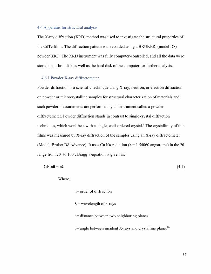
52
4.6 Apparatus for structural analysis
The X-ray diffraction (XRD) method was used to investigate the structural properties of
the CdTe films. The diffraction pattern was recorded using a BRUKER, (model D8)
powder XRD. The XRD instrument was fully computer-controlled, and all the data were
stored on a flash disk as well as the hard disk of the computer for further analysis.
4.6.1 Powder X-ray diffractometer
Powder diffraction is a scientific technique using X-ray, neutron, or electron diffraction
on powder or microcrystalline samples for structural characterization of materials and
such powder measurements are performed by an instrument called a powder
diffractometer. Powder diffraction stands in contrast to single crystal diffraction
techniques, which work best with a single, well-ordered crystal.1 The crystallinity of thin
films was measured by X-ray diffraction of the samples using an X-ray diffractometer
(Model: Bruker D8 Advance). It uses Cu Kα radiation (λ = 1.54060 angstroms) in the 2θ
range from 20o to 100o. Bragg’s equation is given as:
2dsinθ = nλ (4.1)
Where,
n= order of diffraction
λ = wavelength of x-rays
d= distance between two neighboring planes
θ= angle between incident X-rays and crystalline plane.46
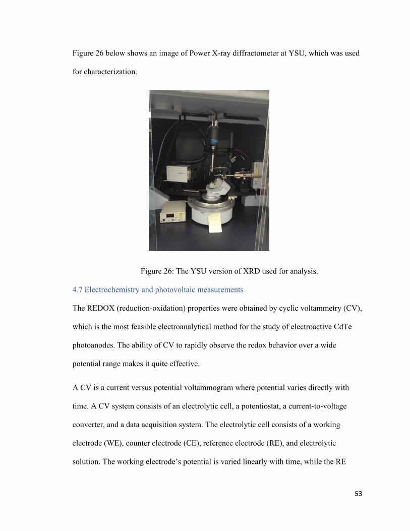
53
Figure 26 below shows an image of Power X-ray diffractometer at YSU, which was used
for characterization.
Figure 26: The YSU version of XRD used for analysis.
4.7 Electrochemistry and photovoltaic measurements
The REDOX (reduction-oxidation) properties were obtained by cyclic voltammetry (CV),
which is the most feasible electroanalytical method for the study of electroactive CdTe
photoanodes. The ability of CV to rapidly observe the redox behavior over a wide
potential range makes it quite effective.
A CV is a current versus potential voltammogram where potential varies directly with
time. A CV system consists of an electrolytic cell, a potentiostat, a current-to-voltage
converter, and a data acquisition system. The electrolytic cell consists of a working
electrode (WE), counter electrode (CE), reference electrode (RE), and electrolytic
solution. The working electrode’s potential is varied linearly with time, while the RE
54
maintains a constant potential. The CE conducts electricity from the signal source to the
WE. The purpose of the electrolytic solution is to provide ions to the electrodes during
oxidation and reduction. Photovoltage is measured by assembling the CdTe photoanodes
in the cell and then connected to a potentiostat and placed under a solar simulator, which
illuminates the photoelectrode.
A potentiostat is an electronic device which uses a direct current power source to
produce a potential, which can be controlled and accurately determined, while allowing
small currents to be drawn into the system without changing the voltage. The current-to-
voltage converter measures the resulting current, and the data acquisition system
produces the resulting cyclic voltammogram.47
4.7.1 Potentiostat
Voltametric experiments were performed using a 273 PAR potentiostat driven by
CorrWare. The electrode potential on the CdTe electrode was swept while current flow
was monitored. There was no current flow until oxidation and reduction at the electrode
occurred. When the potential develops over a set range in one direction, the direction is
reversed and swept back to the original voltage. This cycle can be repeated as many times
as desired.

55
CHAPTER 5: RESULTS AND DISCUSSION-CdTe Thin Film Characterization
5.1 Growth mechanism
In the electroless deposition technique, the uniform precipitation of water-insoluble
compounds and their solid solutions are controlled. This implies that for coating of thin
films of a compound such as CdTe, a solution of Cd2+ ions, with a complexing agent (or
ligand) L added to it, was prepared. The ligands which were used are NH3 and TEA. The
formation of the complex ions [Cd(L)i]2+ was the key factor in controlling the reaction.
This inhibited the immediate precipitation of the metal ions in the solution when the
precipitating anions were added to it. Since most of these processes were conducted in an
alkaline media, the CdTe film deposition was possible because the metal-ion
complexation prevented the precipitation of OH- ions.
The agent responsible for precipitation in the complex should be a compound which
gradually generates the anions in the solution upon hydrolysis. When the solution was
heated, the positive (Cd2+) ions were then generated after the complex species of
cadmium dissociated according to equation (5.1) below.
Film formation does not take place at room temperature since most of the Cd2+ ions are in
a bound complex state. The deposition temperature was kept above 60 oC to facilitate
film formation. The deposited CdTe films were annealed and then characterized using
scanning electron microscopy (SEM), X-ray diffraction (XRD), profilometry, cyclic
voltammetry and energy dispersive spectroscopy (EDS). The as-deposited films were
then annealed and analyzed.

56
5.2 Photographs of the CdTe thin films obtained.
The as-deposited CdTe films had a shiny finish when observed with the naked eye. The
color of the as-deposited films varied from dark ash color to brown which darkened after
annealing (as the case in Figure 28 below). They were opaque and uniformly adhered to
the substrate. The pictures of the uncoated SS and as-deposited films on SS 304
substrates are shown in Figures 27 to 32 below.
Figure 27: Image of stainless steel 304 substrate (uncoated sample).
Annealed (350 oC) As-deposited
Figure 28: Images of CdTe films coated on stainless steel prepared from
Approach I (Al as the reducing agent).
Annealed (350 oC) As-deposited
Figure 29: Images of CdTe films coated on stainless steel prepared from
Approach II (hydrazine hydrate as the reducing agent).
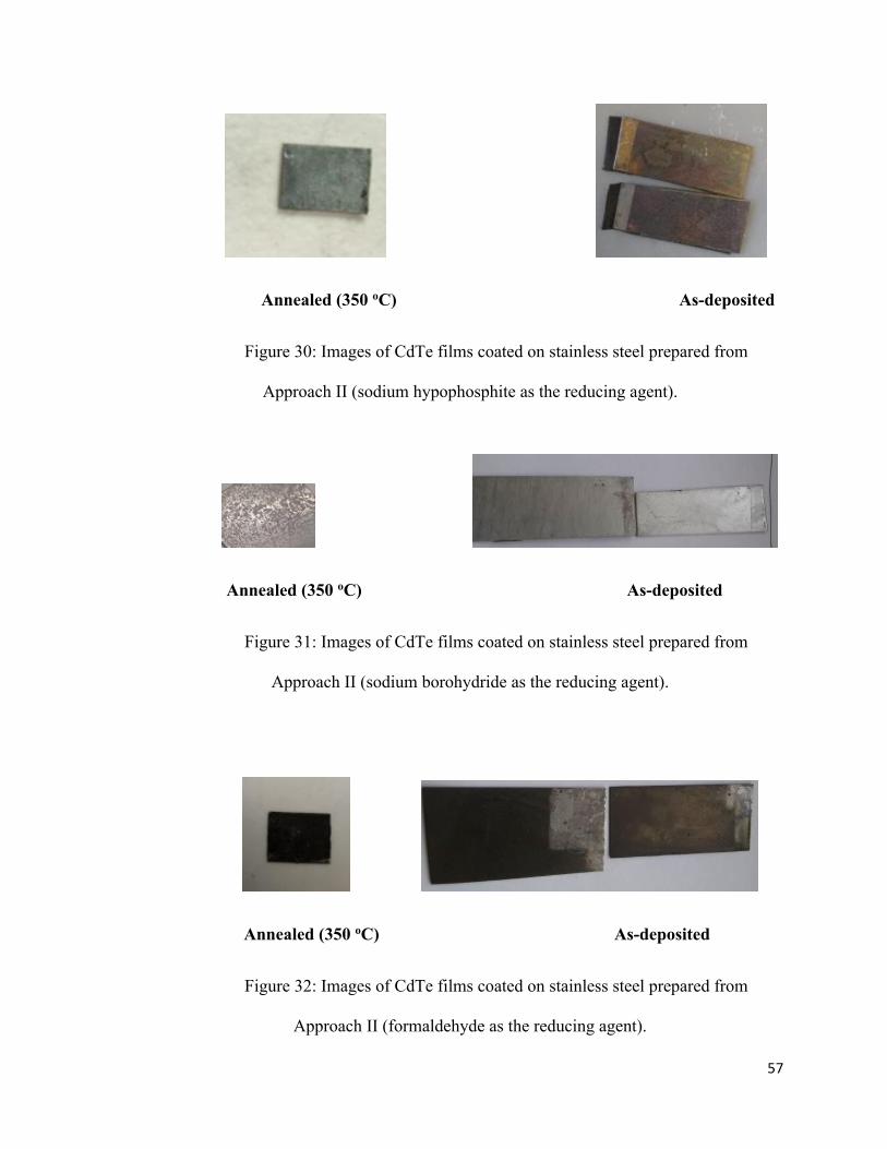
57
Annealed (350 oC) As-deposited
Figure 30: Images of CdTe films coated on stainless steel prepared from
Approach II (sodium hypophosphite as the reducing agent).
Annealed (350 oC) As-deposited
Figure 31: Images of CdTe films coated on stainless steel prepared from
Approach II (sodium borohydride as the reducing agent).
Annealed (350 oC) As-deposited
Figure 32: Images of CdTe films coated on stainless steel prepared from
Approach II (formaldehyde as the reducing agent).

58
5.3 Scanning electron microscopy (SEM)
Figures 33 to 38 below shows SEM micrographs (×1000) of deposited CdTe thin films. It
is observed that the films showed uniform distribution of agglomerated particles with
well-defined grain boundaries in some regions in the films prepared with Al as the
reducing agent. Samples prepared with NaBH4 as reducing agent have loose compact
particles with empty spaces between them. In the case of samples prepared with
hydrazine as the reducing agent, they are composed of minute crystals, implying loosely
connected particles and the corresponding data obtained from XRD indicates poor crystal
quality because of low temperature and rapid formation of CdTe from aqueous bath
methods. The as deposited and the annealed CdTe films are uniform and homogeneous
without pinholes or cracks in most of the obtained films, as well as covering the steel
substrate. It is observed that in the as-deposited films, the particles are compact and well
structured. Annealing the samples at 350 oC improved the crystallinity and the grain sizes
increased. The large changes in grain sizes in most of the samples can be attributed to
increased density, solvent loss, and crystallization.
Figure 33: SEM image of stainless Steel 304 (uncoated sample)

59
As-deposited Annealed (350 oC)
Figure 34: SEM images of as deposited and annealed (350 oC) CdTe films
prepared from Approach I (Al as the reducing agent).
As-deposited Annealed (350 oC)
Figure 35: SEM images of as deposited and annealed (350 oC) CdTe films
prepared from Approach II (hydrazine hydrate as the reducing agent).
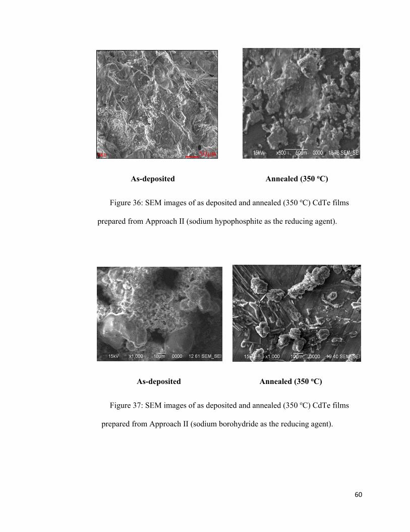
60
As-deposited Annealed (350 oC)
Figure 36: SEM images of as deposited and annealed (350 oC) CdTe films
prepared from Approach II (sodium hypophosphite as the reducing agent).
As-deposited Annealed (350 oC)
Figure 37: SEM images of as deposited and annealed (350 oC) CdTe films
prepared from Approach II (sodium borohydride as the reducing agent).

61
As-deposited Annealed (350 oC)
Figure 38: SEM images of as deposited and annealed (350 oC) CdTe films
prepared from Approach II (formaldehyde as the reducing agent).
5.4 SEM-EDS measurements for elemental composition
SEM–energy dispersive X-ray spectroscopy (EDS) technique was used to provide
detailed imaging information about the morphology and surface texture of individual
particles and elemental composition of the deposited coatings. The well-defined
boundaries indicate better bonding between Cd and Te. The films when ranked in order
of Cd: Te ratio shows that the films formed from aluminum, borohydride and
formaldehyde had about 1:1 while the Cd: Te ratio was about 1:2 in sodium
hypophosphite as the reducing agent. The ratio was the largest at about 1:15 in the case of
hydrazine reducing agent. Figures 39 to 44 below shows the EDS graphs of the deposited
films. The data indicates that considerable amounts of oxygen had been adsorbed on
CdTe surfaces even prior to treatment. This result agrees with other XPS studies
indicating that cadmium chalcogenides are likely to adsorb oxygen when exposed to
atmospheric oxygen.48 large changes in grain sizes in most of the samples can be
attributed to increased density, solvent loss, and crystallization.

62
Figure 39: SEM-EDS pattern of stainless steel 304 (uncoated sample).
Figure 40: SEM-EDS pattern of CdTe films coated on stainless steel prepared
from Approach I (Al as the reducing agent).

63
Figure 41: SEM-EDS pattern of CdTe films coated on stainless steel prepared
from Approach II (hydrazine hydrate as the reducing agent).
Figure 42: SEM-EDS pattern of CdTe films coated on stainless steel prepared
from Approach II (sodium hypophosphite as the reducing agent).

64
Figure 43: SEM-EDS pattern of CdTe films coated on stainless steel prepared
from Approach II (sodium borohydride as the reducing agent).
Figure 44: SEM-EDS pattern of CdTe films coated on stainless steel prepared
from Approach II (formaldehyde as the reducing agent).
5.5 Film thickness using a scanning electron microscopy (SEM)
The samples whose thickness was determined by SEM showed a thickness of about 66,
37 and 144 micrometers respectively as shown in the micrographs below. Figure 45 and
46 below shows uniform film thickness obtained from SEM micrographs.

65
Figure 45: SEM film thickness image of annealed (350 oC) CdTe films prepared
from Approach I (Al as the reducing agent).
Figure 46: SEM film thickness image of annealed (350 oC) CdTe films prepared
from Approach II (hydrazine hydrate as the reducing agent).
5.6 Film thickness using a stylus profilometer.
The data shown in Figures 47 to 51 below represents CdTe film thickness obtained from
the stylus profilometer for 5 samples. The film thickness was measured by a profilometer
and the results were about 24,6,10,12 and 10 microns for the films deposited,
respectively. When compared in terms of uniformity, the films obtained from sodium
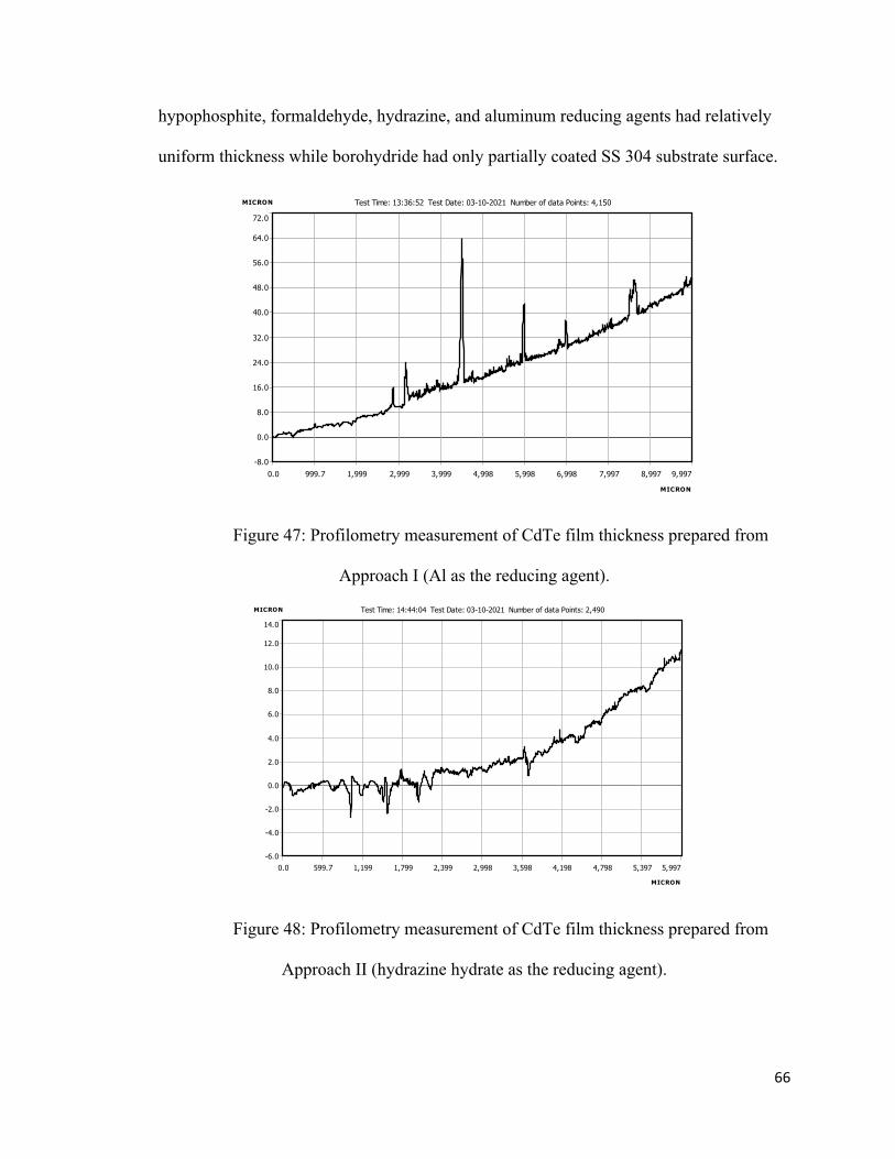
66
hypophosphite, formaldehyde, hydrazine, and aluminum reducing agents had relatively
uniform thickness while borohydride had only partially coated SS 304 substrate surface.
Figure 47: Profilometry measurement of CdTe film thickness prepared from
Approach I (Al as the reducing agent).
Figure 48: Profilometry measurement of CdTe film thickness prepared from
Approach II (hydrazine hydrate as the reducing agent).
-8.0
0.0
8.0
16.0
24.0
32.0
40.0
48.0
56.0
64.0
72.0
0.0 999.7 1,999 2,999 3,999 4,998 5,998 6,998 7,997 8,997 9,997
MICRON
MICRON Test Time: 13:36:52 Test Date: 03-10-2021 Number of data Points: 4,150
-6.0
-4.0
-2.0
0.0
2.0
4.0
6.0
8.0
10.0
12.0
14.0
0.0 599.7 1,199 1,799 2,399 2,998 3,598 4,198 4,798 5,397 5,997
MICRON
MICRON Test Time: 14:44:04 Test Date: 03-10-2021 Number of data Points: 2,490

67
Figure 49: Profilometry measurement of CdTe film thickness prepared from
Approach II (sodium hypophosphite as the reducing agent).
Figure 50: Profilometry measurement of CdTe film thickness prepared from
Approach II (sodium borohydride as the reducing agent).
-5.0
0.0
5.0
10.0
15.0
20.0
25.0
30.0
35.0
40.0
0.0 599.7 1,199 1,799 2,399 2,998 3,598 4,198 4,798 5,397 5,997
MICRON
MICRON Test Time: 14:34:32 Test Date: 03-10-2021 Number of data Points: 2,490
-4.0
0.0
4.0
8.0
12.0
16.0
20.0
24.0
28.0
32.0
36.0
0.0 599.7 1,199 1,799 2,399 2,998 3,598 4,198 4,798 5,397 5,997
MICRON
MICRON Test Time: 14:24:01 Test Date: 03-10-2021 Number of data Points: 2,490

68
Figure 51: Profilometry measurement of CdTe film thickness prepared from
Approach II (formaldehyde as the reducing agent).
5.7 X-Ray Diffraction (XRD) for structural analysis
The XRD patterns for the prepared samples are in Figures 52 to 65 below. The observed
broad rise in the XRD patterns at low angle is due to amorphous areas of the steel
substrate. Well-defined peaks were also observed. The peaks appearing on the left, at low
2θ degrees (between 20-30o) on the XRD patterns correspond to the cubic polycrystalline
structure of CdTe and is the major peak that strongly dominates the other peaks and was
found in samples produced from formaldehyde, hydrazine and sodium hypophosphite
reducing agents. The strong and sharp diffraction peaks in almost all samples indicated
that well crystallized samples were formed. Formaldehyde as a reducing agent produced
the best resolved XRD pattern in Figure 62 below. This XRD spectrum revealed that the
annealed CdTe films on SS 304 substrates are cubic crystalline in nature. The diffraction
peaks produced at 2θ = 23.754, 39.277, 46.419, 48.613 and 56.757 conform to the (111),
(220), (311), (222) and (400) hkl reflections associated with cubic crystal structure. From
-5.0
0.0
5.0
10.0
15.0
20.0
25.0
30.0
35.0
40.0
0.0 599.7 1,199 1,799 2,399 2,998 3,598 4,198 4,798 5,397 5,997
MICRON
MICRON Test Time: 14:34:32 Test Date: 03-10-2021 Number of data Points: 2,490

69
the X-ray diffractograms, it can be concluded that the deposited CdTe films were in the
cubic phase and hence the structure was reasonably crystalline. These results agree with
the XRD spectra obtained from a commercial CdTe powder and those reported in earlier
research.41 Annealing of the samples improved their crystallinity. The diffraction peaks
associated with SS 304 substrates occur at 2θ = 21o, 43o, 51o and 75o as shown in Figure
52 below. Since there is much oxygen on the CdTe surface, the peak at 2θ = 32o might be
related to elemental Cd or Te.
Figure 52: XRD pattern of uncoated stainless steel 304 substrates.
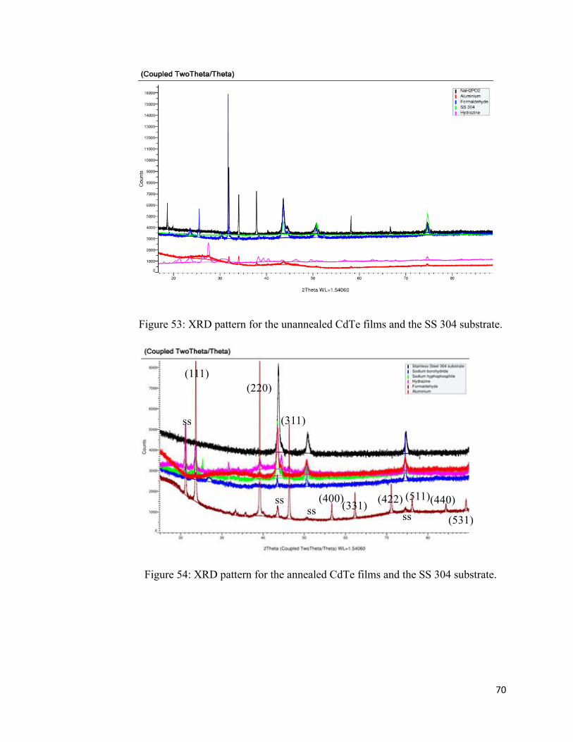
70
Figure 53: XRD pattern for the unannealed CdTe films and the SS 304 substrate.
Figure 54: XRD pattern for the annealed CdTe films and the SS 304 substrate.
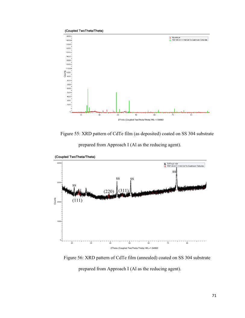
71
Figure 55: XRD pattern of CdTe film (as deposited) coated on SS 304 substrate
prepared from Approach I (Al as the reducing agent).
Figure 56: XRD pattern of CdTe film (annealed) coated on SS 304 substrate
prepared from Approach I (Al as the reducing agent).

72
Figure 57: XRD pattern of CdTe film (as deposited) coated on SS 304 substrate
prepared from Approach II (hydrazine as the reducing agent).
Figure 58: XRD pattern of CdTe film (annealed) coated on SS 304 substrate
prepared from Approach II (hydrazine as the reducing agent).
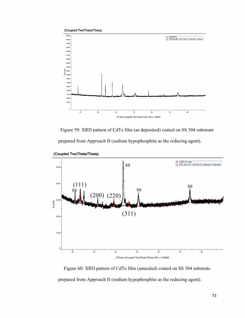
73
Figure 59: XRD pattern of CdTe film (as deposited) coated on SS 304 substrate
prepared from Approach II (sodium hypophosphite as the reducing agent).
Figure 60: XRD pattern of CdTe film (annealed) coated on SS 304 substrate
prepared from Approach II (sodium hypophosphite as the reducing agent).
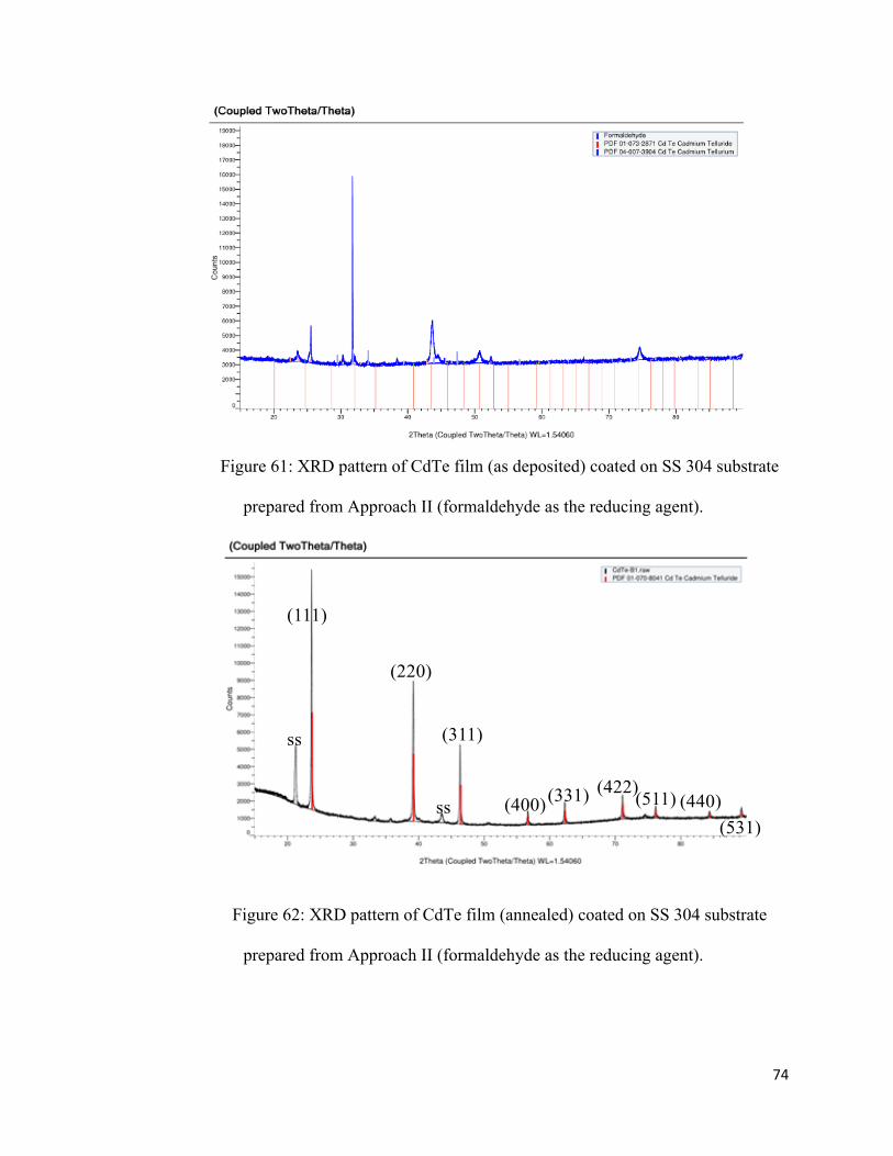
74
Figure 61: XRD pattern of CdTe film (as deposited) coated on SS 304 substrate
prepared from Approach II (formaldehyde as the reducing agent).
Figure 62: XRD pattern of CdTe film (annealed) coated on SS 304 substrate
prepared from Approach II (formaldehyde as the reducing agent).
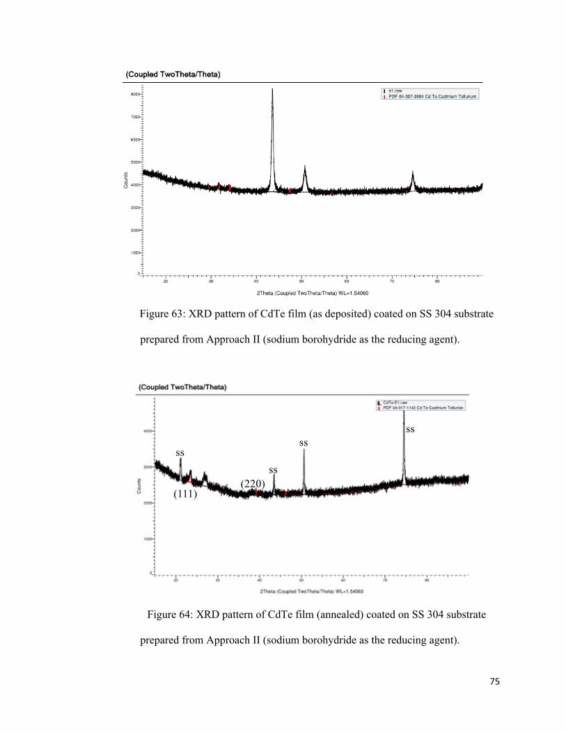
75
Figure 63: XRD pattern of CdTe film (as deposited) coated on SS 304 substrate
prepared from Approach II (sodium borohydride as the reducing agent).
Figure 64: XRD pattern of CdTe film (annealed) coated on SS 304 substrate
prepared from Approach II (sodium borohydride as the reducing agent).

76
Figure 65: XRD pattern of CdTe commercial powder.
5.8 Photoelectrochemical measurements/Cyclic voltammetry (CV)
Control cyclic voltammogram of SS 304 is shown below in Figures 66. There is evidence
of H2(g) evolution in both electrodes (reduction peaks) but there is a slight oxidation peak
in the case of the SS 304 substrate and none in the case of the Pt electrode. Figures 67
and 68 below shows the CV of CdTe under illumination and in darkness for unplatinized
sample and a platinized sample, respectively. It was noted that there was a slight increase
in the current by shining light on the SS 304 photovoltaic cell. Hydrogen evolution
increases when the CdTe electrode is used. A xenon lamp was used in this experiment as
the source of light to simulate sunlight. The effect of platinizing the deposited CdTe films
is that there was an increase in H2 gas evolution. This was made possible by sprinkling a
small amount of chloroplatinic acid into the electrolytic bath. Performing
photoelectrochemistry both in the light and dark did show some significant change in the
current. It was then concluded that platinizing activated the surface of the CdTe
electrode.

77
Key: Red-light ,black-dark
Figure 66: Cyclic voltammogram of SS 304-Control in the dark/light (1 M H2SO4,
Ag/AgCl reference electrode at 25 oC, scan rate 50 mV/s).
In the light In the dark
Figure 67: Cyclic voltammogram of CdTe/SS 304 in the light/dark (1 M H2SO4,
Ag/AgCl reference electrode at 25 oC, scan rate 50 mV/s, formaldehyde as the reducing
agent).

78
In the light In the dark
Figure 68: Cyclic voltammetry of Pt/CdTe/SS 304 in the light/dark (1 M H2SO4,
Ag/AgCl reference electrode at 25 oC, scan rate 50 mV/s, formaldehyde as the reducing
agent).
5.9 Photoelectrochemical measurements/Linear sweep voltammetry (LSV)
Linear sweep voltammetry is a voltammetric method where the current at a working
electrode is measured while the potential between the working electrode and a reference
electrode is swept linearly in time. Oxidation or reduction of species is registered as a
peak or trough in the current signal at the potential at which the species begins to be
oxidized or reduced.49 In terms of photoelectrochemical activity, the CdTe coated films
were ranked with their reducing agents from the one with the largest photocurrent to the
one with the lowest photocurrent as follows: Aluminum, sodium hypophosphite,
formaldehyde, sodium borohydride and hydrazine. The linear sweep voltammogram of a
blank SS 304 substrate is shown in Figure 69 below. In Figure 70, the instability might be
as a result Al doping of the CdTe films. There is an evidence of both reduction and
oxidation peaks in Figures 71 and 73 below. The oxidation peak (occurring above the
horizontal axis) represents the oxidation of the SS 304 substrate. Since the sweep is far
much negative, then it is H+ and not H2O that is being reduced-this occurs below the

79
horizontal axis. When H+ ions are reduced, then hydrogen gas is evolved which agrees
with the few bubbles formed. Figure 71 is an evidence that the CdTe film formed was p-
type since no hydrogen oxidation implied while Figure 73 represents an n-type of
semiconductor since hydrogen oxidation is observed.
Key: Red-dark, black-light
Figure 69: Linear sweep voltammetry of blank SS 304 in the dark/light (1 M
H2SO4, Ag/AgCl reference electrode at 25 oC, scan rate 5 mV/s, from -1.0 V to 0.0 V).
Key: Red-light ,black-dark
Figure 70: Linear sweep voltammetry of CdTe coated film in the dark/light (1 M
H2SO4, Ag/AgCl reference electrode at 25 oC, scan rate 5 mV/s, from -1.0 V to 0.0 V, Al
as the reducing agent).
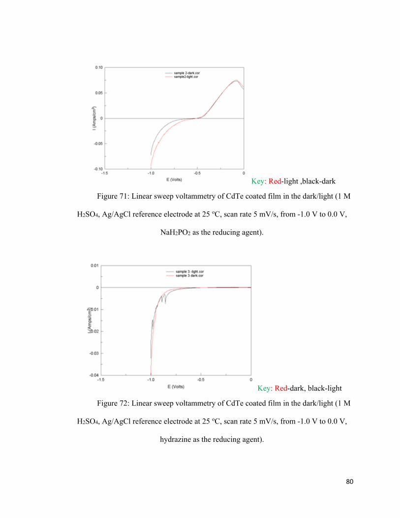
80
Key: Red-light ,black-dark
Figure 71: Linear sweep voltammetry of CdTe coated film in the dark/light (1 M
H2SO4, Ag/AgCl reference electrode at 25 oC, scan rate 5 mV/s, from -1.0 V to 0.0 V,
NaH2PO2 as the reducing agent).
Key: Red-dark, black-light
Figure 72: Linear sweep voltammetry of CdTe coated film in the dark/light (1 M
H2SO4, Ag/AgCl reference electrode at 25 oC, scan rate 5 mV/s, from -1.0 V to 0.0 V,
hydrazine as the reducing agent).
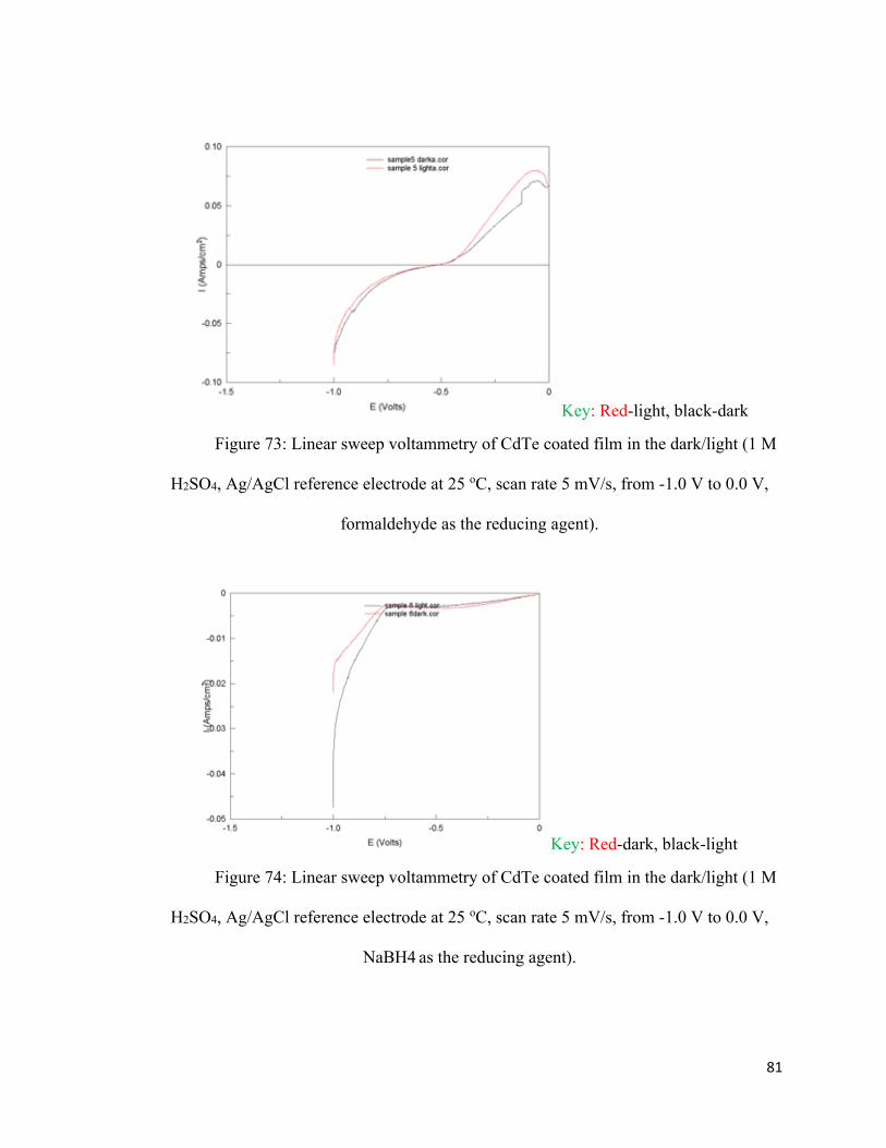
81
Key: Red-light, black-dark
Figure 73: Linear sweep voltammetry of CdTe coated film in the dark/light (1 M
H2SO4, Ag/AgCl reference electrode at 25 oC, scan rate 5 mV/s, from -1.0 V to 0.0 V,
formaldehyde as the reducing agent).
Key: Red-dark, black-light
Figure 74: Linear sweep voltammetry of CdTe coated film in the dark/light (1 M
H2SO4, Ag/AgCl reference electrode at 25 oC, scan rate 5 mV/s, from -1.0 V to 0.0 V,
NaBH4 as the reducing agent).
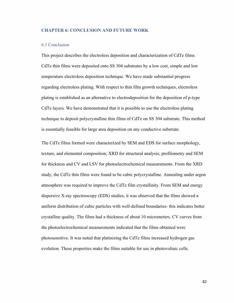
82
CHAPTER 6: CONCLUSION AND FUTURE WORK
6.1 Conclusion
This project describes the electroless deposition and characterization of CdTe films.
CdTe thin films were deposited onto SS 304 substrates by a low cost, simple and low
temperature electroless deposition technique. We have made substantial progress
regarding electroless plating. With respect to thin film growth techniques, electroless
plating is established as an alternative to electrodeposition for the deposition of p-type
CdTe layers. We have demonstrated that it is possible to use the electroless plating
technique to deposit polycrystalline thin films of CdTe on SS 304 substrate. This method
is essentially feasible for large area deposition on any conductive substrate.
The CdTe films formed were characterized by SEM and EDS for surface morphology,
texture, and elemental composition; XRD for structural analysis; profilometry and SEM
for thickness and CV and LSV for photoelectrochemical measurements. From the XRD
study, the CdTe thin films were found to be cubic polycrystalline. Annealing under argon
atmosphere was required to improve the CdTe film crystallinity. From SEM and energy
dispersive X-ray spectroscopy (EDS) studies, it was observed that the films showed a
uniform distribution of cubic particles with well-defined boundaries- this indicates better
crystalline quality. The films had a thickness of about 10 micrometers. CV curves from
the photoelectrochemical measurements indicated that the films obtained were
photosensitive. It was noted that platinizing the CdTe films increased hydrogen gas
evolution. These properties make the films suitable for use in photovoltaic cells.
83
6.2 Future work
We have not yet investigated the effects of photo-enhancement on the electrochemical
process, but we have gained an important step in understanding of the basic
electrochemistry of this material, and we have laid a steppingstone for photo-
enhancement research in the 2nd phase of this research. We propose that this work should
be pursued in the future. The following tasks are proposed as future work: - optimize the
procedures for the fabrication of CdTe and contact layers, including research on the effect
of grain size and grain boundary passivation, among others on photo-enhancement of the
ELD of CdTe, combine the mentioned approaches -into a single procedure for the
fabrication of the entire PV cell, and then publish results in the open literature.
Regarding device fabrication, we propose that the CdTe thin films prepared by ELD be
incorporated into the geometry: Glass/TCO/CdS/CdTe/Back contact with the SS 304 as
the substrate and Au as the back contact and we expect to demonstrate high efficiency
solar cells soon. Then we propose to develop a preliminary design of a large-scale
method suitable for CdTe module production.
84
REFERENCES
(1) https://www.wikipedia.com, the free encyclopedia; 2021.
(2) Bhand, S.; Salunke-Gawali, S. Amphiphilic Photosensitizers in Dye Sensitized
Solar Cells. Inorganica Chim. Acta 2019, 495, 118955.
https://doi.org/10.1016/j.ica.2019.118955.
(3) Solar Cell. Wikipedia; 2021.
(4) https://www.EnergyCite.
(5) Energy Is A Critical Enabler of Dignified and Fulfilled Lives. The Innovation
Village, 2020.
(6) Parvez, S.; Kamal, T. Chemical Bath Deposition of CdS Layer for CZTS Thin
Film Solar Cell. Bachelor's thesis, University of Dhaka, Bangladesh, July,2016.
(7) How long before we run out of fossil fuels? https://ourworldindata.org/how-long-
before-we-run-out-of-fossil-fuels (accessed Feb 17, 2021).
(8) Home - The Solar Energy Society of Canada Inc.
(9) Hemanth, D. J.; Kumar, V. D. A.; Malathi, S. Intelligent Systems and Computer
Technology; IOS Press, 2020.
(10) http://www.solar spectrum.png - (accessed Apr 22, 2021).
(11) Solar Energy. Wikipedia; 2021.
(12) Muradov, N.; Veziroglu, T. “Green” Path from Fossil-Based to Hydrogen
Economy: An Overview of Carbon-Neutral Technologies. Int. J. Hydrog. Energy
2008, 33 (23), 6804–6839. https://doi.org/10.1016/j.ijhydene.2008.08.054.
(13) Shahan, Z. Model 3 vs Bolt, Solar Cell Efficiency, Solar Energy Facts, Anti–Elon
Musk Lobbyists ... (Top 20 CleanTechnica Stories of the Week)
https://cleantechnica.com/2016/12/04/model-3-vs-bolt-solar-cell-efficiency-solar-
energy-facts-anti-elon-musk-lobbyists-top-20-cleantechnica-stories-week/
(accessed Feb 18, 2021).
(14) Dimova-Malinovska, D. The State-of-the-Art and Future Development of the
Photovoltaic Technologies - The Route from Crystalline to Nanostructured and
New Emerging Materials. J. Phys. Conf. Ser. 2010, 253, 012007.
https://doi.org/10.1088/1742-6596/253/1/012007.
85
(15) Green, M. A.; Emery, K.; Hishikawa, Y.; Warta, W.; Dunlop, E. Solar Cell
Efficiency Tables (Version 41); Progress in Photovoltaics. Res Appl 2013, 21:p 1-
11
(16) Figure 1.3 Different generations of solar cells
https://www.researchgate.net/figure/Different-generations-of-solar-cells-
4_fig1_317142351 (accessed Feb 18, 2021).
(17) Parvez, S.; Khabir, K.; Matin, R.; Hossain, T.; Sarwar, H.; Bashar, M.; Rashid, M.;
Mouri, T. K. Chemical Bath Deposition of CdS Layer for Thin Film Solar Cell.
SOUTH ASIAN J. Res. Eng. Sci. Technol. SAJREST 2017, 2, 610–617.
(18) Polman, A.; Knight, M.; Garnett, E. C.; Ehrler, B.; Sinke, W. C. Photovoltaic
Materials: Present Efficiencies and Future Challenges. Science 2016, 352 (6283).
https://doi.org/10.1126/science.aad4424.
(19) Cadmium Telluride https://www.energy.gov/eere/solar/cadmium-telluride
(accessed Feb 19, 2021).
(20) Research and development of CuInSe[2] based photovoltaic solar cells
https://1library.net/document/zwv4580q-research-development-cuinse-based-
photovoltaic-solar-cells.html (accessed Apr 12, 2021).
(21) Electrical4U. Electrical4U: Learn Electrical & Electronics Engineering (For Free)
https://www.electrical4u.com/ (accessed Apr 12, 2021).
(22) Rephaeli, E.; Fan, S. Absorber and Emitter for Solar Thermo-Photovoltaic Systems
to Achieve Efficiency Exceeding the Shockley-Queisser Limit. Opt. Express 2009,
17 (17), 15145. https://doi.org/10.1364/OE.17.015145.
(23) HASSAN ALI, M.; Rabhi, A.; El hajjaji, A.; Tina, G. Real Time Fault Detection in
Photovoltaic Systems. Energy Procedia 2016, p 11-13.
https://doi.org/10.1016/j.egypro.2017.03.254.
(24) Shockley, W.; Queisser, H. J. "Detailed Balance Limit of Efficiency of p-n
Junction Solar Cells" , Journal of Applied Physics, Volume 32, 1961, p 510-519 .
(25) Neamen, D. A. Semiconductor Physics and Devices: Basic Principles, 3rd ed.;
McGraw-Hill: Boston, 2003.
(26) Lin, B. Power and Energy Transduction In Piezoelectric Wafer Active Sensors For
Structural Health Monitoring: Modeling and Applications. Theses Diss. 2010.
86
(27) Alca Technology - Impianti e Componenti per l‘Industria e la Scienza
https://www.alcatechnology.com (accessed Apr 17, 2021).
(28) Rutto, P. ELECTRODEPOSITION OF CdTe ON STAINLESS STEEL 304
SUBSTRATES. Master’s thesis Youngstown State University, May 2018.
(29) Arce-Plaza, A.; Sánchez-Rodriguez, F.; Courel-Piedrahita, M.; Galán, O. V.;
Hernandez-Calderon, V.; Ramirez-Velasco, S.; López, M. O. CdTe Thin Films:
Deposition Techniques and Applications. Coat. Thin-Film Technol. 2018.
https://doi.org/10.5772/intechopen.79578.
(30) https://www.IntechOpen - Open Science Open Minds / (accessed Apr 17, 2021).
(31) Chander, S.; Dhaka, M. S. Enhancement in Microstructural and Optoelectrical
Properties of Thermally Evaporated CdTe Films for Solar Cells. Results Phys.
2018, 8, 1131–1135. https://doi.org/10.1016/j.rinp.2018.01.055.
(32) Anwar, F. Simulation and Performance Study of Nanowire CdS/CdTe Solar Cell,
Bachelor's thesis, University of Dhaka, Bangladesh, July,2016.
https://doi.org/10.13140/RG.2.2.25657.98400.
(33) Cadmium Telluride: Advantages & Disadvantages https://www.solar-facts-and-
advice.com/cadmium-telluride.html (accessed Feb 21, 2021).
(34) Voloshchuk, A. G.; Tsipishchuk, N. I. Equilibrium Potential–PH Diagram of the
CdTe–H2O System. Inorg. Mater. 2002, 38 (11), 1114–1116.
https://doi.org/10.1023/A:1020958330982.
(35) Mane, R.S.; Lokhande C.D. Chemical Deposition Method for Metal Chalcogenide
Thin Films. Mater. Chem. Phys.2000, p 1-31 .
(36) Jilani, A.; Abdel-wahab, M. S.; Hammad, A. H. Advance Deposition Techniques
for Thin Film and Coating. In Modern Technologies for Creating the Thin-film
Systems and Coatings; Nikitenkov, N. N., Ed.; InTech, 2017.
https://doi.org/10.5772/65702.
(37) Lahiri, A.; Pulletikurthi, G.; Endres, F. A Review on the Electroless Deposition of
Functional Materials in Ionic Liquids for Batteries and Catalysis. Front. Chem.
2019, 7. https://doi.org/10.3389/fchem.2019.00085.

87
(38) Padam, G. K.; Malhotra, G. L. Preparation and Study of CdTe Thin Films Grown
by the Solution Method. Mater. Res. Bull. 1989, 24 (5), 595–601.
https://doi.org/10.1016/0025-5408(89)90107-4.
(39) Klochko, N. P.; Volkova, N. D.; Kharchenko, M. M.; Kopach, V. R. "Contact
Electrodeposition of CdTe Thin Films", Functional materials, Vol. 16, 2009,
p.190-191.
(40) Deivanayaki, S.; Jayamurugan, P.; Mariappan, R.; Ponnuswamy, V. Optical and
Structural Characterization of CdTe Thin Films by Chemical Bath Deposition
Technique, Chacogenide Letters Vol. 7, No.3 2010, p. 159-163.
(41) Garadkar, K. M.; Pawar, S. J.; Hankare, P. P.; Patil, A. A. Effect of Annealing on
Chemically Deposited Polycrystalline CdTe Thin Films. J. Alloys Compd. 2010,
491 (1), 77–80. https://doi.org/10.1016/j.jallcom.2009.10.146.
(42) Gouda, L.; Aniruddha, Y. R.; Ramasesha, S. K. Correlation between the Solution
Chemistry to Observed Properties of CdTe Thin Films Prepared by CBD Method.
J. Mod. Phys. 2012, 03 (12), 1870. https://doi.org/10.4236/jmp.2012.312235.
(43) Shacham-Diamand, Y.; Osaka, T.; Okinaka, Y.; Sugiyama, A.; Dubin, V. 30years
of Electroless Plating for Semiconductor and Polymer Micro-Systems.
Microelectron. Eng. 2015, 132, 35–45. https://doi.org/10.1016/j.mee.2014.09.003.
(44) Rao, C. R. K.; Trivedi, D. C; Chemical and electrochemical depositions of
platinum group metals and their applications, Coordination Chemistry Reviews 249
(2005), p. 613-631
(45) Home https://www.epfl.ch/en/ (accessed Apr 17, 2021).
(46) Delsol, T. Research and Development of CuInSe2-Based Photovoltaic Solar Cells,
2001. Sheffield Hallam University, http://shura.shu.ac.uk/19551/
(47) Cyclic Voltammetry
https://chem.libretexts.org/Bookshelves/Analytical_Chemistry/Supplemental_Mod
ules_(Analytical_Chemistry)/Instrumental_Analysis/Cyclic_Voltammetry
(accessed Apr 5, 2021).

88
(48) Katari, J. E. B.; Colvin, V. L.; Alivisatos, A. P. X-Ray Photoelectron Spectroscopy
of CdSe Nanocrystals with Applications to Studies of the Nanocrystal Surface. J.
Phys. Chem. 1994, 98 (15), 4109–4117. https://doi.org/10.1021/j100066a034.
(49) Principles of Instrumental Analysis 5th Edition Pdf Free Download –
Stuvera.Com.