Error analysis of analytic solutions for self-excited near ...

Excited state dynamics of nanocrystalline VO2 with white lightcontinuum time resolved spectroscopy
Ulaş Kürüma, H. Gul Yaglioglu a,n, Betül Küçüköz a, R. Mustafa Oksuzoglu b,Mustafa Yıldırımb, A. Murat Yağcı b, Sami Pekdemir b, Ayhan Elmali a
a Department of Engineering Physics, Faculty of Engineering, Ankara University, 06100 Ankara, Turkeyb Department of Materials Science and Engineering, Faculty of Engineering, Anadolu University, 26470 Eskişehir, Turkey
a r t i c l e i n f o
Article history:Received 1 November 2013Received in revised form22 July 2014Accepted 23 July 2014Available online 7 August 2014
Keywords:Vanadium oxideUltrafast dynamicsPhase transitionWhite light continuum probe
a b s t r a c t
In an attempt to use ultrafast pump probe spectroscopy technique with white light continuum to revealwavelength dependent dynamics of VO2, bandgap needs to be opened. Therefore, nanostructuredamorphous and crystalline VO2 thin films were prepared with pulsed DC magnetron reactive sputtering.The mean diameters of grains were measured as 2270.1 nm and 4470.1 nm for amorphous andcrystalline VO2 thin films, respectively. Temperature dependent resistance measurements show thatnanocrystalline VO2 thin film exhibit metal insulator phase transition. The films exhibited dual bandgaps (2.3 eV, o0.6 eV for amorphous films and 1.3 eV, 1.8 eV for crystalline film). Increased band gapsmade it possible to perform time resolved transmission and reflection experiments with white lightcontinuum at fluences above and below photo induced phase transition threshold. Although transmis-sion chance due to photo induced phase transition of VO2 in the literature usually takes places at infraredregion of the spectrum, transmission chance was observed in visible as low as 630 nm in broadbandprobe spectra. It was observed that measured time scales depend on not only pump fluence but alsoprobe wavelength. Experiments gave the evidence of the long-lived lower energy non-equilibrium staterelated to the photo induced phase.
& 2014 Elsevier B.V. All rights reserved.
1. Introduction
Vanadium dioxide (VO2) is one of the technologically signifi-cant materials due to its ultrafast insulator to metal phase transi-tion (MIT) property. VO2 is an insulator semiconductor at roomtemperature. First order insulator to metal phase transition can beinduced either thermally, at 68 1C critical temperature or by laserexcitation [1–5]. Ultrafast light induced phase transition propertymakes VO2 films good candidates for optical applications such asactuators, optical switches, thermochromic windows, and diffrac-tive elements [6–11].
Although MIT of VO2 was discovered long ago [1], recentprogress in ultrafast time resolved techniques attracted attentionon light induced phase transition phenomena. Phase transitiondynamics of VO2 were investigated with time resolved optical [3],terahertz [12], X-ray spectroscopic [13], and crystallographic [4,5]measurements. These measurements revealed that due to ultrafastphotoexcitation of monoclinic VO2 insulator, ultrafast transition
takes place in not only atomic structural arrangement but alsoin electronic properties. These experiments were not able to concludewhether changing the symmetry of unit cell or creating instantaneousholes cause MIT. Time resolved spectroscopy experiment [14] with15 fs resolution revealed that MIT cannot be explained by onlyconsidering excitation of carriers across the semiconducting bandgap. Photo injection of holes into the valance band of insulator VO2
triggers nonthermal rearrangement in atomic and electronic struc-tures. Therefore, MIT can be explained by structurally mediatedtransition where transitional phonons connect the two crystallo-graphic phases [15]. On the other hand, recent study on ultrafast timeresolved THz spectroscopy of nanogranular VO2 revealed that both thetransition phonons and electronic excitations are necessary to drivethe ultrafast phase change throughout the film [16].
Ultrafast time resolved broadband spectroscopy is a powerfultool to investigate the nature of the dynamics in complex materi-als [17–19] and to study the photoinduced phase transitiondynamics [20] by fitting the broadband change in reflectivity datato the time dependent parametization of static dielectric function[21]. Since there are several broad spectral features overlappingfor VO2, it is difficult to analyze data to obtain whole dielectricfunction of the material [22]. However, qualitative assessment of
Contents lists available at ScienceDirect
journal homepage: www.elsevier.com/locate/optcom
Optics Communications
http://dx.doi.org/10.1016/j.optcom.2014.07.0640030-4018/& 2014 Elsevier B.V. All rights reserved.
n Corresponding author. Tel.: þ90 312 2033507; fax: þ90 312 2127343.E-mail address: [email protected] (H.G. Yaglioglu).
Optics Communications 333 (2014) 109–114

the data still gives valuable information about photoinduced phasetransition. If the optical band gap of VO2 is opened, ultrafast pumpprobe spectroscopy with white light continuum would revealwavelength dependent dynamics within the band gap of VO2. Itis known that the response of VO2 as well as the band gap can betailored by forming nanocrystals. For example, a new cubic crystalstructure for VO2 nanorods with a large optical band gap (2.7 eV)has been reported recently [23]. In another recent study, opticalproperties of nanostructured VOx thin films were altered bypost annealing in oxygen [24]. They have observed altered bandgap due to occupied states resulting from vanadium oxide withlow oxygen content. Therefore, we prepared nanostructured VO2
films followed by post annealing and investigated the ultrafastdynamics with pump probe spectroscopy experiment with whitelight continuum. We discuss here the experimental observation oftime resolved dynamics of nanocrystalline VO2 in a broad spectralrange within the white light continuum spectra.
2. Experiment
Thin film samples were deposited using the pulsed DC reactiveunbalanced magnetron sputtering technique. The deposition ratewas calibrated using the X-ray reflectivity technique and thethickness of the film was adjusted by the deposition time. Thefilm with 150 nm thickness was deposited onto 30�30 mm2
quartz substrate with an Ar:O2 gas flow ratio of 2:0.6 at 5 mTorrconstant deposition pressure, without substrate heating. Details ofthe pulsed DC reactive process are given elsewhere [25]. Post-annealing was performed at 400 1C (measured on the substratesurface) for 1 h under vacuum. Structures of investigated sampleswere determined by the Grazing incidence X-ray diffraction(GIXD) technique (GIXD, Bruker D8 Advance). The surface mor-phology and grain size were characterized using the AtomicForce Microscopy (VeecoMultimod 5-AFM with the analyze soft-ware Nanoscope 5). Temperature dependent resistance measure-ments were performed on annealed and as deposited filmsbetween 20 1C and 110 1C. The absorption spectra of the VO2 films(Fig. 4a) were taken using a UV–visible absorption spectrophoto-meter (Shimadzu UV-1800) versus an uncoated glass substrate asreference.
Wavelength dependent pump probe measurements were per-formed by using Ti:Sapphire laser amplifier-optical parametricamplifier system (Spectra Physics, Spitfire Pro XP, TOPAS) with44 fs pulse duration and 1 kHz repetition rate. Commercial pumpprobe experimental setup with white light continuum probe beam(Spectra Physics, Helios) was used. The pump wavelength was
chosen as 400 nm. Pulse duration inside pump probe experimen-tal set up was measured as 100 fs via cross correlation of pumpand probe pulses. Although the response of reflection and trans-mission pump probe experiments are connected, transmissionmode may show wavelength dependent excited state absorptionfeatures more clearly. Therefore, pump probe measurementswere performed in reflection and in transmission modes wherereflected and transmitted probe beams were monitored with fiberoptic spectrometer, respectively. According to our sign conventionpositive sign of pump probe data (ΔR/R) corresponds to decreasein reflection whereas negative sign corresponds to increase inreflection due to the effect of the pump beam in the reflectionmode. In transmission mode, positive sign of pump probe data(ΔT/T) corresponds to nonlinear absorption (NA) whereas negativesign of ΔT/T corresponds to saturable absorption (SA).
3. Results and discussion
GIXD patterns of as-deposited and annealed film indicate thatas deposited films have amorphous structure and annealed filmsshow VO2 crystal structure. Fig. 1a and b shows representativeAFM images of as deposited and annealed film, respectively. Fig. 1areveals that as deposited film has randomly distributed isolatedparticles with the grain size distribution varying from 1070.1 to3070.3 nm (mean diameter of grains is 2270.1 nm). As shown inFig. 1b, the post annealing induces an increment in the meandiameter of the grains and the distribution ranges from 1070.1 to7070.3 nm (mean diameter of grains is 4470.1 nm). As a resultof the structural analyses one can say that post annealing undervacuum not only increases the mean diameter of the nano-grainsand their distribution of nanostructured VO2 amorphous film, butalso causes nanocrystalline VO2 film to be formed.
It is known that the thickness of the film, presence ofimpurities and defects on the crystal structure as well as theparticle size play important role on the transition temperature.Therefore, MIT transition temperature gives information about thecharacteristics of the sample. Recently, transition temperature ofVO2 film was measured as 64 1C [26]. It was reduced significantlywith W doping. Transition temperature of V1�xWxO2 film (for x¼2.5) was measured about 32 1C. It is known that MIT temperatureof pure VO2 is 68 1C. Temperature dependent resistance measure-ments performed on as deposited films did not show any MITphase transition. However, annealed sample exhibit MIT (Fig. 2) atabout 62 1C on heating. Although transition temperature measure-ment of nanocrystalline VO2 sample is smaller than that of pureVO2, it is not very far from that value. Therefore, one could say that
Fig. 1. AFM images of (a) as-deposited and (b) post-annealed film taken in tapping mode in 1�1 mm2 areas.
U. Kürüm et al. / Optics Communications 333 (2014) 109–114110
although our sample mostly contains nanocrystalline VO2, nano-VOx with lower oxygen content may also exist in the film.
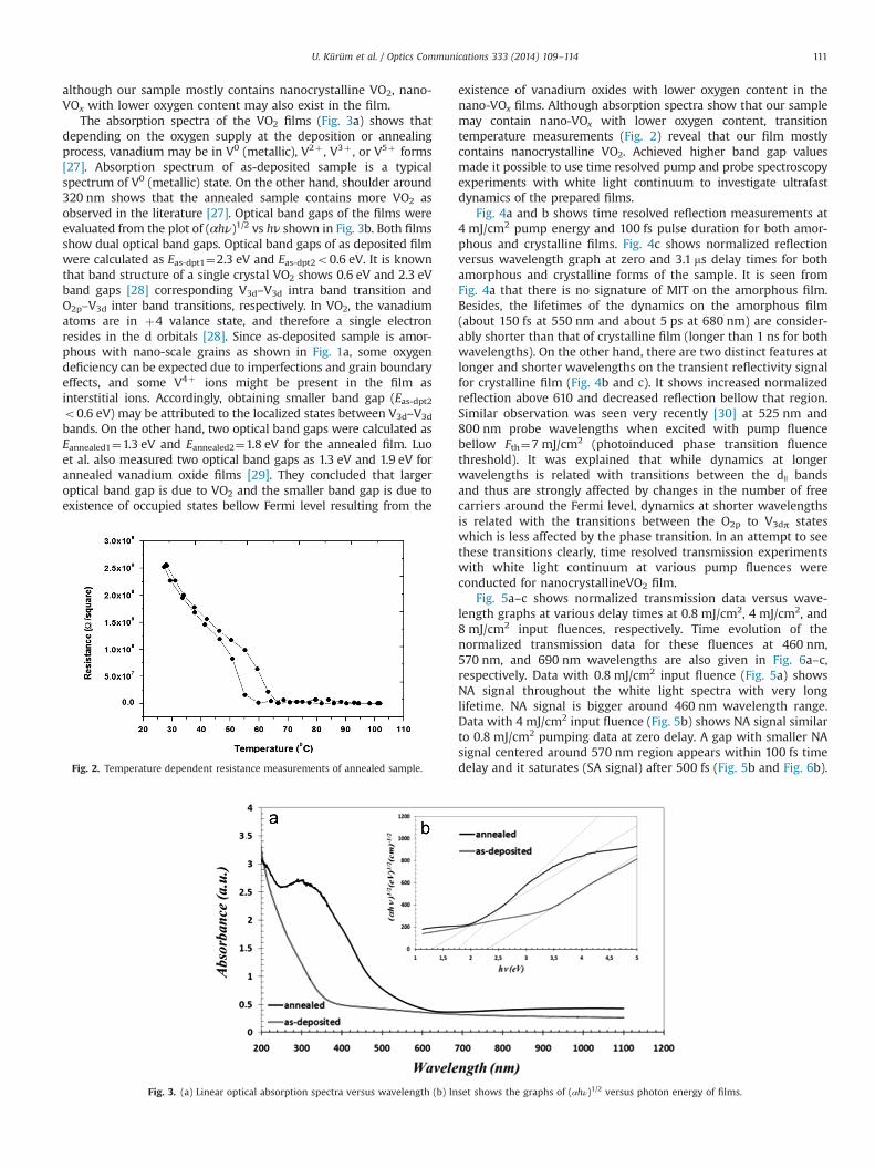
The absorption spectra of the VO2 films (Fig. 3a) shows thatdepending on the oxygen supply at the deposition or annealingprocess, vanadium may be in V0 (metallic), V2þ , V3þ , or V5þ forms[27]. Absorption spectrum of as-deposited sample is a typicalspectrum of V0 (metallic) state. On the other hand, shoulder around320 nm shows that the annealed sample contains more VO2 asobserved in the literature [27]. Optical band gaps of the films wereevaluated from the plot of (αhν)1/2 vs hν shown in Fig. 3b. Both filmsshow dual optical band gaps. Optical band gaps of as deposited filmwere calculated as Eas-dpt1¼2.3 eV and Eas-dpt2o0.6 eV. It is knownthat band structure of a single crystal VO2 shows 0.6 eV and 2.3 eVband gaps [28] corresponding V3d–V3d intra band transition andO2p–V3d inter band transitions, respectively. In VO2, the vanadiumatoms are in þ4 valance state, and therefore a single electronresides in the d orbitals [28]. Since as-deposited sample is amor-phous with nano-scale grains as shown in Fig. 1a, some oxygendeficiency can be expected due to imperfections and grain boundaryeffects, and some V4þ ions might be present in the film asinterstitial ions. Accordingly, obtaining smaller band gap (Eas-dpt2o0.6 eV) may be attributed to the localized states between V3d–V3d
bands. On the other hand, two optical band gaps were calculated asEannealed1¼1.3 eV and Eannealed2¼1.8 eV for the annealed film. Luoet al. also measured two optical band gaps as 1.3 eV and 1.9 eV forannealed vanadium oxide films [29]. They concluded that largeroptical band gap is due to VO2 and the smaller band gap is due toexistence of occupied states bellow Fermi level resulting from the
existence of vanadium oxides with lower oxygen content in thenano-VOx films. Although absorption spectra show that our samplemay contain nano-VOx with lower oxygen content, transitiontemperature measurements (Fig. 2) reveal that our film mostlycontains nanocrystalline VO2. Achieved higher band gap valuesmade it possible to use time resolved pump and probe spectroscopyexperiments with white light continuum to investigate ultrafastdynamics of the prepared films.
Fig. 4a and b shows time resolved reflection measurements at4 mJ/cm2 pump energy and 100 fs pulse duration for both amor-phous and crystalline films. Fig. 4c shows normalized reflectionversus wavelength graph at zero and 3.1 ms delay times for bothamorphous and crystalline forms of the sample. It is seen fromFig. 4a that there is no signature of MIT on the amorphous film.Besides, the lifetimes of the dynamics on the amorphous film(about 150 fs at 550 nm and about 5 ps at 680 nm) are consider-ably shorter than that of crystalline film (longer than 1 ns for bothwavelengths). On the other hand, there are two distinct features atlonger and shorter wavelengths on the transient reflectivity signalfor crystalline film (Fig. 4b and c). It shows increased normalizedreflection above 610 and decreased reflection bellow that region.Similar observation was seen very recently [30] at 525 nm and800 nm probe wavelengths when excited with pump fluencebellow Fth¼7 mJ/cm2 (photoinduced phase transition fluencethreshold). It was explained that while dynamics at longerwavelengths is related with transitions between the d|| bandsand thus are strongly affected by changes in the number of freecarriers around the Fermi level, dynamics at shorter wavelengthsis related with the transitions between the O2p to V3dπ stateswhich is less affected by the phase transition. In an attempt to seethese transitions clearly, time resolved transmission experimentswith white light continuum at various pump fluences wereconducted for nanocrystallineVO2 film.
Fig. 5a–c shows normalized transmission data versus wave-length graphs at various delay times at 0.8 mJ/cm2, 4 mJ/cm2, and8 mJ/cm2 input fluences, respectively. Time evolution of thenormalized transmission data for these fluences at 460 nm,570 nm, and 690 nm wavelengths are also given in Fig. 6a–c,respectively. Data with 0.8 mJ/cm2 input fluence (Fig. 5a) showsNA signal throughout the white light spectra with very longlifetime. NA signal is bigger around 460 nm wavelength range.Data with 4 mJ/cm2 input fluence (Fig. 5b) shows NA signal similarto 0.8 mJ/cm2 pumping data at zero delay. A gap with smaller NAsignal centered around 570 nm region appears within 100 fs timedelay and it saturates (SA signal) after 500 fs (Fig. 5b and Fig. 6b).Fig. 2. Temperature dependent resistance measurements of annealed sample.
Fig. 3. (a) Linear optical absorption spectra versus wavelength (b) Inset shows the graphs of (αhν)1/2 versus photon energy of films.
U. Kürüm et al. / Optics Communications 333 (2014) 109–114 111

While SA signal turns to NA again, NA signals around 460 nm and690 nm region start increasing after 1 ns (Fig. 6a and c, respec-tively). Although the gap with smaller NA signal centered around570 nm region still appear at 8 mJ/cm2 pumping which is above Fth(Fig. 5c and Fig. 6b), it does not turn to saturation. We believe thatabsorption signal turning into a saturation signal within 500 fstime delay around 570 nm region has not been observed experi-mentally. This signal can be explained as followed:
Normalized transmission data can be evaluated qualitatively.Pump pulse excite the system to an intermediate state. Withsufficient optical pumping, relaxation from the intermediate stateto the long lived lower energy non-equilibrium state related to thephotoinduced phase [21,31] takes place. From the photoinducedstate the system finally relaxes to one of the equilibrium states. Thisfinal process occurs usually via heat transfer and therefore has pstimescale. SA signal seen around 570 nm on the normalized trans-mission data at 4 mJ/cm2 input fluence may be related with thesaturation of this long lived non-equilibrium photoinduced state.Since photoinduced phase transition takes place at fluences aboveFth we do not see saturation signal at 570 nm at 8 mJ/cm2 pumpingfluence. On the other hand, nonlinear absorption signal seen at460 nm (Fig. 6a) which is related with the transitions between theO2p to V3dπ states [21] has a very short (a few hundred fs) andlong components. The long component signal increases over time.As seen from Fig. 6a the time evolution of this signal does notchange with input fluence which is due to the fact that transitionsbetween the O2p to V3dπ states are less affected by the phase
transition. However, time evolution of the normalized absorptionsignal seen at 690 nm changes from low pumping (FoFth) to thehigher one (F4Fth). That is because, longer wavelength signals arerelated with transitions between the d|| bands and thus are stronglyaffected by changes in the number of free carriers around the Fermilevel [21].
It is known that transmission chance due to photo inducedphase transition is more pronounced above 900 nm [32]. One ofthe important results of these experiments is that photo inducedphase transition can be seen at wavelength as low as 630 nm(Fig. 4b and c) in our sample. We believe that oxygen content aswell as nano crystalline structure may play important role on thewavelength of photo induced phase transition. More experimentalevidences are needed to clarify this issue. Shifting the photoinduced phase transition wavelength to visible rage is importantfor switching applications requiring visible light.
4. Conclusion
In conclusion, we have prepared nanostructured amorphousVO2 thin film by using pulsed DC magnetron reactive sputtering.Post annealing under vacuum produced nanocrystalline VO2 thinfilm. Evaluation of band gap revealed that nanostructured crystal-line VO2 film has increased and dual band gaps around 1.3 eV and1.8 eV. Due to increased band gap we were able to use pump probe
Fig. 4. Normalized reflection versus wavelengths at 4 mJ/cm2 pump energy for (a) amorphous,(b) crystalline films at various delay times and (c) for both films at zero and3.1 ns delay times.
U. Kürüm et al. / Optics Communications 333 (2014) 109–114112

spectroscopy technique with white light continuum for VO2 thinfilms. Although transmission chance due to photo induced phasetransition of VO2 in the literature usually takes places at infraredregion of the spectrum, broad band time resolved probe spectra inthis work revealed that transmission chance could be observed aslow as 630 nm wavelength. Besides, it was shown that timescales are not only pump fluence dependent, but also wavelengthdependent. These results may be important for applicationsrequiring visible light such as switching. In addition to those,time resolved transmission experiments showed saturation ofabsorption signal region around 570 nm and nonlinear absorption
at shorter and longer wavelengths at 4 mJ/cm2 pump fluence. Thisobserved saturation signal was attributed to the long lived lowerenergy non-equilibrium state related to the photoinduced phase.
Acknowledgments
This work is supported by the Scientific and TechnologicalResearch Council of Turkey (TUBITAK, Project No: TBAG-111T351).
Fig. 5. Normalized transmission versus wavelength graphs of crystalline film at various delay times for (a) 0.8 mJ/cm2, (b) 4 mJ/cm2, and (c) 8 mJ/cm2 input fluences.
Fig. 6. Time evolution of the normalized transmission graphs of crystalline film for (a) 460 nm, (b) 570 nm, and (c) 690 nm wavelengths.
U. Kürüm et al. / Optics Communications 333 (2014) 109–114 113

References
[1] F.J. Morin, Phys. Rev. Lett. 3 (1959) 34.[2] W.R. Roach, I. Balberg, Solid State Commun. 9 (1971) 551.[3] M.F. Becker, R.M. Walser, A.B. Buckman, T. Lapine, P. Georges, A. Brun, Appl.
Phys. Lett. 65 (1994) 1507.[4] A. Cavalleri, Cs. Tóth, C.W. Siders, J.A. Squier, F. Raksi, P. Forget, J.C. Kieffer,
Phys. Rev. Lett. 87 (2001) 237401.[5] P. Baum, D.-S Yang, A.H. Zewail, Science 318 (2007) 788.[6] S.A. Pollack, D.B. Chang, FA. Chudnovsky, I.A. Khakhaev, J. Appl. Phys. 78 (1995)
3592.[7] O.B. Danilov, A.I. Sidorov, Tech. Phys. 44 (1999) 1345.[8] M. Soltani, M. Chaker, E. Haddad, R.V. Kruzelecky, J. Vac. Sci. Technol. A 22
(2004) 859.[9] T.D. Manning, I.P. Parkin, M.E. Pemble, D. Sheel, D. Vernardou, Chem. Mater. 16
(2004) 744.[10] F. Cilento, C. Giannetti, G. Ferrini, S. Dal Conte, T. Sala, G. Coslovich, M. Rini,
A. Cavalleri, F. Parmigiani, Appl. Phys. Lett. 96 (2010) 021102.[11] A. Rúa, F.E. Fernández, N. Sepúlveda, J. Appl. Phys. 107 (2010) 074506.[12] C. Kübler, H. Ehrke, R. Huber, R. Lopez, A. Halabica, R.F. Haglung Jr.,
A. Leitenstorfer, Phys. Rev. Lett. 99 (2007) 116401.[13] A. Cavalleri, M. Rini, H.H.W. Chong, S. Fourmaux, T.E. Glover, P.A. Heimann,
J.C. Kieffer, R.W. Schoenlien, Phys. Rev. Lett. 95 (2005) 067405.[14] A. Cavalleri, Th. Decorsy, H.H.W. Chong, J.C. Kieffer, R.W. Schoenlein, Phys. Rev.
B: Condens. Matter 70 (2004) 161102.[15] H.T. Kim, Y.W. Lee, B.J. Kim, B.G. Chae, S.J. Yun, K.Y. Kang, K.J. Han, K.J. Yee,
Y.S. Lim, Phys. Rev. Lett. 97 (2006) 266401.[16] T.L. Cocker, L.V. Titova, S. Fourmaux, G. Holloway, H.-C Bandulet, D. Brassard,
J.-C Kieffer, M.A. El Khakani, F.A. Hegmann, Phys. Rev. B: Condens. Matter 85(2012) 155120.
[17] S. Wall, D. Brida, S.R. Clark, H. Ehrke, D. Jaksch, A. Ardavan, S. Bonora,H. Uemura, Y. Takahashi, T. Hasegawa, H. Okamoto, G. Cerullo, A. Cavalleri,Nat. Phys. 7 (2011) 114.
[18] C. Giannetti, F. Cilento, S.D. Conte, G. Coslovich, G. Ferrini, M. Molegraaf,H. Raichle, R. Liang, H. Eisaki, M. Greven, A. Damascelli, D. van der Marel,F. Parmigiani, Nat. Commun. 2 (2011) 353.
[19] S. Dal Conte, C. Giannetti, G. Goslovich, F. Cilento, D. Bossini, T. Abebaw,F. Banfi, G. Ferrini, H. Eisaki, M. Greven, A. Damascelli, D. van der Marel,F. Parmigiani, Science 335 (2012) 1600.
[20] S.K. Sundaram, E. Mazur, Nat. Mater. 1 (2002) 217.[21] S. Wall, L. Foglia, D. Wegkamp, K. Appavoo, J. Nag, R.F. Haglung, J. Stahler,
M. Wolf, Phys. Rev. B: Condens. Matter 87 (2013) 115126.[22] H.W. Verluer, A.S. Barker, C.N. Berlung, Phys. Rev. 172 (1968) 788.[23] Y. Wang, Z. Zhang, Y. Zhu, Z. Li, R. Vajtai, L. Ci, PM. Ajayan, ACS Nano 2 (7)
(2008) 1492.[24] L. Zhenfei, W. Zhiming, X. Xiangdong, W. Tao, J. Yadong, Thin Solid Films 519
(19) (2011) 6203.[25] R.M. Oksuzoglu, P. Bilgic, M. Yıldırım, O. Deniz, Opt. Laser Technol. 48 (2013)
102.[26] B.G. Chae, H.T. Kim, Physica B 405 (2010) 663.[27] H. Liu, O. Vasquez, V.R. Santiago, L. Dıaz, F.E. Fernandez, J. Lumin. 108 (2004)
233.[28] M.M. Qazilbash, A.A. Schafgans, K.S. Burch, S.J. Yun, B.G. Chae, B.J. Kim,
H.T. Kim, D.N. Basov, Phys. Rev. B: Condens. Matter 77 (2008) 115121.[29] Z. Luo, Z. Wu, X. Xu, T. Wang, Y. Jiang, Thin Solid Films 519 (2011) 6203.[30] S. Wall, D. Wegkamp, L. Foglia, K. Appavoo, J. Nag, R.F. Haglung, J. Stahler,
M. Wolf, Nat. Commun. 3 (2012) 721.[31] L. Foglia, Ph.D. Thesis, Freie Universität Berlin, (2011).[32] J. Leroy, A. Bessaudou, F. Cosset, A. Crunteanu, Thin Solid Films 520 (2012)
4823.
U. Kürüm et al. / Optics Communications 333 (2014) 109–114114
Copyright © 2022 FDOKUMEN