Dislocation Configurations in Nanocrystalline FeMo Sintered Components
6
Dislocation Configurations in Nanocrystalline FeMo Sintered Components PAOLO SCARDI, MIRCO D’INCAU, MATTEO LEONI, and ALESSANDRO FAIS Net-shape compaction of a nanocrystalline ball-milled commercial Fe-1.5 wt pct Mo powder was done via spark plasma sintering (SPS) and capacitor discharge sintering (CDS). A detailed microstructure analysis, performed by X-ray diffraction–whole powder pattern modeling (XRD-WPPM), shows that CDS, owing to the faster sintering conditions, retains a much finer and more uniform microstructure with dislocations uniformly distributed inside the nanocrys- talline grains. Conversely, SPS causes dislocations to pile up and extensive grain growth to occur, especially when high sintering temperatures are employed. DOI: 10.1007/s11661-009-9987-x Ó The Minerals, Metals & Materials Society and ASM International 2009 I. INTRODUCTION ONE of the challenges in metal powder sintering technology is how to transfer the peculiar properties of nanocrystalline materials to compacted components. This has become of special interest in recent years, in which extensive research has been devoted to the pro- duction of nanocrystalline, heavily deformed metal powders and their compaction by advanced sintering techniques. [1–4] The best processing conditions—highest (i.e. theoretical) density in the sintered component, while preserving as much as possible the fine grain size and high lattice defect density of the starting nanopowder—can hardly be achieved by conventional sintering. [2,5] Within the large family of field-assisted sintering techniques (FAST) or electric current activated sintering (ECAS), spark plasma sintering (SPS) has been studied in some detail. [6] Despite the good results reported in the literature, [7,8] sintering time is still on the order of minutes and the process is controlled in temperature, with an electronic feedback, thus allowing for a certain degree of thermal equilibrium to be reached. Despite undisputed improvements with respect to traditional techniques, the relatively high sintering temperatures required to reach high densities tend to anneal the microstructure, thus losing at least part of the properties of the starting powders. [1,2] Although suitable additions may be used to stabilize the nanostructure and to reduce the damaging effect of high temperature/long process time, [9] substantial improvements should probably involve a different approach. Key factors such as rapidity and effectiveness of the sintering process seem to be peculiar to another family of FASTs, known as single-pulse techniques, or electrodis- charge sintering (EDS). Electrodischarge sintering requires a single, short pulse of electromagnetic energy to sinter the powder compacts while applying mechanical pressure. [10] A recently developed EDS technique, named capacitor discharge sintering (CDS), is based on a single pulse of low voltage, high current electromagnetic energy, delivered in a short time (tens of milliseconds) to powders in a conducting mold previously loaded with mechanical pressure. Capacitor discharge sintering, com- pared to traditional EDS, [11–14] employs low voltages (from 5 to 30 V) and is composed of two mutually coupled freely oscillating circuits with a solid-state switch on the primary circuit analogous to those used in capacitor discharge welding. The output voltage closely resembles another EDS named high energy-high rate (HEHR), [15,16] but the sintering/discharge time is only 20 to 30 ms in CDS compared to 3 seconds in HEHR. Preliminary studies have already proved the effectiveness of CDS in compacting several metal powders. [17–19] The present article provides a comparison between SPS and CDS of a typical metal system, a Mo-stabilized iron alloy. Since the main differences between SPS and CDS components are in the microstructure, namely, the crystalline domain size and lattice defects density, an advanced X-ray diffraction (XRD) line profile analysis (LPA) method is used. Whole powder pattern modeling (WPPM) [20–23] provides information on crystalline domain size and dispersion, and on the density and distribution of dislocations in the ferritic iron phase. Correlations with two basic macroscopic properties, density and microhardness, are discussed. II. EXPERIMENTAL Fe-1.5 wt pct Mo powders were ground at increasing times, for 8, 32, 64, 96, and 128 hours (Reference 24 for PAOLO SCARDI, Professor, and MIRCO D’INCAU and MATTEO LEONI, Doctors, are with the Department of Materials Engineering and Industrial Technologies, University of Trento, 38100 Trento, Italy. Contact e-mail: [email protected] ALESSANDRO FAIS, Doctor, is with the Department of Materials Science and Chemical Engineering, Turin Polytechnic, 10129 Torino, Italy. This article is based on a presentation given in the symposium ‘‘Neutron and X-Ray Studies of Advanced Materials,’’ which occurred February 15–19, 2009, during the TMS Annual Meeting in San Francisco, CA, under the auspices of TMS, TMS Structural Materials Division, TMS/ASM Mechanical Behavior of Materials Committee, TMS: Advanced Characterization, Testing, and Simulation Commit- tee, and TMS: Titanium Committee. METALLURGICAL AND MATERIALS TRANSACTIONS A
-
Upload
independent -
Category
Documents
-
view
0 -
download
0
Transcript of Dislocation Configurations in Nanocrystalline FeMo Sintered Components

Dislocation Configurations in Nanocrystalline FeMo SinteredComponents
PAOLO SCARDI, MIRCO D’INCAU, MATTEO LEONI, and ALESSANDRO FAIS
Net-shape compaction of a nanocrystalline ball-milled commercial Fe-1.5 wt pct Mo powderwas done via spark plasma sintering (SPS) and capacitor discharge sintering (CDS). A detailedmicrostructure analysis, performed by X-ray diffraction–whole powder pattern modeling(XRD-WPPM), shows that CDS, owing to the faster sintering conditions, retains a much finerand more uniform microstructure with dislocations uniformly distributed inside the nanocrys-talline grains. Conversely, SPS causes dislocations to pile up and extensive grain growth tooccur, especially when high sintering temperatures are employed.
DOI: 10.1007/s11661-009-9987-x� The Minerals, Metals & Materials Society and ASM International 2009
I. INTRODUCTION
ONE of the challenges in metal powder sinteringtechnology is how to transfer the peculiar properties ofnanocrystalline materials to compacted components.This has become of special interest in recent years, inwhich extensive research has been devoted to the pro-duction of nanocrystalline, heavily deformed metalpowders and their compaction by advanced sinteringtechniques.[1–4] The best processing conditions—highest(i.e. theoretical) density in the sintered component, whilepreserving as much as possible the fine grain size and highlattice defect density of the starting nanopowder—canhardly be achieved by conventional sintering.[2,5]
Within the large family of field-assisted sinteringtechniques (FAST) or electric current activated sintering(ECAS), spark plasma sintering (SPS) has been studiedin some detail.[6] Despite the good results reported in theliterature,[7,8] sintering time is still on the order ofminutes and the process is controlled in temperature,with an electronic feedback, thus allowing for a certaindegree of thermal equilibrium to be reached. Despiteundisputed improvements with respect to traditionaltechniques, the relatively high sintering temperaturesrequired to reach high densities tend to anneal themicrostructure, thus losing at least part of the propertiesof the starting powders.[1,2] Although suitable additionsmay be used to stabilize the nanostructure and to reducethe damaging effect of high temperature/long process
time,[9] substantial improvements should probablyinvolve a different approach.Key factors such as rapidity and effectiveness of the
sintering process seem to be peculiar to another family ofFASTs, known as single-pulse techniques, or electrodis-charge sintering (EDS). Electrodischarge sinteringrequires a single, short pulse of electromagnetic energyto sinter the powder compacts while applying mechanicalpressure.[10] A recently developed EDS technique, namedcapacitor discharge sintering (CDS), is based on a singlepulse of low voltage, high current electromagneticenergy, delivered in a short time (tens of milliseconds)to powders in a conducting mold previously loaded withmechanical pressure. Capacitor discharge sintering, com-pared to traditional EDS,[11–14] employs low voltages(from 5 to 30 V) and is composed of two mutuallycoupled freely oscillating circuits with a solid-state switchon the primary circuit analogous to those used incapacitor discharge welding. The output voltage closelyresembles another EDS named high energy-high rate(HEHR),[15,16] but the sintering/discharge time is only 20to 30 ms in CDS compared to 3 seconds in HEHR.Preliminary studies have already proved the effectivenessof CDS in compacting several metal powders.[17–19]
The present article provides a comparison betweenSPS and CDS of a typical metal system, a Mo-stabilizediron alloy. Since the main differences between SPS andCDS components are in the microstructure, namely, thecrystalline domain size and lattice defects density, anadvanced X-ray diffraction (XRD) line profile analysis(LPA) method is used. Whole powder pattern modeling(WPPM)[20–23] provides information on crystallinedomain size and dispersion, and on the density anddistribution of dislocations in the ferritic iron phase.Correlations with two basic macroscopic properties,density and microhardness, are discussed.
II. EXPERIMENTAL
Fe-1.5 wt pct Mo powders were ground at increasingtimes, for 8, 32, 64, 96, and 128 hours (Reference 24 for
PAOLO SCARDI, Professor, and MIRCO D’INCAU andMATTEO LEONI, Doctors, are with the Department of MaterialsEngineering and Industrial Technologies, University of Trento, 38100Trento, Italy. Contact e-mail: [email protected] ALESSANDROFAIS, Doctor, is with the Department of Materials Science andChemical Engineering, Turin Polytechnic, 10129 Torino, Italy.
This article is based on a presentation given in the symposium‘‘Neutron and X-Ray Studies of Advanced Materials,’’ which occurredFebruary 15–19, 2009, during the TMS Annual Meeting in SanFrancisco, CA, under the auspices of TMS, TMS Structural MaterialsDivision, TMS/ASM Mechanical Behavior of Materials Committee,TMS: Advanced Characterization, Testing, and Simulation Commit-tee, and TMS: Titanium Committee.
METALLURGICAL AND MATERIALS TRANSACTIONS A

details). Milled powders were capacitor-discharge sin-tered into small disks of 2 g inside a graphite mold withmetallic plungers/electrodes, which applied a nominalpressure of 250 MPa and with different specific energyinputs (SEIs) from 1.3 to 3.4 kJ/g. The SPS of thedifferent powders was carried out at 600 �C, 650 �C,700 �C, 750 �C, and 800 �C, with a heating rate totemperature of 50 �C/min (respectively 13, 14, 15, 16,and 17 minutes) in graphite punches and dies and anominal pressure of 76 MPa. All samples where diskswith a radius of 10 mm. The densities were evaluatedwith Archimede’s principle, while Vickers micro-hardness was obtained, after polishing, from the meanvalue of 8 to 12 hardness measurements done in twodifferent laboratories with a force of 300 and of 50 gfand a hold time of 15 seconds.[17,25]
To avoid including contributions from polishing,before XRD measurements, all specimens were chemi-cally thinned using a solution of nitric acid (4 pct)-orthophosphoric acid (80 pct). The XRD patterns werecollected at each layer removal stage (approximately20 lm), until no changes were observed after furtherremoval.
III. WHOLE POWDER PATTERN MODELING
The observed (h) diffraction profile can be thought ofas a convolution of instrumental (g) and specimen-related (f) profile components.[26] Fourier analysis isespecially useful to deal with this case, as the complexproblem of handling a convolution integral can beturned into the relatively simpler one of a Fourierintegral:[20,21]
I s; shklð Þ /X
hkl
whkl
ZChkl Lð Þ exp 2piL s� shklð Þ½ �dL ½1�
where s is the reciprocal space variable, and shkl is sin Bragg condition, including possible shifts due tolattice defects (e.g., faulting). Since the latter may dif-ferently affect the various equivalent points in recipro-cal space, the observed powder diffraction profileresults from the sum of Fourier integrals for all hklequivalent combinations, with a weight whkl. Chkl isthe product of the Fourier transforms (FTs) of eachprofile component:
Chkl ¼ TIP�AS�AF�AD�AAPB� . . . ½2�
where TIP groups all contributions to the g profile, andthe other terms (A) refer to f components. The latter areknown—in many cases, in closed analytical form—forseveral contributing effects, such as domain shape andsize distributions (AS), dislocations (AD), planar defects(AF), antiphase boundaries (AAPB), etc. Virtually anyother contributing effect can be included by adding(multiplying in Eq. [2]) the corresponding FT.[20–23]
The g component can be handled by a fundamentalparameters approach[27] or, more simply, through aparameterization of the experimental pattern of asuitable line profile standard (e.g., LaB6 SRM 660a
distributed by NIST; e.g., see Reference 23 for details),so it is in any case a known quantity. In the present caseof study, the phase of interest is a bcc metal (a-Fe) forwhich we can expect the main contribution to the fprofile to come from the fine size of crystalline domains(AS) and dislocations (AD). For the ‘‘size’’ effect, wecan assume that the approximately equiaxial domainscan be represented by spherical crystallites whosediameters follow a lognormal distribution with meanl and variance r.[20–22] Concerning dislocations, theKrivoglaz–Wilkens theory[28–30] is still the most appro-priate one to model the effect of a system of dislocationswith an average density q (assuming equally a populated1�10� �
111h i slip system) and an effective outer cut-offradius Re.
[29,30] Expressions for the FT can be evaluatedboth for screw and for edge dislocations, for which it ispossible to calculate the corresponding average ‘‘‘visi-bility’’ effect, or contrast factor,[28–32] which representsthe anisotropic line broadening effect of the line defectand of the crystalline medium.Diffraction peak profiles can then be modeled by
adjusting (by nonlinear least squares) just a few micro-structural parameters, which in this case are q, Re, thedislocation character (fE, edge/screw fraction), l, and rof the domain size distribution. Additional parametersare used to reproduce a background, unit cell param-eters, and some common aberrations of the powdergeometry. Peak intensities are usually considered as freeparameters, but they can also be constrained accordingto a structural model, as in the Rietveld method.[33] Ifthis is the case, WPPM also provides for a quantitativephase analysis, of interest in phase mixtures.For further details and a survey of WPPM applica-
tions, see Reference 23 and the references therein.
IV. RESULTS AND DISCUSSION
Figure 1 shows an example of WPPM for a FeMosintered component. In this specific case (CDS 64 hour),
Fig. 1—WPPM results for CDS 64-h sintered component: experi-mental data (dot), model (line), and their difference (residual, linebelow). The inset shows a logarithmic plot, with indications of themost intense lines of the c-Fe minority fraction (arrows).
METALLURGICAL AND MATERIALS TRANSACTIONS A

as in the other cases discussed subsequently, a minorfraction of c-Fe (arrows) appears together with the maina-Fe phase. Minor amounts of iron oxide (magnetite)were also found in several sintered components. AsWPPM supports the analysis of all phases, allowing alsofor a quantification of the relative fractions, microstruc-tural results for the main phase of interest, a-Fe, arenearly unaffected by the presence of other phases. Themain results of WPPM are summarized in Figure 2,where average dislocation density ((a) and (b)) and meandomain size ((c) and (d)) are shown as a function ofsintering temperature (T in �C) and SEI (in J/g),respectively, for SPS and CDS components.
As a general trend, dislocation density tends todecrease with the SPS temperature, the diminutionbeing more evident for 96- and 128-hour powderssintered above 750 �C. Correspondingly, the domainsize increases, with a marked growth above 750 �C. Thedomain sizes for SPS at 800 �C are of several hundredsof nanometers, close to, or possibly above, valuesreliably accessible to XRD LPA. The overall result isthat the nanostructure is preserved up to sinteringtemperatures of 750 �C, with the powders ball milled for128 hours preserving a proportionally higher dislocation
density/smaller domain size than the powders groundfor shorter time. Above 750 �C, extensive grain growthand defect annealing takes place.Capacitor discharge sintering also causes a marked
decrease in dislocation density, the difference betweendifferent powders decreasing for increasing SEI. Themain difference with respect to SPS seems to be thedomain size, never exceeding 100 to 150 nm, even forthe highest SEI employed. According to this informa-tion, CDS seems to better preserve the nanostructurethan SPS. Electron microscopy supports this hypothesis.As shown in Figure 3, CDS gives a uniform, fine-grained (<1 lm) microstructure, whereas SPS clearlyshows a coarser microstructure. The bimodality of theSPS grain size distribution is also evident, with scatteredregions of fine grains (submicron size) separated bylarger grains (5 to 10 lm). This feature of the SPS hasalready been observed[34,35] and can partly be controlledby varying (increasing) the pressure.As a potential drawback of the CDS, a minor but
clearly measurable fraction of austenitic phase isformed. As shown in Figure 4, the amount of austenitetends to increase for increasing SEI, and the effect ismore visible for the most extensively ball-milled pow-
(a) (b)
(d)(c)
Fig. 2—WPPM results. (a) and (b) Average dislocation density and (c) and (d) mean domain size as a function of sintering temperature or SEI,respectively, for SPS or CDS components obtained from powders ball milled for 128 h (square), 96 h (circle), 64 h (rhomb), and 32 h (triangle).Lines are drawn just to drive the eye. Data points at T = 0 and SEI = 0 refer to the ball-milled powders, before sintering.
METALLURGICAL AND MATERIALS TRANSACTIONS A
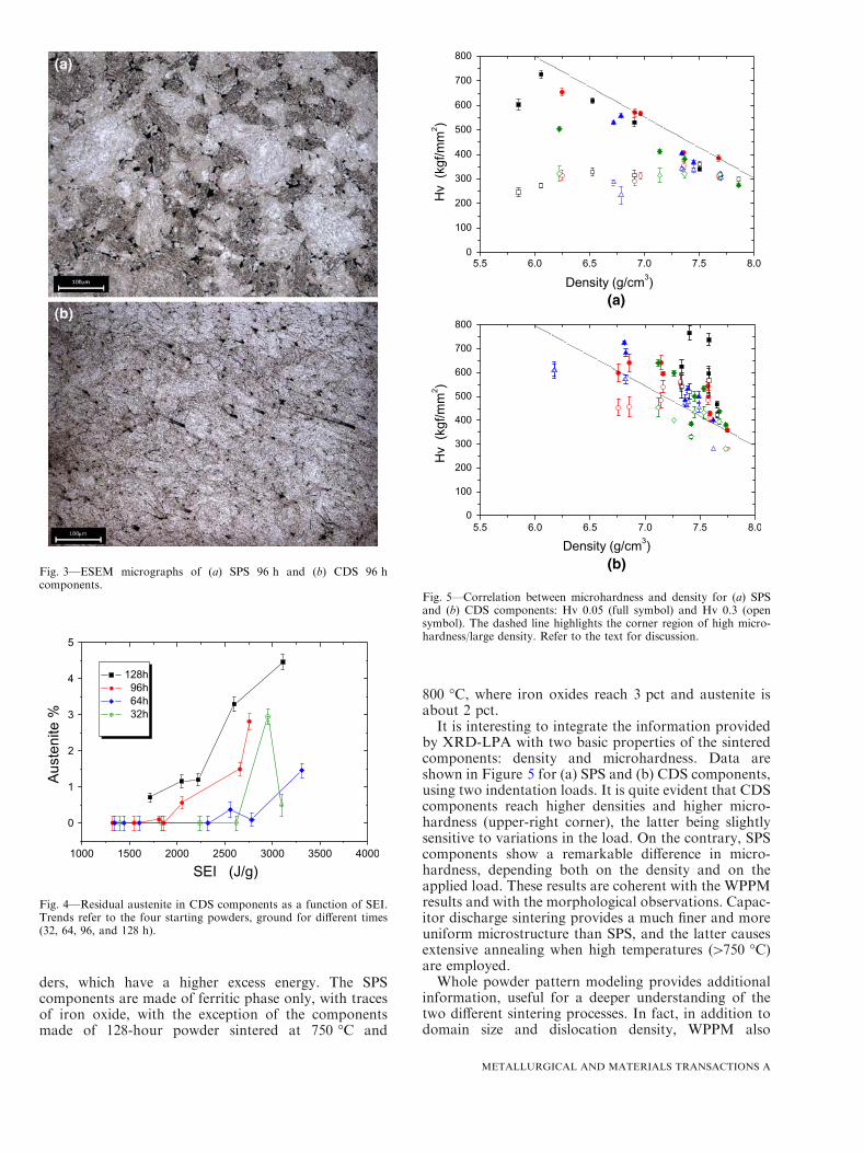
ders, which have a higher excess energy. The SPScomponents are made of ferritic phase only, with tracesof iron oxide, with the exception of the componentsmade of 128-hour powder sintered at 750 �C and
800 �C, where iron oxides reach 3 pct and austenite isabout 2 pct.It is interesting to integrate the information provided
by XRD-LPA with two basic properties of the sinteredcomponents: density and microhardness. Data areshown in Figure 5 for (a) SPS and (b) CDS components,using two indentation loads. It is quite evident that CDScomponents reach higher densities and higher micro-hardness (upper-right corner), the latter being slightlysensitive to variations in the load. On the contrary, SPScomponents show a remarkable difference in micro-hardness, depending both on the density and on theapplied load. These results are coherent with the WPPMresults and with the morphological observations. Capac-itor discharge sintering provides a much finer and moreuniform microstructure than SPS, and the latter causesextensive annealing when high temperatures (>750 �C)are employed.Whole powder pattern modeling provides additional
information, useful for a deeper understanding of thetwo different sintering processes. In fact, in addition todomain size and dislocation density, WPPM also
Fig. 3—ESEM micrographs of (a) SPS 96 h and (b) CDS 96 hcomponents.
Fig. 4—Residual austenite in CDS components as a function of SEI.Trends refer to the four starting powders, ground for different times(32, 64, 96, and 128 h).
(a)
(b)
Fig. 5—Correlation between microhardness and density for (a) SPSand (b) CDS components: Hv 0.05 (full symbol) and Hv 0.3 (opensymbol). The dashed line highlights the corner region of high micro-hardness/large density. Refer to the text for discussion.
METALLURGICAL AND MATERIALS TRANSACTIONS A

provides the effective outer cut-off radius, which can beconveniently combined with the dislocation density inthe so-called Wilkens parameter, M ¼ Re
ffiffiffiqp
. The latteris shown in Figure 6 for SPS (open symbols) and CDS(full symbols) components, as a function of the dislo-cation density. It is worth noting that, in this plot,movement from right to left (i.e., for decreasing dislo-cation density) corresponds to components sintered atincreasing SEI (CDS) and increasing T (SPS). The valueof M tends to decrease after the SPS process, whereas itincreases markedly after CDS. According to the theoryof the line broadening effects of dislocations,[28–30] Mvalues close to (and below) unity are observed whendislocations are strongly interacting, as in dipole con-figurations or in dislocation walls: this is the case for theSPS components, as the result of near thermal equilib-rium process conditions, and could be the result of atendency of dislocations to pileup and reach lowerenergy configurations, as in all temperature-activatedsintering processes. A Wilkens parameter well aboveunity, instead, may result from randomly disperseddislocations. This is the case observed in CDS compo-nents, where the fast sintering conditions push thesystem very far from equilibrium, with the dislocationsremaining ‘‘frozen’’ in a random distribution inside thecrystalline domains.
It is therefore concluded that, although the averagedislocation density after SPS and CDS is similar, thedistribution of the dislocations is probably different, andmight contribute to an explanation of the highermicrohardness observed for CDS components withrespect to SPS components with similar density andmean domain size. This observation confirms analogousresults obtained in a sensibly different system such aspure copper[19] and is still the object of ongoing researchactivity.
As a final remark, this article shows that XRD LPA,following a WPPM approach, provides detailed infor-mation on the microstructure of sintered componentsfrom nanocrystalline metal powders. Information isgiven on the domain size as well as on the density andpossible arrangement of line defects. The same approachcan be used for any type of crystalline material, as theapplicability of the model has recently been extended tosystems with any crystal symmetry,[31,32] and can alsoaccount for other microstructural features and latticedefects that produce measurable effects on the diffrac-tion line profile.[23]
ACKNOWLEDGMENT
The authors thank Dr. M. Zadra for the precioussupport in the preparation of SPS components.
REFERENCES1. H.J. Fecht: in Nanostructured Materials and Composites Prepared
by Solid State Processing, C.C. Koch, ed., Noyes Publications,Norwick, NY, 2002, pp. 73–113.
2. J.R. Groza: in Nanostructured Materials and Composites Preparedby Solid State Processing, C.C. Koch, ed., Noyes Publications,Norwick, NY, 2002, pp. 115–78.
3. C. Suryanarayana: Prog. Mater. Sci., 2001, vol. 46, pp. 1–184.4. R.Z. Valiev, R.K. Islamgaliev, and I.V. Alexandrov: Prog. Mater.
Sci., 2000, vol. 45, p. 103.5. C.C. Koch: J. Mater. Sci., 2007, vol. 42, pp. 1403–14.6. J. Rawers: Nanostruct. Mater., 1999, vol. 11 (4), pp. 513–22.7. K.Y. Sastry, L. Froyen, J. Vleugels, O. Van der Biest,
R. Schattevoy, and J. Hennicke: Rev. Adv. Mater. Sci., 2004,vol. 8 (1), pp. 27–32.
8. K.Y. Sastry, L. Froyen, J. Vleugels,O.Van derBiest, R. Schattevoy,and K. Hummert: Mater. Sci. Forum, 2006, vols. 519–521,pp. 1409–14.
9. S. Libardi, M. Leoni, L. Facchini, M. D’Incau, P. Scardi, and A.Molinari: Mater. Sci. Eng. A, 2007, vols. 445–446, pp. 244–50.
10. R. Orru, R. Licheri, A.M. Locci, A. Cincotti, and G. Cao: Mater.Sci. Eng. R, 2009, vol. 63, pp. 127–288.
11. S. Clyens, S.T.S. Al-Hassani, and W. Johnson: Int. J. Mech. Sci.,1976, vol. 18 (1), pp. 37–44.
12. T. Alp, S.T.S. Al-Hassani, and W. Johnson: J. Eng. Mater.Technol., 1985, vol. 107, p. 109.
13. W. Johnson, S. Clyens, and S.T.S. Al-Hassani: Metallurgia Met.Form., 1976, vol. 43, p. 82.
14. M. Shakery, S.T.S. Al-Hassani, and T.J. Davis: Powder Metall.Int., 1979, vol. 11 (3), pp. 120–25.
15. D.R. Ervin, D.L. Bourell, C. Persad, and L. Rabenberg: Mater.Sci. Eng. A, 1988, vol. 102, pp. 25–30.
16. S.L. Raghunathan, C. Persad, D.L. Bourell, and H.L. Marcus:Mater. Sci. Eng. A, 1991, vol. 131, pp. 243–53.
17. A. Fais: Ph.D. Thesis, Turin Polytechnic, Turin, 2008.18. A. Fais and G. Maizza: J. Mater. Proc. Technol., 2008, vol. 202,
pp. 70–75.19. A. Fais and P. Scardi: Z. Kristallogr. Suppl., 2008, vol. 27,
pp. 37–44.20. P. Scardi and M. Leoni: Acta Cryst. A, 2001, vol. 57, pp. 604–13.21. P. Scardi and M. Leoni: Acta Cryst. A, 1002, vol. 58, pp. 190–200.22. M. Leoni and P. Scardi: J. Appl. Cryst., 2004, vol. 37, pp. 629–34.23. P. Scardi: in Powder Diffraction: Theory and Practice, R.E.
Dinnebier and S.J.L. Billinge, eds., The Royal Society ofChemistry, Cambridge, United Kingdom, 2008, pp. 376–413.
24. M. D’Incau, M. Leoni, and P. Scardi: J. Mater. Res., 2007, vol. 22,pp. 1744–53.
25. M. D’Incau: Ph.D. Thesis, University of Trento, Trento, 2008.26. H.P. Klug and L.E. Alexander: X-ray Diffraction Procedures for
Polycrystalline and Amorphous Materials, Wiley, New York, NY,1974.
Fig. 6—Correlation between the Wilkens parameter (M ¼ Reffiffiffiqp
)and average dislocation density (q) for CDS (full symbols) and SPS(open symbols) components obtained from nanocrystalline FeMopowders ground for different times: 128 h (square), 96 h (circle), and64 h (triangle). Full symbols in gray on the right side (after thex-axis break) refer to the starting powders. Lines are drawn just tohighlight the overall trend.
METALLURGICAL AND MATERIALS TRANSACTIONS A

27. R.W. Cheary and A. Coelho: J. Appl. Cryst., 1992, vol. 25,pp. 109–21.
28. M.A. Krivoglaz and K.P. Ryaboshapka: Fiz. Metall., 1963,vol. 15, pp. 18–28.
29. M. Wilkens: Phys. Status Solidi A, 1970, vol. 2, pp. 359–70.30. M. Wilkens: Fundamental Aspects of Dislocation Theory, J.A.
Simmons, R. de Wit, and R. Bullough, eds., National Bureau ofStandards (US) Special Publication No. 317, NBS, Washington,DC, vol. II, pp. 1195–1221.
31. M. Leoni, J. Martinez-Garcia, and P. Scardi: J. Appl. Cryst., 2007,vol. 40, pp. 719–24.
32. J. Martinez-Garcia, M. Leoni, and P. Scardi: Acta Cryst. A, 2009,vol. 65, pp. 109–19.
33. R.A. Young: The Rietveld Method, Oxford University Press,Oxford, United Kingdom, 1993.
34. S. Kawamura and H. Kuwano: J. Jpn. Soc. Powder Metall., 2003,vol. 50 (7), pp. 545–50.
35. S. Kawaura, H. Kuwano, Y. Takeda, S. Takahashi, and H. Kaga:J. Jpn. Soc. Powder Metall., 2003, vol. 50 (12), pp. 1052–56.
METALLURGICAL AND MATERIALS TRANSACTIONS A