Ultra-thin nanocrystalline lanthanum strontium cobalt ferrite (La 0.6Sr 0.4Co 0.8Fe 0.2O 3− δ )...
8
Journal of Power Sources 186 (2009) 115–122 Contents lists available at ScienceDirect Journal of Power Sources journal homepage: www.elsevier.com/locate/jpowsour Ultra-thin nanocrystalline lanthanum strontium cobalt ferrite (La 0.6 Sr 0.4 Co 0.8 Fe 0.2 O 3−ı ) films synthesis by RF-sputtering and temperature-dependent conductivity studies Bo-Kuai Lai, Alex C. Johnson, Hui Xiong, Shriram Ramanathan ∗ Harvard School of Engineering and Applied Sciences, Harvard University, Cambridge, MA 02138, USA article info Article history: Received 18 August 2008 Received in revised form 22 September 2008 Accepted 23 September 2008 Available online 4 October 2008 Keywords: Lanthanum strontium cobalt ferrite Yttria-stabilized zirconia Solid oxide fuel cell Cathode Ultra-thin film Nanocrystalline abstract Nanocrystalline lanthanum strontium cobalt ferrite (LSCF) ultra-thin films with high in-plane electri- cal conductivity have been deposited by RF sputtering from composite targets. The films, with nominal thickness of 54nm, are crystalline when annealed or deposited at temperatures above 450 ◦ C. Effects of annealing temperature, annealing time, and substrate temperature on crystallization, microstructure, and room temperature lateral electrical conductivity have been systematically studied. No interfacial reaction products between the LSCF and single crystalline yttria-stabilized zirconia (YSZ) were observed from X-ray diffraction studies upon annealing until 750 ◦ C. In-plane electrical conductivity as high as 580 S cm −1 at 650 ◦ C has been observed for LSCF thin films deposited on single crystalline YSZ substrates and sputtered nanocrystalline YSZ thin films; while activation energy for conductivity were determined to be 0.15eV and 0.10eV for the former and latter films, respectively, in 650–400 ◦ C range. The high in-plane electrical conductivity for the nanocrystalline LSCF ultra-thin films is likely attributed to their low level of porosity. Micro-solid oxide fuels cells using 15nm thick LSCF films as cathodes and sub- 100nm yttria-doped zirconia thin film electrolytes have been fabricated successfully and demonstrated to achieve peak power density of 60 mW cm −2 at 500 ◦ C. Our results demonstrate that RF sputtering pro- vides a low-temperature synthesis route for realizing ultra-thin nanocrystalline LSCF films as cathodes for intermediate- or low-temperature solid oxide fuel cells. © 2008 Elsevier B.V. All rights reserved. 1. Introduction With increasing demand for energy coupled with finite reserve of fossil fuels and coals, it is imperative to develop sustainable, alternative energy sources. Hydrogen (or hydrocarbon)-fueled solid oxide fuel cells (SOFCs), with energy efficiency higher than 60% and clean emissions, represents a promising energy alternative [1]. They can be used in stationary power plants to replace coals and in automobiles to replace gasoline [2]. By taking advantage of well-established microfabrication techniques, low-cost micro- SOFCs (SOFCs) for portable electronics have also stimulated considerable attention [3–6]. The hurdles that have yet to overcome for current SOFCs development are their high temperature operation (>900 ◦ C) and, consequently, high cost and long-term durability issues [7]. To lower operation temperature, cathodes need special attention because they are responsible for majority of voltage loss in SOFCs ∗ Corresponding author. E-mail address: [email protected] (S. Ramanathan). [8,9]. Three approaches have usually been pursued to improve cathode performance at low temperatures: (i) using new cathode materials to replace conventional lanthanum strontium mangan- ite (LSM) – which does not provide sufficient ionic conductivity below 800 ◦ C [10–12]; (ii) using thinner cathode layer to reduce Ohmic resistance [11,12]; and (iii) using nanocrystalline microstruc- tures to enhance oxygen-ion diffusion through the cathode via grain boundaries [13]. Lanthanum strontium cobalt ferrite (LSCF) has long been con- sidered as one of the most promising cathode materials [14] for low-temperature operation due to its high mixed ionic and elec- tronic conductivities and high electrocatalytic activity of oxygen reduction reaction that occurs on entire cathode surfaces rather than only at three phase boundaries. As a result, thin dense films could provide comparable or higher cathode performance than conventional thick porous films [15,16]. However, there are several technological and fundamental challenges for realizing LSCF thin film cathodes for SOFCs. Firstly, most of synthesis methods for LSCF thin films involve high temperature treatment (>800 ◦ C) [13,17,18] that may lead to resistive interfacial reaction products, such as La 2 Zr 2 O 7 and SrZrO 3, with yttria-stabilized zirconia (YSZ) – one 0378-7753/$ – see front matter © 2008 Elsevier B.V. All rights reserved. doi:10.1016/j.jpowsour.2008.09.094
-
Upload
independent -
Category
Documents
-
view
1 -
download
0
Transcript of Ultra-thin nanocrystalline lanthanum strontium cobalt ferrite (La 0.6Sr 0.4Co 0.8Fe 0.2O 3− δ )...
U(t
BH
a
ARR2AA
KLYSCUN
1
oaoa[aoSc
dclb
0d
Journal of Power Sources 186 (2009) 115–122
Contents lists available at ScienceDirect
Journal of Power Sources
journa l homepage: www.e lsev ier .com/ locate / jpowsour
ltra-thin nanocrystalline lanthanum strontium cobalt ferriteLa0.6Sr0.4Co0.8Fe0.2O3−ı) films synthesis by RF-sputtering andemperature-dependent conductivity studies
o-Kuai Lai, Alex C. Johnson, Hui Xiong, Shriram Ramanathan ∗
arvard School of Engineering and Applied Sciences, Harvard University, Cambridge, MA 02138, USA
r t i c l e i n f o
rticle history:eceived 18 August 2008eceived in revised form2 September 2008ccepted 23 September 2008vailable online 4 October 2008
eywords:anthanum strontium cobalt ferritettria-stabilized zirconia
a b s t r a c t
Nanocrystalline lanthanum strontium cobalt ferrite (LSCF) ultra-thin films with high in-plane electri-cal conductivity have been deposited by RF sputtering from composite targets. The films, with nominalthickness of 54 nm, are crystalline when annealed or deposited at temperatures above 450 ◦C. Effectsof annealing temperature, annealing time, and substrate temperature on crystallization, microstructure,and room temperature lateral electrical conductivity have been systematically studied. No interfacialreaction products between the LSCF and single crystalline yttria-stabilized zirconia (YSZ) were observedfrom X-ray diffraction studies upon annealing until 750 ◦C. In-plane electrical conductivity as high as580 S cm−1 at 650 ◦C has been observed for LSCF thin films deposited on single crystalline YSZ substratesand sputtered nanocrystalline YSZ thin films; while activation energy for conductivity were determined
◦
olid oxide fuel cellathodeltra-thin filmanocrystallineto be 0.15 eV and 0.10 eV for the former and latter films, respectively, in 650–400 C range. The highin-plane electrical conductivity for the nanocrystalline LSCF ultra-thin films is likely attributed to theirlow level of porosity. Micro-solid oxide fuels cells using 15 nm thick LSCF films as cathodes and sub-100 nm yttria-doped zirconia thin film electrolytes have been fabricated successfully and demonstratedto achieve peak power density of 60 mW cm−2 at 500 ◦C. Our results demonstrate that RF sputtering pro-vides a low-temperature synthesis route for realizing ultra-thin nanocrystalline LSCF films as cathodes
empe
[cmibOtb
sltr
for intermediate- or low-t
. Introduction
With increasing demand for energy coupled with finite reservef fossil fuels and coals, it is imperative to develop sustainable,lternative energy sources. Hydrogen (or hydrocarbon)-fueled solidxide fuel cells (SOFCs), with energy efficiency higher than 60%nd clean emissions, represents a promising energy alternative1]. They can be used in stationary power plants to replace coalsnd in automobiles to replace gasoline [2]. By taking advantagef well-established microfabrication techniques, low-cost micro-OFCs (�SOFCs) for portable electronics have also stimulatedonsiderable attention [3–6].
The hurdles that have yet to overcome for current SOFCs
evelopment are their high temperature operation (>900 ◦C) and,onsequently, high cost and long-term durability issues [7]. Toower operation temperature, cathodes need special attentionecause they are responsible for majority of voltage loss in SOFCs∗ Corresponding author.E-mail address: [email protected] (S. Ramanathan).
tcctfittL
378-7753/$ – see front matter © 2008 Elsevier B.V. All rights reserved.oi:10.1016/j.jpowsour.2008.09.094
rature solid oxide fuel cells.© 2008 Elsevier B.V. All rights reserved.
8,9]. Three approaches have usually been pursued to improveathode performance at low temperatures: (i) using new cathodeaterials to replace conventional lanthanum strontium mangan-
te (LSM) – which does not provide sufficient ionic conductivityelow 800 ◦C [10–12]; (ii) using thinner cathode layer to reducehmic resistance [11,12]; and (iii) using nanocrystalline microstruc-
ures to enhance oxygen-ion diffusion through the cathode via grainoundaries [13].
Lanthanum strontium cobalt ferrite (LSCF) has long been con-idered as one of the most promising cathode materials [14] forow-temperature operation due to its high mixed ionic and elec-ronic conductivities and high electrocatalytic activity of oxygeneduction reaction that occurs on entire cathode surfaces ratherhan only at three phase boundaries. As a result, thin dense filmsould provide comparable or higher cathode performance thanonventional thick porous films [15,16]. However, there are several
echnological and fundamental challenges for realizing LSCF thinlm cathodes for SOFCs. Firstly, most of synthesis methods for LSCFhin films involve high temperature treatment (>800 ◦C) [13,17,18]hat may lead to resistive interfacial reaction products, such asa2Zr2O7 and SrZrO3, with yttria-stabilized zirconia (YSZ) – one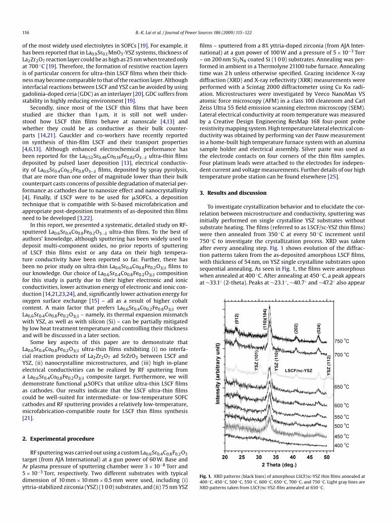
1 wer S
ohLainigs
sswpo[bditcf[tan
sadotbofcdocLwba
LcYeadaccm[
2
tA5dy
fin–ftdpaaZLbrdistFdt
3
risw7atwith thickness of 54 nm, on YSZ single crystalline substrates uponsequential annealing. As seen in Fig. 1, the films were amorphouswhen annealed at 400 ◦C. After annealing at 450 ◦C, a peak appearsat ∼33.1◦ (2-theta). Peaks at ∼23.1◦, ∼40.7◦ and ∼47.2◦ also appear
16 B.-K. Lai et al. / Journal of Po
f the most widely used electrolytes in SOFCs [19]. For example, itas been reported that in La0.9Sr0.1MnO3-YSZ systems, thickness ofa2Zr2O7 reaction layer could be as high as 25 nm when treated onlyt 700 ◦C [19]. Therefore, the formation of resistive reaction layerss of particular concern for ultra-thin LSCF films when their thick-ess may become comparable to that of the reaction layer. Although
nterfacial reactions between LSCF and YSZ can be avoided by usingadolinia-doped ceria (GDC) as an interlayer [20], GDC suffers fromtability in highly reducing environment [19].
Secondly, since most of the LSCF thin films that have beentudied are thicker than 1 �m, it is still not well under-tood how LSCF thin films behave at nanoscale [4,13] andhether they could be as conductive as their bulk counter-arts [14,21]. Gauckler and co-workers have recently reportedn synthesis of thin-film LSCF and their transport properties4,6,13]. Although enhanced electrochemical performance haseen reported for the La0.52Sr0.48Co0.18Fe0.82O3−ı ultra-thin filmseposited by pulsed laser deposition [13], electrical conductiv-
ty of La0.6Sr0.4Co0.2Fe0.8O3−ı films, deposited by spray pyrolysis,hat are more than one order of magnitude lower than their bulkounterpart casts concerns of possible degradation of material per-ormance as cathodes due to nanosize effect and nanocrystallinity4]. Finally, if LSCF were to be used for �SOFCs, a depositionechnique that is compatible with Si-based microfabrication andppropriate post-deposition treatments of as-deposited thin filmseed to be developed [3,22].
In this report, we presented a systematic, detailed study on RF-puttered La0.6Sr0.4Co0.8Fe0.2O3−ı ultra-thin films. To the best ofuthors’ knowledge, although sputtering has been widely used toeposit multi-component oxides, no prior reports of sputteringf LSCF thin films exist or any data on their high tempera-ure conductivity have been reported so far. Further, there haseen no prior study on ultra-thin La0.6Sr0.4Co0.8Fe0.2O3(ı films tour knowledge. Our choice of La0.6Sr0.4Co0.8Fe0.2O3(ı compositionor this study is partly due to their higher electronic and ioniconductivities, lower activation energy of electronic and ionic con-uction [14,21,23,24], and, significantly lower activation energy forxygen surface exchange [15] – all as a result of higher cobaltontent. A main factor that prefers La0.6Sr0.4Co0.2Fe0.8O3(ı overa0.6Sr0.4Co0.8Fe0.2O3(ı – namely, its thermal expansion mismatchith YSZ, as well as with silicon (Si) – can be partially mitigated
y low heat treatment temperature and controlling their thicknessnd will be discussed in a later section.
Some key aspects of this paper are to demonstrate thata0.6Sr0.4Co0.8Fe0.2O3(ı ultra-thin films exhibiting (i) no interfa-ial reaction products of La2Zr2O7 ad SrZrO3 between LSCF andSZ, (ii) nanocrystalline microstructures, and (iii) high in-planelectrical conductivities can be realized by RF sputtering fromLa0.6Sr0.4Co0.8Fe0.2O3(ı composite target. Furthermore, we will
emonstrate functional �SOFCs that utilize ultra-thin LSCF filmss cathodes. Our results indicate that the LSCF ultra-thin filmsould be well-suited for intermediate- or low-temperature SOFCathodes and RF sputtering provides a relatively low-temperature,icrofabrication-compatible route for LSCF thin films synthesis
21].
. Experimental procedure
RF sputtering was carried out using a custom La0.6Sr0.4C0.8F0.2O3
arget (from AJA International) at a gun power of 60 W. Base andr plasma pressure of sputtering chamber were 3 × 10⁻⁸ Torr and× 10−3 Torr, respectively. Two different substrates with typicalimension of 10 mm × 10 mm × 0.5 mm were used, including (i)ttria-stabilized zirconia (YSZ) (1 0 0) substrates, and (ii) 75 nm YSZF4X
ources 186 (2009) 115–122
lms – sputtered from a 8% yttria-doped zirconia (from AJA Inter-ational) at a gun power of 100 W and a pressure of 5 × 10⁻³ Torron 200 nm Si3N4 coated Si (1 0 0) substrates. Annealing was per-
ormed in ambient in a Thermolyne 21100 tube furnace. Annealingime was 2 h unless otherwise specified. Grazing incidence X-rayiffraction (XRD) and X-ray reflectivity (XRR) measurements wereerformed with a Scintag 2000 diffractometer using Cu K� radi-tion. Microstructures were investigated by Veeco NanoMan VStomic force microscopy (AFM) in a class 100 cleanroom and Carleiss Ultra 55 field emission scanning electron microscopy (SEM).ateral electrical conductivity at room temperature was measuredy a Creative Design Engineering ResMap 168 four-point probeesistivity mapping system. High temperature lateral electrical con-uctivity was obtained by performing van der Pauw measurement
n a home-built high temperature furnace system with an aluminaample holder and electrical assembly. Silver paste was used ashe electrode contacts on four corners of the thin film samples.our platinum leads were attached to the electrodes for indepen-ent current and voltage measurements. Further details of our highemperature probe station can be found elsewhere [25].
. Results and discussion
To investigate crystallization behavior and to elucidate the cor-elation between microstructure and conductivity, sputtering wasnitially performed on single crystalline YSZ substrates withoutubstrate heating. The films (referred to as LSCF/sc-YSZ thin films)ere then annealed from 350 ◦C at every 50 ◦C increment until50 ◦C to investigate the crystallization process. XRD was takenfter every annealing step. Fig. 1 shows evolution of the diffrac-ion patterns taken from the as-deposited amorphous LSCF films,
ig. 1. XRD patterns (black lines) of amorphous LSCF/sc-YSZ thin films annealed at00 ◦C, 450 ◦C, 500 ◦C, 550 ◦C, 600 ◦C, 650 ◦C, 700 ◦C, and 750 ◦C. Light gray lines areRD patterns taken from LSCF/nc-YSZ-film annealed at 650 ◦C.
B.-K. Lai et al. / Journal of Power S
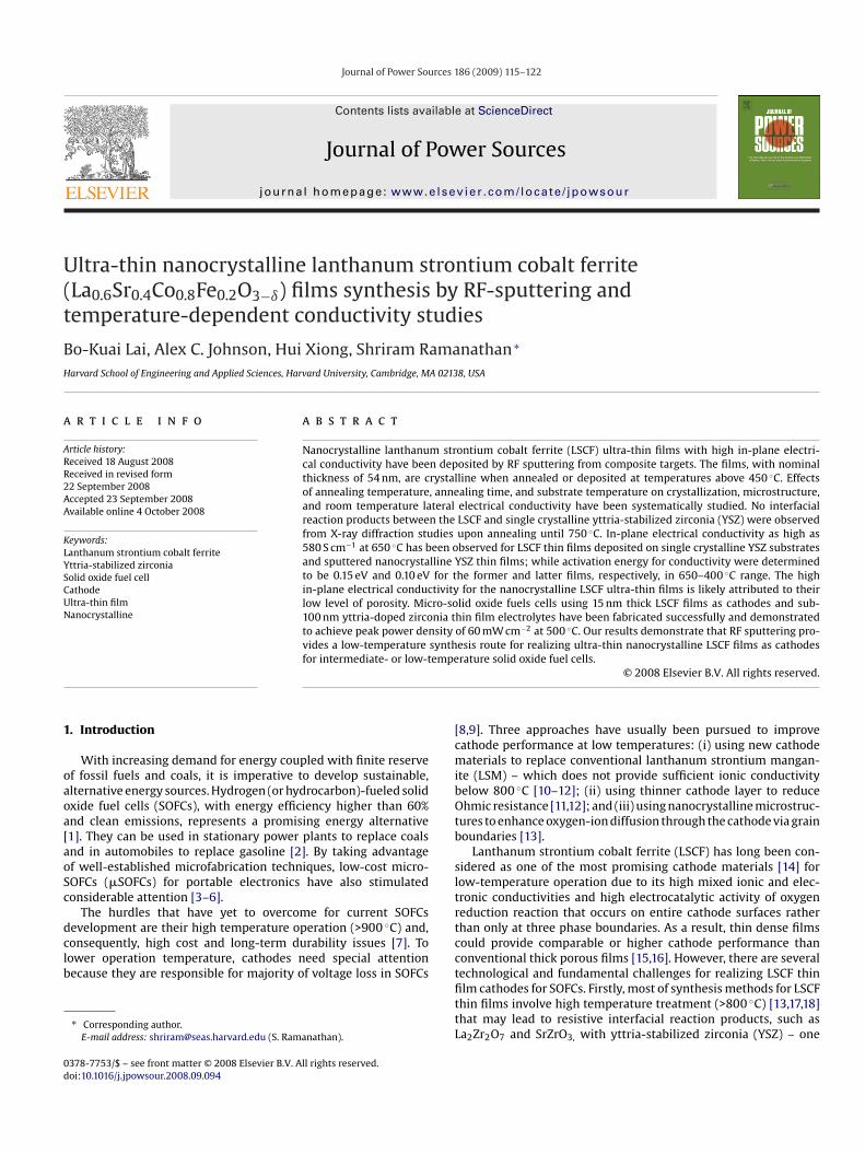
Fig. 2. RT conductivity of amorphous LSCF/sc-YSZ thin films annealed sequentially(square symbols) at 400 ◦C, 450 ◦C, 550 ◦C, and 750 ◦C. Circular and triangular sym-bols represent LSCF/sc-YSZ thin films annealed directly at 500 ◦C for 2 h and 20 h,rga
ai(s
ptXAsfiaY∼
paaTic(iSrwoteLtlarger grains, hence less grain boundaries, RT conductivity of 750 ◦C
espectively. Inset on the upper right displays electrical conductivity as a function ofrain diameter, whose range is indicated by error bars, for 450 ◦C, 500 ◦C, and 550 ◦Cnnealed LSCF/sc-YSZ thin films.
t 450 ◦C and they become more discernible at higher anneal-ng temperatures. Compared to rhombohedral La0.6Sr0.4C0.8F0.2O3JCPDS 48-0124 [26]), the 33.1◦ peak is identified as the superpo-ition of (1 1 0) and (1 0 4) peaks, while the 23.1◦, 40.7◦ and 47.2◦
al
t
Fig. 3. AFM images taken from LSCF/sc-YSZ thin films annea
ources 186 (2009) 115–122 117
eaks represent (1 0 0), (2 0 2) and (0 2 4) peaks, respectively. Notehat relative intensity of the peaks is in agreement with reported-ray data for LSCF bulk crystals with identical composition [27].s seen in Fig. 1, these four characteristic LSCF peaks can be clearlyeen in 650 ◦C annealed 54 nm LSCF films on nanocrystalline YSZlms that were deposited on Si3N4-coated Si substrates (referred tos LSCF/nc-YSZ thin films). Note that for the LSCF/nc-YSZ thin films,SZ (1 0 1) peak at ∼30.0◦, (110) peak at ∼35.0◦, and (1 1 2) peak at50.5◦ (JCPDS 30-1468 [28]) are also visible.
Fig. 2 shows RT conductivity as a function of annealing tem-erature for the films annealed at 400 ◦C, 450 ◦C, 500 ◦C, 550 ◦C,nd 750 ◦C – note that circular and triangular symbols are fornnealing time study at 500 ◦C, and is discussed further below.he crystallization is also evident from the significant increasen room temperature (RT) lateral electrical conductivity (�) whenomparing 450 ◦C annealed (� = 151.35 S cm−1) to 400 ◦C annealed� = 0.03 S cm−1) LSCF/sc-YSZ thin films. The maximum conductiv-ty (� = 242.24 S cm−1) was found for the films annealed at 550 ◦C.uch high RT electrical conductivity is extremely close to the valueeported (� ∼ 267 S cm−1) in Ref. [23] for macrocrystalline LSCFith the same composition. Electrical conductivity as a function
f grain size is shown in the inset of Fig. 2. The result clearly showshat despite affected by nanoscale grains and their boundaries,lectrical conductivity is still reasonably high in nanocrystallineSCF thin films. Although even higher conductivity is expected forhe films that were annealed at higher temperatures due to their
nnealed thin films (� = 19.12 S cm−1) is one order of magnitudeower compared to the 550 ◦C annealed thin films.
To have a better microscopic insight of the annealing-emperature-dependent of conductivity, microstructure evolution
led at (a) 350 ◦C, (b) 450 ◦C, (c) 550 ◦C, and (d) 750 ◦C.
118 B.-K. Lai et al. / Journal of Power S
Fa
ofYrsoTuscinaiisSbatfitbl
hci7
tY5tfio1TtcXgwr
twfi4dt0fisriiFeipahtCil
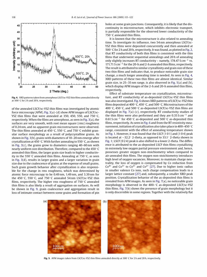
ig. 4. XRD patterns taken from amorphous LSCF/sc-YSZ thin films annealed directlyt 500 ◦C for 2 h and 20 h, respectively.
f the annealed LSCF/sc-YSZ thin films was investigated by atomicorce microscopy (AFM). Fig. 3(a)–(d) show AFM images of LSCF/sc-SZ thin films that were annealed at 350, 450, 550, and 750 ◦C,espectively. When the films are amorphous, as seen in Fig. 3(a), theurfaces are very smooth, with root mean square (rms) roughnessf 0.24 nm, and no apparent grain microstructures were observed.he thin films annealed at 450 ◦C, 550 ◦C, and 750 ◦C exhibit gran-lar surface morphology as a result of polycrystalline grains. Ashown in Fig. 3(b), grains with diameters of 10–20 nm emerge afterrystallization at 450 ◦C. With further annealing to 550 ◦C, as shownn Fig. 3(c), the grains grow to diameters ranging 40–60 nm withearly uniform size distribution. Therefore, compared to the 450 ◦Cnnealed thin films, the larger grain size leads to higher conductiv-ty in the 550 ◦C annealed thin films. Annealing at 750 ◦C, as seenn Fig. 3(d), results in larger grains and a larger variation in grainize due to the coalescence of grains at the expense of small grains.uch grain growth behavior after crystallization is also responsi-le for the change in rms roughness, which was determined bytomic force microscopy to be 0.49 nm, 1.49 nm, and 3.39 nm for
◦ ◦ ◦
he 450 C, 550 C, and 750 C annealed 54 nm LSCF/sc-YSZ thinlms, respectively. The higher rms roughness of 750 ◦C annealedhin films is also likely a result of aggregation on surfaces. As wille shown in Fig. 9, grain coalescence and aggregation result inoss of intimate contact between some grains and formation of pin
prmti
Fig. 5. AFM images taken from LSCF/sc-YSZ thin films anne
ources 186 (2009) 115–122
oles at some grain junctions. Consequently, it is likely that the dis-ontinuity in microstructure, which inhibits electronic transport,s partially responsible for the observed lower conductivity of the50 ◦C annealed thin films.
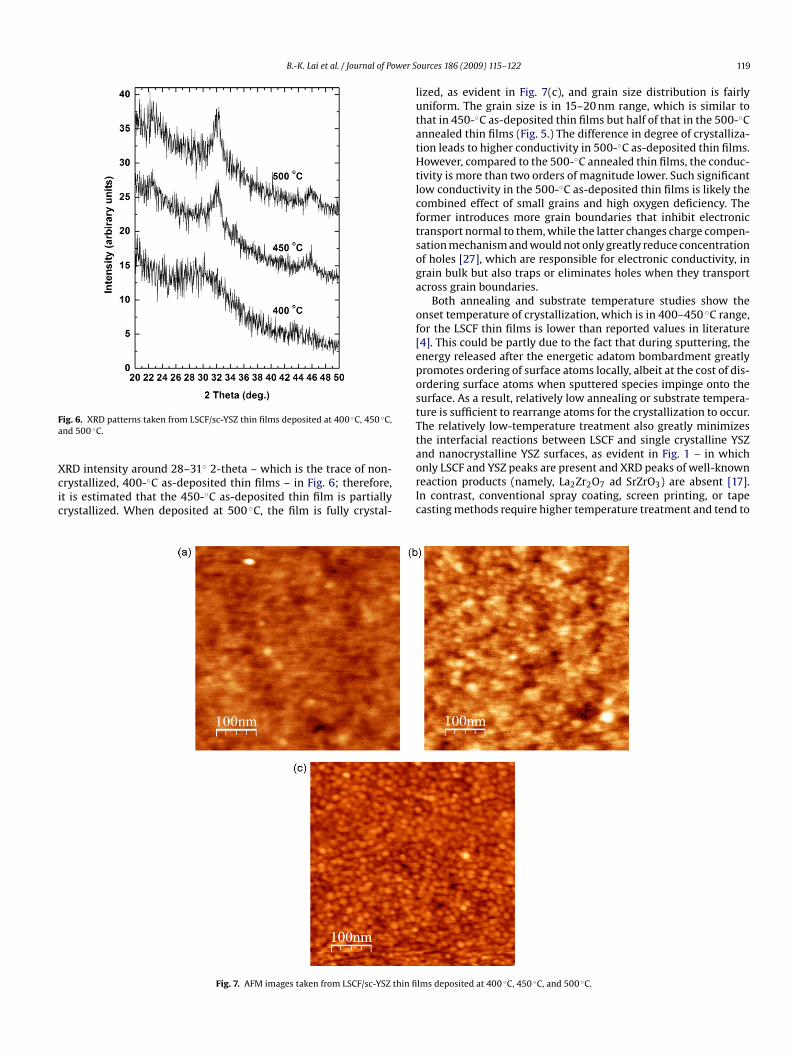
It is known that the microstructure is also related to annealingime. To investigate its influence, two 54 nm amorphous LSCF/sc-SZ thin films were deposited concurrently and then annealed at00 ◦C for 2 h and 20 h, respectively. It was found, as plotted in Fig. 2,hat RT conductivity of both thin films is consistent with the thinlms that underwent sequential annealings and 20 h of annealingnly slightly increases RT conductivity – namely, 178.47 S cm−1 vs.71.71 S cm−1 for the 20-h and 2-h annealed thin films, respectively.he result is attributed to similar crystallinity and grain size of thesewo thin films and indicates that, to produce noticeable grain sizehange, a much longer annealing time is needed. As seen in Fig. 4,RD patterns of these two thin films are almost identical. Similarrain size, in 25–35 nm range, is also observed in Fig. 5(a) and (b),hich display AFM images of the 2-h and 20-h annealed thin films,
espectively.Effect of substrate temperature on crystallization, microstruc-
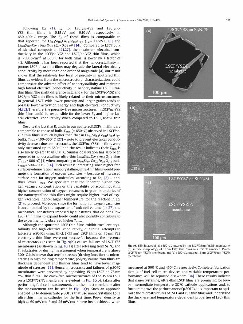
ure, and RT conductivity of as-deposited LSCF/sc-YSZ thin filmsas also investigated. Fig. 6 shows XRD patterns of LSCF/sc-YSZ thinlms deposited at 400 ◦C, 450 ◦C, and 500 ◦C. Microstructures of the00 ◦C, 450 ◦C, and 500 ◦C as-deposited LSCF/sc-YSZ thin films areisplayed in Fig. 7(a)–(c), respectively. RT conductivity studies ofhe thin films were also performed and they are 0.35 S cm−1 and.61 S cm−1 for 450 ◦C as-deposited and 500 ◦C as-deposited thinlms, respectively. As seen in Fig. 6 and from the RT resistivity mea-urement, initiation of crystallization also takes place in 400–450 ◦Cange, consistent with the effect of annealing temperature shownn Fig. 1. However, it was found that the LSCF (1 0 1) and (1 0 4) peaks located at ∼32.2◦ 2-theta, as opposed to 33.1◦ 2-theta shown inig. 1; LSCF (0 2 4) peak is also shifted to a lower 2-theta. The differ-nce is attributed to the as-deposited LSCF thin films crystallizingn extremely low oxygen partial pressure environment and, hence,ossesses greater oxygen non-stoichiometry when compared toir-annealed thin films. The oxygen non-stoichiometry introducesigh level of oxygen vacancies. Moreover, to maintain charge neu-rality, the loss of oxygen is compensated by Co reduction fromo4+ and Co3+ to Co3+ and Co2+ [27]. Due to higher ionic radius
n smaller valence Co ions, such charge compensation leads to aarger lattice constant [27] and, subsequently, a smaller XRD peak
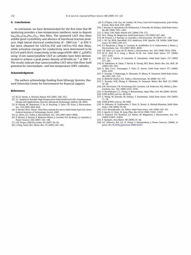
osition. Crystallization behavior of the as-deposited thin films isevealed from AFM images. As seen in Fig. 7(a), no noticeable grainorphology is observed in the 400-◦C as-deposited LSCF/sc-YSZhin films. Fig. 7(b) shows the presence of grain morphology but its only discernible in some regions. Together with the relatively flat
aled directly at 500 ◦C for 2 h and 20 h, respectively.
B.-K. Lai et al. / Journal of Power S
Fa
Xcic
lutatHtlcftsoga
of[epostTtand nanocrystalline YSZ surfaces, as evident in Fig. 1 – in which
ig. 6. XRD patterns taken from LSCF/sc-YSZ thin films deposited at 400 ◦C, 450 ◦C,nd 500 ◦C.
RD intensity around 28–31◦ 2-theta – which is the trace of non-rystallized, 400-◦C as-deposited thin films – in Fig. 6; therefore,t is estimated that the 450-◦C as-deposited thin film is partiallyrystallized. When deposited at 500 ◦C, the film is fully crystal-
orIc
Fig. 7. AFM images taken from LSCF/sc-YSZ thin fi
ources 186 (2009) 115–122 119
ized, as evident in Fig. 7(c), and grain size distribution is fairlyniform. The grain size is in 15–20 nm range, which is similar tohat in 450-◦C as-deposited thin films but half of that in the 500-◦Cnnealed thin films (Fig. 5.) The difference in degree of crystalliza-ion leads to higher conductivity in 500-◦C as-deposited thin films.owever, compared to the 500-◦C annealed thin films, the conduc-
ivity is more than two orders of magnitude lower. Such significantow conductivity in the 500-◦C as-deposited thin films is likely theombined effect of small grains and high oxygen deficiency. Theormer introduces more grain boundaries that inhibit electronicransport normal to them, while the latter changes charge compen-ation mechanism and would not only greatly reduce concentrationf holes [27], which are responsible for electronic conductivity, inrain bulk but also traps or eliminates holes when they transportcross grain boundaries.
Both annealing and substrate temperature studies show thenset temperature of crystallization, which is in 400–450 ◦C range,or the LSCF thin films is lower than reported values in literature4]. This could be partly due to the fact that during sputtering, thenergy released after the energetic adatom bombardment greatlyromotes ordering of surface atoms locally, albeit at the cost of dis-rdering surface atoms when sputtered species impinge onto theurface. As a result, relatively low annealing or substrate tempera-ure is sufficient to rearrange atoms for the crystallization to occur.he relatively low-temperature treatment also greatly minimizeshe interfacial reactions between LSCF and single crystalline YSZ
nly LSCF and YSZ peaks are present and XRD peaks of well-knowneaction products (namely, La2Zr2O7 ad SrZrO3) are absent [17].n contrast, conventional spray coating, screen printing, or tapeasting methods require higher temperature treatment and tend to
lms deposited at 400 ◦C, 450 ◦C, and 500 ◦C.

120 B.-K. Lai et al. / Journal of Power S
Fig. 8. Arrhenius plot of product of in-plane electrical conductivity and tempera-tso
fait
cptt(t75thlmtFm
ac
fiiCfoomcntt(do
etL[ntfp(oSe
ils
�
wavfv
·· x ·· x 1
Fi
ure for LSCF/sc-YSZ (�) and LSCF/nc-YSZ (�) thin films. The corresponding layertructure and symbol for each film are illustrated on the bottom of the figure. Insetn the upper right is an XRR pattern taken from LSCF/sc-YSZ thin films.
orm reaction layers with thicknesses of tens of nm between LSCFnd YSZ [17,19]. Although a ceria interlayer can be used to avoidnterfacial reactions, it suffers from stability under low oxygen par-ial pressures [19].
Fig. 8 shows an Arrhenius plot of product of lateral electricalonductivity, �, and temperature, T, as function of reciprocal tem-erature for the LSCF/sc-YSZ and LSCF/nc-YSZ thin films. Depositionime is the same for both LSCF thin films and quantitative analysis ofhe X-ray reflectivity pattern taken from the LSCF/sc-YSZ thin filmsdisplayed as an inset) indicates their film thickness is∼54 nm. Prioro the measurement, the LSCF/sc-YSZ thin films were annealed at50 ◦C, while LSCF/nc-YSZ thin films were annealed at 650 ◦C forh to stabilize the microstructures. Note that since YSZ single crys-
al is not an electronic conductor under the conditions reportedere and has ionic conductivity nearly three orders of magnitude
ower [1] than the measured lateral electrical conductivity, the
easured lateral electrical conductivity should primarily representhe total electronic and ionic conductivity of the LSCF thin films.urthermore, since electronic conductivity of LSCF is three orders oragnitude higher than its ionic conductivity [14], it is reasonable to
2
Afn
ig. 9. SEM images of (a) LSCF/sc-YSZ and (b) LSCF/nc-YSZ thin films after high temperndicated by an arrow on the lower left.
ources 186 (2009) 115–122
ssume that the measured lateral electrical conductivity representsontribution from LSCF and its adjacent surfaces/interfaces.
After the measurement, surface morphologies of the samelms were investigated by SEM. Figs. 9(a) and 4(b) show the SEM
mages of LSCF/sc-YSZ and LSCF/nc-YSZ thin films, respectively.ompared to Fig. 3(d) – for which the films were annealed at 750 ◦C
or 2 h, crystallites larger than 100 nm are formed on the surfacef LSCF/sc-YSZ thin films. It is likely due to further coalescencef grains during the additional annealing time (5 h) prior to theeasurement. As seen in Fig. 9(a), LSCF/sc-YSZ thin films are
rack-free. However, some of the grains and grain junctions areot in intimate contact. In contrast, the grains in the LSCF/nc-YSZhin films are all in close contact. However, due to the largehermal expansion mismatch between La0.6Sr0.4Co0.8Fe0.2O3(ı
= ∼21.2 × 10⁻⁶ K−1) [29] and Si (= ∼3 × 10⁻⁶ K−1), microcracksevelop after the 650 ◦C treatment. Note that such microcracks arenly visible in high-resolution SEM images.
As seen in Fig. 8, the temperature dependence of in-planelectrical conductivity in LSCF/sc-YSZ thin films is similar tohat of LSCF bulk with the same [27] and similar (namely,a0.8Sr0.2Co0.8Fe0.2O3(ı in Ref. [14], La0.4Sr0.6Co0.8Fe0.2O3(ı in Ref.18], and La0.6Sr0.4Co0.2Fe0.8O3(ı in Ref. [30]) compositions –amely, lateral electrical conductivity increases with increasingemperature, reaches a maximum, and then decreases with aurther increase in temperature. Such behavior is due to the com-etition between oxygen vacancy (VO
••) charge and hole carrierBB
•) compensation mechanism in LSCF, which possesses ABO3 per-vskite structures. The hole carrier BB
• in LSCF is a result of divalentr dopants in trivalent La occupied A sites and lower polaron sitenergy in B-site cations [14,18].
Below the temperature at which maximum conductivity occurs,.e., T < Tmax, hole carrier compensation mechanism dominates andateral electrical conductivity is attributed to thermal activation ofmall polaron hopping [4,14,18] that is generally expressed by [31]
=(
�0
T
)exp
(−Ea
kBT
), (1)
here �0 is conductivity coefficient, kB is Boltzmann’s constant,nd Ea is the activation energy [30]. When T is above Tmax, oxygenacancy (VO
••) charge compensation mechanism prevails due to theormation of oxygen vacancies [14]. As seen in Eq. (2), each oxygenacancy creation leads to consumption of two hole carriers.
BB + OO → VO + 2BB + 2 O2 (2)
s a result, when T > Tmax, lateral electrical conductivity that arisesrom thermally activated polarons decreases rapidly. Such phe-omenon is well known in LSCF bulk crystals [14,18,27].
ature electrical conductivity measurement. A representative microcrack in (b) is
wer Sources 186 (2009) 115–122 121
Y6tLodi∼pcsfichtLIp[tefi
cYbtoar(Tsmstghtg(imLt
tfeomS3ctnmYopteuh
Fig. 10. SEM images of (a) a 650 ◦C annealed 54 nm-LSCF/75 nm-YSZ/Pt membrane,(Lm
mdft
B.-K. Lai et al. / Journal of Po
Following Eq. (1), Ea for LSCF/sc-YSZ and LSCF/nc-SZ thin films is 0.15 eV and 0.10 eV, respectively, in50–400 ◦C range. The Ea of these films is comparable tohat reported for La0.4Sr0.6Co0.8Fe0.2O3(ı (Ea = 0.17 eV) [18] anda0.8Sr0.2Co0.8Fe0.2O3(ı (Ea = 0.08 eV [14].) Compared to LSCF bulkf identical composition [21,27], the maximum electrical con-uctivity in the LSCF/sc-YSZ and LSCF/nc-YSZ thin films, which
s ∼580 S cm−1 at 650 ◦C for both films, is lower by a factor of2. Although it has been reported that the nanocrystallinity inorous LSCF ultra-thin films may degrade the lateral electricallyonductivity by more than one order of magnitude [4], our resulthows that the relatively low level of porosity in sputtered thinlms as evident from the microstructural characterization, couldompensate the adverse effect of nanocrystallinity and maintainigh lateral electrical conductivity in nanocrystalline LSCF ultra-hin films. The slight difference in Ea and � for the LSCF/sc-YSZ andSCF/nc-YSZ thin films is likely related to their microstructures.n general, LSCF with lower porosity and larger grains tends toossess lower activation energy and high electrical conductivity4,32]. Therefore, the porosity-free microstructures in LSCF/nc-YSZhin films could be responsible for the lower Ea and higher lat-ral electrical conductivity when compared to LSCF/sc-YSZ thinlms.
Despite the fact that Ea and � in our sputtered LSCF thin films areomparable to those of bulk, Tmax (= 650 ◦C) observed in LSCF/sc-SZ thin films is much higher than that in La0.6Sr0.4Co0.8Fe0.2O3(ıulks, Tmax = 100–350 ◦C [27] – note to prevent electrical conduc-ivity decrease due to microcracks, the LSCF/nc-YSZ thin films werenly measured up to 650 ◦C and the result indicates their Tmax islso likely greater than 650 ◦C. Similar observation has also beeneported in nanocrystalline, ultra-thin La0.6Sr0.4Co0.2Fe0.8O3(ı filmsTmax > 800 ◦C) [4] when comparing to La0.6Sr0.4Co0.2Fe0.8O3(ı bulk,max = 500–700 ◦C [14]. Such result is interesting since higher freeurface/volume ratio in nanocrystalline, ultra-thin films would pro-ote the formation of oxygen vacancies – because of increased
urface area for oxygen molecules, according to Eq. (2) – and,hus, lower Tmax. We speculate that the inherent higher oxy-en vacancy concentration or the capability of accommodatingigher concentration of oxygen vacancies in grain boundaries ofhe nanocrystalline thin films might require higher level of oxy-en vacancies, hence, higher temperature, for the reaction in Eq.2) to proceed. Moreover, since the formation of oxygen vacanciess accompanied by the expansion of unit cell volume [14,27], the
echanical constraints imposed by substrates, that do not allowSCF thin films to expand freely, could also possibly contribute tohe experimentally observed higher Tmax.
Although the sputtered LSCF thin films exhibit excellent crys-allinity and high electrical conductivity, our initial attempts toabricate �SOFCs using thick (>55 nm) LSCF films on 75 nm YSZlectrolyte thin films were not successful because the presencef microcracks (as seen in Fig. 9(b)) causes failures of LSCF-YSZembranes (as shown in Fig. 10(a)) after releasing from Si3N4 and
i substrates or during measurement when temperature is above00 ◦C. It is known that tensile stresses (driving force for the micro-racks) in high melting temperature, polycrystalline thin films arehickness dependent and thinner films tend to have lower mag-itude of stresses [33]. Hence, microcracks and failures of �SOFCembranes were prevented by depositing 15 nm LSCF on 75 nm
SZ thin films. The crack-free microstructures of the 15 nm LSCFn a LSCF/YSZ/Pt membrane is evident in Fig. 10(b), taken after
erforming fuel cell measurement, and the intact membrane afterhe measurement can be seen in Fig. 10(c). Such an approachnabled us to demonstrate �SOFCs that use nanocrystalline LSCFltra-thin films as cathodes for the first time. Power density asigh as 60 mW cm−2 and 25 mW cm−2 have been achieved whenofmtfi
b) surface morphology of 15 nm LSCF thin films in a 650 ◦C annealed 15 nm-SCF/75 nm-YSZ/Pt membrane, and (c) a 650 ◦C annealed 15 nm-LSCF/75 nm-YSZ/Ptembrane.
easured at 500 ◦C and 450 ◦C, respectively. Complete fabricationetails of fuel cell micro-devices and variable temperature per-ormance will be reported elsewhere [34]. These results indicatehat nanocrystalline, ultra-thin LSCF films are promising for low-r intermediate-temperature SOFC cathode applications and, to
urther improve the performance of �SOFCs, it is important to opti-ize the microstructures of LSCF and YSZ thin films and understandhe thickness- and temperature-dependent properties of LSCF thinlms.
1 wer S
4
sLeuhw0usTp
A
v
R
[
[[[[
[
[[
[
[
[
[
[[
[
[[[
[[
[
22 B.-K. Lai et al. / Journal of Po
. Conclusions
In conclusion, we have demonstrated for the first time that RFputtering provides a low-temperature synthesis route to deposita0.6Sr0.4Co0.8Fe0.2O3(ı thin films. The sputtered LSCF thin filmsxhibit good crystallinity and absence of interfacial reaction prod-cts. High lateral electrical conductivity of ∼580 S cm−1 at 650 ◦Cas been obtained for LSCF/nc-YSZ and LSCF/sc-YSZ thin films;hile activation energies for conductivity were determined to be
.15 eV and 0.10 eV, respectively, in the range of 650–400 ◦C. �SOFCssing 15 nm nanocrystalline LSCF as cathodes have been demon-trated to achieve a peak power density of 60 mW cm−2 at 500 ◦C.he results indicate that nanocrystalline LSCF ultra-thin films holdotential for intermediate- and low-temperature SOFC cathodes.
cknowledgment
The authors acknowledge funding from SiEnergy Systems, Har-ard University Center for Environment for financial support.
eferences
[1] B.C.H. Steele, A. Heinzel, Nature 414 (2001) 345–352.[2] S.C. Singhal, K. Kendall, High Temperature Solid Oxide Fuel Cells: Fundamentals,
Design and Applications, Elsevier Advanced Technology, Oxford, UK, 2003.[3] H. Huang, M. Nakamura, P. Su, R. Fasching, Y. Saito, F.B. Prinz, J. Electrochem.
Soc. 154 (2007) B20–B24.[4] D. Beckel, Ph.D. Thesis, Thin Film Cathode for micro Solid Oxide Fuel Cell, Swiss
Federal Institute of Technology, Zurich, 2007.[5] J.L. Hertz, H.L. Tuller, J. Electrochem. Soc. 154 (2007) B413–B418.[6] D. Beckel, D. Briand, A. Bieberle-Hütter, J. Courbat, N.F. de Rooij, L.J. Gauckler, J.
Power Sources 166 (2007) 143–148.[7] J.W. Fergus, JOM December 59 (2007) 56–62.[8] J. Fleig, Annu. Rev. Mater. Res. 33 (2003) 361–382.
[[
[[
ources 186 (2009) 115–122
[9] R. O’Hayre, S.W. Cha, W. Colella, F.B. Prinz, Fuel Cell Fundamentals, John Wiley& Sons, New York, USA, 2005.
10] I. Yasuda, K. Ogasawara, M. Hishinuma, T. Kawada, M. Dokiya, Solid State Ionics86–88 (1996) 1197–1201.
11] Z. Shao, S.M. Haile, Nature 431 (2004) 170–173.12] W.G. Wang, M. Mogensen, Solid State Ionics 176 (2005) 457–462.13] M. Prestat, J.-F. Koenig, L.J. Gauckler, J. Electroceram. 18 (2007) 111–120.14] L.-W. Tai, M.M. Nasrallah, H.U. Anderson, D.M. Sparlin, S.R. Sehlin, Solid State
Ionics 76 (1995) 259–271.15] F.S. Baumann, J. Fleig, G. Cristiani, B. Stuhlhofer, H.-U. Habermeier, J. Maier, J.
Electrochem. Soc. 154 (2007) B931–B941.16] S.B. Adler, J.A. Lane, B.C.H. Steele, J. Electrochem. Soc. 143 (1996) 3554–3564.17] W.-H. Kim, H.-S. Song, J. Moon, H.-W. Lee, Solid State Ionics 177 (2006)
3211–3216.18] H.Y. Tu, Y. Takeda, N. Imanishi, O. Yamamoto, Solid State Ionics 117 (1999)
277–281.19] H. Yokokawa, N. Sakai, T. Horita, K. Yamaji, M.E. Brito, Mater. Res. Soc. Bull. 30
(2005) 591–595.20] A. Mai, V.A.C. Haanappel, F. Tietz, D. Stover, Solid State Ionics 177 (2006)
2103–2107.21] Y. Teraoka, T. Nobunaga, K. Okamoto, N. Miura, N. Yamazoe, Solid State Ionics
48 (1991) 207–212.22] A. Bieberle-Hutter, H.L. Tuller, J. Electroceram. 16 (2006) 151–157.23] Y. Teraoka, H.M. Zhang, K. Okamoto, N. Yamazoe, Mater. Res. Bull. 23 (1988)
51–58.24] J.W. Stevenson, T.R. Armstrong, R.D. Carneim, L.R. Pederson, W.J. Weber, J. Elec-
trochem. Soc. 143 (1996) 2722–2729.25] A. Karthikeyan, C.L. Chang, S. Ramanathan, Appl. Phys. Lett. 89 (2006) 183116.26] ICDD-JCPDS card no. 48-0124.27] S. Wang, M. Katsuki, M. Dokiya, T. Hashimoto, Solid State Ionics 159 (2003)
71–78.28] ICDD-JCPDS card no. 30-1468.29] H. Ullmann, N. Trofimenko, F. Tietz, D. Stover, A. Ahmad-Khanlou, Solid State
Ionics 138 (2000) 79–90.30] G.Ch. Kostogloudis, Ch. Ftikos, Solid State Ionics 126 (1999) 143–151.
31] E. Iguchi, K. Ueda, W. Jung, Phys. Rev. B 54 (1996) 17431–17437.32] A. Esquirol, N.P. Brandon, J.A. Kilner, M. Mogensen, J. Electrochem. Soc. 151(2004) A1847–A1855.33] F. Spaepen, Acta Mater. 48 (2000) 31–42.34] A.C. Johnson, B.K. Lai, H. Xiong, S. Ramanathan, J. Power Sources, (2008), in
press, doi:10.1016/j.jpowsour.2008.10.021.