
An experimental investigation into micro-fabricated solid oxide fuel cells with ultra-thin La 0.6Sr...
9
Journal of Power Sources 186 (2009) 252–260 Contents lists available at ScienceDirect Journal of Power Sources journal homepage: www.elsevier.com/locate/jpowsour An experimental investigation into micro-fabricated solid oxide fuel cells with ultra-thin La 0.6 Sr 0.4 Co 0.8 Fe 0.2 O 3 cathodes and yttria-doped zirconia electrolyte films Alex C. Johnson ∗ , Bo-Kuai Lai, Hui Xiong, Shriram Ramanathan Harvard School of Engineering and Applied Sciences, Harvard University, Cambridge, MA 02138, United States article info Article history: Received 29 August 2008 Received in revised form 8 October 2008 Accepted 8 October 2008 Available online 17 October 2008 Keywords: Solid oxide fuel cell (SOFC) Lanthanum strontium cobalt iron oxide (LSCF) Cathode Thin film Impedance spectroscopy abstract Thin-film solid oxide fuel cells (SOFCs) were fabricated with both Pt and mixed conducting oxide cathodes using sputtering, lithography, and etching. Each device consists of a 75–150nm thick yttria-stabilized zirconia (YSZ) electrolyte, a 40–80nm porous Pt anode, and a cathode of either 15–150nm dense La 0.6 Sr 0.4 Co 0.8 Fe 0.2 O 3−ı (LSCF) or 130nm porous Pt. Maximum powers produced by the cells are found to increase with temperature with activation energies of 0.94–1.09eV. At 500 ◦ C, power densities of 90 and 60 mW cm −2 are observed with Pt and LSCF cathodes, respectively, although in some conditions LSCF outperforms Pt. Several device types were fabricated to systematically investigate electrical properties of components of these fuel cells. Micro-fabricated YSZ structures contacted on opposite edges by Pt elec- trodes were used to study temperature-dependent in-plane conductivity of YSZ as a function of lateral size and top and bottom interfaces. Si/Si 3 N 4 /Pt and Si/Si 3 N 4 /Au capacitor structures are fabricated and found to explain certain features observed in impedance spectra of in-plane and fuel cell devices containing silicon nitride layers. The results are of relevance to micro-scale energy conversion devices for portable applications. © 2008 Elsevier B.V. All rights reserved. 1. Introduction Fuel cells are attractive for their high efficiency, low emissions, and direct production of electricity, however their application has been limited by high cost, system complexity, and limited duty or cycle life [1]. Significant research in polymer electrolyte membrane fuel cells (PEMFCs) and solid oxide fuel cells (SOFCs) is focused on strategies to operate in an intermediate temperature range, roughly 200–600 ◦ C [2]. PEMFCs typically operate below 100 ◦ C, but higher temperature would increase catalytic activity and impurity resis- tance. SOFCs typically operate above 700 ◦ C, and lower temperature would bring more material flexibility, less corrosive side reactions, quicker thermal cycling, and easier scaling down, and thus may enable SOFCs to power portable electronics or transportation. Energy conversion in a fuel cell involves a variety of processes in tandem. Some, such as electron transport and gas diffusion, vary little with temperature. Others, such as ion transport and oxidation and reduction reactions, are thermally activated and require signif- icant changes to remain effective as temperature is decreased. Ion transport losses in the electrolyte can be reduced by either increas- ∗ Corresponding author. E-mail address: [email protected] (A.C. Johnson). ing conductivity or reducing thickness. Perhaps the most common SOFC electrolyte is yttria-stabilized zirconia (YSZ). While a vari- ety of more conductive electrolyte materials are being investigated [3], the excellent chemical stability of YSZ is prompting efforts to reduce its thickness to the nanoscale [4–6], which may also benefit conductivity [7–12] and surface exchange [5]. In this paper we report on fabrication and measurement of micro-SOFCs with dense thin-film La 0.6 Sr 0.4 Co 0.8 Fe 0.2 O 3−ı (LSCF) cathodes, with performance comparable to their Pt counterparts, as measured from 200 to 600 ◦ C. In addition, we describe vari- ous components of these micro-fuel cell chips, in detail that has not been addressed previously. We isolate the variable temper- ature impedance spectra of the YSZ electrolyte and the silicon nitride insulator, and investigate the structural characteristics of thin-film sputtered LSCF and Pt electrodes. Intermediate tempera- ture YSZ-based SOFCs have previously been made with Pt cathodes [5,13], however Pt degrades quickly at higher temperatures. LSCF and similar materials, such as Ba 1−x Sr x Co 1−y Fe y O 3−ı , have garnered substantial attention as intermediate temperature SOFC cathodes [14–16] and LSCF has recently been incorporated into a thin-film fuel cell [6]. These materials are stable at high temperatures, and have the advantage as mixed conductors that the entire surface participates in catalysis, thus a dense film can be used, although nanostructuring can still decrease resistance by increasing surface 0378-7753/$ – see front matter © 2008 Elsevier B.V. All rights reserved. doi:10.1016/j.jpowsour.2008.10.021
-
Upload
independent -
Category
Documents
-
view
1 -
download
0
Transcript of An experimental investigation into micro-fabricated solid oxide fuel cells with ultra-thin La 0.6Sr...

Awe
AH
a
ARRAA
KSL(CTI
1
abcfs2ttwqe
ilait
0d
Journal of Power Sources 186 (2009) 252–260
Contents lists available at ScienceDirect
Journal of Power Sources
journa l homepage: www.e lsev ier .com/ locate / jpowsour
n experimental investigation into micro-fabricated solid oxide fuel cellsith ultra-thin La0.6Sr0.4Co0.8Fe0.2O3 cathodes and yttria-doped zirconia
lectrolyte films
lex C. Johnson ∗, Bo-Kuai Lai, Hui Xiong, Shriram Ramanathanarvard School of Engineering and Applied Sciences, Harvard University, Cambridge, MA 02138, United States
r t i c l e i n f o
rticle history:eceived 29 August 2008eceived in revised form 8 October 2008ccepted 8 October 2008vailable online 17 October 2008
eywords:olid oxide fuel cell (SOFC)anthanum strontium cobalt iron oxideLSCF)
a b s t r a c t
Thin-film solid oxide fuel cells (SOFCs) were fabricated with both Pt and mixed conducting oxide cathodesusing sputtering, lithography, and etching. Each device consists of a 75–150 nm thick yttria-stabilizedzirconia (YSZ) electrolyte, a 40–80 nm porous Pt anode, and a cathode of either 15–150 nm denseLa0.6Sr0.4Co0.8Fe0.2O3−ı (LSCF) or 130 nm porous Pt. Maximum powers produced by the cells are foundto increase with temperature with activation energies of 0.94–1.09 eV. At 500 ◦C, power densities of 90and 60 mW cm−2 are observed with Pt and LSCF cathodes, respectively, although in some conditions LSCFoutperforms Pt. Several device types were fabricated to systematically investigate electrical properties ofcomponents of these fuel cells. Micro-fabricated YSZ structures contacted on opposite edges by Pt elec-trodes were used to study temperature-dependent in-plane conductivity of YSZ as a function of lateral size
athodehin filmmpedance spectroscopy
and top and bottom interfaces. Si/Si3N4/Pt and Si/Si3N4/Au capacitor structures are fabricated and foundto explain certain features observed in impedance spectra of in-plane and fuel cell devices containingsilicon nitride layers. The results are of relevance to micro-scale energy conversion devices for portable
iSe[rc
mcaonantt
applications.
. Introduction
Fuel cells are attractive for their high efficiency, low emissions,nd direct production of electricity, however their application haseen limited by high cost, system complexity, and limited duty orycle life [1]. Significant research in polymer electrolyte membraneuel cells (PEMFCs) and solid oxide fuel cells (SOFCs) is focused ontrategies to operate in an intermediate temperature range, roughly00–600 ◦C [2]. PEMFCs typically operate below 100 ◦C, but higheremperature would increase catalytic activity and impurity resis-ance. SOFCs typically operate above 700 ◦C, and lower temperatureould bring more material flexibility, less corrosive side reactions,
uicker thermal cycling, and easier scaling down, and thus maynable SOFCs to power portable electronics or transportation.
Energy conversion in a fuel cell involves a variety of processesn tandem. Some, such as electron transport and gas diffusion, vary
ittle with temperature. Others, such as ion transport and oxidationnd reduction reactions, are thermally activated and require signif-cant changes to remain effective as temperature is decreased. Ionransport losses in the electrolyte can be reduced by either increas-∗ Corresponding author.E-mail address: [email protected] (A.C. Johnson).
[as[fhpn
378-7753/$ – see front matter © 2008 Elsevier B.V. All rights reserved.oi:10.1016/j.jpowsour.2008.10.021
© 2008 Elsevier B.V. All rights reserved.
ng conductivity or reducing thickness. Perhaps the most commonOFC electrolyte is yttria-stabilized zirconia (YSZ). While a vari-ty of more conductive electrolyte materials are being investigated3], the excellent chemical stability of YSZ is prompting efforts toeduce its thickness to the nanoscale [4–6], which may also benefitonductivity [7–12] and surface exchange [5].
In this paper we report on fabrication and measurement oficro-SOFCs with dense thin-film La0.6Sr0.4Co0.8Fe0.2O3−ı (LSCF)
athodes, with performance comparable to their Pt counterparts,s measured from 200 to 600 ◦C. In addition, we describe vari-us components of these micro-fuel cell chips, in detail that hasot been addressed previously. We isolate the variable temper-ture impedance spectra of the YSZ electrolyte and the siliconitride insulator, and investigate the structural characteristics ofhin-film sputtered LSCF and Pt electrodes. Intermediate tempera-ure YSZ-based SOFCs have previously been made with Pt cathodes5,13], however Pt degrades quickly at higher temperatures. LSCFnd similar materials, such as Ba1−xSrxCo1−yFeyO3−ı, have garneredubstantial attention as intermediate temperature SOFC cathodes
14–16] and LSCF has recently been incorporated into a thin-filmuel cell [6]. These materials are stable at high temperatures, andave the advantage as mixed conductors that the entire surfacearticipates in catalysis, thus a dense film can be used, althoughanostructuring can still decrease resistance by increasing surface
Power
aap
cRipsfieptshludacRft
2
2
smoaHtt
puawm(K
2
tfomoTtieaswto
sdrat
Ff
A.C. Johnson et al. / Journal of
rea. In addition to being stable at high temperatures, anotherdvantage may be lower cost of ceramic cathode materials com-ared to precious metals such as Pt.
To the best of our knowledge, this is the first report dis-ussing functional thin-film-based solid oxide fuel cells utilizingF-sputtered LSCF cathode thin films. Advantages of this approach
nclude thin-film cathode processing approach compatible withhotolithography and patterning as well as relative simplicity toynthesize a multi-component, highly dense complex oxide thinlm from a single target. Ref. [5] shows that RF sputtered YSZlectrolytes paired with Pt electrodes can make SOFCs with higherformance at low temperatures, achieving higher power densityhan the similar Pt-cathode cells we report here. Ref. [6] describes aimilar structure, including both LSCF and Pt as cathode materials,owever they deposit the oxide electrolytes and cathodes by pulsed
aser deposition (PLD) or spray pyrolysis (SP). Their Pt-cathode cellses an electrolyte made by one PLD layer and one SP layer toecrease gas leakage and achieve a high open circuit voltage (OCV)nd a maximum power nearly identical to that of the Pt-cathodeell we report here. However, the LSCF-cathode cell described inef. [6] uses a single PLD layer for the electrolyte. This cell suffersrom low OCV and, likely for this reason, lower maximum powerhan the LSCF-cathode cells we report in this article.
. Experimental
.1. Measurement apparatus
At the center of our measurement setup is a hollow stainlessteel block, which can be heated to 600 ◦C. One fuel cell chip, whichay contain many individual cells, can be sealed with a gold o-ring
ver a hole in this block. Through the gold o-ring, the steel blocklso serves as the common anode connection. Wet forming gas (5%2, 3% H2O, balance Ar) is fed to the anode on the bottom of the chip
hrough a coil of tubing, which thermalizes the gas and equilibrateshe H2/O2/H2O system. The top is open to air, and micromanipulator
(pC(A
ig. 1. Optical images and schematics of in-plane conductivity chips. All are Si chips, 10 mmrom 20 to 500 �m contacted by porous Pt, may have Si3N4 above or below the YSZ. (b) St
Sources 186 (2009) 252–260 253
robes with Pt-plated tungsten tips contact the cathodes of individ-al cells. In-plane conductivity devices can be measured in the samepparatus, by flowing no hydrogen and contacting each electrodeith its own micromanipulator probe. Electrical measurements areade either with a Solartron 1260/1287 electrochemical test setup
AC and DC), a Stanford Research 810 lock-in amplifier (AC), or aeithley 2400 sourcemeter (DC).
.2. In-plane electrolyte conductivity devices
Fig. 1 shows optical images and schematics of two device geome-ries used to study the conductivity of thin-film YSZ electrolytes,abricated similarly to the fuel cell electrolytes and in the presencef the same supporting and insulating materials. Conductivitieseasured with these devices reflect electrical transport in the plane
f the surface, rather than through this plane as in fuel cell devices.he value of these measurements is that it is substantially easiero isolate the electrolyte contribution in an in-plane device thann a through-plane device because the overall resistance of thelectrolyte is much greater relative to the electrodes. A reason-ble assumption that electrode polarization can be neglected istrongest for the thinnest films with the largest electrode gaps, butas investigated in detail and found to hold for the full range of film
hicknesses and temperatures used here by comparing resistancesf devices with different electrode gaps.
Both types of device shown in Fig. 1 begin with a 10-mm squareilicon chip coated with 1 �m of thermally grown SiO2. For theevices in Fig. 1(a), rectangles of YSZ are patterned by photolithog-aphy, sputtering, and liftoff. For all YSZ and Pt patterning in thisrticle, LOR-3A lift-off resist (Microchem Corp.) and S1813 pho-oresist (Rohm and Haas Co.) are spun onto the chip and baked
170 and 115 ◦C, respectively). The pattern is exposed through ahotomask, and the S1813 is developed in CD-30 (Rohm and Haaso.). The chip is baked again at 140 ◦C, then developed in CD-26Rohm and Haas Co.) to etch through and undercut the LOR-3A.fter sputtering, the pattern is lifted off in warm (∼60 ◦C) Removeracross, coated with approximately 1 �m SiO2. (a) Square YSZ membranes rangingrips of porous Pt on a blanket YSZ film.

254 A.C. Johnson et al. / Journal of Power Sources 186 (2009) 252–260
F chip, cm YP) m
PtdacrottailbacAt(
kfrlgwetaacSdpT
2
tifis
fmeabShdtsfa
2
ce8lwdcattcdmYr
twwi
ig. 2. Fuel cell structure. (a) Schematic of a cell. (b) Optical image of one 10-mmicrograph of a Pt–YSZ–Pt (PYP) membrane. (d) Cross section of an LSCF–YSZ–Pt (L
G (Microchem Corp.). Because photoresist is present during sput-ering, this technique restricts the substrate to room temperatureuring deposition, although in some cases we annealed the YSZ inir at 800 ◦C for 2 h after liftoff but before Pt deposition. In otherases the chip was simply heated to 600 ◦C for measurement, andesistance was measured while cooling from there. Thin layers ofther materials (particularly silicon nitride) may be sputtered intohe same pattern either before or after YSZ deposition in ordero change the bottom or top interface respectively and look forltered ionic conductivity. Dense Pt contact pads with Ti stick-ng layers were sputtered and patterned by photolithography andiftoff. Finally, porous Pt electrodes were sputtered, also patternedy photolithography and liftoff, connecting each side of an YSZ rect-ngle to a Ti/Pt contact pad, leaving a square of YSZ exposed. Eachhip contains YSZ squares ranging from 20 to 500 �m on a side.
Si3N4 layer over the YSZ might be expected to interfere withhe porous Pt electrodes, however we make this layer thin enough5–10 nm) that it has sufficient defects to allow Pt/YSZ contact.
Fig. 1(b) shows the second in-plane device geometry. A blan-et layer of YSZ is sputtered over a SiO2-coated silicon chip. This isollowed by patterning porous Pt strip electrodes via photolithog-aphy, sputtering, and liftoff. These strips are either 2 or 8 mmong, 500 �m wide, and separated by gaps of 10–200 �m. As theap aspect ratios range from 10 to 800, fringing and interactionith other electrodes is ignored even though the YSZ covers the
ntire surface, unlike the devices in Fig. 1(a). The primary advan-age of this geometry is that resistance is reduced by the gapspect ratio, allowing measurement of far smaller conductivitiesnd thus substantially lower temperatures. During device fabri-ation we found that Pt sticks substantially better to YSZ than toiO2 or Si3N4, such that simple porous Pt pads work well for theseevices and for fuel cells, whereas in Fig. 1(a) the porous Pt mayeel off the SiO2 but is held on one side by YSZ and on the other byi/Pt.
.3. Silicon nitride insulation devices
A slight modification to the design of Fig. 1(a) is to replace thehermal SiO2 insulating the silicon chip with low-pressure chem-cal vapor deposition (LPCVD) silicon nitride. This was in fact therst type of device we fabricated for in-plane conductivity mea-urements, because Si3N4 is preferable to SiO2 in fuel cell devices
hmfbs
ontaining six cells ranging in size from 80 to 500 �m. (c) Cross-sectional electronembrane, showing the edge of the Si/Si3N4 support.
or two reasons. First, LPCVD Si3N4 is superior to SiO2 as an etchask, having selectivity in excess of 10,000:1 in standard KOH
tches compared to only about 100:1 for SiO2. Second, Si3N4 isgood diffusion barrier for silicon [17–19]. YSZ can be poisoned
y small amounts of silicon incorporation [20], and although thei3N4 is removed from the membrane prior to operation, anyigh-temperature processing before this step could allow siliconiffusion if no barrier were present. However, due to additional fea-ures in high-temperature impedance spectra resulting from thisilicon nitride layer, it could not be used as the primary insulatoror in-plane devices. Using Pt pads with no contact to YSZ we isolatend discuss these impedance spectra features.
.4. Fuel cells
Thin-film fuel cells, shown in Fig. 2, were fabricated on sili-on wafers using a sequence similar to that described by Huangt al. [5]. Each chip contained 6 square cells, ranging in size from0 to 600 �m. We begin with silicon wafers coated by 200 nm
ow-stress LPCVD silicon nitride on both sides. 75–150 nm of YSZas sputtered from a Y0.08Zr0.92O1.96 target in 5 mTorr Ar andeposited at 1.0 nm min−1, with the substrate at 550 ◦C. For LSCFathodes, this was followed by sputtering 15–150 nm of LSCF fromLa0.6Sr0.4Co0.8Fe0.2O3−� target, in 5 mTorr Ar at 1.0 nm min−1. At
his point some chips were taken out to analyze the LSCF (see Sec-ion 2.5). To pattern LSCF after deposition, S1813 is spun onto thehip and baked. The pattern is exposed through a photomask andeveloped in CD-26, and the exposed LSCF is etched away in a 2:5ixture of hydrochloric acid and water. For porous Pt cathodes,
SZ deposition was followed by photolithography, Pt sputtering atoom temperature in 75-mTorr argon at 7 nm min−1, and liftoff.
Square holes were patterned in the back side nitride using pho-olithography and reactive ion etch (RIE) with O2 and CF4. The chipsere placed in KOH (30 wt.% in water, 80–100 ◦C) to etch pyramidalells through the silicon, stopping at the front side nitride. Dur-
ng this etch each chip was sealed into a stainless steel and Teflon
ousing to protect the top and sides. The nitride under the YSZembrane is then removed by RIE in pure CF4, so that silicon etchesaster than nitride, to avoid undercutting at the edge of the mem-rane. Finally, a porous Pt anode is sputtered on the entire backurface.

A.C. Johnson et al. / Journal of Power Sources 186 (2009) 252–260 255
nd aft
2
a(sYos2tpsmrafawdi
2
Pa
dfinppabmbhmSsi(oatAmSa
Fig. 3. X-ray diffraction spectra and atomic force micrographs before (gray) a
.5. LSCF electrode morphology
The structure of an LSCF film sputtered onto a YSZ film was char-cterized by X-ray diffraction (XRD) and atomic force microscopyAFM) before and after annealing for 2 h at 600 ◦C in air. Fig. 3hows the results for a device with 50 nm YSZ and 60 nm LSCF. TheSZ peaks in the XRD spectra are as expected and do not changen annealing. The LSCF is crystalline as deposited, but its peakshift and narrow during annealing. The amount of shift implies a.1% contraction of the lattice, likely due to incorporation of addi-ional oxygen or to release of film stress upon annealing. No extraeaks, for example due to reaction between LSCF and YSZ, areeen in the spectra [21], within the resolution of our measure-ent. On timescales up to several hours as we use here, other
eports [16,22] also indicate that no interface reaction occurs belowpproximately 800 ◦C. AFM images show dense films with sur-ace roughness increasing slightly from 3.6 to 4.7 nm RMS uponnnealing and crystallite size also increasing slightly, consistentith the XRD peaks narrowing. Further structural and temperature-ependent electrical measurements of LSCF cathodes are reported
n detail elsewhere [21].
.6. Pt electrode morphology
Fig. 4 shows scanning electron microscope (SEM) images oforous Pt films after various amounts of annealing. We begin with100-nm thick Pt film sputtered in 75 mTorr of argon, which pro-
iartP
er (black) annealing Si wafer with 200 nm Si3N4, 50 nm YSZ, and 60 nm LSCF.
uces the roughly 20 nm grains seen in Fig. 4(a). In general, theselms exhibit grain size approximately one fifth the film thick-ess over a range of thicknesses and deposition rates, for argonressures of 25 mTorr and greater. Upon annealing at elevated tem-eratures, the grains first coarsen (Fig. 4(b)), then large pores opens the grains coarsen further (Fig. 4(c) and (d)). These pores thenegin to merge into larger openings (Fig. 4(e)) which eventuallyerge, breaking the Pt film into isolated lumps such that the film
ecomes insulating (Fig. 4(f)). This transition happens after a fewours at 600 ◦C, although the kinetics depends on a number ofaterial parameters. Thinner films anneal faster, films on SiO2 and
i3N4 anneal faster than those on YSZ, and contamination of theurface on which the Pt is deposited can cause accelerated anneal-ng. The transition time is also affected by porosity: a dense filmdeposited in low-pressure argon) will take substantially longerr higher temperature to break up, and a less porous film, suchs one deposited inside a small etch hole (for example, the bot-om Pt layer shown in Fig. 2(c)) will exhibit intermediate behavior.nother effect occurs inside etch holes as well: at the edge of aembrane, where flat YSZ transitions to sloped silicon via the
i3N4 layer, there may be a gap in the Pt layer. This is showns deposited in Fig. 4(g), and persists after annealing as shown
n Fig. 4(h). Notice that the as-deposited film on the membranelready looks like the partially annealed film in Fig. 4(b). This mayeflect heating during deposition, since this deposition occurs on ahin membrane with little thermal mass to absorb energy from thet.
256 A.C. Johnson et al. / Journal of Power Sources 186 (2009) 252–260
F coarse ap (h
3
3
ecawciSmtieiTmait[
Fcaf1eFarp[emne
3
ig. 4. The stages of annealing a sputtered porous Pt film. (a) As deposited, (b) graindge of an etch hole the film can be discontinuous (g) as deposited with increased g
. Results and discussion
.1. Electrolyte conductivity
The wide variety of measurements and observations in the lit-rature concerning ionic conductivity in nanoscale films make itlear that the microstructure and synthesis of these films playscrucial role in their performance [7,9,23,24]. With this in minde measured the conductivity of YSZ films prepared in various
onditions likely to be encountered in silicon-chip-based SOFCs,ncluding thicknesses of 20–180 nm, bottom interfaces of SiO2 andi3N4, and top interfaces of Si3N4 and air. Impedance spectroscopyeasurements were performed on each device as a function of
emperature. Due to the conductive silicon wafer under the SiO2nsulation in each device, only a single semicircle was seen inach spectrum, with frequency response dominated by the capac-tance from one contact pad to the other through the silicon wafer.hus an overall conductivity value could be extracted from each
easurement, and it was not possible to determine whether sep-rate bulk and grain boundary contributions were present. Similarmpedance spectra have been observed by other researchers inves-igating in-plane conductivity of thin-film oxide-ion conductors7,11]. The results are displayed in Fig. 5, from 450 to 600 ◦C in
scac
ening, (c–e) formation and growth of large pores, and (f) loss of connectivity. At the) after annealing.
ig. 5(a) and the full data set in Fig. 5(b). The highest and lowestonductivities measured at any given temperature differ by roughlyfactor of 4 (see Fig. 5(a)). Activation energies range from 0.77 eV
or 180 nm OYN (oxide below, 180 nm YSZ, and nitride above) to.09 eV for 180 nm OYA (oxide–YSZ–air), with a single activationnergy describing each film over its entire temperature range (seeig. 5(b)). Despite these variations, no clear trends were observeds functions of top or bottom interface or annealing, within theanges explored. These conductivities are somewhat smaller thanreviously reported values for thin film and bulk single crystal YSZ6–11], although polycrystalline YSZ has been observed to haveven lower conductivity [25]. Further work is necessary to deter-ine the causes of the lower conductivity we observe, but we
ote that the conductivity values measured here are sufficient fornhanced fuel cell performance given a submicron membrane.
.2. Silicon nitride insulation layer
Fig. 6(a) shows the probe geometry for measuring impedancepectra of Si3N4 insulation layers at high temperatures. Probes areonnected to two 15.2 mm2 Pt pads that make no contact to YSZ,nd therefore are expected to function simply as two capacitorsonnected in series via the silicon chip (equivalent to one 7.6 mm2

Power Sources 186 (2009) 252–260 257
ci2ctpditnatstorsct
FitA
A.C. Johnson et al. / Journal of
apacitor). Fig. 6(b) and (c) shows the magnitude and phase of thempedance spectrum of this structure for five temperatures from10 to 576 ◦C. At room temperature the device looks like a pureapacitor, as expected, but as the temperature increases a series ofhree plateaus appear in the magnitude, dropping rapidly as tem-erature increases. Along with each plateau in magnitude comes aip in phase, characteristic of a lumped resistor–capacitor element
n an equivalent circuit. Arrows highlight these plateaus/dips forhe 576 ◦C data. The solid curves are fits of each data set to a phe-omenological model with three RC elements (Fig. 7(a)). Fig. 7(b)nd (c) gives the values of each resistor and capacitor extracted fromhese fits vs. inverse temperature, with the corresponding Celsiuscale shown on top. The first two resistors are well described byhermal activation functions (solid lines), with activation energiesf 1.12 and 0.74 eV, respectively. The third, which has a much higher
esistance and is only visible at the highest two temperatures mea-ured, is consistent with an activation energy around 0.8 eV. Theapacitances show only slight variation with temperature, rising asemperature increases.ig. 5. In-plane conductivity of YSZ with various thicknesses and interfaces vs.nverse temperature, with the corresponding Celsius scale on top. (a) Zoom in ofhe high-temperature region and (b) full data set. O = SiO2, N = Si3N4, Y = YSZ and= air.
Fig. 6. Impedance spectroscopy of Pt/Si3N4/Si capacitor structure at various tem-pfta
stbalpeoteeoacbpTe
3
ia
eratures. (a) Device schematic, (b) magnitude and (c) phase of impedance vs.requency. Points are data, curves are fits to an empirical model. Model parame-ers are plotted in Fig. 7. Gray arrows from (b) to (c) highlight magnitude plateausnd phase dips at 576 ◦C.
Although the physical origin of these three plateaus is unknown,everal observations indicate that these complex impedance spec-ra are intrinsic to LPCVD silicon nitride. The same spectra haveeen observed in a number of devices made with both commercialnd in-house grown nitride films but never seen in devices insu-ated by thermally grown SiO2. These features are independent ofinhole density. Pinholes in the nitride cause drastic pitting in wettching tests but electrically they either short the device entirelyr have no effect on the impedance spectra. Finally, at least the firstwo RC elements and the third capacitance are unchanged if the Ptlectrodes are replaced by gold (gold films do not withstand highnough temperatures to observe the third resistance). The effectn fuel cell measurements therefore is significant: silicon nitride isbetter choice for an insulating barrier below the YSZ for silicon-
hip-based SOFCs, but if it is used, impedance spectroscopy on a cellecomes challenging to use to investigate electrode and electrolyteroperties, and only DC measurements produce reliable results.hese observations are critical for understanding functional prop-rties of thin-film SOFC devices fabricated on silicon substrates.
.3. Fuel cell measurements
Table 1 describes the five fuel cells used in this study, includ-ng three LSCF/YSZ/Pt cells (LYP1-3) and two Pt/YSZ/Pt cells (PYP1nd 2). Fig. 8 presents the (a) maximum specific power and (b)
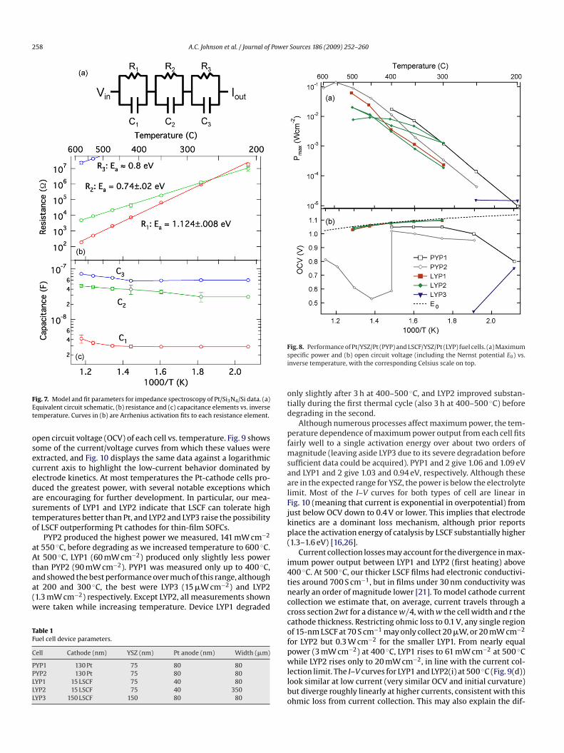
258 A.C. Johnson et al. / Journal of Power Sources 186 (2009) 252–260
FEt
osecedasto
aAtaa(w
TF
C
PPLLL
Fsi
otd
pfmsaalFjkp(
i
ig. 7. Model and fit parameters for impedance spectroscopy of Pt/Si3N4/Si data. (a)quivalent circuit schematic, (b) resistance and (c) capacitance elements vs. inverseemperature. Curves in (b) are Arrhenius activation fits to each resistance element.
pen circuit voltage (OCV) of each cell vs. temperature. Fig. 9 showsome of the current/voltage curves from which these values werextracted, and Fig. 10 displays the same data against a logarithmicurrent axis to highlight the low-current behavior dominated bylectrode kinetics. At most temperatures the Pt-cathode cells pro-uced the greatest power, with several notable exceptions whichre encouraging for further development. In particular, our mea-urements of LYP1 and LYP2 indicate that LSCF can tolerate highemperatures better than Pt, and LYP2 and LYP3 raise the possibilityf LSCF outperforming Pt cathodes for thin-film SOFCs.
PYP2 produced the highest power we measured, 141 mW cm−2
t 550 ◦C, before degrading as we increased temperature to 600 ◦C.t 500 ◦C, LYP1 (60 mW cm−2) produced only slightly less power
han PYP2 (90 mW cm−2). PYP1 was measured only up to 400 ◦C,
nd showed the best performance over much of this range, althought 200 and 300 ◦C, the best were LYP3 (15 �W cm−2) and LYP21.3 mW cm−2) respectively. Except LYP2, all measurements shownere taken while increasing temperature. Device LYP1 degradedable 1uel cell device parameters.
ell Cathode (nm) YSZ (nm) Pt anode (nm) Width (�m)
YP1 130 Pt 75 80 80YP2 130 Pt 75 80 80YP1 15 LSCF 75 40 80YP2 15 LSCF 75 40 350YP3 150 LSCF 150 80 80
4tncccofpwllbo
ig. 8. Performance of Pt/YSZ/Pt (PYP) and LSCF/YSZ/Pt (LYP) fuel cells. (a) Maximumpecific power and (b) open circuit voltage (including the Nernst potential E0) vs.nverse temperature, with the corresponding Celsius scale on top.
nly slightly after 3 h at 400–500 ◦C, and LYP2 improved substan-ially during the first thermal cycle (also 3 h at 400–500 ◦C) beforeegrading in the second.
Although numerous processes affect maximum power, the tem-erature dependence of maximum power output from each cell fits
airly well to a single activation energy over about two orders ofagnitude (leaving aside LYP3 due to its severe degradation before
ufficient data could be acquired). PYP1 and 2 give 1.06 and 1.09 eVnd LYP1 and 2 give 1.03 and 0.94 eV, respectively. Although thesere in the expected range for YSZ, the power is below the electrolyteimit. Most of the I–V curves for both types of cell are linear inig. 10 (meaning that current is exponential in overpotential) fromust below OCV down to 0.4 V or lower. This implies that electrodeinetics are a dominant loss mechanism, although prior reportslace the activation energy of catalysis by LSCF substantially higher1.3–1.6 eV) [16,26].
Current collection losses may account for the divergence in max-mum power output between LYP1 and LYP2 (first heating) above00 ◦C. At 500 ◦C, our thicker LSCF films had electronic conductivi-ies around 700 S cm−1, but in films under 30 nm conductivity wasearly an order of magnitude lower [21]. To model cathode currentollection we estimate that, on average, current travels through aross section 2wt for a distance w/4, with w the cell width and t theathode thickness. Restricting ohmic loss to 0.1 V, any single regionf 15-nm LSCF at 70 S cm−1 may only collect 20 �W, or 20 mW cm−2
or LYP2 but 0.3 W cm−2 for the smaller LYP1. From nearly equalower (3 mW cm−2) at 400 ◦C, LYP1 rises to 61 mW cm−2 at 500 ◦Chile LYP2 rises only to 20 mW cm−2, in line with the current col-
ection limit. The I–V curves for LYP1 and LYP2(i) at 500 ◦C (Fig. 9(d))ook similar at low current (very similar OCV and initial curvature)ut diverge roughly linearly at higher currents, consistent with thishmic loss from current collection. This may also explain the dif-

A.C. Johnson et al. / Journal of Power Sources 186 (2009) 252–260 259
Fc
ig. 9. Current/voltage sweeps for various cells at (a) 200 ◦C, (b) 300 ◦C, (c) 400 ◦C, and (dooling, and (iii) second heating. At 400 ◦C (c), two traces of PYP2 are shown, before and a
Fig. 10. The same data as Fig. 9 again
) 500 ◦C. For LYP2, Roman numerals denote sweeps during (i) the first heating, (ii)fter an OCV drop.
st a logarithmic current axis.

2 Power
f2
o2acamwlnspcgdcPr
tomvAmhfPdtbadt3wALp
4
Lbft5i
ioipaal
A
tfisR
R
[[[
[[
[[
[[
[[
[
[
60 A.C. Johnson et al. / Journal of
erence in maximum power activation energy between LYP1 and.
Between 350 and 450 ◦C, LYP1 and 2 have OCVs within 10 mVf the thermodynamic limit (dashed curve in Fig. 8b), and within5 mV at 300 and 500 ◦C. PYP1 and 2, however, are at least 30 mVnd often over 100 mV below the limit. Moreover, some Pt-cathodeells abruptly and irreversibly drop to much lower OCV, as PYP2 didt 400 ◦C—the two PYP2 curves in Fig. 9(c), for example, were takeninutes apart. Both before and after such a drop, OCV increasesith temperature, indicating electronic or gaseous leakage that is
ess temperature dependent than ionic resistance. These drops areot correlated with mechanical breakdown, implying that Pt diffu-ion, possibly via grain boundaries or pinholes in the YSZ, may formartial electrical shorts. In contrast, OCV drops in LSCF-cathodeells tend to presage visible cracks, implying that small cracks andas leakage cause these drops. LYP3 outperformed PYP1 at 200 ◦Cespite an already lower OCV, implying that if these mechanicalonstraints can be addressed LSCF can be expected to outperformt as a cathode material throughout the intermediate temperatureange.
A close examination of Fig. 9(c) provides some insight intohe performance differences between cells with LSCF and Pt cath-des. An unusual effect is observed which, if it can be understood,ay lead to substantially improved power output. Each current-
oltage sweep was taken by fixing voltage and measuring current.t low current they all look similar (except for the second measure-ent of PYP2, after its OCV dropped). LYP1 and LYP2 have slightly
igher OCV and exchange current (20–50 �A cm−2 vs. 10 �A cm−2
or PYP1) but lower transfer coefficient (0.53–0.63 vs. 0.72 forYP1). However, at higher current a reversible time- and voltage-ependent loss affects LYP1 and LYP2. At voltages well below OCV,he current drops with time, in some cases curving the I–V sweepackward. Jumps in the data, visible for example on the LYP1 curvet around 0.25 and 0.1 V, are not noise but rather places currentropped more when the sweep paused during an update of theemperature controller. In one instance, the cell was left at V = 0 for0 min and current decreased an order of magnitude. After this OCVas only 0.8 V, but recovered its initial value after 30 min at I = 0.fter cycling to other temperatures, subsequent measurements ofYP2 at the same temperature this effect diminished, increasingower output substantially.
. Conclusions
This study has demonstrated functional thin-film SOFCs withSCF cathodes made by sputtering, etching, and lithography. To the
est of our knowledge, this is the first report describing functionaluel cells with RF-sputtered LSCF ultra-thin films from a compositearget. Maximum power output of ∼60 mW cm−2 was obtained at00 ◦C with LSCF cathodes, which is comparable to results reportedn the literature using similar micro-fabrication approaches utiliz-
[[[
[
Sources 186 (2009) 252–260
ng ultra-thin-film oxides. Deposition techniques enabling rougherr porous LSCF surfaces could further improve performance byncreasing the area for catalysis. Impedance characteristics of fullyrocessed devices as well as various component layers have beennalyzed as a function of temperature and presented. The resultsre encouraging towards the use of non-precious metal cathodes forow and intermediate temperature thin-film solid oxide fuel cells.
cknowledgments
We thank Antonio Baclig, Amrita Saigal, and the Rowland Insti-ute at Harvard staff for technical support. The authors acknowledgenancial support from SiEnergy Systems, the Harvard Univer-ity Center for the Environment, and the Eppley Foundation foresearch.
eferences
[1] B.C.H. Steele, A. Heinzel, Nature 414 (2001) 345–352.[2] S.M. Haile, Acta Mater. 51 (2003) 5981–6000.[3] V.V. Kharton, F.M.B. Marques, A. Atkinson, Solid State Ionics 174 (2004)
135–149.[4] C.D. Baertsch, K.F. Jensen, J.L. Hertz, H.L. Tuller, S.T. Vengallatore, S.M. Spearing,
M.A. Schmidt, J. Mater. Res. 19 (2004) 2604–2615.[5] H. Huang, M. Nakamura, P. Su, R. Fasching, Y. Saito, F.B. Prinz, J. Electrochem.
Soc. 154 (2007) B20–24.[6] A. Bieberle-Hutter, D. Beckel, A. Infortuna, U.P. Muecke, J.L.M. Rupp, L.J. Gauckler,
S. Rey-Mermet, P. Muralt, N.R. Bieri, N. Hotz, M.J. Stutz, D. Poulikakos, P. Heeb,P. Muller, A. Bernand, R. Gmur, T. Hocker, J. Power Sources 177 (2008) 123–130.
[7] I. Kosacki, C.M. Rouleau, P.F. Becher, J. Bentley, D.H. Lowndes, Electrochem.Solid-State Lett. 7 (2004) A459–A461.
[8] S. Azad, O.A. Marina, C.M. Wang, L. Saraf, V. Shutthanandan, D.E. McCready, A.El-Azab, J.E. Jaffe, M.H. Engelhard, C.H.F. Peden, S. Thevuthasan, Appl. Phys. Lett.86 (2005) 131906.
[9] X. Guo, E. Vasco, S. Mi, K. Szot, E. Wachsman, R. Waser, Acta Mater. 53 (2005)5161–5166.
10] H. Huang, T.M. Gur, Y. Saito, F.B. Prinz, Appl. Phys. Lett. 89 (2006) 143107.11] A. Karthikeyan, C.-L. Chang, S. Ramanathan, Appl. Phys. Lett. 89 (2006) 183116.12] J. Garcia-Barriocanal, A. Rivera-Calzada, M. Varela, Z. Sefrioui, E. Iborra, C. Leon,
S.J. Pennycook, J. Santamaria, Science 321 (2008) 676–680.13] J.H. Shim, C.-C. Chao, H. Huang, F.B. Prinz, Chem. Mater. 19 (2007) 3850–3854.14] L.-W. Tai, M.M. Nasrallah, H.U. Anderson, D.M. Sparlin, S.R. Sehlin, Solid State
Ionics 76 (1995) 259–271.15] Z. Shao, S.M. Haile, Nature 431 (2004) 170–173.16] F.S. Baumann, J. Fleig, G. Cristiani, B. Stuhlhofer, H.-U. Habermeier, J. Maier, J.
Electrochem. Soc. 154 (2007) B931–B941.17] A.E. Kaloyeros, E. Eisenbraun, Annu. Rev. Mater. Sci. 30 (2000) 363–385.18] G. Bilger, T. Voss, T. Schlenker, A. Strohm, Surf. Interface Anal. 38 (2006)
1687–1691.19] H. Schmidt, U. Geckle, M. Bruns, Phys. Rev. B 74 (2006) 045203.20] J.L. Hertz, A. Rothschild, H.L. Tuller, J. Electroceram. (2008), doi:10.1007/s10832-
008-9475-5.21] B.-K. Lai, A.C. Johnson, H. Xiong, S. Ramanathan, J. Power Sources 186 (2009)
115–122.22] S.P. Simner, M.D. Anderson, M.H. Engelhard, J.W. Stevenson, Electrochem. Solid-
State Lett. 9 (2006) A478–A481.23] J.H. Joo, G.M. Choi, Solid State Ionics 177 (2006) 1053–1057.24] X. Guo, R. Waser, Prog. Mater. Sci. 51 (2006) 151–210.25] N.Q. Minh, T. Takahashi, Science and Technology of Ceramic Fuel Cells, Elsevier,
Amsterdam, 1995, p. 94.26] S.P. Jiang, Solid State Ionics 146 (2002) 1–22.


