Influence of bias voltage on the crystallographic orientation and morphology of sputter deposited...
7
pss current topics in solid state physics c status solidi www.pss-c.com physica REPRINT Influence of bias voltage on the crystallographic orientation and morphology of sputter deposited yttria stabilized zirconia (YSZ) thin films C. Amaya 1 , J. Caicedo 1,2 , G. Bejarano 2, 4 , C. A. Cortés Escobedo 3 , J. Muñoz-Saldaña 3 , G. Zambrano 1 , and P. Prieto 1 1 Thin Films Group, Excellence Center for Novel Materials, Universidad del Valle, Cali, Colombia 2 Hard Coatings Laboratory, CDT-ASTIN SENA, Cali, Colombia 3 Center for Investigation and Advanced Studies, CINVESTAV-IPN, Querétaro, México 4 Group of Corrosion and Protection, Antioquia University, Medellín, Colombia Received 16 October 2006, revised 13 March 2007, accepted 30 May 2007 Published online 26 October 2007 PACS 68.35.Bs, 68.55.Jk, 68.55.Nq, 81.15.Cd ZrO 2 -8% mol. Y 2 O 3 (8YSZ) thin films were deposited onto silicon [100] and AISI 304 stainless steel sub- strates by r.f. (13.56 MHz) multi-target magnetron sputtering. To improve the adhesion of a YSZ mono- layer to the stainless steel substrate, a buffer layer of Al 2 O 3 was incorporated too. Crystal structure and Infrared (IR) absorption bands of YSZ were investigated as functions of substrate bias by X-ray diffracti- on (XRD) and Fourier Transformed Infrared Spectroscopy (FTIR), respectively. The influence of the bias voltage on the roughness, grain size, and microstructure of deposited thin films was determined by AFM and SEM. XRD results show the presence of a tetragonal phase with [111] and [200] orientations. On the other hand, FTIR spectra exhibit the 2E u and F 1u modes as two broad bands in the frequency range of 450 ~ 550 cm –1 and 550 ~ 650 cm –1 , corresponding to the tetragonal and cubic phases of ZrO 2 , respectively. In this work we present the systematic influence of the bias voltage on the crystalline structure, the presence of the tetragonal phase and morphology of the YSZ thin films. The XRD, FTIR, and AFM results indicate that when the bias voltage increases from -20 V to -60 V the preferential crystallographic orientation of YSZ tetragonal phase changes from [111] to [200], and the percentage of the tetragonal phase diminishes, as well as the grain size of deposited films from (560 ± 5) to (470 ± 5) nm. phys. stat. sol. (c) 4, No. 11, 4288– 4293 (2007) / DOI 10.1002/pssc.200675925
-
Upload
independent -
Category
Documents
-
view
2 -
download
0
Transcript of Influence of bias voltage on the crystallographic orientation and morphology of sputter deposited...

p s scurrent topics in solid state physics
c
statu
s
soli
di
www.pss-c.comph
ysi
ca
REPRINT
Influence of bias voltage on the crystallographic orientation
and morphology of sputter deposited yttria stabilized zirconia
(YSZ) thin films
C. Amaya1
, J. Caicedo1,2
, G. Bejarano2, 4
, C. A. Cortés Escobedo3
, J. Muñoz-Saldaña3
,
G. Zambrano1
, and P. Prieto1
1
Thin Films Group, Excellence Center for Novel Materials, Universidad del Valle, Cali, Colombia
2
Hard Coatings Laboratory, CDT-ASTIN SENA, Cali, Colombia
3
Center for Investigation and Advanced Studies, CINVESTAV-IPN, Querétaro, México
4
Group of Corrosion and Protection, Antioquia University, Medellín, Colombia
Received 16 October 2006, revised 13 March 2007, accepted 30 May 2007
Published online 26 October 2007
PACS 68.35.Bs, 68.55.Jk, 68.55.Nq, 81.15.Cd
ZrO2-8% mol. Y
2O
3(8YSZ) thin films were deposited onto silicon [100] and AISI 304 stainless steel sub-
strates by r.f. (13.56 MHz) multi-target magnetron sputtering. To improve the adhesion of a YSZ mono-
layer to the stainless steel substrate, a buffer layer of Al2O
3was incorporated too. Crystal structure and
Infrared (IR) absorption bands of YSZ were investigated as functions of substrate bias by X-ray diffracti-
on (XRD) and Fourier Transformed Infrared Spectroscopy (FTIR), respectively. The influence of the bias
voltage on the roughness, grain size, and microstructure of deposited thin films was determined by AFM
and SEM. XRD results show the presence of a tetragonal phase with [111] and [200] orientations. On the
other hand, FTIR spectra exhibit the 2Eu
and F1u
modes as two broad bands in the frequency range of 450
~ 550 cm–1
and 550 ~ 650 cm–1
, corresponding to the tetragonal and cubic phases of ZrO2, respectively. In
this work we present the systematic influence of the bias voltage on the crystalline structure, the presence
of the tetragonal phase and morphology of the YSZ thin films. The XRD, FTIR, and AFM results indicate
that when the bias voltage increases from -20 V to -60 V the preferential crystallographic orientation of
YSZ tetragonal phase changes from [111] to [200], and the percentage of the tetragonal phase diminishes,
as well as the grain size of deposited films from (560 ± 5) to (470 ± 5) nm.
phys. stat. sol. (c) 4, No. 11, 4288–4293 (2007) / DOI 10.1002/pssc.200675925

phys. stat. sol. (c) 4, No. 11, 4288–4293 (2007) / DOI 10.1002/pssc.200675925
© 2007 WILEY-VCH Verlag GmbH & Co. KGaA, Weinheim
Influence of bias voltage on the crystallographic orientation
and morphology of sputter deposited yttria stabilized zirconia
(YSZ) thin films
C. Amaya∗,1
, J. Caicedo1,2
, G. Bejarano2, 4
, C. A. Cortés Escobedo3, J. Muñoz-Saldaña
3,
G. Zambrano1, and P. Prieto
1
1 Thin Films Group, Excellence Center for Novel Materials, Universidad del Valle, Cali, Colombia 2 Hard Coatings Laboratory, CDT-ASTIN SENA, Cali, Colombia 3 Center for Investigation and Advanced Studies, CINVESTAV-IPN, Querétaro, México 4 Group of Corrosion and Protection, Antioquia University, Medellín, Colombia
Received 16 October 2006, revised 13 March 2007, accepted 30 May 2007
Published online 26 October 2007
PACS 68.35.Bs, 68.55.Jk, 68.55.Nq, 81.15.Cd
ZrO2-8% mol. Y2O3 (8YSZ) thin films were deposited onto silicon [100] and AISI 304 stainless steel sub-
strates by r.f. (13.56 MHz) multi-target magnetron sputtering. To improve the adhesion of a YSZ mono-
layer to the stainless steel substrate, a buffer layer of Al2O3
was incorporated too. Crystal structure and
Infrared (IR) absorption bands of YSZ were investigated as functions of substrate bias by X-ray diffracti-
on (XRD) and Fourier Transformed Infrared Spectroscopy (FTIR), respectively. The influence of the bias
voltage on the roughness, grain size, and microstructure of deposited thin films was determined by AFM
and SEM. XRD results show the presence of a tetragonal phase with [111] and [200] orientations. On the
other hand, FTIR spectra exhibit the 2Eu
and F1u
modes as two broad bands in the frequency range of 450
~ 550 cm–1
and 550 ~ 650 cm–1, corresponding to the tetragonal and cubic phases of ZrO2, respectively. In
this work we present the systematic influence of the bias voltage on the crystalline structure, the presence
of the tetragonal phase and morphology of the YSZ thin films. The XRD, FTIR, and AFM results indicate
that when the bias voltage increases from -20 V to -60 V the preferential crystallographic orientation of
YSZ tetragonal phase changes from [111] to [200], and the percentage of the tetragonal phase diminishes,
as well as the grain size of deposited films from (560 ± 5) to (470 ± 5) nm.
© 2007 WILEY-VCH Verlag GmbH & Co. KGaA, Weinheim
1 Introduction
Yttria stabilized zirconia materials (YSZ) have been extensively studied given that they exhibit novel
properties such as low thermal conductivity, high thermal coefficient expansion, high hardness (as com-
pared to other ceramics) and corrosion resistance at high temperatures. These films have been used as
optical devices [1], buffer layers of YBa2Cu3O7-x superconductive thin films [2] and protective coatings
[3]. For the pure zirconia stable form at room temperature is monoclinic, but there is a transition at about
1170 ºC to a tetragonal form. This transition is accompanied by a large volume change (3-5%), and a
disruption of ceramic bodies made with a pure zirconia results. However, this can be inhibited by the
addition of a convenient amount of other oxides, such as CaO, MgO, and Y2O3 [4], which retained the
tetragonal phase at room temperature. The mechanical and thermal properties of zirconia-based materials
are known to be a function of phase structure and microstructure [5].
∗ Corresponding author: e-mail: [email protected], Phone: +57 2 339-4610-Ext 42

phys. stat. sol. (c) 4, No. 11 (2007) 4289
www.pss-c.com © 2007 WILEY-VCH Verlag GmbH & Co. KGaA, Weinheim
Tetragonal zirconia exhibits high strength and toughness because tetragonal-monoclinic transformation
whose main requirement is that a high temperature tetragonal phase can be retained at room temperature.
Also, several studies have demonstrated the dependence of thermal conductivity to grain size, when this
decreases to the nanometer range [6, 7], due to phonon scattering by an increment in the volume fraction
of grain boundaries or interfaces. The rapid progress in the synthesis and processing of materials with the
structure on nanometer scale has increased interest in the manufacture tetragonal zirconia thin films that
operate as insulating thermal with phase stability at high temperatures. A variety of techniques have been
used to deposit YSZ, including plasma spray [8], electron beam physical vapor deposition [9], and sol
gel process [10].
Among these techniques, the magnetron sputtering methods are suitable technologies to deposit ceramic
coatings whose crystal structure and microstructure are strongly dependent on processing parameters
such as pressure sputtering, distance substrate-target and sputtering power [11, 12]. ZrO2 thin films sho-
wed orientation preference and change in morphology when formed under ion bombardment [13]. In this
article, we analyzed the effect of applied substrate bias voltage when increased from -20 V to -60 V on
the crystalline structure, the presence of the tetragonal phase, and morphology of ZrO2-8% mol. Y2O3
thin films.
2 Experimental details
ZrO2-8% mol.Y2O3 films (8YSZ) and Al2O3/8YSZ layers were prepared via r.f (13.56 MHz) magnetron
sputtering method in an Ar atmosphere (purity 99.99%) at a power of 350 W. For film deposition we
used a target of zirconia of 4 inches in diameter doped with 8% mol. yttria and a target of Al (purity
99.99%). The films were deposited onto silicon (100 orientation) and AISI 304 stainless substrates. The
substrates were ultrasonically cleaned in a sequence of acetone and ethanol during 20 minutes for each
cycle. Before the deposition process, the vacuum chamber was evacuated, using a turbomolecular pump
at a pressure of 7.2 x 10⁻⁵ mbar to reduce the effects of the residual air. Within of the chamber, the sub-
strates were subjected for 15 minutes to a bias voltage of -400V at power of 60W (r.f) in an argon plasma
to remove any oxide layer. A gradient bond coat with a compositionally graded structure of Al+Al2O3
was deposited onto steel substrates, using oxygen (purity 99.99%) as a working gas, which flow it was
increased by means standard mass-flow controllers (MKS 247-D) each 3.5 minutes until total time of 20
minutes. Both the bond coat and 8YSZ thin films were deposited at work pressure of 7.0 x 10⁻³ mbar.
During the deposition process the temperature was maintained at 300ºC and the distance between sub-
strate and target was 60 mm to guarantee a homogeneous thickness of layers.
The applied substrate bias was increased from -20 V to -60 V to evaluate its effect on the crystal structu-
re, morphology and microstructure of the deposited films. The crystal structure of 8YSZ films grown
onto AISI 304 steel was characterized by X-ray diffraction (XRD) by using Cu Kα radiation. The 2θ
scanning range was from 20 to 70º. For the infrared analysis (IR) the samples were grown on silicon
substrates and the spectra were recorded in the transmission mode with an 8400 Shimatzu FTIR
spectrometer which uses a Nerst-type ceramic source. Surface roughness, grain size, and morphological
studies were determined by means of AFM (Autoprobe CP Park Scientific Instrument) in contact mode.
The cross section microstructure of the films was investigated by a high resolution Scanning Electron
Microscope operating at 30kV.
3 Results and discussion
Figure 1 shows XRD patterns of deposited ZrO2-8% mol. Y2O3 thin films as a function of the applied
substrate bias potential. These patterns displayed multiple strong diffraction peaks, which were identified
as the [111], [200], [220] and [311] tetragonal reflections. In addition to the strong tetragonal peaks, was
observed at 2θ = 43.6º a peak corresponding to AISI 304 stainless steel. From Fig. 1, we can observe that
when the substrate bias was varied from -20 V to -60 V, [111]t and [200]t tetragonal peaks dominated,

4290 C. Amaya et al.: Crystallographic orientation and morphology of sputter deposited YSZ thin films
© 2007 WILEY-VCH Verlag GmbH & Co. KGaA, Weinheim www.pss-c.com
indicating that the films were primarily composed of metastable tetragonal zirconia, and the preferential
crystallographic orientation of the YSZ tetragonal phase changes from [111] to [200]; we also observe a
shift of these peaks. This suggests that there is some effect from the biasing voltage on the films.
20 25 30 35 40 45 50 55 60 65 70
Inte
nsity
(a.
u.)
- 60V
[311]t[1 1 1]t [220]t
- 40V
- 20V
2θ
Steel
[200]t
Fig. 1 XRD patterns of Al2O3/8YSZ thin films grown onto AISI 304 steel at different substrate bias.
The degree of crystallographic orientation is heavily dependent on the processing parameters. Its should
be noted that shifts in the intensity of the peaks results from de lattice distortion and are generally associ-
ated to compressive residual strains originated from an ion bombardment. Films deposited at no bias
voltage would have a [111] orientation as it has the lowest surface energy. However, under substrate bias
voltage applied results in residual strains that compete with the surface energy, which determines the
orientation of the film during growth. The application of a bias voltage increases the surface mobility
leading to the formation of a coating with more structural perfection [14], promoting closed packed
structures in near-thermodynamic equilibrium conditions [15]. Thus, for high atomic mobility, the YSZ
films are expected to grow along the [200] orientation corresponding to that with the lowest surface free
energy [16]. For low atomic mobility (low bias) the preferred orientation is the [111] in which the hig-
hest number of atoms per unit area can be incorporated at low energy sites. The preference for the [200]
orientation observed in the current study is opposite to other works [13, 17], which have demonstrated
that ZrO2 and YSZ thin films deposited under greater bias voltage, presented a shift in the preferred
orientation from [200] to [111] when substrate bias was increased to values near to -400 V, because the
increase of the ion bombardment created sufficient damage to the lattice structure to return it to the [111]
orientation. This effect is observed in TiN films also deposited under bias voltage [18].
FTIR spectroscopy can be used as a complementary technique with XRD for further bonding characteri-
zation of the YSZ thin films. Figure 2 shows FTIR spectra for the samples grown onto silicon substrates
without bond coat. Typical frequencies of the vibrational modes of the YSZ are reported in Table 1.
Table 1 IR vibrational modes for monoclinic, tetragonal, and cubic YSZ.
Phase Symmetry λ (cm–1
) Ref.
Monoclinic 8Au+7Bu 740 [19]
Tetragonal A2u + 2Eu
164, 467
339
[20]
Cubic F1u 358, 628 [20, 21]

phys. stat. sol. (c) 4, No. 11 (2007) 4291
www.pss-c.com © 2007 WILEY-VCH Verlag GmbH & Co. KGaA, Weinheim
800 750 700 650 600 550 500 450 400
TRANSMITTANCE
-20V
Wavenumber (cm-1)
-40V
-8YSZ 740
621
462
-60V
Fig. 2 Infrared transmission spectra of 8YSZ thin films. Curves correspond to samples deposited at different substra-
te bias.
By comparing of our spectra to reported values, it is clear that the samples mainly consist of the tetrago-
nal phase, so the infrared transmission curves are similar, exhibiting the 2Eu mode as one broad band at
462 cm–1. With less intensity in the spectrum, we observed two small shoulders at 740 cm–1 and 621 cm–1
associated to monoclinic and cubic phases, respectively. Infrared spectroscopy analysis confirmed that
for the 8YSZ samples deposited under our conditions, there was no occurrence of any tetragonal-
monoclinic transition at values of applied bias voltage.
AFM images of the films are shown in Fig. 3. A first assessment of the images reveals that the films are
formed by spheroid and elongated grains. From the AFM analysis, as seen in Table 2, we can establish
that the increase of the bias voltage causes a decrease in the grain size and an increase of the surface
roughness.
Fig. 3 AFM images of 8YSZ thin films deposited at (a) -20 V, (b) -40 V and (c) -60 V. 5 x 5 µm.
4292 C. Amaya et al.: Crystallographic orientation and morphology of sputter deposited YSZ thin films
© 2007 WILEY-VCH Verlag GmbH & Co. KGaA, Weinheim www.pss-c.com
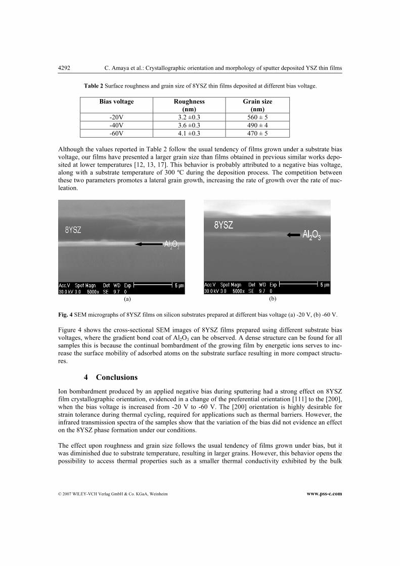
Table 2 Surface roughness and grain size of 8YSZ thin films deposited at different bias voltage.
Bias voltage
Roughness
(nm)
Grain size
(nm)
-20V 3.2 ±0.3 560 ± 5
-40V 3.6 ±0.3 490 ± 4
-60V 4.1 ±0.3 470 ± 5
Although the values reported in Table 2 follow the usual tendency of films grown under a substrate bias
voltage, our films have presented a larger grain size than films obtained in previous similar works depo-
sited at lower temperatures [12, 13, 17]. This behavior is probably attributed to a negative bias voltage,
along with a substrate temperature of 300 ºC during the deposition process. The competition between
these two parameters promotes a lateral grain growth, increasing the rate of growth over the rate of nuc-
leation.
(a)
(b)
Fig. 4 SEM micrographs of 8YSZ films on silicon substrates prepared at different bias voltage (a) -20 V, (b) -60 V.
Figure 4 shows the cross-sectional SEM images of 8YSZ films prepared using different substrate bias
voltages, where the gradient bond coat of Al2O3 can be observed. A dense structure can be found for all
samples this is because the continual bombardment of the growing film by energetic ions serves to inc-
rease the surface mobility of adsorbed atoms on the substrate surface resulting in more compact structu-
res.
4 Conclusions
Ion bombardment produced by an applied negative bias during sputtering had a strong effect on 8YSZ
film crystallographic orientation, evidenced in a change of the preferential orientation [111] to the [200],
when the bias voltage is increased from -20 V to -60 V. The [200] orientation is highly desirable for
strain tolerance during thermal cycling, required for applications such as thermal barriers. However, the
infrared transmission spectra of the samples show that the variation of the bias did not evidence an effect
on the 8YSZ phase formation under our conditions.
The effect upon roughness and grain size follows the usual tendency of films grown under bias, but it
was diminished due to substrate temperature, resulting in larger grains. However, this behavior opens the
possibility to access thermal properties such as a smaller thermal conductivity exhibited by the bulk

phys. stat. sol. (c) 4, No. 11 (2007) 4293
www.pss-c.com © 2007 WILEY-VCH Verlag GmbH & Co. KGaA, Weinheim
material. On the other hand, more compact and dense structures can be obtained, allowing enhancement
in mechanical and resistant corrosion properties.
Finally, the inclusion of a gradient of Al2O3 as a bond coat between the ceramic layer and the steel sub-
strate enhances the adherence of the film, allowing the deposit onto AISI 304 steel substrates. The
Al2O3/8YSZ deposited bilayer structure, opens the possibility to coat high-performance elements expo-
sed to elevated operation temperatures.
Acknowledgements This work was supported by the Excellence Center for Novel Materials (ECNM) Colombia,
CDT-ASTIN, SENA Regional Valle, Cali, Colombia, and the Center for Investigation and Advanced Studies (CIN-
VESTAV) Queretaro-México.
References
[1] C. K. Kwok and C. R. Aita, J. Appl. Phys. 66, 2756 (1994).
[2] R. Aguiar, F. Sanchez, C. Ferrater, and M. Varela, Thin Solid Films 306, 74 (1997).
[3] R. D. Maggio, L. Fedrizzi, S. Rossi, and P. Scardi, Thin Solid Films 286, 127 (1996).
[4] H. G. Scott, J. Mater. Sci. 10, 1527 (1975).
[5] T. Masaki, J. Am. Ceram. Soc. 69, 519 (1986).
[6] J. A. Eastman, G. Soyez, G. R. Bai, and L. J. Thompson, Nanostructured Materials for Microstructural Control
of Thermal Properties, invited paper submitted to the Proc. of the NATO Advanced Study Institute on Func-
tional Gradient Materials and Surface Layers prepared by Fine Particle Technology, Kiev, Ukraine, June 18-28
(2000).
[7] Ho-Soon Yang, G.-R. Bai, L. J. Thompson, and J. A. Eastman, Acta Mater. 50, 2309 (2002).
[8] P. Scardi and L. Lutterotti, Surf. Coat. Technol. 61, 52 (1993).
[9] D. D. Hass, A. J. Slifka, and H. N. G. Wadley, Acta Mater. 49, 973 (2001).
[10] A. Meher, H. Klumper-Westkamp, F. Hoffmann, and P. Mayr, Thin Solid Films 308, 673 (1997).
[11] Pengtao Gao, L. J. Meng, M. P. dos Santos, V. Teixeira, and M. Andritschky, Thin Solid Films 377, 557
(2000).
[12] Pengtao Gao, L. J. Meng, M. P. dos Santos, V. Teixeira, and M. Andritschky, Appl. Surf. Sci. 173, 84 (2001).
[13] Zhiqiang Ji and J. M. Risgbee, J. Am. Ceram. Soc. 84, 2841 (2001).
[14] P. Patsalas, C. Charitidis, and S. Logothetidis, Surf. Coat. Technol. 125, 335 (2000).
[15] J. E. Greene, J. E. Sundgren, L. Hultman, I. Petrov, and D. B. Bergstrom, Appl. Phys. Lett. 67, 2928 (1995).
[16] J. E. Greene, in: D. T. J. Hurle (Ed.), Handbook of Crystal Growth, Vol. 1 (Elsevier, Amsterdam, 1993).
[17] Zhiqiang Ji, J. Allen Haynes, E. Voelkl, and J. M. Risgbee, J. Am. Ceram. Soc. 84, 929 (2001).
[18] L. Hultman, W. D. Münz, J. Musil, S. Kadlec, I. Petrov, and J. E. Greene, J. Vac. Sci. Technol. A 9, 434
(1991).
[19] Z. Qian and J. L. Shi, NanoStruct. Mater. 10, 235 (1998).
[20] C. Pecharromán, M. Ocaña, and C. J. Serna, J. Appl. Phys. 80, 33479 (1996).
[21] T. Hirata, E. Asari, and M. Kitajima, J. Solid State Chem. 110, 201 (1994).