Low wavenumber Raman scattering of nanoparticles and nanocomposite materials
Upload
independentCategory
view
1download
0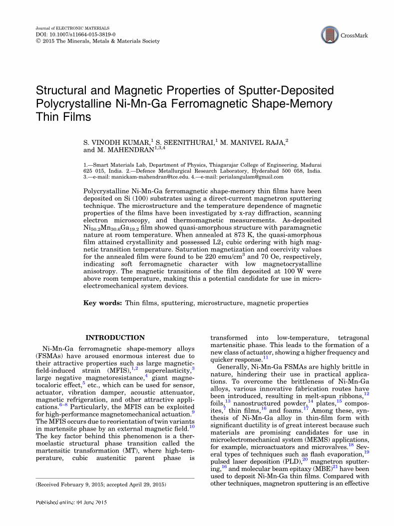
Structural and Magnetic Properties of Sputter-DepositedPolycrystalline Ni-Mn-Ga Ferromagnetic Shape-MemoryThin Films
S. VINODH KUMAR,1 S. SEENITHURAI,1 M. MANIVEL RAJA,2
and M. MAHENDRAN1,3,4
1.—Smart Materials Lab, Department of Physics, Thiagarajar College of Engineering, Madurai625 015, India. 2.—Defence Metallurgical Research Laboratory, Hyderabad 500 058, India.3.—e-mail: [email protected]. 4.—e-mail: [email protected]
Polycrystalline Ni-Mn-Ga ferromagnetic shape-memory thin films have beendeposited on Si (100) substrates using a direct-current magnetron sputteringtechnique. The microstructure and the temperature dependence of magneticproperties of the films have been investigated by x-ray diffraction, scanningelectron microscopy, and thermomagnetic measurements. As-depositedNi50.2Mn30.6Ga19.2 film showed quasi-amorphous structure with paramagneticnature at room temperature. When annealed at 873 K, the quasi-amorphousfilm attained crystallinity and possessed L21 cubic ordering with high mag-netic transition temperature. Saturation magnetization and coercivity valuesfor the annealed film were found to be 220 emu/cm3 and 70 Oe, respectively,indicating soft ferromagnetic character with low magnetocrystallineanisotropy. The magnetic transitions of the film deposited at 100 W wereabove room temperature, making this a potential candidate for use in micro-electromechanical system devices.
Key words: Thin films, sputtering, microstructure, magnetic properties
INTRODUCTION
Ni-Mn-Ga ferromagnetic shape-memory alloys(FSMAs) have aroused enormous interest due totheir attractive properties such as large magnetic-field-induced strain (MFIS),1,2 superelasticity,3
large negative magnetoresistance,4 giant magne-tocaloric effect,5 etc., which can be used for sensor,actuator, vibration damper, acoustic attenuator,magnetic refrigeration, and other attractive appli-cations.6–8 Particularly, the MFIS can be exploitedfor high-performance magnetomechanical actuation.9
The MFIS occurs due to reorientation of twin variantsin martensite phase by an external magnetic field.10
The key factor behind this phenomenon is a ther-moelastic structural phase transition called themartensitic transformation (MT), where high-tem-perature, cubic austenitic parent phase is
transformed into low-temperature, tetragonalmartensitic phase. This leads to the formation of anew class of actuator, showing a higher frequency andquicker response.11
Generally, Ni-Mn-Ga FSMAs are highly brittle innature, hindering their use in practical applica-tions. To overcome the brittleness of Ni-Mn-Gaalloys, various innovative fabrication routes havebeen introduced, resulting in melt-spun ribbons,12
foils,13 nanostructured powder,14 plates,15 compos-ites,7 thin films,16 and foams.17 Among these, syn-thesis of Ni-Mn-Ga alloy in thin-film form withsignificant ductility is of great interest because suchmaterials are promising candidates for use inmicroelectromechanical system (MEMS) applications,for example, microactuators and microvalves.18 Sev-eral types of techniques such as flash evaporation,19
pulsed laser deposition (PLD),20 magnetron sputter-ing,16 and molecular beam epitaxy (MBE)21 have beenused to deposit Ni-Mn-Ga thin films. Compared withother techniques, magnetron sputtering is an effective(Received February 9, 2015; accepted April 29, 2015)
Journal of ELECTRONIC MATERIALS
DOI: 10.1007/s11664-015-3819-0� 2015 The Minerals, Metals & Materials Society
technique to tailor the composition of the film,which influences the saturation magnetization,martensitic transformation temperature, Curietemperature, and magnetocrystalline anisotropy.22
In addition, magnetron sputtering has the advan-tages of low level of impurities in the film, easycontrol of deposition rate, and low surface rough-ness. Subsequently, production of thin films withvarious morphologies and crystallographic struc-tures has also been shown to be an added advan-tage of this technique.23 Furthermore, thesputtering process is more suitable for integrationof these films with MEMS fabrication technology.Hence, sputtering is an effective technique to pro-duce Ni-Mn-Ga thin films,17,24 being widely used incommercial coating technology.
A lot of studies have been carried out on Ni-Mn-Ga epitaxial films, because of their good shape-memory properties.25–30 Moreover, fabrication ofpolycrystalline shape-memory films with a sub-strate is of great interest among researchers. Pre-viously, a few studies have reported on Ni-Mn-Gathin films grown on various substrates such asAl2O3,31 NaCl,32 MgO,33 and Si.34 Among these,single-crystal silicon is a widely used substrate forMEMS and microsystems, because it can be easilyintegrated with electronics on the same substratefor signal transduction. Moreover, transferablemicrofabrication processes are well established anddocumented for silicon substrates for makingactuators. Hence, tremendous interest has devel-oped in recent years in fabrication of Ni-Mn-Ga thinfilms on silicon substrates. However, thin filmsdeposited on silicon substrates often containresidual stress, affecting the crystallinity, formationof martensitic twins, and magnetic properties.35–37
In addition, the substrate type, sputtering power,argon pressure, and temperature during depositionplay a vital role in determining the film properties.Subsequent postannealing also influences the phasestructure, magnetic ordering, and grain growth,which determine the ferromagnetic and shape-memory properties. Previously, many studies havereported that film deposited at room temperature ispartially crystalline or disordered in nature withoutexhibiting ferromagnetic behavior or shape-memoryproperties.34,38,39 Postdeposition annealing at high-er temperature has been shown to increase thestructural ordering and enhance the shape-memoryeffect outstandingly.34 However, it has also beenshown that high-temperature annealing causesNi-rich phase, which acts as pinning centers fordomain wall motion. This hinders reorientation ofmartensitic twin variants.39 As a result, such film isnot suitable for shape-memory applications. In ad-dition, for annealing temperatures higher than673 K, diffusion of silicon into the film wasobserved, which leads to formation of silicides suchas Mn12Ni4Si3 and Mn15Si26.40 After crystallization,the silicon atoms diffuse easily and the precipitates(silicides) start to grow faster at higher temperature
because the activation energy for crystallization isvery low.41 Silicide formation degrades the filmquality, and the ferromagnetic ordering transformsinto paramagnetic behavior. This confirms thatsilicon diffusion affects the exchange interactionbetween ferromagnetic Ni and Mn atoms via dia-magnetic Si atoms in the crystal sublattice. It is wellknown that the indirect exchange interaction be-tween Mn–Mn atoms plays a key role in the ferro-magnetic ordering in this system. Hakola et al. andBayer et al. also reported that the loss of ferro-magnetism at elevated temperature can mainly beattributed to the formation of Ni-rich phase andsilicon diffusion.42,43 Therefore, to control the for-mation of silicides and Ni-rich precipitates, oneshould select a suitable annealing temperature andholding time, being a crucial issue when Ni-Mn-Ga/Si-based thin films are fabricated for actuatorapplications.
Hence, the present work aims to investigate theeffect of postannealing on the structure and mag-netic properties and studies the residual stresspresent in Ni-Mn-Ga/Si thin films obtained using adirect-current (DC) magnetron sputtering system.In this paper, it is shown that annealing Ni-Mn-Gafilm, even at higher temperature (873 K), enhancesits structural and magnetic properties. We haveaddressed the absence of line precipitates, Ni-richsecondary phase, and silicon diffusion in the afore-mentioned films at high temperature.
EXPERIMENTAL PROCEDURES
High-purity (99.999%) raw elements nickel, man-ganese, and gallium were used to prepare Ni-Mn-Gapolycrystalline alloy using a conventional arc-melt-ing furnace. To attain better chemical homogeneityin the sample, the pancake (ingot) was reverted andremelted for four times. The composition of thesputtering target was found to be Ni50.2Mn30.6Ga19.2
(all compositions in this paper are given in atomicpercent) using inductively coupled plasma opticalemission spectroscopy (ICP-OES, Optima 5300 DV;PerkinElmer). The details of the deposition condi-tions are given in Table I. As-deposited films wereannealed at 873 K for 30 min in a high-temperaturevacuum furnace. Generally, Ni-Mn-Ga thin filmprepared at room temperature is amorphous ordisordered and does not exhibit any appreciablemagnetic ordering. Hence, a thermal annealingprocess is indispensable to obtain magnetism in thissystem.
X-ray diffraction (XRD, PW 1320; Philips) analy-sis was carried out at room temperature using CuKa radiation to examine the film structure, such aspreferred orientation and crystallinity. The surfacemorphology of the films was observed using scan-ning electron microscopy (SEM, LEO 440i) with anultracool energy-dispersive x-ray SiLi detector. Themicrostructure of the film was measured by atomicforce microscopy. Magnetic and thermomagnetic
Vinodh Kumar, Seenithurai, Manivel Raja, and Mahendran
studies of the films were carried out using avibrating-sample magnetometer (VSM-883A) andQuantum Design SQUID-VSM in the temperaturerange from 4 K to 400 K.
RESULTS AND DISCUSSION
Structural Analysis
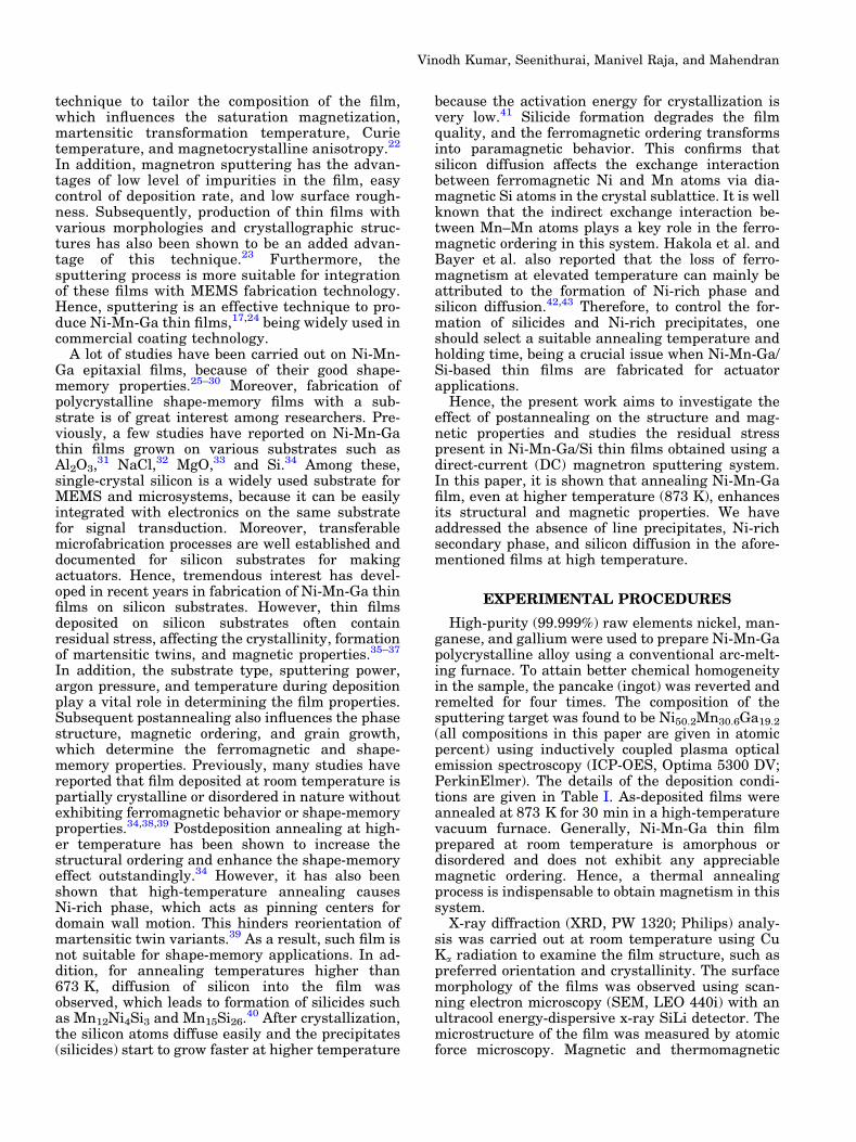
The XRD pattern of as-deposited Ni-Mn-Ga thinfilm is depicted in Fig. 1. Two broad peaks centeredaround 43.4� and 85�, in addition to the Si (100)substrate peak, are observed, being attributed to thehigh-temperature austenite cubic phase. The broadnature of the peaks reveals that the thin films arequasi-amorphous.34,44 After heat treatment at873 K for 30 min, crystallization is clearly detectedin the film (Fig. 2). The diffraction peaks areindexed as the Heusler-type cubic structure (220),(311), (313), and (422). In general, the XRD patterncorresponding to the L21 structure should have twotypes of superstructure diffraction lines, in additionto the fundamental reflections. In the annealed film,the superlattice peaks (200) and (311), along withthe fundamental peaks (220) and (422), are clearlyobserved, suggesting the existence of L21 cubicstructure. The lattice constant for the annealed film
was calculated to be 0.5839 nm from Bragg’sequation using the (220) peak, in agreement withpreviously reported lattice constant values corre-sponding to bulk alloy (L21 structure, a =0.5811 nm) and thin film.45,46 Using a Gaussianexpression, the (220) peak was fit to calculate thefull-width at half-maximum (FWHM), yielding anaverage crystallite size of 23.341 nm for the (220)lattice plane. The relatively strong peak at 2h = 70�corresponds to Si (004) plane, and the weak peakaround 2h = 33� is attributed to Si (200). Thesepeaks can be attributed to multiple diffraction bythe silicon wafer oriented in (100) plane.47 In addi-tion, the extra peaks at 2h = 40� and 2h = 60� aredue to manganese oxide (MnO). These MnO peaksare present irrespective of the heat treatmentmethod applied.48,49 However, the color of the filmdid not change after annealing, revealing that theoxidation of the film in the ultrahigh-purity Arenvironment may be insignificant. This implies nochange in the composition of the film after the heattreatment. A similar observation was also made forsputtered Ni-Mn-Ga film.34 In conclusion, the XRDpattern for the film annealed at 873 K for 30 mindoes not show any silicide signal. This implies thatformation of silicides and Ni-rich phase does notoccur in the film annealed at higher temperature.Hence, this annealing temperature and time arewell suited for obtaining good crystallinity andmagnetic ordering in Ni-Mn-Ga thin film.
In general, stress is generated in thin films due to anumber of factors such as recrystallization, variation ofinteratomic spacing with grain size, microscopic voids,stress relaxation, thermal and lattice misfit, and phasetransformation.37,50,51 The position of the (220) funda-mental reflection peak (Figs. 1 and 2) shifted towardshigher 2h value, indicating a decrease in interatomicspacing. Therefore, the compressive stress present inthe film is due to the variation of interatomic spacing.50
Table I. Preparation details of Ni-Mn-Ga thin filmusing DC magnetron sputtering system
Substrate Si (100)Sputtering power (W) 100Sputtering voltage (V) 367Sputtering current (A) 0.265Sputtering pressure (mTorr) 10Target–substrate distance (cm) 10Thickness (nm) 500 ± 5Growth rate (nm/s) 0.208
Fig. 1. XRD pattern of as-deposited Ni-Mn-Ga film grown at roomtemperature on Si (100) substrate.
Fig. 2. XRD pattern of Ni-Mn-Ga film grown at room temperatureand annealed at 873 K for 30 min.
Structural and Magnetic Properties of Sputter-Deposited Polycrystalline Ni-Mn-GaFerromagnetic Shape-Memory Thin Films
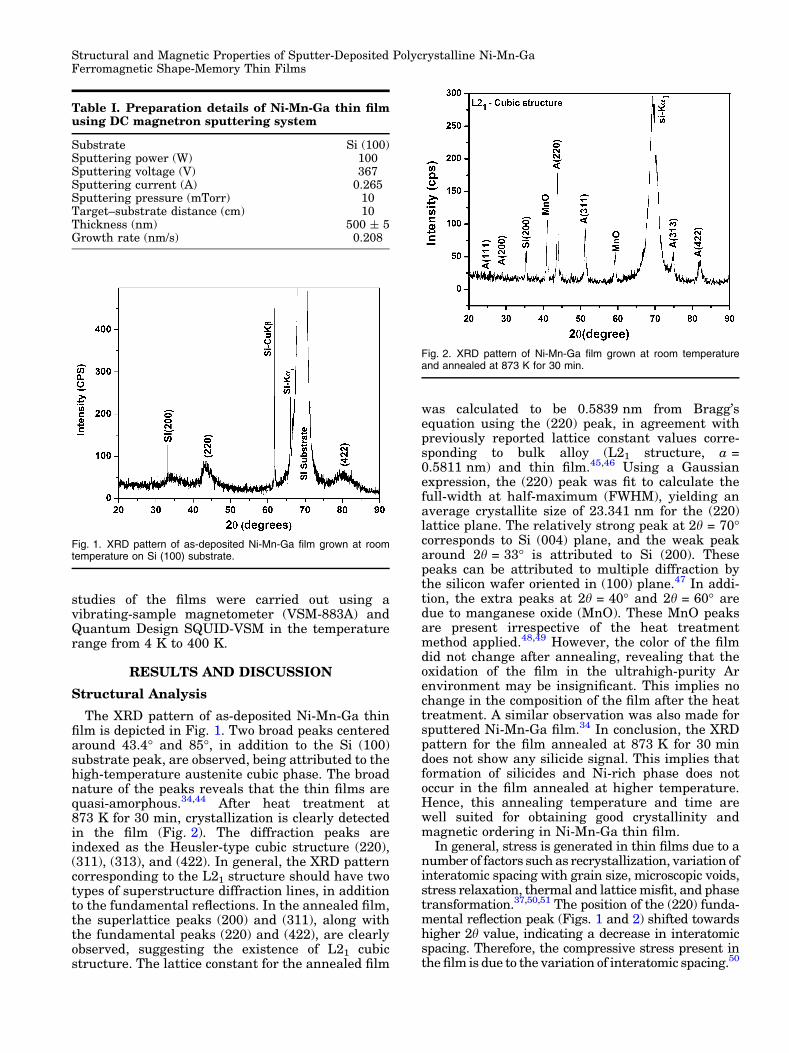
Atom pinning in the lattice during film deposition athigher sputtering power causes compressive stress inthefilm,asreported inthe literature.37 TheFWHMandintensity of the peaks differed for the annealed filmcompared with the as-deposited film. These resultsreveal that the internal stress of the film is releasedafterannealing.Themicrostrainof theannealedfilmascalculated from the Williamson–Hall plot (Fig. 3) wasabout 0.4583.
Microstructure Analysis
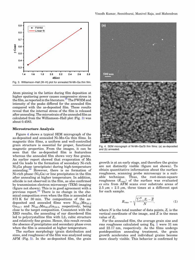
Figure 4 shows a typical SEM micrograph of theas-deposited and annealed Ni-Mn-Ga thin films. Inmagnetic thin films, a uniform and well-controlledgrain structure is essential for proper, functionalmagnetic properties. From the images, it can beseen that the as-deposited film is featurelesswhereas the annealed film shows very fine grains.An earlier report showed that evaporation of Mnand Ga leads to the formation of secondary Ni-richNi3Ga phase (precipitate) during high-temperatureannealing.39 However, there is no formation ofNi-rich phase (Ni3Ga) or line precipitates in the filmafter annealing at higher temperature. In addition,silicide is not observed in the film, as also confirmedby transmission electron microscopy (TEM) imaging(figure not shown). This is in good agreement with aprevious report.52 There is no change in the che-mical composition even when the film is annealed at873 K for 30 min. The compositions of the as-deposited and annealed films were Ni50.1Mn30.2
Ga19.7 and Ni49.7Mn30.8Ga19.5, respectively, beingclose to the target composition. Consistent with theXRD results, the annealing of our disordered filmled to polycrystalline film with L21 cubic structureand relatively fine grains. Hence, this result revealsthe absence of precipitates and secondary phase evenwhen the film is annealed at higher temperature.
The surface morphology (grain distribution andsizes, and roughness) of the film was analyzed usingAFM (Fig. 5). In the as-deposited film, the grain
growth is at an early stage, and therefore the grainsare not distinctly visible (figure not shown). Toobtain quantitative information about the surfaceroughness, scanning probe microscopy is a suit-able technique. Thus, the root-mean-squareroughness (Rrms) of the surface was evaluatedex situ from AFM scans over substrate areas of2.5 lm 9 2.5 lm, three times at a different spotfor each sample.
Rrms ¼
ffiffiffiffiffiffiffiffiffiffiffiffiffiffiffiffiffiffiffiffiffiffiffiffiffiffi
PNi¼1 Zi � Z
N
s
; (1)
where N is the total number of data points, Zi is thevertical coordinate of the image, and Z is the meanvalue of Zi.
For the annealed film, the average grain size andrms roughness calculated using Eq. 1 were 31 nmand 22.17 nm, respectively. As the films undergopostdeposition annealing treatment, the graingrowth accelerates and individual grains becomemore clearly visible. This behavior is confirmed by
Fig. 3. Williamson–Hall (W–H) plot for annealed Ni-Mn-Ga thin film.
Fig. 4. SEM micrograph of Ni-Mn-Ga/Si thin films: (a) as-depositedand (b) annealed.
Vinodh Kumar, Seenithurai, Manivel Raja, and Mahendran
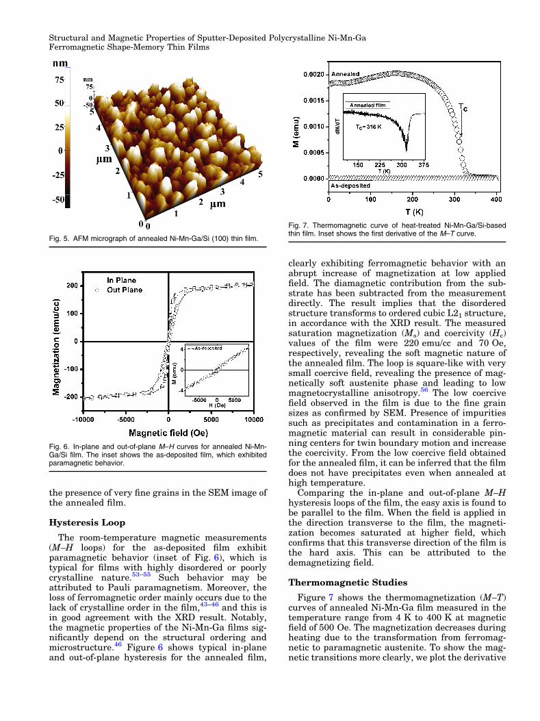
the presence of very fine grains in the SEM image ofthe annealed film.
Hysteresis Loop
The room-temperature magnetic measurements(M–H loops) for the as-deposited film exhibitparamagnetic behavior (inset of Fig. 6), which istypical for films with highly disordered or poorlycrystalline nature.53–55 Such behavior may beattributed to Pauli paramagnetism. Moreover, theloss of ferromagnetic order mainly occurs due to thelack of crystalline order in the film,43–46 and this isin good agreement with the XRD result. Notably,the magnetic properties of the Ni-Mn-Ga films sig-nificantly depend on the structural ordering andmicrostructure.46 Figure 6 shows typical in-planeand out-of-plane hysteresis for the annealed film,
clearly exhibiting ferromagnetic behavior with anabrupt increase of magnetization at low appliedfield. The diamagnetic contribution from the sub-strate has been subtracted from the measurementdirectly. The result implies that the disorderedstructure transforms to ordered cubic L21 structure,in accordance with the XRD result. The measuredsaturation magnetization (Ms) and coercivity (Hc)values of the film were 220 emu/cc and 70 Oe,respectively, revealing the soft magnetic nature ofthe annealed film. The loop is square-like with verysmall coercive field, revealing the presence of mag-netically soft austenite phase and leading to lowmagnetocrystalline anisotropy.56 The low coercivefield observed in the film is due to the fine grainsizes as confirmed by SEM. Presence of impuritiessuch as precipitates and contamination in a ferro-magnetic material can result in considerable pin-ning centers for twin boundary motion and increasethe coercivity. From the low coercive field obtainedfor the annealed film, it can be inferred that the filmdoes not have precipitates even when annealed athigh temperature.
Comparing the in-plane and out-of-plane M–Hhysteresis loops of the film, the easy axis is found tobe parallel to the film. When the field is applied inthe direction transverse to the film, the magneti-zation becomes saturated at higher field, whichconfirms that this transverse direction of the film isthe hard axis. This can be attributed to thedemagnetizing field.
Thermomagnetic Studies
Figure 7 shows the thermomagnetization (M–T)curves of annealed Ni-Mn-Ga film measured in thetemperature range from 4 K to 400 K at magneticfield of 500 Oe. The magnetization decreases duringheating due to the transformation from ferromag-netic to paramagnetic austenite. To show the mag-netic transitions more clearly, we plot the derivative
Fig. 5. AFM micrograph of annealed Ni-Mn-Ga/Si (100) thin film.
Fig. 6. In-plane and out-of-plane M–H curves for annealed Ni-Mn-Ga/Si film. The inset shows the as-deposited film, which exhibitedparamagnetic behavior.
Fig. 7. Thermomagnetic curve of heat-treated Ni-Mn-Ga/Si-basedthin film. Inset shows the first derivative of the M–T curve.
Structural and Magnetic Properties of Sputter-Deposited Polycrystalline Ni-Mn-GaFerromagnetic Shape-Memory Thin Films
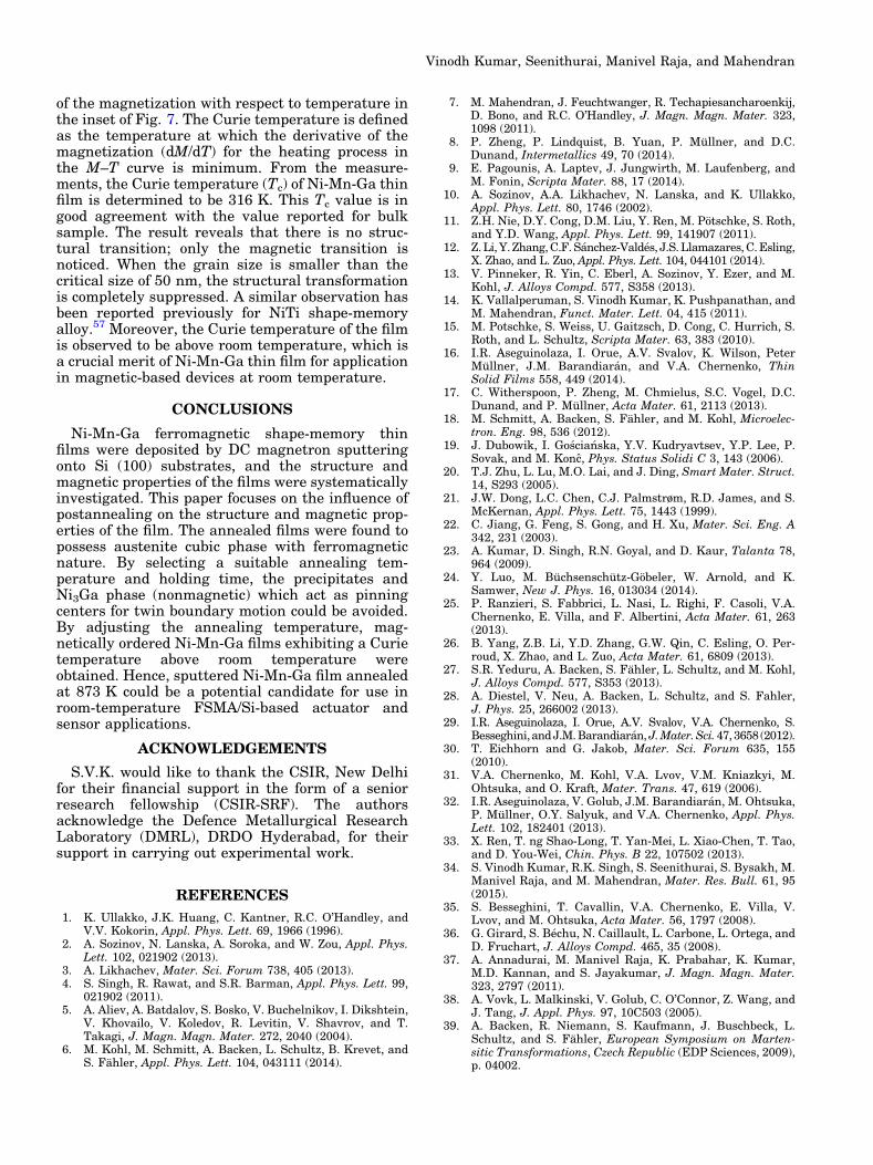
of the magnetization with respect to temperature inthe inset of Fig. 7. The Curie temperature is definedas the temperature at which the derivative of themagnetization (dM/dT) for the heating process inthe M–T curve is minimum. From the measure-ments, the Curie temperature (Tc) of Ni-Mn-Ga thinfilm is determined to be 316 K. This Tc value is ingood agreement with the value reported for bulksample. The result reveals that there is no struc-tural transition; only the magnetic transition isnoticed. When the grain size is smaller than thecritical size of 50 nm, the structural transformationis completely suppressed. A similar observation hasbeen reported previously for NiTi shape-memoryalloy.57 Moreover, the Curie temperature of the filmis observed to be above room temperature, which isa crucial merit of Ni-Mn-Ga thin film for applicationin magnetic-based devices at room temperature.
CONCLUSIONS
Ni-Mn-Ga ferromagnetic shape-memory thinfilms were deposited by DC magnetron sputteringonto Si (100) substrates, and the structure andmagnetic properties of the films were systematicallyinvestigated. This paper focuses on the influence ofpostannealing on the structure and magnetic prop-erties of the film. The annealed films were found topossess austenite cubic phase with ferromagneticnature. By selecting a suitable annealing tem-perature and holding time, the precipitates andNi3Ga phase (nonmagnetic) which act as pinningcenters for twin boundary motion could be avoided.By adjusting the annealing temperature, mag-netically ordered Ni-Mn-Ga films exhibiting a Curietemperature above room temperature wereobtained. Hence, sputtered Ni-Mn-Ga film annealedat 873 K could be a potential candidate for use inroom-temperature FSMA/Si-based actuator andsensor applications.
ACKNOWLEDGEMENTS
S.V.K. would like to thank the CSIR, New Delhifor their financial support in the form of a seniorresearch fellowship (CSIR-SRF). The authorsacknowledge the Defence Metallurgical ResearchLaboratory (DMRL), DRDO Hyderabad, for theirsupport in carrying out experimental work.
REFERENCES
1. K. Ullakko, J.K. Huang, C. Kantner, R.C. O’Handley, andV.V. Kokorin, Appl. Phys. Lett. 69, 1966 (1996).
2. A. Sozinov, N. Lanska, A. Soroka, and W. Zou, Appl. Phys.Lett. 102, 021902 (2013).
3. A. Likhachev, Mater. Sci. Forum 738, 405 (2013).4. S. Singh, R. Rawat, and S.R. Barman, Appl. Phys. Lett. 99,
021902 (2011).5. A. Aliev, A. Batdalov, S. Bosko, V. Buchelnikov, I. Dikshtein,
V. Khovailo, V. Koledov, R. Levitin, V. Shavrov, and T.Takagi, J. Magn. Magn. Mater. 272, 2040 (2004).
6. M. Kohl, M. Schmitt, A. Backen, L. Schultz, B. Krevet, andS. Fahler, Appl. Phys. Lett. 104, 043111 (2014).
7. M. Mahendran, J. Feuchtwanger, R. Techapiesancharoenkij,D. Bono, and R.C. O’Handley, J. Magn. Magn. Mater. 323,1098 (2011).
8. P. Zheng, P. Lindquist, B. Yuan, P. Mullner, and D.C.Dunand, Intermetallics 49, 70 (2014).
9. E. Pagounis, A. Laptev, J. Jungwirth, M. Laufenberg, andM. Fonin, Scripta Mater. 88, 17 (2014).
10. A. Sozinov, A.A. Likhachev, N. Lanska, and K. Ullakko,Appl. Phys. Lett. 80, 1746 (2002).
11. Z.H. Nie, D.Y. Cong, D.M. Liu, Y. Ren, M. Potschke, S. Roth,and Y.D. Wang, Appl. Phys. Lett. 99, 141907 (2011).
12. Z. Li, Y. Zhang, C.F. Sanchez-Valdes, J.S. Llamazares, C. Esling,X. Zhao, and L. Zuo, Appl. Phys. Lett. 104, 044101 (2014).
13. V. Pinneker, R. Yin, C. Eberl, A. Sozinov, Y. Ezer, and M.Kohl, J. Alloys Compd. 577, S358 (2013).
14. K. Vallalperuman, S. Vinodh Kumar, K. Pushpanathan, andM. Mahendran, Funct. Mater. Lett. 04, 415 (2011).
15. M. Potschke, S. Weiss, U. Gaitzsch, D. Cong, C. Hurrich, S.Roth, and L. Schultz, Scripta Mater. 63, 383 (2010).
16. I.R. Aseguinolaza, I. Orue, A.V. Svalov, K. Wilson, PeterMullner, J.M. Barandiaran, and V.A. Chernenko, ThinSolid Films 558, 449 (2014).
17. C. Witherspoon, P. Zheng, M. Chmielus, S.C. Vogel, D.C.Dunand, and P. Mullner, Acta Mater. 61, 2113 (2013).
18. M. Schmitt, A. Backen, S. Fahler, and M. Kohl, Microelec-tron. Eng. 98, 536 (2012).
19. J. Dubowik, I. Goscianska, Y.V. Kudryavtsev, Y.P. Lee, P.Sovak, and M. Konc, Phys. Status Solidi C 3, 143 (2006).
20. T.J. Zhu, L. Lu, M.O. Lai, and J. Ding, Smart Mater. Struct.14, S293 (2005).
21. J.W. Dong, L.C. Chen, C.J. Palmstrøm, R.D. James, and S.McKernan, Appl. Phys. Lett. 75, 1443 (1999).
22. C. Jiang, G. Feng, S. Gong, and H. Xu, Mater. Sci. Eng. A342, 231 (2003).
23. A. Kumar, D. Singh, R.N. Goyal, and D. Kaur, Talanta 78,964 (2009).
24. Y. Luo, M. Buchsenschutz-Gobeler, W. Arnold, and K.Samwer, New J. Phys. 16, 013034 (2014).
25. P. Ranzieri, S. Fabbrici, L. Nasi, L. Righi, F. Casoli, V.A.Chernenko, E. Villa, and F. Albertini, Acta Mater. 61, 263(2013).
26. B. Yang, Z.B. Li, Y.D. Zhang, G.W. Qin, C. Esling, O. Per-roud, X. Zhao, and L. Zuo, Acta Mater. 61, 6809 (2013).
27. S.R. Yeduru, A. Backen, S. Fahler, L. Schultz, and M. Kohl,J. Alloys Compd. 577, S353 (2013).
28. A. Diestel, V. Neu, A. Backen, L. Schultz, and S. Fahler,J. Phys. 25, 266002 (2013).
29. I.R. Aseguinolaza, I. Orue, A.V. Svalov, V.A. Chernenko, S.Besseghini,andJ.M.Barandiaran,J.Mater.Sci.47,3658 (2012).
30. T. Eichhorn and G. Jakob, Mater. Sci. Forum 635, 155(2010).
31. V.A. Chernenko, M. Kohl, V.A. Lvov, V.M. Kniazkyi, M.Ohtsuka, and O. Kraft, Mater. Trans. 47, 619 (2006).
32. I.R. Aseguinolaza, V. Golub, J.M. Barandiaran, M. Ohtsuka,P. Mullner, O.Y. Salyuk, and V.A. Chernenko, Appl. Phys.Lett. 102, 182401 (2013).
33. X. Ren, T. ng Shao-Long, T. Yan-Mei, L. Xiao-Chen, T. Tao,and D. You-Wei, Chin. Phys. B 22, 107502 (2013).
34. S. Vinodh Kumar, R.K. Singh, S. Seenithurai, S. Bysakh, M.Manivel Raja, and M. Mahendran, Mater. Res. Bull. 61, 95(2015).
35. S. Besseghini, T. Cavallin, V.A. Chernenko, E. Villa, V.Lvov, and M. Ohtsuka, Acta Mater. 56, 1797 (2008).
36. G. Girard, S. Bechu, N. Caillault, L. Carbone, L. Ortega, andD. Fruchart, J. Alloys Compd. 465, 35 (2008).
37. A. Annadurai, M. Manivel Raja, K. Prabahar, K. Kumar,M.D. Kannan, and S. Jayakumar, J. Magn. Magn. Mater.323, 2797 (2011).
38. A. Vovk, L. Malkinski, V. Golub, C. O’Connor, Z. Wang, andJ. Tang, J. Appl. Phys. 97, 10C503 (2005).
39. A. Backen, R. Niemann, S. Kaufmann, J. Buschbeck, L.Schultz, and S. Fahler, European Symposium on Marten-sitic Transformations, Czech Republic (EDP Sciences, 2009),p. 04002.
Vinodh Kumar, Seenithurai, Manivel Raja, and Mahendran
40. J.P. Ahn, N. Cheng, T. Lograsso, and K.M. Krishnan, IEEETrans. Magn. 37, 2141 (2001).
41. Y.Q. Yang, H.S. Jia, Z.F. Zhang, H.M. Shen, A. Hu, and Y.N.Wang, Mater. Lett. 22, 137 (1995).
42. A. Hakola, O. Heczko, A. Jaakkola, T. Kajava, and K.Ullakko, Appl. Phys. A 79, 1505 (2004).
43. B.C. Bayer, A.F. Khan, M. Mehmood, and Z.H. Barber, ThinSolid Films 518, 2659 (2010).
44. S.K. Wu, K.H. Tseng, and J.Y. Wang, Thin Solid Films 408,316 (2002).
45. Z. Li, B. Yang, Y. Zhang, C. Esling, N. Zou, X. Zhao, and L.Zuo, Acta Mater. 74, 9 (2014).
46. J.Y. Rhee, Y.V. Kudryavtsev, J. Dubowik, and Y.P. Lee,J. Appl. Phys. 93, 5527 (2003).
47. B.-H. Hwang, J. Phys. D Appl. Phys. 34, 2469 (2001).48. M. Suzuki, M. Ohtsuka, M. Matsumoto, Y. Murakami, D.
Shindo, and K. Itagaki, Mater. Trans. 43, 861 (2002).
49. A. Gebert, S. Roth, S. Oswald, and L. Schultz, Corros. Sci.51, 1163 (2009).
50. W.D. Nix and B.M. Clemens, J. Mater. Res. 14, 3467 (1999).51. W. Buckel, J. Vac. Sci. Technol. 6, 606 (1969).52. F. Bernard, C. Rousselot, L. Hirsinger, and P. Delobelle,
Eur. Phys. J. Spec. Top. 158, 187 (2008).53. F. Bernard, P. Delobelle, C. Rousselot, and L. Hirsinger,
Thin Solid Films 518, 399 (2009).54. H. Rumpf, C.M. Craciunescu, H. Modrow, K. Olimov, E.
Quandt, and M. Wuttig,J.Magn.Magn.Mater.302, 421 (2006).55. F.J. Castano, B. Nelson-Cheeseman, R.C. O’Handley, C.A.
Ross, C. Redondo, and F. Castano, J. Appl. Phys. 93, 8492(2003).
56. R. Tickle and R.D. James, J. Magn. Magn. Mater. 195, 627(1999).
57. T. Waitz, T. Antretter, F.D. Fischer, and H.P. Karnthaler,Mater. Sci. Technol. 24, 934 (2008).
Structural and Magnetic Properties of Sputter-Deposited Polycrystalline Ni-Mn-GaFerromagnetic Shape-Memory Thin Films
Copyright © 2022 FDOKUMEN