visible light modulation using chemically deposited ...
6
ISSN 2466-4294 (online) | rad-journal.org Vol. 2 | Issue 1 | pp. 35 – 40 doi: 10.21175/RadJ.2017.01.008 Original research paper VISIBLE LIGHT MODULATION USING CHEMICALLY DEPOSITED ELECTROCHROMIC THIN FILMS * Julijana Velevska 1** , Nace Stojanov 1 , Margareta Pecovska-Gjorgjevich 1 , Metodija Najdoski 2 1 Institute of Physics, Faculty of Natural Sciences and Mathematics, Sts Cyril and Methodius University, Skopje, Republic of Macedonia 2 Institute of Chemistry, Faculty of Natural Sciences and Mathematics, Sts Cyril and Methodius University, Skopje, Republic of Macedonia Abstract. In this work, electrochromic Prussian blue (PB) and tungsten oxide (WO3) thin films have been prepared by the chemical bath deposition method. The films have been deposited onto fluorine doped tin oxide (FTO) coated glass substrates. Electrochromic behavior of each film was studied by cyclic voltammetry. An electrochromic test device (ECTD) was constructed by using WO3 as a working electrode, together with a PB film as an opposite (counter) electrode, and aqueous solution of 1 mol/dm 3 KCl, slightly acidified with 2 drops of conc. HCl in 100 ml, as an electrolyte. The optical transmission spectra of the bleached and colored states were recorded in the visible part of the spectrum. The contrast ratio was calculated from these spectra. The coloration efficiency and the time response of the ECTD were also examined. Key words: Electrochromism, chemical bath deposition, thin film * The paper was presented at the Fourth International Conference on Radiation and Applications in Various Fields of Research (RAD 2016), Niš, Serbia, 2016. ** [email protected] & [email protected] 1. INTRODUCTION The last few years we are witnesses of gradual increase in the environmental problems. Global warming due to the increasing of carbon dioxide emission has been one of the major problems that appeared and threatened our environment in many aspects. Since environment protection is now an unavoidable subject, it has become a priority to reduce our energy consumption. Perhaps it sounds incredible, but buildings, consuming more than one third of the overall energy worldwide, have more impact on environment than industry and transportation. This is the reason why, the energy consumption reduction in the buildings is a big challenge for every country in the world. Over the last years, building design has been oriented toward the optimization of energy usage, the protection of the environment and the occupants’ comfort [1]. On the other hand, modern urban architecture involves the construction of large buildings with a big percentage of glazed areas. Since glazing constitutes one of the less energy efficient components of the building envelope, the reduction of building energy consumption becomes an important challenge not only for the architects and civil engineers, but also for the scientists. Control of the energy transfer through windows is very important in connection with reduction in energy consumption. The poor energy efficiency of glazing compared to the other components of the building envelope offers great opportunities to develop new glazing technologies that are more energy efficient. Electrochromic glazing (i.e. smart windows) is a new technology which has the potential to transform the way we use glass in buildings [2]. Crucial role in electrochromic windows have special materials that have electrochromic properties. “Electrochromic” describes materials that can change their optical properties (color) by applying a small voltage. When thin films of such materials are integrated in devices, it becomes possible to modulate the transmittance, absorptance, reflectance and emittance between widely separated extrema [3]-[5]. A standard electrochromic design consists of a substrate coated with a transparent conductor, the electrochromic film, an electrolyte, a film serving as ion storage (ideally with electrochromic properties complementary to those of the first electrochromic film), another transparent conductor and a substrate. When a small voltage is applied between the transparent conductors, ions are forced to transfer from the ion storage film, through the electrolyte, to the electrochromic film. At the same time the electrons are injected into the electrochromic film from the substrate. The electrons are needed to preserve charge neutrality. Optical properties are altered as an effect of injection of electrons into the electrochromic film. Reversing the voltage polarity brings back the original properties [6]. The electrochromic material is the optically active material in the electrochromic device. It is deposited on
-
Upload
khangminh22 -
Category
Documents
-
view
3 -
download
0
Transcript of visible light modulation using chemically deposited ...

ISSN 2466-4294 (online) | rad-journal.org
Vol. 2 | Issue 1 | pp. 35 – 40 doi: 10.21175/RadJ.2017.01.008
Original research paper
VISIBLE LIGHT MODULATION USING CHEMICALLY DEPOSITED ELECTROCHROMIC THIN FILMS*
Julijana Velevska1**, Nace Stojanov1, Margareta Pecovska-Gjorgjevich1, Metodija Najdoski2
1Institute of Physics, Faculty of Natural Sciences and Mathematics, Sts Cyril and Methodius University, Skopje, Republic of Macedonia
2Institute of Chemistry, Faculty of Natural Sciences and Mathematics, Sts Cyril and Methodius University, Skopje, Republic of Macedonia
Abstract. In this work, electrochromic Prussian blue (PB) and tungsten oxide (WO3) thin films have been prepared by the chemical bath deposition method. The films have been deposited onto fluorine doped tin oxide (FTO) coated glass substrates. Electrochromic behavior of each film was studied by cyclic voltammetry. An electrochromic test device (ECTD) was constructed by using WO3 as a working electrode, together with a PB film as an opposite (counter) electrode, and aqueous solution of 1 mol/dm3 KCl, slightly acidified with 2 drops of conc. HCl in 100 ml, as an electrolyte. The optical transmission spectra of the bleached and colored states were recorded in the visible part of the spectrum. The contrast ratio was calculated from these spectra. The coloration efficiency and the time response of the ECTD were also examined.
Key words: Electrochromism, chemical bath deposition, thin film
* The paper was presented at the Fourth International Conference on Radiation and Applications in Various Fields of Research (RAD 2016), Niš, Serbia, 2016. ** [email protected] & [email protected]
1. INTRODUCTION
The last few years we are witnesses of gradual increase in the environmental problems. Global warming due to the increasing of carbon dioxide emission has been one of the major problems that appeared and threatened our environment in many aspects. Since environment protection is now an unavoidable subject, it has become a priority to reduce our energy consumption. Perhaps it sounds incredible, but buildings, consuming more than one third of the overall energy worldwide, have more impact on environment than industry and transportation. This is the reason why, the energy consumption reduction in the buildings is a big challenge for every country in the world.
Over the last years, building design has been oriented toward the optimization of energy usage, the protection of the environment and the occupants’ comfort [1]. On the other hand, modern urban architecture involves the construction of large buildings with a big percentage of glazed areas. Since glazing constitutes one of the less energy efficient components of the building envelope, the reduction of building energy consumption becomes an important challenge not only for the architects and civil engineers, but also for the scientists. Control of the energy transfer through windows is very important in connection with reduction in energy consumption. The poor energy efficiency of glazing compared to the other
components of the building envelope offers great opportunities to develop new glazing technologies that are more energy efficient.
Electrochromic glazing (i.e. smart windows) is a new technology which has the potential to transform the way we use glass in buildings [2]. Crucial role in electrochromic windows have special materials that have electrochromic properties. “Electrochromic” describes materials that can change their optical properties (color) by applying a small voltage. When thin films of such materials are integrated in devices, it becomes possible to modulate the transmittance, absorptance, reflectance and emittance between widely separated extrema [3]-[5]. A standard electrochromic design consists of a substrate coated with a transparent conductor, the electrochromic film, an electrolyte, a film serving as ion storage (ideally with electrochromic properties complementary to those of the first electrochromic film), another transparent conductor and a substrate. When a small voltage is applied between the transparent conductors, ions are forced to transfer from the ion storage film, through the electrolyte, to the electrochromic film. At the same time the electrons are injected into the electrochromic film from the substrate. The electrons are needed to preserve charge neutrality. Optical properties are altered as an effect of injection of electrons into the electrochromic film. Reversing the voltage polarity brings back the original properties [6].
The electrochromic material is the optically active material in the electrochromic device. It is deposited on
J. Velevska et al., Visible Light Modulation..., Rad. Applic., 2017, 2, 1, 35–40
36
top of the transparent conductor. There are a number of methods to produce the electrochromic materials in the form of thin film [3]. Electrochromic properties of the films strongly depend on the preparation method, which means that the films of same material prepared by different method have different electrochromic properties.
Among the vast number of thin film deposition methods, chemical bath deposition has many advantages: it does not require sophisticated equipment like vacuum system and other expensive instruments, the starting chemicals are commonly available and cheap, various substrates including insulators, semiconductors or metals can be used, and the preparation parameters are easily controlled [7]-[11].
This paper presents investigations of visible light modulation using electrochromic test device (ECTD) with complementary electrochromic films prepared by chemical bath deposition method.
2. MATERIALS AND METHODS
Tungsten oxide (WO3) and Prussian blue [PB, iron(III) hexacyanoferrate(II)] electrochromic thin films have been deposited onto fluorine doped tin oxide (FTO) coated glass substrates commercially available, with transparency of about 80% for visible light and sheet resistance of about 15 Ω/□. Electric resistivity and transmittance are the most important properties for the transparent conducting layers (FTO) in electrochromic applications. The layers should have high electronic conductivity because the electric field needed for electrochromic devices to work is applied between these conducting layers. The electrical properties of the FTO layers affect the responsiveness of the electrochromic devices. On the other hand, these layers should not affect the transmittance.
2.1. Deposition of tungsten oxide thin films
The deposition of the WO3 thin films was performed from one solution prepared of 1.65 g Na2WO4·2H2O dissolved in 90 ml deionized water [9]. The substrates were vertically supported against the walls of the beaker. Then, the whole system was heated slowly, up to 950 C with continuous stirring. The deposition time was 20 min. The thickness of the films, measured by Dectak Stylus Profilometer, was 150 nm.
2.2. Deposition of Prussian blue thin films
PB thin films were deposited from two solutions. One of the solutions was prepared by mixing of 15 ml 0.1 mol/dm3 Fe2(SO4)3, 90 ml H2O, 0.5 g EDTA (Ethylenediaminetetraacetic acid) and 10 ml 3 mol/dm3 HCl, while the second solution was an aqueous solution of 15 ml 0.1 mol/dm3 K4[Fe(CN)6], 90 ml H2O and 10 ml 3 mol/dm3 HCl. Before the deposition, the solutions were heated up to 600 C. The films were produced by successive immersion of the substrates into the solutions [11]. The thickness of the films depends on the number of immersion cycles. In this work PB films were deposited by 20 cycles, which results with 140 nm thick films.
2.3. Characterization
The electrochromic behavior of WOx and PB thin films was examined by cyclic voltammetry (CV) which was performed using Micro AUTOLAB II equipment (Eco-Chemie Utrecht Netherlands). A saturated calomel electrode (SCE) and a platinum wire were used as a reference and counter electrodes respectively. The cycling was carried out in 1 mol/dm3 KCl aqueous solution, slightly acidified with 2 drops of conc. HCl in 100 ml of the solution, as an electrolyte. The voltage scan rate was 10mV/s, and the film working area was 1cm2.
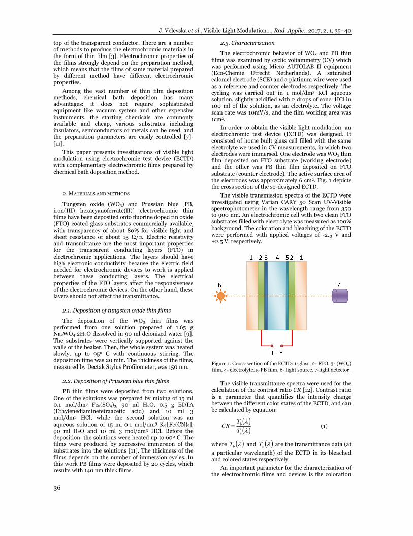
In order to obtain the visible light modulation, an electrochromic test device (ECTD) was designed. It consisted of home built glass cell filled with the same electrolyte we used in CV measurements, in which two electrodes were immersed. One electrode was WO3 thin film deposited on FTO substrate (working electrode) and the other was PB thin film deposited on FTO substrate (counter electrode). The active surface area of the electrodes was approximately 6 cm2. Fig. 1 depicts the cross section of the so-designed ECTD.
The visible transmission spectra of the ECTD were investigated using Varian CARY 50 Scan UV-Visible spectrophotometer in the wavelength range from 350 to 900 nm. An electrochromic cell with two clean FTO substrates filled with electrolyte was measured as 100% background. The coloration and bleaching of the ECTD were performed with applied voltages of -2.5 V and +2.5 V, respectively.
Figure 1. Cross-section of the ECTD: 1-glass, 2- FTO, 3- (WOx) film, 4- electrolyte, 5-PB film, 6- light source, 7-light detector.
The visible transmittance spectra were used for the calculation of the contrast ratio CR [12]. Contrast ratio is a parameter that quantifies the intensity change between the different color states of the ECTD, and can be calculated by equation:
c
b
T
TCR (1)
where bT and cT are the transmittance data (at
a particular wavelength) of the ECTD in its bleached and colored states respectively.
An important parameter for the characterization of the electrochromic films and devices is the coloration

J. Velevska et al., Visible Light Modulation..., Rad. Applic., 2017, 2, 1, 35–40
37
efficiency which represents the change in the
optical density OD per unit charge density change ΔQ/A during coloration [13] and can be calculated by the equation:
Q
TTA cb
log (2)
where bT and cT are the transmittance data of the
bleached and colored states respectively, ΔQ is the change of the injected/ejected charge determined by the applied current through the ECTD and the time of its application, and A is the active electrode area. It can be shown that the overall coloration efficiency of the complementary electrochromic system is the sum of the coloration efficiencies of the individual coloring films. That is, the overall coloration efficiency is the sum of coloration efficiency of the working electrode-
w , and that of the counter electrode- c , or:
c
cb
w
cb
cw
Q
TTA
Q
TTA
loglog
(3)
The time taken for an electrochromic material or device to switch between its colored and bleached states is known as response time. The responsiveness of the ECTD was examined at 550 nm (white light) as a transmittance change due to the abrupt voltage change between -2.5 and +2.5 V.
3. RESULTS AND DISCUSSION
Chemically deposited WO3 and PB thin films investigated in this work exhibited good electrochromic properties. They could be repeatedly colored and bleached with the alternative application of a negative and positive potential. WO3 is cathodically coloring material, which means that it possess a reduced colored state, while PB is anodically coloring material with oxidized colored state.
The cyclic voltammograms (CV) for the WO3 film were obtained by sweeping the potential in the range of -0.8 to 0 V vs. SCE at scanning rate of 10 mV/s (Fig. 2). From CV curves one can observe an increase of the cathodic current density to -0.86 mA/cm2 at -0.8 V, due to the reduction process occurring in the film, and its switch to the blue color, whereas at -0.54 V anodic peak is observed and is due to the oxidation process and bleaching of the film [14]. The coloring/ bleaching process is in direct relation with intercalation and deintercalation of potassium ions expressed by the following equation:
colored
ttransparen
3x
-3
WOK
xexKWO
(3a)
-
3
3x
xexKWO
WOK
ttransparen
colored
(3b)
Figure 2. Cyclic voltammograms (five cycles) at 10 mV/s scan rate for chemically deposited WO3 film in 1moll/dm3 KCl
aqueous solution. Arrows indicate direction of the potential scan
Figure 3. Cyclic voltammograms (five cycles) at 10 mV/s scan
rate for chemically deposited PB films in 1moll/dm3 KCl aqueous solution. Arrows indicate direction of the
potential scan
The cyclic voltammograms for the PB film, depicted in Fig. 3 and recorded at a scanning rate of 10 mV/s, were obtained by sweeping the potential in the range of -0.8 to +0.6 V vs. SCE. It can be seen that CV curves show two sharp peaks. The oxidation peak at 0.21 V and the reduction peak at 0.18 V are due to the coloring and bleaching processes respectively. Bleaching process is followed by reduction of FeIII ions and intercalation of potassium ions:
ttransparen
colored
6IIII
2
-6
IIIII
CNFeFeK
eKCNFeKFe
(4a)
The coloration is followed by the opposite process – oxidation of FeII ions and deintercalation of potassium ions:
-
6IIIII
6IIII
2
eKCNFeKFe
CNFeFeK
colored
ttransparen
(4b)
Chemically deposited WO3 and PB electrochromic thin films were used for designing an ECTD (Fig. 1).

J. Velevska et al., Visible Light Modulation..., Rad. Applic., 2017, 2, 1, 35–40
38
This ECTD shows light modulation by applying a DC potential between working (glass/FTO/WO3) and counter (glass/FTO/PB) electrodes. Coloration is achieved by applying -2.5 V of the WO3 side, and reversal potential shows bleaching. When a potential is applied across the two electrodes, potassium ions are shuttled through the electrolyte between the anodic (PB) and the chatodic (WO3) electrochromic film. At the same time, electrons are shuttled to/from the electrochromic films from/to the electronically conductive layers (FTO). When potassium ions and electrons meet in cathodic (WO3) electrochromic film, reduction of WO3 occurs and its color changes from transparent to deep blue as depicted by Eq. (3a), whereas at the same time, oxidation of PB counter electrode occurs due to the extraction of potassium ions and electrons, and its color also changes from transparent to blue as depicted by Eq (4b). As a result, ECTD is blue colored. When potassium ions and electrons meet in anodic (PB) electrochromic film, by changing the polarity of the applied potential, reduction of PB occurs and its color changes from deep blue to transparent as depicted by Eq. (4a), whereas at the same time, due to the extraction of potassium ions and electrons, oxidation of WO3 working electrode occurs and it becomes transparent according with Eq. (3b). As a result, ECTD is bleached. Ion transport occurs between the two electrochromic films via electrolyte. Fig. 4 presents photograph of ECTD in its colored and bleached (transparent) states.
Figure 4. Photographs of ECTD in its colored and bleached
states after application of E=-2.5 V, and E=+2.5 V, respectively
The visible transmission spectra of the ECTD, in the wavelength range from 350 to 900 nm in transparent (bleached) and colored states are presented in Fig. 5. When a positive potential is applied (+2.5 V), ECTD is transparent with transparency of ~70% in the visible range. The application of negative potential (-2.5 V) promotes the color change to blue and a drop of transmittance of the ECTD to less than 10% at the same time.
Figure 6 presents the contrast ratio of the ECTD between the transparent and the colored states, in the wavelength range between 350 and 900 nm, calculated by the equation (1). As can be seen from this Figure, maximum contrast ratio of 9.5 was achieved at 720 nm.
The graphical presentation of the optical density change ΔOD as a function of the charge density change ΔQ/A is depicted in Fig. 7. The coloration efficiency η(λ) at 550 nm (the wavelength at which the human eye is most responsive) was determined as a slope from the linear part of the graph, and it was found to be
71.85 cm2/C. This value is very close to the values reported earlier [15]-[17] for electrochromic devices based on WO3 and PB prepared by different methods and with different electrolyte.
Figure 5. Visible transmittance spectra of ECTD in colored
and bleached states after application of E=-2.5 V, and E=+2.5 V, respectively
Figure 6. Contrast Ratio of the ECTD between its transparent
and colored states
Figure 7. Optical density variation with respect to the charge
density recorded at 550 nm

J. Velevska et al., Visible Light Modulation..., Rad. Applic., 2017, 2, 1, 35–40
39
In order to examine the time response (coloring and bleaching times), the transmittance at 550 nm was measured trough the ECTD (Fig. 8). The applied potential was switched between +2.5 V (bleached state) and -2.5 V (colored state). The bleaching and coloring times, defined as the time to reach 70% of the final change in the transmittance [18], were found to be 7.2 and 2.8 s respectively. It means that the coloring process is faster than bleaching process. It could be explained with the higher resistivity of KxWO3 and KFeIII[FeII(CN)6] (colored state) than WO3 and K2FeII[FeII(CN)6] (bleached state). The similar results were reported in [19] and [20] for WO3 films, and [21] for PB films.
Figure. 8 Switching time characteristics at 550 nm, between
the bleached and colored states for the complementary electrochromic test device measured at ±2.5 V
4. CONCLUSIONS
Electrochromic WO3 and PB thin films were synthesized by chemical bath deposition. The method is simple, economical, and offers a possibility for large area deposition. The chemicals are available and relatively cheap. The obtained films exhibited good electrochromic properties. They were stable and exhibited excellent reversibility. WO3 films were transparent in oxidized and became blue in reduced state (chatodic coloration), while PB films had a blue color in oxidized and became transparent in reduced state (anodic coloration). A complementary ECTD based on chemically deposited WO3 and PB films was fabricated and demonstrates a large difference in the transmittance (63%) and contrast ratio (9.5) at 720 nm, fast switching response (tc=2.8 s and tb=7.2 s) and good coloration efficiency (71.85 cm2C-1) comparable with those reported earlier. Finally we can conclude that chemically deposited WO3 and PB thin films could be very promising materials for applications in electrochromic devices. The complementary device based on these films holds great promise for potential applications in energy-saving smart windows.
REFERENCES
1. J. M. Dussault, L. Gosselin and T. Galtsian, "Assesment of buildings energy efficiency with smart window glazing curtain walls,” in Proc. of Smart materials,
structures & NDT in aerospace, Montreal, Canada, 2011. Retrieved from: http://www.ndt.net/article/ndtcanada2011/papers/12_Dussault_Rev2.pdf Retrieved on: Dec. 12, 2015
2. E. S. Lee, D. L. Di Bartolomeo and S. E. Selkowitz, "Electrochromic windows for commercial buildings: monitored results from a full-scale testbed,” in Proc. of 2000 ACEEE Summer study on Energy Efficiency in Buildings, Panel 3: Comercial Buildings: Technologies, Design and Performance Analysis, 2000. Retrieved from: http://www.eceee.org/library/conference_proceedings/ACEEE_buildings/2000/Panel_3/p3_20/paper Retrieved on: Dec. 12, 2015
3. C. G. Granqvist, Handbook of Inorganic Electrochromic Materials, Amsterdam, The Netherlands: Elsevier, 1995. DOI: 10.1016/B978-044489930-9/50000-3
4. C. G. Granqvist, "Electrochromic tungsten oxide films: Review of progress 1993-1998," Solar Energy Mater. Solar Cells, vol. 60, pp 201-262, 2001. DOI: 10.1016/S0927-0248(99)00088-4
5. C. G. Granqvist, A. Avendano and A. Azens, "Electrochromic coatings and devices: Survay of some recent advances," Thin Solid Films, vol. 442, pp 201-219, 2003. DOI: 10.1016/S0040-6090(03)00983-0
6. S. Arman, "Electrochromic materials for display applications: Introduction," J. New. Mat. Electrochem. Systems, vol. 4, pp 173-179, 2001.
7. M. Ristova, J. Velevska and M. Ristov, "Chemical bath deposition and electrochromic properties of NiOx films," Solar Energy Mater. Solar Cells, vol. 71, pp 219-230, 2002. DOI: 10.1016/S0927-0248(01)00061-7
8. T. Todorovski, M. Najdoski and J. Velevska, "Chemical deposition of molybdenum oxide thin films from dimethyl sulfate bath," International Journal of Pure and Applied Chemistry, vol.1, no. 4, pp 549-552, 2006.
9. M. Najdoski and T. Todorovski, "A simple method for chemical bath deposition of electrochromic tungsten oxide films," Mater. Chem. Phys., vol. 104, no. 2-3, pp 483-487, Aug. 2007. DOI: 10.1016/j.matchemphys.2007.04.035
10. J. Velevska, M. Pecovska-Gjorgjevich, M. Najdoski and N. Stojanov, "Studies on electrochromism of chemically deposited nickel oxide thin films," Silpacorn U Science & Tech J, vol. 5, no. 1, pp 34-42, 2011.
11. S. Demiri, M. Najdoski and J. Velevska, "A simple chemical method for deposition of electrochromic Prussian blue thin films," Mater. Res. Bull., vol. 46, pp 2484-2488, 2011. DOI: 10.1016/j.materresbull.2011.08.021
12. S. A. Sapp, G. A. Sotzing and J. R. Reynolds, "High contrast ratio and fast switching dual polymer electrochromic devices," Chem. Mater., vol. 10, pp 2101-2108, 1998. DOI: 10.1021/cm9801237
13. K. Bange, "Colouration of tungsten oxide films: a model for optically active coatings," Solar Energ. Mater. Solar Cells, vol. 58, pp 1-131, 1999. DOI: 10.1016/S0927-0248(98)00196-2
14. J. R. De Andrade, I. Cesarino, R. Zhang, J. Kanicky and A. Pawlicka, "Properties of electrodeposited WO3 thim films," Mol. Cryst. Liq. Cryst., vol 604, pp 71-83, 2014. DOI: 10.1080/15421406.2014.968030
15. K. C. Ho, "Cycling and at-reast stabilities of a complementary electrochromic device based on tungsten oxide and Prussian blue thin films," Electrochim. Acta, vol. 44, pp 3227-3235, 1999. DOI: 10.1016/S0013-4686(99)00041-9
16. K. C. Ho, T. G. Rukavina and C. B. Greenberg, "Tungsten oxide Prussian blue electrochromic system

J. Velevska et al., Visible Light Modulation..., Rad. Applic., 2017, 2, 1, 35–40
40
based on a proton-conducting polymer electrolyte," Electrochem. Soc., vol 141, pp 2061-2067, 1994. DOI: 10.1149/1.2055061
17. M. Rotman, A. Kaft, "Electrochromic safety glass-from wet deposition to an all solid state product," in Proc. of 6th International Conference on Coatings on Glass and Plastics, Dresden, Germany, 2006, pp 457-460.
18. J. Velevska and M. Ristova, "Electrochromic properties of NiOx prepared by low vacuum evaporation," Solar Energ. Mater. Solar Cells, vol. 73, pp 131-139, 2002. DOI: 10.1016/S0927-0248(01)00118-0
19. Y.T. Park and K. T. Lee, "Fabrication and characterization of WO3 films by an electrophoretic deposition method," J. Ceram. Process. Res., vol. 13, no. 5, pp 607-611, 2012. Retrieved from:
http://jcpr.kbs-lab.co.kr/file/JCPR_vol.13_2012/JCPR13-5/13_5607.pdf Retrieved on: Dec. 15, 2015.
20. L. M. Bertus, C. Faure, A. Danine, C. Labrugere, G. Campet, A. Rougier and A. Duta, "Synthesis and characterization of WO3 thin films by surfactant assisted spray pyrolysis for electrochromic applications," Mater. Chem. Phys., vol. 140, pp 49-59, 2013. DOI: 10.1016/j.matchemphys.2013.02.047
21. R. J. Mortimer and J. R. Reynolds, "In situ colorimetric and composite coloration efficiency measurements for electrochromic Prussian blue," J. Mater. Chem., vol 15, pp 2226-2233, 2005. DOI: 10.1039/b418771g