Pulse Laser Deposited Nanostructured ZnO Thin Films: A Review
20
Copyright © 2014 American Scientific Publishers All rights reserved Printed in the United States of America Review Journal of Nanoscience and Nanotechnology Vol. 14, 1911–1930, 2014 www.aspbs.com/jnn Pulse Laser Deposited Nanostructured ZnO Thin Films: A Review Rajesh Kumar 1 , Girish Kumar 1 ∗ , and Ahmad Umar 2 3 ∗ 1 PG Department of Chemistry, JCDAV College, Dasuya 144205, Punjab, India 2 Promising Centre for Sensors and Electronic Devices, Najran University, Najran 11001, Kingdom of Saudi Arabia 3 Faculty of Arts and Sciences, Department of Chemistry, Najran University, Najran 11001, Kingdom of Saudi Arabia This review summarizes the work principles of pulse laser deposition (PLD) apparatus, physical processes like ablation, and plasma plume formation accompanying the deposition of un-doped ZnO from target to substrate material. Various modes of deposition and factors influencing the properties of thin films such as substrate temperature, background gas pressure, laser energy density (laser fluence), target to substrate distance, repetition rate, oxygen partial pressure in deposition chamber, deposition time and post growth annealing which control deposition parameters such as adsorption, desorption, surface diffusion, nucleation, and crystallization/re-crystallization are also discussed in this review. Moreover, various film properties such as morphology, roughness of the film surface, film thickness, grain size, optical transmittance, sensitivity, electrical conductivity, uniformity and electrical resistivity of the deposited ZnO thin films have also been enumerated in the present review. Keywords: ZnO Nanostructures, Thin Films, Pulsed Laser Deposition (PLD), Ablation. CONTENTS 1. Introduction ........................................ 1911 2. PLD Apparatus ..................................... 1913 2.1. Pulsed UV Laser Sources ......................... 1913 2.2. Ultrahigh Vacuum (UHV) Chamber .................. 1913 3. Ablation, Target, Plasma Plume and Substrate .............. 1914 3.1. Laser Ablation and Plasma Plume ................... 1914 3.2. The Target and Substrate .......................... 1915 4. Thin Film Formation ................................. 1915 4.1. Nucleation and Growth Mechanism .................. 1915 5. Morphological Control and Properties of ZnO Thin Films .... 1916 5.1. Effect of Substrate Temperature ..................... 1916 5.2. Effect of Oxygen Partial Pressure ................... 1917 5.3. Effect of Post Annealing .......................... 1919 5.4. Influence of Laser Fluence ......................... 1920 5.5. Effect of Deposition Time and Film Thickness ......... 1920 5.6. Effect of Pulse Repetition Rate ..................... 1921 5.7. Effect of Target to Substrate Distance ................ 1921 6. Crystallographic Studies .............................. 1926 7. Conclusion ........................................ 1927 Acknowledgments ................................... 1927 References and Notes ................................ 1927 ∗ Authors to whom correspondence should be addressed. 1. INTRODUCTION In the recent past, transparent and highly conducting oxide films have attracted many researchers due to their wide range of applications in industry as well as in research. Thin films are layers of a material whose thick- ness ranges from fractions of a nanometer to several micrometers. They are deposited on the substrates to achieve better properties than that of bulk materials. Depo- sition of thin films increases the contact area, resulting in a high fraction of reactants. Thin films are especially appropriate for applications in microelectronics and inte- grated optics. However the physical properties of the films like electrical resistivity do not substantially dif- fer from the properties of the bulk material. For a thin film the limit of thickness is considered between tenths of nanometer and several micrometers. Thin film materials are the key elements of continued technological advances made in the fields of optoelectronic, photonic, and mag- netic devices. The processing of materials into thin films allows easy integration into various types of devices. The properties of material significantly differ when ana- lyzed in the form of thin films. Most of the functional J. Nanosci. Nanotechnol. 2014, Vol. 14, No. 2 1533-4880/2014/14/1911/020 doi:10.1166/jnn.2014.9120 1911
-
Upload
independent -
Category
Documents
-
view
1 -
download
0
Transcript of Pulse Laser Deposited Nanostructured ZnO Thin Films: A Review

Copyright © 2014 American Scientific PublishersAll rights reservedPrinted in the United States of America
ReviewJournal of
Nanoscience and NanotechnologyVol. 14, 1911–1930, 2014
www.aspbs.com/jnn
Pulse Laser Deposited NanostructuredZnO Thin Films: A Review
Rajesh Kumar1, Girish Kumar1�∗, and Ahmad Umar2�3�∗1PG Department of Chemistry, JCDAV College, Dasuya 144205, Punjab, India
2Promising Centre for Sensors and Electronic Devices, Najran University, Najran 11001, Kingdom of Saudi Arabia3Faculty of Arts and Sciences, Department of Chemistry, Najran University, Najran 11001, Kingdom of Saudi Arabia
This review summarizes the work principles of pulse laser deposition (PLD) apparatus, physicalprocesses like ablation, and plasma plume formation accompanying the deposition of un-doped ZnOfrom target to substrate material. Various modes of deposition and factors influencing the propertiesof thin films such as substrate temperature, background gas pressure, laser energy density (laserfluence), target to substrate distance, repetition rate, oxygen partial pressure in deposition chamber,deposition time and post growth annealing which control deposition parameters such as adsorption,desorption, surface diffusion, nucleation, and crystallization/re-crystallization are also discussed inthis review. Moreover, various film properties such as morphology, roughness of the film surface,film thickness, grain size, optical transmittance, sensitivity, electrical conductivity, uniformity andelectrical resistivity of the deposited ZnO thin films have also been enumerated in the presentreview.
Keywords: ZnO Nanostructures, Thin Films, Pulsed Laser Deposition (PLD), Ablation.
CONTENTS1. Introduction . . . . . . . . . . . . . . . . . . . . . . . . . . . . . . . . . . . . . . . . 19112. PLD Apparatus . . . . . . . . . . . . . . . . . . . . . . . . . . . . . . . . . . . . . 1913
2.1. Pulsed UV Laser Sources . . . . . . . . . . . . . . . . . . . . . . . . . 19132.2. Ultrahigh Vacuum (UHV) Chamber . . . . . . . . . . . . . . . . . . 1913
3. Ablation, Target, Plasma Plume and Substrate . . . . . . . . . . . . . . 19143.1. Laser Ablation and Plasma Plume . . . . . . . . . . . . . . . . . . . 19143.2. The Target and Substrate . . . . . . . . . . . . . . . . . . . . . . . . . . 1915
4. Thin Film Formation . . . . . . . . . . . . . . . . . . . . . . . . . . . . . . . . . 19154.1. Nucleation and Growth Mechanism . . . . . . . . . . . . . . . . . . 1915
5. Morphological Control and Properties of ZnO Thin Films . . . . 19165.1. Effect of Substrate Temperature . . . . . . . . . . . . . . . . . . . . . 19165.2. Effect of Oxygen Partial Pressure . . . . . . . . . . . . . . . . . . . 19175.3. Effect of Post Annealing . . . . . . . . . . . . . . . . . . . . . . . . . . 19195.4. Influence of Laser Fluence . . . . . . . . . . . . . . . . . . . . . . . . . 19205.5. Effect of Deposition Time and Film Thickness . . . . . . . . . 19205.6. Effect of Pulse Repetition Rate . . . . . . . . . . . . . . . . . . . . . 19215.7. Effect of Target to Substrate Distance . . . . . . . . . . . . . . . . 1921
6. Crystallographic Studies . . . . . . . . . . . . . . . . . . . . . . . . . . . . . . 19267. Conclusion . . . . . . . . . . . . . . . . . . . . . . . . . . . . . . . . . . . . . . . . 1927
Acknowledgments . . . . . . . . . . . . . . . . . . . . . . . . . . . . . . . . . . . 1927References and Notes . . . . . . . . . . . . . . . . . . . . . . . . . . . . . . . . 1927
∗Authors to whom correspondence should be addressed.
1. INTRODUCTIONIn the recent past, transparent and highly conductingoxide films have attracted many researchers due to theirwide range of applications in industry as well as inresearch. Thin films are layers of a material whose thick-ness ranges from fractions of a nanometer to severalmicrometers. They are deposited on the substrates toachieve better properties than that of bulk materials. Depo-sition of thin films increases the contact area, resultingin a high fraction of reactants. Thin films are especiallyappropriate for applications in microelectronics and inte-grated optics. However the physical properties of thefilms like electrical resistivity do not substantially dif-fer from the properties of the bulk material. For a thinfilm the limit of thickness is considered between tenthsof nanometer and several micrometers. Thin film materialsare the key elements of continued technological advancesmade in the fields of optoelectronic, photonic, and mag-netic devices. The processing of materials into thin filmsallows easy integration into various types of devices.The properties of material significantly differ when ana-lyzed in the form of thin films. Most of the functional
J. Nanosci. Nanotechnol. 2014, Vol. 14, No. 2 1533-4880/2014/14/1911/020 doi:10.1166/jnn.2014.9120 1911

Pulse Laser Deposited Nanostructured ZnO Thin Films: A Review Rajesh Kumar et al.
materials are applied in thin film form due to their specificelectrical, magnetic, and optical properties, or wearresistance.Among them, there has been a surge of interest in the
growth of high quality thin films of ZnO for its wideapplications. ZnO has been considered a promising mate-rial for short-wavelength optoelectronic devices like lightemitting diode (LED) and flat panel display (FPD) becauseit has a direct band gap of 3.37 eV and a low threshold
Rajesh Kumar has been working as Assistant Professor of Inorganic Chemistry at JCDAVCollege, Dasuya, Punjab, India since 2004. He obtained his B.Sc. Degree from HimachalPradesh University, Shimla and M.Sc. degree from Guru Nanak Dev Univeristy, Punjabin 2003. His present areas of research are Nanotechnology and Polymer chemistry.
Girish Kumar is an Assistant Professor of Physical Chemistry at JCDAV College, Dasuya,Punjab, India since 2004. He obtained B.Sc. (1993) and Ph.D. degrees (2001) from theHimachal Pradesh University, Shimla, and M.Sc. degree (1995) from Kurukshetra Uni-versity. He was awarded Research Associateship in a CSIR sponsored research projectfrom 2001–2004 at Himachal Pradesh University, Shimla. His present areas of researchare Nanotechnology and solution chemistry of surfactants.
Ahmad Umar received his B.Sc. in biosciences and M.Sc. in Inorganic Chemistry fromAligarh Muslim University (AMU), Aligarh, India, and Ph.D. in Semiconductor andChemical Engineering from Chonbuk National University, South Korea. He worked as aResearch Scientist in Brain Korea 21, Centre for Future Energy Materials and Devices,Chonbuk National University, South Korea during 2007–2008. In December, 2008, hejoined the Department of Chemistry in Najran University, Najran, Saudi Arabia. He is thedeputy director for the Promising Centre for Sensors and Electronic Devices (PCSED),Najran University, Najran, Saudi Arabia. Professor Ahmad Umar specializes in growth,properties and applications of semiconductor nanostructures especially doped and un-doped metal oxide and sulphide nanostructures. He has authored 20 book chapters, over175 research articles in peer-reviewed international journals, and more than 161 pro-
ceedings, abstracts and technical reports. He is referee for many scientific journals and foreign expert for Ph.D. Hehas 6 patents either issued or applied for on metal oxide nanostructures and their based sensors and electronicsdevices. Professor Ahmad Umar serves as the Editor-in-Chief and founding editor for Science of Advanced Materi-als (www.aspbs.com/sam), Journal of Nanoengineering and Nanomanufacturing (www.aspbs.com/jnan),” “Reviews inAdvanced Sciences and Engineering (www.aspbs.com/rase), Energy and Environment Focus (www.aspbs.com/efocus)and Materials Focus (www.aspbs.com/mat), published by American Scientific Publishers (ASP; www.aspbs.com). Heis Asian Editor of Advanced Science Focus (www.aspbs.com/asfo), an editor of ‘Advanced Science, Engineering andMedicine (ASEM; www.aspbs.com/asem), and serves as associate editors for Journal of Nanoscience and Nanotechnol-ogy (www.aspbs.com/jnn)” and Advanced Science Letters (www.aspbs.com/science), published by American ScientificPublishers. He edited the world’s first handbook series on Metal Oxide Nanostructures and Their Applications (5-volume set) and forthcoming Encyclopedia of Semiconductor Nanotechnology (7-volume set) published by AmericanScientific Publishers.
voltage with high mechanical and thermal stabilities. ZnOdeposition as thin films increases the contact area of thecell components, resulting in a high fraction of reactants.Thin films result in higher current densities and cell effi-ciencies because the transport of ions is easier and fasterthrough thin-film layers than in bulk ZnO. Large exci-ton binding energy of 60 meV at 300 K of ZnO hasalso paved the way for efficient room-temperature exciton-based emitters. As is well known, exciton is a pair of
1912 J. Nanosci. Nanotechnol. 14, 1911–1930, 2014

Rajesh Kumar et al. Pulse Laser Deposited Nanostructured ZnO Thin Films: A Review
electron and hole bound due to columbic interaction andplays an important role near the band edge for the result-ing optical characteristics of the semiconductor. Due tothese properties, ZnO thin films present optical, acousti-cal and electrical properties which have applications in thefields of solid state devices including electronics, opto-electronics and sensors. ZnO thin films are applied to thetransparent conductive films and the solar cell windowsbecause of the high optical transmittance in the visibleregion.1–7
A variety of methods are reported in literature byresearchers throughout the globe in order to deposit ZnOthin film by controlling the important parameters and usageof various techniques. These methods are mainly dividedinto three main categories; physical vapor deposition(PVD), chemical vapor deposition (CVD) and chemicalsolution deposition. These categories involve Molecularbeam epitaxy (MBE),8–11 metal-organic chemical vapordeposition (MOCVD),12 sputtering,13 cathodic magnetronsputtering and reactive electron beam evaporation,14–18
spray pyrolysis,19–21 electrodeposition22�23 and sol–gelmethod.24–27
Technical realization of the first optical laser using arod of ruby in 1960 by Maiman “the father of the electro-optics industry,” opened the new channels for the laser-assisted thin film growth. In 1962, Breech and Crossused ruby laser for vaporization and excitation of atomsfrom solid surfaces. In 1965 Smith and Turner used aruby laser to deposit thin films which marked the verybeginning of the development of the pulsed laser depo-sition technique.28 In 1987 Dijkkamp and Venkatesanwere able to laser deposit a thin film of YBa2Cu3O7,a high temperature superconductive material, which wasof more superior quality than films deposited with alter-native techniques.29�30�a� Since then, the technique of PLDhas been utilized to fabricate high quality crystalline films.With more technological development, lasers with highrepetition rate and short pulse durations, high efficient har-monic generator and excimer lasers delivering UV radia-tion made PLD a very competitive tool for the growth ofthin, well defined films with complex stoichiometry. Theprocesses during PLD deposition can mainly be dividedinto four regimes involving, the interaction of the laserbeam with the target resulting in evaporation of the surfacelayers (evaporation regime), the interaction of the laserbeam with the evaporated materials causing the forma-tion of isothermal expanding plasma (isothermal regime),the anisotropic three-dimensional adiabatic expansion ofthe laser induced plasma with a rapid transfer of thermalenergy of the species in the plasma into kinetic energy andthin film growth.30�b�
2. PLD APPARATUSIn this section basic apparatus used for the majority ofPLD techniques, its major components and their uses are
illustrated. Basic set up of commonly used PLD is demon-strated in Ref. [31].
2.1. Pulsed UV Laser SourcesThe most commonly used pulsed UV laser sources for thedeposition of ZnO nano thin layer are Neodymium DopedYttrium–Aluminum–Garnet (Nd:YAG) and Excimerlasers.Nd:YAG Laser has a laser wavelength range of
255–1064 nm (fundamental and second harmonic outputsat 1064 nm and 532 nm), Pulse energy of 100–1000 mJ,pulse repetition rates of 6–100 ns, repetition frequencyrange of 1–10 Hz and an inner circulation water coolingunit. The energy density or laser fluence values range from2 J/cm2 to 7 J/cm2. The laser energy density impinged onthe target depends on the set laser pulse energy and beamarea recorded. Laser fluence of a laser beam is calculatedby applying the Eq. (1):
Laser fluence �J/cm2�
= Laser energy �J�/Beam area �cm2� (1)
The most common excimer laser used in the PLD sys-tem is KrF which operates at a wavelength of 248 nmwith pulse energy of 150–300 mJ and 6–10 pulses per sec-ond. The pulse duration range for KrF excimer laser is20–30 ns. Other excimer lasers, which operate at a numberof different UV wavelengths include, 308 nm (XeCl),106�107
193 nm (ArF)65�136�137 and 157 nm (F2� which are alsoused to ablate target materials to form a plasma plume.Excimer laser have pivotal advantages over Nd:YAG
lasers in ZnO thin film manufacturing. Excimer laser hassuperior ablation characteristics and much better energystability than that of Nd:YAG lasers. Nd:YAG lasers inher-ently have inappropriate gaussian beam profile instead ofa flat-top profile as well as temperature-induced polariza-tion and thermal lensing effect which create donut-shapedbeam profile and lateral distortions. Excimer lasers oper-ate at shortest wavelength, highest photon energy, UVpulse stability and flat-top beam homogeneity. As a resulttransparent conductive layers of Zinc oxide can be evenlyablated without fractionation of the constituents and withreasonable ablation rate.32 The laser evaporation process iswholly controlled and monitored by a computer programthrough a specially designed interface. The computer pro-gram triggers the laser pulses and the target switching.33
2.2. Ultrahigh Vacuum (UHV) ChamberIn an ultrahigh vacuum (UHV) chamber, the target mate-rials are struck at an angle generally of 45� by a pulsedand focused UV laser beam. Vacuum chamber is equippedwith an ultrahigh vacuum gauge (turbo molecular pump)connected to a pressure meter, RHEED port or piezoelec-tric quartz unit connected to measure thin film depositionrate and thickness meter, a quadrupole mass spectrometer
J. Nanosci. Nanotechnol. 14, 1911–1930, 2014 1913

Pulse Laser Deposited Nanostructured ZnO Thin Films: A Review Rajesh Kumar et al.
head connected to the mass spectrometer, gas inlets, targetand substrate holders, substrate heater and laser beam slit.The mass spectrometer is used both for the analysis of theresidual gas composition and the chemical composition ofthe vapor stream (up to 300 amu) generated by the laserradiation.33
2.2.1. Target and Substrate HolderTo place the target at fixed position a stainless steel tar-get is used. It keeps the target in the vertical orientationduring the deposition process and can be rotated so as toform a uniform layer of the material on the substrate sur-face. Proper distance between target-substrate holder andthe angle between target surface and laser beam play animportant role in the film thickness of the material.128
To place the substrate at fixed position a substrate holderis used. Substrate holder can be moved relative to the tar-get and plasma plume and can be heated up to 1000 �C.The adjustment of the target-substrate distance provides anopportunity to control the deposition rate thin film thick-ness, as well as the energy of the particles hitting the sub-strate. The substrate holder and heater are composed ofcopper caps having the form of a ring through which thelaser beam passes. There is room between the caps for asmall resistive heater. Substrate heater is provided with athermocouple to stabilize the substrate holder temperature.The holder is suspended on a rod-like outrigger that allowsthe holder to rotate.33
2.2.2. Reflected High EnergyElectron Diffraction �RHEED�
It is an in-situ reflected high energy electron diffraction(RHEED) tool which assists in monitoring thin film crys-talline structure in real time and thin film growth rates.It gathers information from the surface layer of the sam-ple. A RHEED system requires an electron source gunto generate a beam of electrons which strike the sampleat a very small angle relative to the sample surface anda photoluminescent detector screen.34�35 Incident electronsdiffract from atoms at the surface of the sample, and asmall fraction of the diffracted electrons interfere construc-tively at specific angles and form regular patterns on thedetector. The electrons interfere according to the positionof atoms on the sample surface, so the diffraction patternat the detector is a function of the sample surface. The useof RHEED makes it possible to track the number of lay-ers deposited in real-time, as the intensity oscillates witha periodicity equal to the time required for the deposi-tion of a monolayer.36 Kaidashev et al.84 observed streakyRHEED patterns of four-step PLD grown ZnO nano thinfilms with 1 to 2 �m thickness which indicate the excel-lent surface flatness of the multistep-grown ZnO films onc-plane sapphire substrates at reduced temperatures. How-ever RHEED is not an ideal tool for growth kinetics stud-ies because the strong interaction of the electrons with the
surface causes multiple scattering and requires dynamicaltheory for rigorous interpretation of the intensities.34�37
3. ABLATION, TARGET, PLASMAPLUME AND SUBSTRATE
Pulsed laser deposition (PLD) method is the most promis-ing and probably the simplest technique, among all thinfilm growth techniques. It uses short and intensive laserpulses to evaporate target material. The target should be asdense and homogenous as possible to ensure a good qual-ity of the deposit. The evaporated particles escape from thetarget and condense on the substrate. The deposition pro-cess occurs in vacuum chamber to minimize the scatteringof the particles. In some cases, however, reactive gases likeO2, N2, Ar etc. are used to vary the stoichiometry of thedeposit.
3.1. Laser Ablation and Plasma PlumeAblation is removal of material from the surface of anobject by vaporization, chipping, or other erosive pro-cesses. In PLD technique a high power pulsed laser beamis focused inside a vacuum chamber to strike a target ofthe material that is to be deposited. Laser ablation is alsoreferred to as photon induced sputtering. In this the incidentlaser pulse penetrates into the surface of the material withinthe penetration depth of about 1,000 Å. This dimension isdependent on the laser wavelength and the index of refrac-tion of the target material at the applied laser wavelengthand is typically in the region of 10 nm for most materials.The strong electrical field generated by the laser light is suf-ficiently strong to remove the electrons from the bulk mate-rial of the penetrated volume. This process occurs within10 pico second of a nano second laser pulse and is causedby non-linear processes such as multi photon ionizationwhich are enhanced by microscopic cracks at the surface,voids, and nodules, which increase the electric field.38 Atlow laser fluence, low kinetic energy of the plasma plumespecies leads to island growth whereas, too high laser beamfluence, through the bombardment of the growing film byenergetic species causes a degradation of the crystallinityof ZnO films. This indicates that at the lower fluence valuesthe target surface melts and the quantity of ablated mate-rial formed is too low to form dense plasma. At high laserfluence matter clusters are relatively more stable and aretherefore likely to be deposited in the thin films or otherquantum structures. At higher laser fluence plasma containsa significant amount of highly energetic species. The highenergy plum species after colliding with substrate may pen-etrate the substrate surface and get embedded in it. Theseimmobile atoms then act as additional nucleation centersand promote an island type of growth. These islands alongwith naturally formed nucleation centers then grow in sizeand coalesce to form a continuous film. Very high laserplasma fluence can induce explosive boiling of the targetmaterial leading to phase explosion.
1914 J. Nanosci. Nanotechnol. 14, 1911–1930, 2014

Rajesh Kumar et al. Pulse Laser Deposited Nanostructured ZnO Thin Films: A Review
The electric field produced by the laser beam inside anabsorbing medium under can be estimated from the fol-lowing relation:47
E = �2�/C�0n�1/2 (2)
Where E is the electric field, � the power density, �0 thedielectric constant in vacuum, n the refractive index of themedium and C the speed of light.The free electrons oscillate within the electromagnetic
field of the laser light and can collide with the atoms ofthe bulk material thus transferring some of their energyto the lattice of the target material within the surfaceregion. The surface of the target is then heated up and thematerial is vaporized forming gas plasma with the char-acteristic shape of a plume called plasma plume. Besidesatoms, electrons and ions, the material plume also consistsof particulates, with dimensions ranging from nanometerto micrometer. The smallest particles (∼ nm size) are prob-ably formed in the expanding vapor plume, by condensa-tion of vapor atoms. The larger particles (∼ �m size) arelikely created by direct ejection from the solid target.39
The ejected species have kinetic energies in the range10–100 eV.46 Adiabatic collision-less expansion transfersthe concentration of the plasma plume parallel to the nor-mal vector of the target surface towards the substrate. Thespatial distribution of the plume is dependent on the back-ground pressure inside the PLD chamber. Heating ratesas high as 1011 K/s and instantaneous gas pressures of10–500 atm are observed at the target surface.40 Usu-ally, the laser ablation process is divided in two timedependent stages: Target evaporation into plasma plumeand plasma plume expansion.41 Plasma plume expansiondynamics play a crucial role in PLD and are not yet beentotally understood, even in the simpler case of propagationin vacuum or in presence of an ambient gas.42�45
3.2. The Target and SubstrateFor the formation of ZnO thin film applying PLD, highlypure crystalline ZnO powder is first converted into acylindrical or disc shape pallet of variable diameters andthicknesses using high pressure palletizers by hot or coldpressing followed by sintering or annealing in vacuumor in ambient atmosphere of O2. Laser beam bombard-ment over large diameter target can produce uniform,large surface area thin films with predictable and repro-ducible growth rates and properties.43 Pulsed laser depo-sition (PLD) proved to be a favorable technique for thedeposition of Zinc oxides at different technological con-ditions on different substrates resulting in the differentstructural and micro structural properties, different surfacemorphology of the nanostructured thin films.Laser ablation produced a transient, highly luminous
plasma plume that expands rapidly away from the tar-get surface and is condensed on an appropriately placedsubstrate surface to nucleate and grow a thin ZnO film.48
Optical properties of ZnO are known to be sensitivefor substrate structural qualities; hence the choice of anappropriate substrate material in PLD is very important.44
A variety of substrate materials are used for the thinfilm deposition of ZnO semiconductors which includequartz glass,78–81 c-Sapphire,69�71�84�85�94�95 Indium Tita-nium Oxide (ITO),90 silicon (100) and (111),96–99�132�134�135
�-Ga2O3 (100),116 MgO (001),118 Calcite (CaCO3�,121
a, c, and r-plane Al2O3,122 Corning glass 7059,127�129
ZnO (0001) and Al2O3 (1120),138 GaAs,65�130�137 Indiumphosphide,141 metal foils like that of Tungsten andRhenium113 etc.
4. THIN FILM FORMATIONPLD is a growth method for thin films by condensationof laser plasma ablated from a single target, excited bythe high-energy laser pulses far from equilibrium. Theenergy efficiency of high power lasers is only a few per-cent, thus the overall efficiency of PLD is low. As a resultvolume deposition rate of PLD is only about 10−5 cm3
s−1, and is much lower than that of other physical vapordeposition techniques such as electron beam evaporation,magnetron sputtering, and vacuum arc deposition.49 Sev-eral works were devoted to the study of the parametersaffecting the particle size of zinc oxide. In this sectionwe will discuss possible growth and nucleation mecha-nisms proposed by some authors regarding ZnO nano thinfilms.
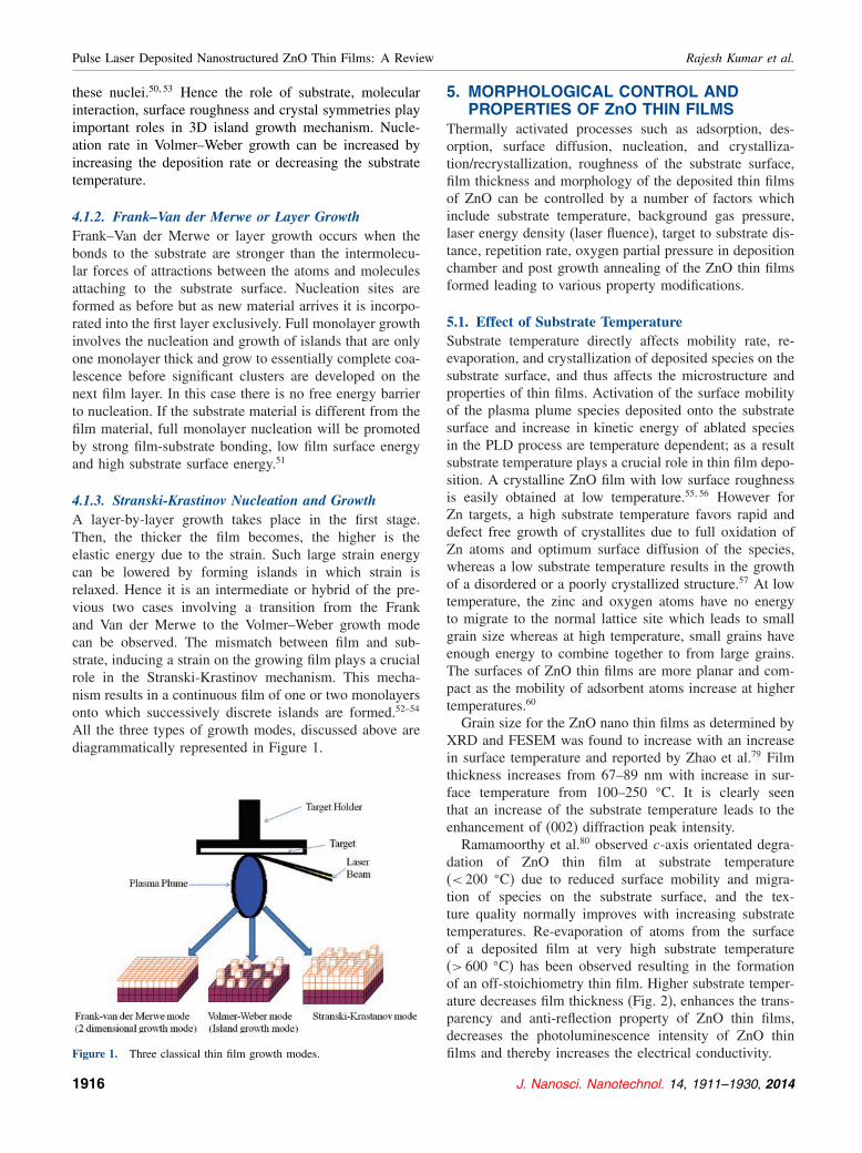
4.1. Nucleation and Growth MechanismIn PLD, condensation of the plasma plume leads to theaccumulation of plume particles by lowering of their ener-gies on the substrate surface. Lattice mismatch has amarked effect on film morphology. The strain resultingfrom lattice mismatch contributes to the interface energy,a key parameter in determining the growth mode. For het-eroepitaxial growth, depending upon the thermodynamicsthat relates the surface energies of the film and substrateand the film substrate interface energy, three types ofgrowth modes, Volmer–Weber or island growth, Frank–Van der Merwe or layer growth and Stranski–Krastanov orintermediate growth are described in literature.
4.1.1. The Volmer–Weber GrowthIt is also referred to as “3D Island Growth” which occurswhen the intermolecular forces of attractions between theatoms and molecules attaching to the substrate surface arestronger than the forces they will form with the substratematerial. In this epitaxial growth mechanism, as soon asthe nucleation sites of the first layer are formed the sec-ond layer begins to form on top. Growth of these islandscauses rough multi-layer films to grow on the substratesurface. Different orientations of island to island result asmost of the nucleation takes place on substrate surfacedefects, and islands of the deposited films grow out of
J. Nanosci. Nanotechnol. 14, 1911–1930, 2014 1915
Pulse Laser Deposited Nanostructured ZnO Thin Films: A Review Rajesh Kumar et al.
these nuclei.50�53 Hence the role of substrate, molecularinteraction, surface roughness and crystal symmetries playimportant roles in 3D island growth mechanism. Nucle-ation rate in Volmer–Weber growth can be increased byincreasing the deposition rate or decreasing the substratetemperature.
4.1.2. Frank–Van der Merwe or Layer GrowthFrank–Van der Merwe or layer growth occurs when thebonds to the substrate are stronger than the intermolecu-lar forces of attractions between the atoms and moleculesattaching to the substrate surface. Nucleation sites areformed as before but as new material arrives it is incorpo-rated into the first layer exclusively. Full monolayer growthinvolves the nucleation and growth of islands that are onlyone monolayer thick and grow to essentially complete coa-lescence before significant clusters are developed on thenext film layer. In this case there is no free energy barrierto nucleation. If the substrate material is different from thefilm material, full monolayer nucleation will be promotedby strong film-substrate bonding, low film surface energyand high substrate surface energy.51
4.1.3. Stranski-Krastinov Nucleation and GrowthA layer-by-layer growth takes place in the first stage.Then, the thicker the film becomes, the higher is theelastic energy due to the strain. Such large strain energycan be lowered by forming islands in which strain isrelaxed. Hence it is an intermediate or hybrid of the pre-vious two cases involving a transition from the Frankand Van der Merwe to the Volmer–Weber growth modecan be observed. The mismatch between film and sub-strate, inducing a strain on the growing film plays a crucialrole in the Stranski-Krastinov mechanism. This mecha-nism results in a continuous film of one or two monolayersonto which successively discrete islands are formed.52–54
All the three types of growth modes, discussed above arediagrammatically represented in Figure 1.
Figure 1. Three classical thin film growth modes.
5. MORPHOLOGICAL CONTROL ANDPROPERTIES OF ZnO THIN FILMS
Thermally activated processes such as adsorption, des-orption, surface diffusion, nucleation, and crystalliza-tion/recrystallization, roughness of the substrate surface,film thickness and morphology of the deposited thin filmsof ZnO can be controlled by a number of factors whichinclude substrate temperature, background gas pressure,laser energy density (laser fluence), target to substrate dis-tance, repetition rate, oxygen partial pressure in depositionchamber and post growth annealing of the ZnO thin filmsformed leading to various property modifications.
5.1. Effect of Substrate TemperatureSubstrate temperature directly affects mobility rate, re-evaporation, and crystallization of deposited species on thesubstrate surface, and thus affects the microstructure andproperties of thin films. Activation of the surface mobilityof the plasma plume species deposited onto the substratesurface and increase in kinetic energy of ablated speciesin the PLD process are temperature dependent; as a resultsubstrate temperature plays a crucial role in thin film depo-sition. A crystalline ZnO film with low surface roughnessis easily obtained at low temperature.55�56 However forZn targets, a high substrate temperature favors rapid anddefect free growth of crystallites due to full oxidation ofZn atoms and optimum surface diffusion of the species,whereas a low substrate temperature results in the growthof a disordered or a poorly crystallized structure.57 At lowtemperature, the zinc and oxygen atoms have no energyto migrate to the normal lattice site which leads to smallgrain size whereas at high temperature, small grains haveenough energy to combine together to from large grains.The surfaces of ZnO thin films are more planar and com-pact as the mobility of adsorbent atoms increase at highertemperatures.60
Grain size for the ZnO nano thin films as determined byXRD and FESEM was found to increase with an increasein surface temperature and reported by Zhao et al.79 Filmthickness increases from 67–89 nm with increase in sur-face temperature from 100–250 �C. It is clearly seenthat an increase of the substrate temperature leads to theenhancement of (002) diffraction peak intensity.Ramamoorthy et al.80 observed c-axis orientated degra-
dation of ZnO thin film at substrate temperature(< 200 �C) due to reduced surface mobility and migra-tion of species on the substrate surface, and the tex-ture quality normally improves with increasing substratetemperatures. Re-evaporation of atoms from the surfaceof a deposited film at very high substrate temperature(> 600 �C) has been observed resulting in the formationof an off-stoichiometry thin film. Higher substrate temper-ature decreases film thickness (Fig. 2), enhances the trans-parency and anti-reflection property of ZnO thin films,decreases the photoluminescence intensity of ZnO thinfilms and thereby increases the electrical conductivity.
1916 J. Nanosci. Nanotechnol. 14, 1911–1930, 2014

Rajesh Kumar et al. Pulse Laser Deposited Nanostructured ZnO Thin Films: A Review
Figure 2. The plot of thickness of ZnO thin films deposited at RT,200 �C and 300 �C versus substrate temperature. Reprinted with permis-sion from [80], K. Ramamoorthy, et al., Current Applied Physics 6, 103(2006). © 2006, Elsevier.
Optical transmittance (T ) in the visible range(400–700 nm) is also found to increases slightly withincreasing the substrate temperature from room tempera-ture to 300 �C, and is related to the increase in grain size ofthe films with increasing substrate temperature.58�79�81�150
Increased optical transmission of the ZnO thin films is dueto high mobility of the charge carriers, reduction of freecarrier absorption, ability of the film surface roughnessto reduce reflectivity, increase of a structural homogene-ity, fine texturing and decrease of the diffuse scattering.80
Columnar structured c-axis oriented ZnO thin films grownon Si (111) and Si (100) substrates at growth temperaturesfrom 500 to 675 �C and oxygen pressures from 3× 10⁻²
to 10 Pa, as confirmed by XRD, AFM, and TEM investi-gations, show diametric growth on the increasing growthtemperature without any explicit dependence of the grainsize on the oxygen pressure.82–84
Zeng et al.59�85 in temperature range of 200–600 �Cstudied deposition of ZnO films on (0001) sapphire�-Al2O3 substrate and found decrease in deposition rateabove 400 �C but better crystalline qualities as com-pared to low temperature. At higher temperatures Znand O2 molecules have too much thermal energy andO2 molecules begin to resputter. Similar results wereobtained by Liu et al.61�86 for the deposition of ZnO onglass and silicon substrates between substrate tempera-ture 200–500 �C. However, good crystalline nature ofZnO thin films grown on Si (111) substrate at a tem-perature of 600 �C is observed by Jianting.62 A closecorrelation is observed between surface roughness andsubstrate temperature. The surface roughness, related tograin size generally increases as the substrate temperatureincreases.63–65�96�115�123�125�129�132–134�140
The intensity of UV PL peaks increases markedly withthe increases of substrate temperature. Strong UV lumi-nescence obtained by increasing the substrate tempera-tures of ZnO films make them possible for using inlight emission device applications. Ultraviolet (UV) sensi-tive films deposited by Ayouchi et al.69 exhibit maximum
sensitivity at lower temperature than the films depositedat higher temperatures which show crystallite sizes of typ-ically 500 nm, a high dark current and minimum photoresponse. More densely packed crystallites and a fasterdecay in photocurrent is observed for films deposited atlower temperature.To conclude, the ZnO thin films exhibit low sur-
face roughness, more thickness, small grain size, lowoptical transmittance, maximum sensitivity, high surfaceconductivity, good conductive uniformity, increased bandgap, more oxygen vacancies, low mobility of the chargecarriers, low reflectivity, decreased structural homogene-ity and increased diffuse scattering with lower substratetemperature.
5.2. Effect of Oxygen Partial PressureAfter initial free expansion from the target surface, themean free path of the ablated particles is reduced in thepresence of gas. At higher ambient pressure, the more col-lisions and scatterings occur; particles lose energy to formionic complexes or molecules. These clusters reach thesubstrate surface and small grain particles start to growas they become the nucleus. On the other hand, most ofthe ablated particles can reach the substrate in the statenear the single atoms if the ambient pressure is extremelylow.41 Hence, Oxygen pressure in the deposition chamberof PLD apparatus influences both the deposition rate andthe kinetic energy of ejected ablated species. The thick-ness of the ZnO films also increases with increasing theoxygen partial pressure.87
With the increase of O2 partial pressure, the kineticenergy of the ablated species reduces due to a large num-ber of collisions with background gas molecules and thesize of ablated plume decreases.53 The higher the O2 pres-sure in the growth chamber, the more oxygen is incorpo-rated into the ZnO film lattice. When oxygen is excessivelyincorporated due to a high O2 pressure, lattice expansionsare likely to happen. At lower oxygen pressure, the ablatedspecies have sufficient kinetic energy for diffusion and canthus diffuse to the right crystallographic sites. However,at higher oxygen pressure, the ablated species have lesskinetic energy which results in less diffusion resulting inpoor crystalline quality of the films. Films deposited undervery low pressure are often oxygen deficient, and therebyaffect the micro structural and electrical properties.66�88
Oxygen pressure also influences the mean free path of theablated species, which increases with decreasing O2 partialpressure. The processing of film at very low oxygen pres-sures is generally known as laser molecular-beam epitaxy(LMBE) where the mean free path of the plume speciesis much larger than the target to substrate distance.67
Chupoon et al.68 deposited ZnO thin films at low oxygenpressure of 10−5 to 10−4 Torr to form compressive strainedc-axis lattice parameter larger than the bulk value. How-ever, this strain was reduced for higher oxygen pressures
J. Nanosci. Nanotechnol. 14, 1911–1930, 2014 1917

Pulse Laser Deposited Nanostructured ZnO Thin Films: A Review Rajesh Kumar et al.
(10−2 Torr) deposition with minimal surface roughness.The ZnO thin films exhibit low surface roughness, highsurface conductivity, and good conductive uniformity withlower oxygen pressure.Zhaoyang et al.70 studied the oxidation rates of ZnO
thin films grown on sapphire (001) substrate between 1 to500 mTorr O2 pressures at 400
�C. ZnO grain growth rateretards and fine ZnO grain structure forms at low oxygenpartial pressures. As the oxygen partial pressure increases,the oxidation rate increases, leading to large ZnO grains.Moreover, as the oxygen partial pressure increases, the for-mation of ZnO gas is enhanced by the collisions betweenthe Zn and oxygen in this nonthermal equilibrium case ofPLD.Very high pressure oxygen treatment of 5 atm on
ZnO thin films deposited on Sapphire (0001) substrate at500 �C by the pulsed laser deposition for 24, 72, 240and 480 h, respectively enhanced the intensities of defectpeaks at 2.1 and 2.5 eV without affecting near band edge(NBE). A decreased carrier concentration and increasedmobility has been observed by the high pressure oxygentreatment.71�104
Optical transmission of the ZnO films at high oxygenpressure is lower than for low oxygen pressure, and isdue to the grain size. The lower the oxygen pressure,the smaller the grain size.41�78 The oxygen pressure alsoaffects the direct band gap of the ZnO thin films. Thedecrease in the direct band gap with an increase in oxy-gen pressure is due to a decrease in carrier concentrationas explained by the Burstien—Moss effect.53�89 At higheroxygen pressure transparency of the deposited ZnO thinfilms is enhanced as shown in Figure 3. The superior opti-cal transmission of the ZnO thin films could be dominantlydue to the ability of the film surface roughness to reduce
Figure 3. Transmission spectra for the ZnO films deposited with var-ious oxygen pressures. Reprinted with permission from [89], C. F. Yu,et al., Appl. Surf. Sci. 256, 792 (2009). © 2009, Elsevier.
reflectivity, an increase in the structural homogeneity, finetexturing and the approach of the film composition to thestoichiometry.89�90�117�126–128�146
Two emission bands in PL UV were apparentlyobserved for all the thin films: one is the near-band-edgeemission (NBE) peak at the UV region, which is dueto the carrier’s recombination from band to band, andthe other was the deep-level-emission (DLE) peak aroundthe green–yellow band that corresponds to the transitionof the excited optical center from the deep level to thevalence band. With the increase in oxygen pressure, theintensity of the DLE peak decreases remarkably and thatof the NBE peak increases rapidly as shown in Figure 4.The intensity of DLE peak is generally proportional tothe conductivity. The strong DLE peak is found to bestrongly dependent on the oxygen pressure. This is prob-ably because the stoichiometry of oxygen-deficient ZnOfilm with less oxygen vacancies and radiative transitionsbetween shallow donors (O vacancy and Zn interstitial)and deep acceptor (Zn vacancy), is improved by increas-ing oxygen pressure.89�91 The PL intensity of ultra-violet(UV) luminescence and the dependent electrical resistiv-ity generally increase as the oxygen pressure for the PLDof ZnO increases. At the lower oxygen pressure withthe largest number of oxygen vacancies, correspondinglythe electron concentration and the conductivity is thushigher than other samples grown at the higher oxygenpressure.132�137�139
Figure 4. The PL spectra of the ZnO films grown under the conditionsof oxygen pressure of 50, 300, 400 and 500 mTorr at the substrate tem-perature of 400 �C. Reprinted with permission from [91], B. J. Jin, et al.,Appl. Surf. Sci. 169–170, 521 (2001). © 2001, Elsevier.
1918 J. Nanosci. Nanotechnol. 14, 1911–1930, 2014
Rajesh Kumar et al. Pulse Laser Deposited Nanostructured ZnO Thin Films: A Review
To conclude the ZnO thin films exhibit low surfaceroughness, more thickness, high surface conductivity,lower electrical resistivity, good conductive uniformity,increased band gap, more oxygen vacancies, high electronconcentration and increased DLE peak intensity at loweroxygen pressure.
5.3. Effect of Post AnnealingAfter the thin films are prepared under certain ambi-ent conditions, crystallinity, stoichiometric ratio, surfacemorphology and hence, the transmittance and electri-cal properties of the thin films can be further modifiedby annealing treatment. From literature most ZnO filmswere deposited on crystal substrates at substrate tem-perature from room temperature (RT) to about 400 �Ctemperature.92 Substrate materials, such as glass and poly-mer cannot be subjected to a higher temperature anneal-ing, thus low temperature annealing; also referred to asaging of thin films under RT and air atmosphere fora long time may be an alternate approach to furtherimprove the properties of thin films. Post annealing tem-perature is usually higher 200–800 �C,93 800 �C,94�95
400–800 �C,96–98�132 400–700 �C,99 300–800 �C.100�101
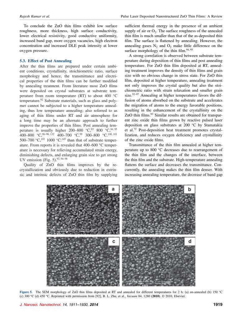
500–700 �C,102 1000 �C:145 than that of substrate temper-ature. From reports it is revealed that 400–600 �C temper-ature is necessary for relieving accumulated strain energy,diminishing defects, and enlarging grain size to get strongUV emission (Fig. 5).92�94–98
Quality of ZnO thin films improves by the re-crystallization and obviously due to reduction in extrin-sic and intrinsic defects of ZnO thin film by supplying
Figure 5. The SEM morphology of ZnO thin films deposited at RT and annealed for different temperatures for 2 h: (a) un-annealed (b) 150 �C(c) 300 �C (d) 450 �C. Reprinted with permission from [92], B. L. Zhu, et al., Vacuum 84, 1280 (2010). © 2010, Elsevier.
sufficient thermal energy in the presence of an ambientsupply of air or O2. The surface roughness of the annealedthin film is much smaller than that of the as-deposited thinfilm. The surface is flattened by annealing. However, theannealing gases N2 and O2 make little difference on thesurface morphology of the thin film.94�95
A strong correlation is observed between substrate tem-perature during deposition of thin films and post annealingtemperature. For ZnO thin film deposited at RT, anneal-ing treatment improves the density of thin films and grainsize with no obvious change in stress state. For ZnO thinfilm, deposited at higher temperature, annealing treatmentnot only improves the crystal quality but also the stoi-chiometric ratio with strain relaxation and smaller grainsize.92–97 Annealing at higher temperatures favors the dif-fusion of atoms absorbed on the substrate and acceleratesthe migration of atoms to the energy favorable positions,resulting in the enhancement of the crystallinity on theZnO thin films.93 Similar results are obtained for transpar-ent zinc oxide thin films grown by reactive pulsed laserdeposition on glass substrates at 200 �C by Stamatakiaet al.72 Post-deposition heat treatment promotes crystal-lization, and reduces oxygen deficiency and crystallinityof the zinc oxide films.Transmittance of the thin film annealed at higher tem-
perature up to 800 �C decreases due to rearrangement ofthe thin film and the changes of the interface, betweenthe thin film and the substrate. High-temperature annealingflattens the surface and decreases the transmittance. Con-currently, the annealing makes the thin film denser. Withincreasing annealing temperature, the decrease of band gap
J. Nanosci. Nanotechnol. 14, 1911–1930, 2014 1919
Pulse Laser Deposited Nanostructured ZnO Thin Films: A Review Rajesh Kumar et al.
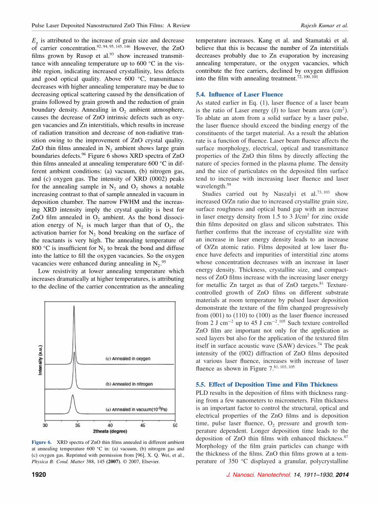
Eg is attributed to the increase of grain size and decreaseof carrier concentration.92�94�95�145�146 However, the ZnOfilms grown by Rusop et al.93 show increased transmit-tance with annealing temperature up to 600 �C in the vis-ible region, indicating increased crystallinity, less defectsand good optical quality. Above 600 �C, transmittancedecreases with higher annealing temperature may be due todecreasing optical scattering caused by the densification ofgrains followed by grain growth and the reduction of grainboundary density. Annealing in O2 ambient atmosphere,causes the decrease of ZnO intrinsic defects such as oxy-gen vacancies and Zn interstitials, which results in increaseof radiation transition and decrease of non-radiative tran-sition owing to the improvement of ZnO crystal quality.ZnO thin films annealed in N2 ambient shows large grainboundaries defects.96 Figure 6 shows XRD spectra of ZnOthin films annealed at annealing temperature 600 �C in dif-ferent ambient conditions: (a) vacuum, (b) nitrogen gas,and (c) oxygen gas. The intensity of XRD (0002) peaksfor the annealing sample in N2 and O2 shows a notableincreasing contrast to that of sample annealed in vacuum indeposition chamber. The narrow FWHM and the increas-ing XRD intensity imply the crystal quality is best forZnO film annealed in O2 ambient. As the bond dissoci-ation energy of N2 is much larger than that of O2, theactivation barrier for N2 bond breaking on the surface ofthe reactants is very high. The annealing temperature of800 �C is insufficient for N2 to break the bond and diffuseinto the lattice to fill the oxygen vacancies. So the oxygenvacancies were enhanced during annealing in N2.
95
Low resistivity at lower annealing temperature whichincreases dramatically at higher temperatures, is attributingto the decline of the carrier concentration as the annealing
Figure 6. XRD spectra of ZnO thin films annealed in different ambientat annealing temperature 600 �C in: (a) vacuum, (b) nitrogen gas and(c) oxygen gas. Reprinted with permission from [96], X. Q. Wei, et al.,Physica B: Cond. Matter 388, 145 (2007). © 2007, Elsevier.
temperature increases. Kang et al. and Stamataki et al.believe that this is because the number of Zn interstitialsdecreases probably due to Zn evaporation by increasingannealing temperature, or the oxygen vacancies, whichcontribute the free carriers, declined by oxygen diffusioninto the film with annealing treatment.72�100�101
5.4. Influence of Laser FluenceAs stated earlier in Eq. (1), laser fluence of a laser beamis the ratio of Laser energy (J) to laser beam area (cm2).To ablate an atom from a solid surface by a laser pulse,the laser fluence should exceed the binding energy of theconstituents of the target material. As a result the ablationrate is a function of fluence. Laser beam fluence affects thesurface morphology, electrical, optical and transmittanceproperties of the ZnO thin films by directly affecting thenature of species formed in the plasma plume. The densityand the size of particulates on the deposited film surfacetend to increase with increasing laser fluence and laserwavelength.59
Studies carried out by Naszalyi et al.73�103 showincreased O/Zn ratio due to increased crystallite grain size,surface roughness and optical band gap with an increasein laser energy density from 1.5 to 3 J/cm2 for zinc oxidethin films deposited on glass and silicon substrates. Thisfurther confirms that the increase of crystallite size withan increase in laser energy density leads to an increaseof O/Zn atomic ratio. Films deposited at low laser flu-ence have defects and impurities of interstitial zinc atomswhose concentration decreases with an increase in laserenergy density. Thickness, crystallite size, and compact-ness of ZnO films increase with the increasing laser energyfor metallic Zn target as that of ZnO targets.81 Texture-controlled growth of ZnO films on different substratematerials at room temperature by pulsed laser depositiondemonstrate the texture of the film changed progressivelyfrom (001) to (110) to (100) as the laser fluence increasedfrom 2 J cm−2 up to 45 J cm−2.105 Such texture controlledZnO film are important not only for the application asseed layers but also for the application of the textured filmitself in surface acoustic wave (SAW) devices.74 The peakintensity of the (002) diffraction of ZnO films depositedat various laser fluence, increases with increase of laserfluence as shown in Figure 7.81�103�105
5.5. Effect of Deposition Time and Film ThicknessPLD results in the deposition of films with thickness rang-ing from a few nanometers to micrometers. Film thicknessis an important factor to control the structural, optical andelectrical properties of the ZnO films and is depositiontime, pulse laser fluence, O2 pressure and growth tem-perature dependent. Longer deposition time leads to thedeposition of ZnO thin films with enhanced thickness.87
Morphology of the film grain particles can change withthe thickness of the films. ZnO thin films grown at a tem-perature of 350 �C displayed a granular, polycrystalline
1920 J. Nanosci. Nanotechnol. 14, 1911–1930, 2014

Rajesh Kumar et al. Pulse Laser Deposited Nanostructured ZnO Thin Films: A Review
Figure 7. XRD spectra of ZnO films deposited on glass substrates atvarious laser energies. Reprinted with permission from [81], B. L. Zhu,et al., Physica B 396, 95 (2007). © 2007, Elsevier.
morphology, which transforms to nano or micro rod as thethickness of the film increases.106�107 Films deposited fora small 5-minute duration show no characteristic wurtzitestructures for ZnO due to the strain originating from thelattice mismatch between the film and the substrate. Theratio of oxygen to zinc (O/Zn) is larger than unity andbecomes closer to unity for the films with longer deposi-tion times thereby improving crystallinity.108
The effect of the thickness variation on the surfacemorphology and structural, electrical, and optical prop-erties of ZnO thin films grown on c-plane sapphire byPLD reveals that, as the film thickness increases, the crys-tallinity and optical and electrical properties of ZnO thinfilms improves. Furthermore, ZnO films with thickness400 nm or more exhibit the near-bulk properties. ZnO thinfilms with a thickness of 40 nm show a smooth surfacewith several islands indicating the film layer-plus-islandgrowth mode (Stranski-Krastinov mode) and for the filmswith a thickness of 170 and 400 nm, a rough surfaceis observed with 3D-island growth mode (Volmer–Webergrowth) as discussed in Section 4.3.1. The tensile strain inthe films decreases with increasing film thickness result-ing in better crystalline quality as indicated by a moreintense peak for (002) diffraction of ZnO films depositedwith various film thicknesses.109 The increase in ZnO filmthickness also results in the improvement of the opticalproperties, and may be due to the decrease of strain at theinterface between ZnO film and sapphire substrate by theincrease of film thickness.Park et al. found that the films thinner than 400 nm
are under a severe misfit strain, which decreases as thefilm thickness increases further.75 Electrical resistivitydecreases significantly with increasing thickness due tothe highest carrier concentration and fewer point defectslike oxygen vacancies. The conductivity of ZnO thin filmscan probably be attributed to oxygen vacancies and Zn
interstitials which are donor type point defects. Hence theenhancement of the defects leads to the rise of carrierconcentration.5 On the contrary, the decrease of defectswith increase of the thickness of ZnO thin films causes thedecline of carrier concentration, or the increase of resistiv-ity. For very thick films auto-doped carrier concentrationbecomes constant.109
5.6. Effect of Pulse Repetition RateThe amount of ablated species arriving on a substrate perlaser shot increases as pulse repetition rate is increased.King et al.110 studied the effect of laser repetition rates of10, 5 and 2 Hz for ZnO thin films grown on Si substratesat 300 �C. The film crystallinity was found to be sensi-tive to the pulse repetition rate with constant number ofpulses and yielded film thicknesses of 272 nm, 289 nmand 255 nm respectively, as characterized by ellipsometry.The grain size of ZnO thin film deposited at 5 Hz waslarger than that of 10 Hz. The variation of repetition ratesdoes not have an effect on the optical property of ZnOthin films as UV emission intensity/visible emission inten-sity ratios of ZnO thin films deposited at 5 Hz and 10 Hzare almost identical. Lee have reported the degradationof the crystalline quality and surface morphology in ZnOthin film deposited at 10 Hz results from super saturationeffect by decrease of time interval between a ZnO particlearriving on a substrate by laser shot and a ZnO particlearriving on a substrate by next laser shot.111 During thestudy of effect of pulse repetition rate other experimentalparameters, such as substrate temperature, energy densityof the laser, ambient gas pressure and the distance betweena target and substrate are kept constant.
5.7. Effect of Target to Substrate DistanceThe oxygen partial pressure in the chamber, the target-to-substrate distance and the laser energy density has synergiceffect in determining the energy of the ablated particleswhen they reach the substrate. As the plume particles canthermalize completely at high O2 pressure, their kineticenergy reduces due to large number of collisions withbackground gas molecules and hence a decrease in the sizeof ablated plume is observed.12 However, at high vacuumor low O2 pressure the mean free path of the energizedions and particulates is longer; so, the particles bombardthe substrate to form a crystalline or polycrystalline film.Therefore it is better to reduce the distance between thetarget and substrate while working at higher pressures tomaintain the optimum energy of the ablated species.30 Atlow pressure working conditions, however, samples grownat shorter target–substrate distance may develop defects,cracks or peeling off. On the other hand the films grownat longer distance are homogenous, smooth, adherent, andwithout cracks.112
In the deposition chamber with the smaller target to thesubstrate distance, a strong dependence of carrier concen-tration on oxygen partial pressure is observed.77 The Hall
J. Nanosci. Nanotechnol. 14, 1911–1930, 2014 1921

Pulse Laser Deposited Nanostructured ZnO Thin Films: A Review Rajesh Kumar et al.
TableI.
Physical
parametersforun-doped
ZnO
thin
filmsdepositedby
PLD
techniqueandcrystallo
graphicorientation.
Laser
Laser
source,
Pulse
energy
/Oxy
gen
Film
Backg
roun
dPo
stwavelength(nm),
rate
fluence
partial
thickn
ess
cham
ber
Td
annealing
Cryslallographic
References
Precursor
Substrate
pulsedu
ratio
n(H
z)(J/cm
2)
Ts(�C)
pressure
(nm)
pressure
(cm)
Temp.
(�C)
data
S.Cho
[58]
ZnO
c-Sapph
ire
KrF
248
52
400–
700
––
–6
–(0
02)
S.J.Kanget
al.[63]
ZnO
Si(100
)KrF
248
52
100–
700
250mTo
rr–
5×1
0−6To
rr–
––
C.S.
Sonet
al.[64]
ZnO
Si(100
)KrF
248
52
400
350mTo
rr–
–6
–(002
),(004
)50
0(002
),(103
)60
0(101
),(103
)Y.R.Ryu
etal.[65]
ZnO
GaA
sArF
193
202
300–
450
20–5
0mTo
rr0.7–
1.1a
8×1
0−7
7–
(0002)
R.Ayo
uchi
etal.[69]
ZnO
c-Sapph
ire
Nd:YAG
355
––
400,
500
0.25
mbar
––
5–
(002)
5ns
W.Zhaoyanget
al.[70]
ZnO
Si(111
)KrF
248
52.5
650
0–80
Pa–
10−8
Pa5
–(0
02)
25ns
B.I.Kim
etal.[71]
ZnO
Sapp
hire
(000
1)KrF
248
52.1
500
5atm
450–
603
10−8
Pa–
–(000
2),(000
4)K.Sh
rinivasrao
etal.[78]
ZnO
Quartzglass,
KrF
248
515
6∗20
0–60
00.05
–0.5
mbar
456
10−7
mBar
––
(002)
Si(100
)25
nsL.Zhaoet
al.[79]
ZnMetal
Quartzglass
Nd:YAG
1064
107
100–
250
11Pa
67–8
95×1
0−4Pa
2.3
–(002
),(103
)weak
100ns
K.Ram
amoorthy
etal.[80]
ZnO
Glass
Nd:YAG
355
105
RT,
200,
10−5
Torr
0.66
,8,
13a
10−6
Torr
6–
–6ns
300
B.L.Zhu
etal.[81]
ZnMetal
Glass
KrF
248
510
0–RT
100Pa
60–4
003×1
0−3Pa
5–
Amorph
ous
25ns
325∗
200
(002
)50
0(002
)S.
Heitsch
etal.[82]
ZnO
Silic
on(100
),KrF
248
1–
500–
675
3×1
0−2–1
0Pa
300–
700
–5.5
–(000
2),(000
4)(111
)25
nsKaidashev
etal.[84]
ZnO
c-Plane
sapp
hire
KrF
248
1–
600–
750
2.5×1
0−2,
1–2a
–5.5
––
25ns
5×1
0−4mbar
S.H.Bae
etal.[85]
ZnO
Sapp
hire
(000
1)Nd:YAG
355
52.5
200–
600
10−6–4
00mTo
rr1a
1×1
0−6To
rr5
–(0
02)
V.Craciun
etal.[86]
ZnO
Silic
on(100
),KrF
248
–0.5–
520
0–50
05×1
0−6–
632
10−6–1
0−7To
rr4
–(002
),(004
)Corning
glass
2×1
0−2To
rrS.
Fiat
etal.[87]
ZnMetal
Soda
limeglass
KrF
248
102.6
300
10,15
Pa27
5–30
610
−4Pa.
5–
(002
),(004
)10
nsLiu
etal.[88]
ZnO
Sapp
hire,Silic
onKrF
248
–25
0∗55
0–70
00.25
–20To
rr–
5–20
Torr
2–4.2
–(002
)(004
)(006
)25
nsC.F.
Yuet
al.[89]
ZnO
Glass
Nd:YAG
532
–18
.5∗
150
40–1
50mTo
rr–
10−6
Torr
2.5
–(0
02)
7ns
J.B.Franklin
etal.[90]
ZnO
ITO
KrF
248
80.85
50–6
505or
50mTo
rr12
0–25
03×1
0−5To
rr5
–(0
02)
25ns
B.J.Jinet
al.[91]
ZnO
Sapp
hire
(001
)Nd:YAG
355
52.5
400
50mTo
rr0.6–
1.8a
5×1
0−5To
rr5
400
Un-annealed
(002
),20
0mTo
rr(101
),(100
)30
0mTo
rrAnn
ealedat
400mTo
rr40
0mTo
rr(002
)50
0mTo
rrB.L.Zhu
etal.[92]
ZnO
Glass
KrF
248
52.78
200–
500
12Pa
150–
200
3×1
0−3Pa
715
0–45
0(0
02)
25ns
1922 J. Nanosci. Nanotechnol. 14, 1911–1930, 2014

Rajesh Kumar et al. Pulse Laser Deposited Nanostructured ZnO Thin Films: A Review
TableI.
Con
tinued.
Laser
Laser
source,
Pulse
energy
/Oxy
gen
Film
Backg
roun
dPo
stwavelength(nm),
rate
fluence
partial
thickn
ess
cham
ber
Td
annealing
Cryslallographic
References
Precursor
Substrate
pulsedu
ratio
n(H
z)(J/cm
2)
Ts(�C)
pressure
(nm)
pressure
(cm)
Temp.
(�C)
data
M.Rusop
etal.[93]
ZnO
Si(100
)XeC
l30
810
5.2
RT
6To
rr–
2×1
0−5To
rr45
RT
(100
)(00
2)(101
)20
0(100
)(002
)(101
)30
0–80
0(002
)F.
K.Sh
anet
al.[94]
ZnO
Sapp
hire
(000
1)KrF
248
52
400
200mTo
rr–
–50
800
–10
nsN
2,O
2Atm
.F.
K.Sh
anet
al.[95]
ZnO
Sapp
hire
(000
1)KrF
248
51
100–
300
200mTo
rr–
–50
800
(002)
25ns
400–
600
(002
),(004
)X.Q.Wei
etal.[96]
ZnO
Si(111
)Nd:YAG
1064
1020
0∗40
00.13
pa60
05.6×1
0−5Pa
440
0–80
0(0
02)
10ns
F.K.Sh
anet
al.[98]
ZnO
Si(100
)KrF
248
51
100–
600
200mTo
rr–
–5
400–
600
–25
nsS.
H.Bae
etal.[99]
ZnO
Si(100
)Nd:YAG
355
52.5
400
350mTo
rr–
1×1
0−6To
rr5
400–
700
(002)
Kanget
al.[100
]ZnO
Sapp
hire
(001
)Nd:YAG
355
52.5
400
350mTo
rr70
0–80
0–
540
0(002
)80
0(100
)(002
)(101
)L.Zhaoet
al.[102
]ZnMetal
Quartzglass
Nd:YAG
1064
107,
7.6
100–
250
50pa
–5×1
0−4Pa
–50
0−70
0(0
02)
100ns
Venkatachalam
etal.[103
]ZnO
Glass
andsilic
onKrF
248
101.5–
330
0.02
5mbar
244
4×1
0−5mbar
3.5
–(100
)(002
)(101
)B.L.Zhu
etal.[104
]ZnO
Amorph
ousglass
KrF
248
534
8∗–
0.2,
24,15
0Pa
140
3×1
0−3Pa
5–
(002)
25ns
J.I.Hon
get
al.[105
]ZnO
Silic
onwafers,
KrF
248
305–
4585
0–
700
10−6
Torr
4–
(100
)(002
)(101
)Kaptonfilms,
Glass
plates
S.Christoulakis
etal.[106
],[107
]ZnO
Corning
1737
FXeC
l30
8–
–35
056
0To
rr10
nm−1
a–
––
(002
),(004
)glass
Y.R.Jang
etal.[108
]ZnO
Si(100
)Not
specified
––
600
–10
0–40
0–
–(0
02)
J.M.Myo
unget
al.[109
]ZnO
Sapp
hire
(000
1)Nd:YAG
355
52.5
400
350mTo
rr40
–240
01×1
0−6To
rr5
–(0
02)
Kinget
al.[110
]ZnO
Com
ing70
59KrF
248
2,5,
520
0–50
0I.3
mTo
rr28
9–25
5–
––
(002)
glass,
25ns
10pu
requ
artz,
Si(100
)J.W.Kim
etal.[111
]ZnO
Sapp
hire
(001
)Nd:YAG
355
5,10
2.5
400
350mTo
rr10
0010
−6–1
0−7To
rr5
––
J.Dattatray
etal.[113
]ZnO
W,Refoil
Nd:YAG
355
101
600
10−4
mBar
–10
−6mBar
5–
(002)
6ns
A.O.Dikovskaet
al.[114
]ZnO
SiO
2(001
)XeC
l30
82
–25
–500
0.05
–0.3
mbar
450–
650
10−5
mbar
4–
(002)
30ns
Hvonet
al.[115
]ZnO
ZnO
wafers
KrF
248
5–
470–
700
0.01
6mbar
1a–
––
J.Zhang
etal.[116
]ZnO
�-G
a 2O
3(100
)KrF
248
–5
600
150mTo
rr20
0–
4–
(002)
25ns
K.J.Sa
jiet
al.[117
]ZnO
Quartz,
Silic
on,
Nd:YAG
355
103
RT
0.00
7–0.00
3mbar
200
10−6
mbar
4–
(002)
andPo
lymer,
9ns
Al 2O
3(000
1)
J. Nanosci. Nanotechnol. 14, 1911–1930, 2014 1923

Pulse Laser Deposited Nanostructured ZnO Thin Films: A Review Rajesh Kumar et al.
TableI.
Con
tinued.
Laser
Laser
source,
Pulse
energy
/Oxy
gen
Film
Backg
roun
dPo
stwavelength(nm),
rate
fluence
partial
thickn
ess
cham
ber
Td
annealing
Cryslallographic
References
Precursor
Substrate
pulsedu
ratio
n(H
z)(J/cm
2)
Ts(�C)
pressure
(nm)
pressure
(cm)
Temp.
(�C)
data
L.C.Nistoret
al.[118
]Zn
MgO
(001
)Nd:YAG
355
1020
500
–18
010
−3Pa
5.5
–(110
0),(110
1),
(112
0),
(000
2)weak
L.Z.Fu
etal.[119
]ZnO
c-Sapph
ire
KrF
248
51
100–
500
200mTo
rr–
–5
–(000
2),(000
4)M.Novotny
etal.[120
]Sa
pphire
(000
1),
Nd:YAG
266
102.8
300
10Pa
802×1
0−4Pa.
5.5
–(002
),(103
)MgO
(100
),6ns
fusedsilic
aRahman
etal.[121
]ZnMetal
Calcite
(CaC
O3)
Nd:YAG
1064
–10
∗RT
10−3
torr
–10
−3torr
5–
(100
),(101
),(102
)9–
14ns
M.Khalid
etal.[122
]ZnO
a-plane
Al 2O
3KrF
248
–2
300–
400
––
––
–ZnO
(000
2)/A
l 2O
3
c-plane
Al 2O
3(112
0)ZnO
(000
2)/A
l 2O
3
r-planeAl 2O
3(000
1)ZnO
(112
0)/
Al 2O
3(011
2)M.Z.Lin
etal.[123
]ZnO
Al 2O
3(000
1)Nd:YAG
355
102
600–
900
10−5–3
×10−
4To
rr3×1
0−8To
rr5
–ZnO
[101
0]/
15ns
sapp
hire[112
0]G.Cramer
etal.[124
]ZnO
Pt/SiO
2/Si
KrF
248
635
0∗35
0–
240
10−6
Torr
––
–20
nsP.
Pant
etal.[125
]ZnO
r-Planesapp
hire
KrF
248
52–
320
0–70
02×1
0−4torr
300
7×1
0−7torr
––
–25
nsS.
S.Kim
etal.[126
]ZnO
Si(001
)KrF
248
53
600
5×1
0−4To
rr25
0–35
510
−6To
rr4
–(002
),(004
)30
ns5×1
0−3To
rr(002
),(004
)5×1
0−2To
rr(002
),(004
)5×1
0−1To
rr(002
),(101
),(102
)Amirhagh
iet
al.[127
]ZnO
Corning
glass
Nd:YAG
532
52.5–
330
02×1
0−6–2
×10−
2torr
300–
1000
10−7
torr
––
(002)
7059
,Si(100
)4ns
S.Karam
atet
al.[128
]ZnO
sapp
hire
(001
)Nd:YAG
532
1047
400
0.1–
1mbar
607×1
0−5mbar
5–
(002
),(004
)8ns
T.Ohshimaet
al.[129
]ZnO
Si(100
),KrF
248
102
RT-70
06.67
×10−
3–
242–
1520
––
–(002
),(004
)silic
aglass,
25ns
26.7
Pa�-A
l 2O
3(000
1),
corning70
59glass
V.Craciun
etal.[130
]ZnO
GaA
sKrF
248
–2.1
250
1.33
×10−
3To
rr–
–4
–(002
),(004
)20
nsW.S.
Huet
al.[131
]ZnO
,Fu
sedSilic
a,KrF24
82–
5–
375
27pa
––
––
(002)
Al 2O
3Al 2O
3(001
)X.Q
wie
etal.[132
]ZnO
c-sapph
ire
Nd:YAG
1064
1020
0∗40
0–80
0Various
800
5×1
0−6pa
4–
(002)
10ns
X.Su
net
al.[133
]ZnO
c-sapph
ire
ArF
193
106
500–
800
10mTo
rr65
0–42
010
−7To
rr5
–(000
1)ZnO
/(00
01)
(101
0)ZnO
/(11
20)
X.M.Fanet
al.[134
]ZnMetal
Si(111
)Nd:YAG
1064
1031
300–
550
11Pa
0.8–
1.3a
5×1
0−4Pa
2.5
–(100
)(002
)(101
)10
0ns
1924 J. Nanosci. Nanotechnol. 14, 1911–1930, 2014

Rajesh Kumar et al. Pulse Laser Deposited Nanostructured ZnO Thin Films: A Review
TableI.
Con
tinued.
Laser
Laser
source,
Pulse
energy
/Oxy
gen
Film
Backg
roun
dPo
stwavelength(nm),
rate
fluence
partial
thickn
ess
cham
ber
Td
annealing
Cryslallographic
References
Precursor
Substrate
pulsedu
ratio
n(H
z)(J/cm
2)
Ts(�C)
pressure
(nm)
pressure
(cm)
Temp.
(�C)
data
Y.Zhang
etal.[135
]ZnO
Si(111
)KrF
248
532
0∗35
01mTo
rr97
––
–(002
),(004
)45
021
2(002
)Y.Inou
eet
al.[136
]ZnO
R-face(011
2)ArF
193
101
––
150
10−5
Pa3.5
––
sapp
hire
Y.R.Ryu
etal.[137
]Zn
GaA
s(001
)ArF
193
201.3–
1.9
350
35,50
mTo
rr10
08×1
0−7To
rr7.5
–(0
02)
Z.Q.Chenet
al.[138
]ZnO
ZnO
(000
1),
KrF
248nm
10–
500
10−2
Torr
1–2a
––
–(000
2),(000
4)Al 2O
3(112
0)25
nsS.
Imet
al.[139
]ZnO
Sapp
hire
(001
)Nd:YAG
1064
52.5
400
1–20
0mTo
rr0.6–
1.8a
5×1
0−5To
rr5
–(0
02)
500mTo
rr(002
),(004
)F.
K.Sh
anet
al.[140
]ZnO
Glass
KrF
248
51
RT
100mTo
rr–
–5
400–
500
Amorph
ous
25ns
500
(002)
E.S.
Shim
etal.[141
]ZnO
Indium
phosph
ide
Nd:YAG
355
22.5
400
350mTo
rr32
01×1
0−6To
rr5
400–
600
(0002)
J.Duclere
etal.[142
]ZnO
Ptfilm
onNd:YAG
266
21.4
450
–50
0–
––
ZnO
(000
1)/Pt(111
)c-sapph
ire
J.H.Jo
etal.[146
]ZnO
Sapp
hire
(001
)KrF24
85
–50
05–
150mTo
rr–
2×1
0−6To
rr4
900
(002)
20ns
Y.W.Su
net
al.[147
]ZnO
SiKrF24
8–
3–
100mTo
rr–
–5
600
(100
)(002
)(101
)25
ns
Notes:(∗)Laser
energy
inmJ/pulse,
(a)Film
thichnessin
�m
units,(T
s)Su
bstrateTemperature,(T
d)Target-Substrate
distance.
J. Nanosci. Nanotechnol. 14, 1911–1930, 2014 1925

Pulse Laser Deposited Nanostructured ZnO Thin Films: A Review Rajesh Kumar et al.
mobility at room temperature of ZnO films on c-planesapphire grown by a multistep PLD process with low-temperature nucleation layers depicts highest mobility val-ues in a narrow carrier concentration range. A much weakerdependence of carrier concentration and Hall mobility onthe oxygen partial pressure was found for PLD growthof ZnO thin films at larger 100 mm target to substratedistance.84
From the discussion, target-substrate distance is foundto influence electron mobility, roughness of the surfaceand resistivity of the deposited crystalline ZnO films.Transparent conductive ZnO films grown at a larger tar-get to substrate distance have a low surface roughness andelectrical resistance which have a wide range of appli-cations to develop sensors, optoelectronic devices, solarcells, photovoltaic inverters, transistor structures based ontransparent conductive films of ZnO.
6. CRYSTALLOGRAPHIC STUDIESXRD patterns of ZnO thin films deposited at different sub-strate temperature, oxygen partial pressures and annealingtemperatures can be compared from Table I. A distinctcharacteristic diffraction peak (002), along with weak (100)and (101) peaks are detected for the films correspondingto c-axis orientation perpendicular to the substrate. Thesefilms consist of an epitaxially ordered array of hexagonalmicro crystallites; and the facets of all hexagons are par-allel to those of the others, forming natural Fabry–Pérotlasing cavities.143�144 With the increase of the substratetemperature the intensity of ZnO (100) diffraction peaksdecreases, and the intensity of the ZnO (002) diffractionpeaks becomes more intense and sharper.58
For ZnO thin film deposited at low substrate tempera-ture a relatively low (002) diffraction peak was observeddue to low atomic mobility, which limits the crystalgrowth during the crystallization process. However, asthe substrate temperature increases, there is enough ther-mal energy to supply to atoms on the substrate, whichincreases the surface mobility. As a result, it leads to anincreased peak intensity and peak angles (2� in the (002)plane orientation showing high crystallinity with c-axisorientation.58�69�78�79�81�90�93�132–134�149�150
Unannealed ZnO thin films prepared at room temper-ature on Si(100) substrate by Rusop et al. exhibit threediffraction peaks for planes (100), (002) and (101) with(002) peak being most intense, even at low temperatureindicating that ZnO films grown by PLD are stronglyc-axis oriented.93
Figure 8 shows the relative intensity of the peaks corre-sponding to (002) plane increases with increasing anneal-ing temperatures as compared with (100) and (101) planes,indicating the preferred grain growth along the (002)plane for the films. The increasing of annealing tem-peratures favors the diffusion of atoms absorbed on thesubstrate and accelerates the migration of atoms to the
Figure 8. XRD spectra of as-grown and annealed ZnO thin films withdifferent annealing temperatures. Reprinted with permission from [67],S. Cho, et al., Appl. Phys. Lett. 75, 2761 (1999), © 1999, AmericanInstitute of Physics.
energy favorable positions, resulting in the enhancementof the crystallinity and c-axis orientation of ZnOfilms.67�91–96�98–100
It is revealed in Figure 9 that the structure of ZnOfilms is sensitive to the partial pressure of oxygen gasin the deposition chamber. The relative peak intensity of
Figure 9. XRD patterns of ZnO thin films as a function of the oxygenpressure. Reprinted with permission from [89], C. F. Yu, et al., Appl.Surf. Sci. 256, 792 (2009). © 2009, Elsevier.
1926 J. Nanosci. Nanotechnol. 14, 1911–1930, 2014

Rajesh Kumar et al. Pulse Laser Deposited Nanostructured ZnO Thin Films: A Review
the diffraction peaks decreases with increasing oxygenpressure. The (002) peak becomes sharper, undoubtedlydue to increased crystallinity and almost unit stoichiomet-ric ratio of Zn/O for the ZnO thin films with increas-ing oxygen pressure.82�84–91�126 However, above a certainO2 pressure the c-axis orientation almost disappears andthe film crystallinity becomes much lower, suggesting thatO2 pressure in a PLD process should be adjusted belowsome threshold in order to obtain a c-axis oriented ZnOfilm.126 ZnO samples are found to be epitaxially grown and(1120) and (000l) oriented, when deposited on r-Al2O3
and c-Al2O3, respectively. ZnO c-axis either lies in thesubstrate plane or is perpendicular to it. In the case ofr-Al2O3, the sample is completely striated and orientedalong one direction where as columnar growth is observedin the case of c-Al2O3.
148
7. CONCLUSIONThe PLD technique is very effective and well suitedfor developing epitaxial films, and allows fabrication ofmultilayers, hetero-structures and super lattices on latticematched substrates. The major part leads to growth of filmsoriented along the (002) plane. ZnO crystallites with pref-erential orientation are desirable for applications wherecrystallographic anisotropy is a prerequisite e.g., UV diodelasers, piezoelectric surface acoustic wave or acousto-opticdevices. The technique of PLD has significant benefits overother film deposition methods, including: the capability forstoichiometric transfer of material from target to substrate.The optimized value of growth parameters like substratetemperature, background gas pressure, laser energy density(laser fluence), target to substrate distance, repetition rate,oxygen partial pressure in deposition chamber, depositiontime and post growth annealing which control depositionparameters such as adsorption, desorption, surface diffu-sion, nucleation, crystallization/recrystallization as well asproperties like morphology, roughness of the film surface,film thickness, grain size, optical transmittance, sensitivity,electrical conductivity, uniformity, and electrical resistivitycan be extracted from the review to develop sensors, opto-electronic devices, solar cells, photovoltaic inverters andtransistor structures based on transparent conductive filmsof un-doped ZnO.
Acknowledgments: Ahmad Umar would like toacknowledge the support of the Ministry of Higher Edu-cation, Kingdom of Saudi Arabia for this research througha grant (PCSED-002-11) under the Promising Centre forSensors and Electronic Devices (PCSED) at Najran Uni-versity, Kingdom of Saudi Arabia.
References and Notes1. D. K. Hwang, M. S. Oh, J. H. Lim, and S. J. Park, J. Phys. D:
Appl. Phys. 40, R387 (2007).2. F. C. M. Van der pol, Ceram. Bull. 69, 1959 (1990).
3. (a) W. W. Wensa, A. Yamada, K. Takahashi, M. Yoshino, andM. Konagai, J. Appl. Phys. 70, 7119 (1991); (b) M. C. Jun andJ. H. Koh, J. Nanosci. Nanotechnol. 13, 3403 (2013).
4. (a) Y. Chen, D. Bagnal, and T. Yao, Mater. Sci. Eng. B 75, 190(2000); (b) C. Jeong and D. Kim, J. Nanosci. Nanotechnol. 13,5601 (2013).
5. (a) D. C. Look, Mater. Sci. Eng. B 80, 383 (2001);(b) S. Valanarasu, V. Dhanasekaran, R. Chandramohan,I. Kulandaisamy, A. Sakthivelu, and T. Mahalingam, J. Nanosci.Nanotechnol. 13, 5613 (2013).
6. (a) H. Zhu, J. Hüpkesb, E. Bunteb, and S. M. Huang, Appl. Surf.Sci. 256, 4601 (2010); (b) M. C. Jun, S. U. Park, M. S. Chae, D. J.Shin, J. G. Ha, S. M. Koo, K. J. Lee, B. M. Moon, C. Y. Song, andJ. H. Koh, J. Nanosci. Nanotechnol. 13, 6312 (2013).
7. (a) M. Berginski, J. Hüpkes, M. Schlute, G. Schöpe, H. Stiebig,and M. Wuttig, J. Appl. Phys. 101, 074903 (2007); (b) S.-J. Lee,D.-H. Kim, J. K. Kang, D. Y. Kim, H.-M. Kim, and Y. S. Han,J. Nanosci. Nanotechnol. 13, 7839 (2013).
8. Y. Wang, Z. X. Mei, H. T. Yuan, X. L. Du, J. Zou, J. F. Jia, Q. K.Xue, and Z. Zhang, J. Cryst. Growth 305, 74 (2007).
9. S. Sasa, M. Ozaki, K. Koike, M. Yano, and M. Inoue, Appl. Phys.Lett. 89, 0535021 (2006).
10. H. Tampo, K. Matsubara, A. Yamada, H. Shibata, P. Fons,M. Yamagata, H. Kanie, and S. Niki, J. Cryst. Growth 301–302, 358(2007).
11. K. Hirano, M. Fujita, M. Sasajima, T. Kosaka, and Y. Horikoshi,J. Cryst. Growth 301–302, 370 (2007).
12. C. E. Rice, G. S. Tompa, L. G. Provost, N. Sbrockey, and J. D.Cuchiaro, Mat. Res. Symp. Proc. 764, 117 (2003).
13. Q. P. Wang, D. H. Zhang, H. L. Ma, X. H. Zhang, and X. J. Zhang,Appl. Surf. Sci. 220,12 (2003).
14. P. M. Martin, M. S. Good, J. W. Johnston, G. J. Posakony,L. J. Bond, and S. L. Crawford, Thin Solid Films 379, 253(2000).
15. R. O. Ndong, F. Delannoy, A. Giani, A. Boyer, and A. Foucaran,Mater. Sci. Eng. B 97, 68 (2003).
16. R. O. Ndong, G. Ferblantier, M. Al Khalfioui, A. Boyer, andA. Foucaran, J. Cryst. Growth 255, 130 (2003).
17. R. Al Asmar, G. Ferblantier, F. Mailly, and A. Foucaran, Phys.Status Solidi C 2, 1331(2005).
18. R. Al Asmar, G. Ferblantier, F. Mailly, P. G. Borrut, andA. Foucaran, Thin Solid Films 473, 49 (2005).
19. S. M. Abrarov, Sh. U. Yuldashev, T. W. Kim, S. B. Lee, H. Y.Kwon, and T. W. Kang, J. Lumin. 114, 118 (2005).
20. S. M. Abrarov, Sh. U. Yuldashev, T. W. Kim, S. B. Lee, Y. H.Kwon, and T. W. Kang, Opt. Commun. 250, 111 (2005).
21. (a) R. Ayouchi, D. Leinen, F. Martın, M. Gabas, E. Dalchiele,and J. R. Ramos-Barrado, Thin Solid Films 426, 68 (2003);(b) D. Wang, Z. Wang, G. Ping, D. Chen, M. Fan, L. Bai, L. Qin,C. Lv, and K. Shu, Sci. Adv. Mater. 5, 1642 (2013).
22. (a) T. Pauporte and D. Lincot, Electrochim. Acta 45, 3345 (2000);(b) J. Wang, F. Qu, and X. Wu, Sci. Adv. Mater. 5, 1052 (2013);(c) C. H. Liang, W. S. Hwang, and W. L. Wang, Sci. Adv. Mater.5, 844 (2013).
23. (a) E. B. Yousfi, J. Fouache, and D. Lincot, Appl. Surf. Sci. 153, 223(2000); (b) C. Sun and D. Xue, Sci. Adv. Mater. 5, 909 (2013);(c) S. H. Kim, J. H. Kim, S. R. P. Silva, and Y. B. Hahn, Sci. Adv.Mater. 5, 499 (2013).
24. (a) L. Znaidi, G. J. A. A. S. Illia, S. Benyahia, C. Sanchez, andA. V. Kanaev, Thin Solid Films 428, 257 (2003); (b) S. Al-Heniti,A. Umar, R. I. Badran, H. M. Zaki, and A. Al-Hajry, Sci. Adv.Mater. 5, 301 (2013).
25. (a) G. Srinivasan and J. Kumar, Cryst. Res. Technol. 41, 893 (2006);(b) C. Song, Y. Zhou, and D. Wang, Sci. Adv. Mater. 5, 166 (2013);(c) S.-R. Jian, Y.-Y. Lin, and W.-C. Ke, Sci. Adv. Mater. 5, 7(2013).
J. Nanosci. Nanotechnol. 14, 1911–1930, 2014 1927

Pulse Laser Deposited Nanostructured ZnO Thin Films: A Review Rajesh Kumar et al.
26. (a) S. B. Yahia, L. Znaidi, A. Kanaev, and J. P. Petitet, Spec-trochim. Acta, Part A 71, 1234 (2008); (b) D. P. Mohapatra, S. K.Brar, P. Picard, and R. D. Tyagi, Sci. Adv. Mater. 5, 57 (2013);(c) R. Wahab, A. Umar, S. Dwivedi, K. J. Tomar, H.-S. Shin, andI. H. Hwang, Sci. Adv. Mater. 5, 1571 (2013).
27. (a) L. Znaidi, Mater. Sci. Eng., B 174, 18 (2010);(b) L. Balakrishnan, S. R. Barman, and N. Gopalakrishnan, Sci.Adv. Mater. 5, 462 (2013).
28. (a) H. M. Smith and A. F. Turner, Appl. Opt. 4, 147 (1965);(b) S. R. Jian, Y. Y. Lin, and W. C. Ke, Sci. Adv. Mater. 5, 7(2013).
29. (a) Dijkkamp, T. Venkatesan, X. D. Wu, S. A. Shareen, N. Jiswari,Y. H. Min-Lee, W. L. McLean, and M. Croft, Appl. Phys. Lett.51, 619 (1987); (b) N. Bouropoulos, Sci. Adv. Mater. 5, 46 (2013);(c) D. P. Mohapatra, S. K. Brar, P. Picard, and R. D. Tyagi, Sci.Adv. Mater. 5, 57 (2013).(a) B. Douglas, Chrisey, and G. K. Hubler, Pulsed Laser Depositionof Thin Films, John Wiley & Sons, ISBN 0-471-59218-8 (1994);(b) J. Schou, Appl. Sur. Sci. 255, P5191 (2009).
30. (a) B. Douglas, Chrisey, and G. K. Hubler, Pulsed Laser Depositionof Thin Films, John Wiley & Sons, ISBN 0-471-59218-8 (1994);(b) J. Schou, Appl. Sur. Sci. 255, P5191 (2009).
31. N. R. M. Ashfold, F. Claeyssens, G. M. Fuge, and S. J. Henley,Chem. Soc. Review 33, 23 (2004).
32. S. J. Henley, M. N. R. Ashfold, and D. Cherns, Surf. Coat. Tech.177, 271 (2004).
33. M. Oszwaldowski, T. Berus, P. Sydorczuk, and J. Rzeszutek, Rev.Sci. Instrum. 74, 3160 (2003).
34. A. Ichimiya and P. I. Cohen, Reflection High Energy Elec-tron Diffraction, Cambridge University Press, Cambridge, UK(2004).
35. Y. Horio, Y. Hashimoto, and A. Ichimaya, Appl. Surf. Sci.100–101, 292 (1996).
36. M. Y. Chern, A. Gupta, B. W. Hussey, and T. M. Shaw, J. Vac. Sci.Technol. A 11, 637 (1993).
37. Z. L. Wang, Reflection Electron Microscopy and Spectroscopy forSurface Analysis, Cambridge University Press (1996).
38. R. Kelly and A. Miotello, Appl. Phys. A 69, S 67 (1994).39. S. Harilal, C. V. Bindhu, V. P. N. Nampoori, and C. P. Vallabhan,
Appl. Phys. B 66, 633 (1998).40. D. H. Lowndes, D. B.Geohegan, A. A. Puretzky, D. P. Norton, and
C. M. Rouleau, Science 273, 898 (1996).41. C. Phipps, Laser Ablation and Its Application, Springer, New
Maxico (2007).42. C.R Phipps, Jr, T. P. Turner, R. F. Harrison, G. W. York, W. Z.
Osborne, G. K. Anderson, X. F. Corlis, L. C. Haynes, H. S. Steele,Spicochi, and T. R. King, J. Appl. Phys. 64, 1083 (1988).
43. (a) J. A. Greer and M. D. Tabat, J. Vac. Sci. Technol. A 13, 1175(1995); (b) S. S. Harilal, C. V. Bindhu, M. S. Tillack, F. Najmabadi,and A. C. Gaeris, J. Appl. Phys. 93, P2381 (2003).
44. R. Khandelwal, A. P. Singh, A. Kapoor, S. Grigorescub,P. Migliettac, and N. E. Stankovad, Optics and Laser Technology40, 247 (2008).
45. A. Ohtomo and A. Tsukazaki, Semicond. Sci. Technol. 20, S1(2005).
46. R. K. Singh and J. Narayan, Phys. Rev. B 41, 13 (1990).47. M. V. Allmen, J. Appl. Phys. 47, 5460 (1976).48. D. J. Krajnovich, J. E. Vazquez, and R. J. Savoy, Science 259, 1590
(1993).49. E. W. Kreutz, Appl. Surf. Sci. 606, 127 (1998).50. S. A. Chambers, Surface Science Report 39, 105 (2000).51. G. Koster, G. J. H. M. Rijnders, D. H. A. Blank, and H. Rogalla,
Appl. Phys. Lett. 74, 3729 (1999).52. H. Kim, C. M. Gilmore, J. S. Horwitz, A. Pique, H. Murata, G. P.
Kuhsto, R. Schlaf, Z. H. Kafafi, and D. B. Chrisey, Appl. Phys.Lett. 76, 259 (2000).
53. R. Eason, Pulsed Laser Deposition of Thin Films Applications-Led Growth of Functional Materials, John Wiley & Sons. Inc.,Hoboken, New Jersey (2007).
54. M. Conor, P. Hough, C. John, and P. M. Jean, Appl. Sur. Sci.255, 5338 (2009).
55. S. G. Mayr, M. Moske, and K. Samwer, Appl. Phys. Lett. 75, 4091(1999).
56. C. Jagadish and S. Pearton, Zinc Oxide Bulk, Thin Films and Nano-structures, Elsevier Limited, New York (2006).
57. A. Fouchet, W. Prellier, and B. Mercey, J. Appl. Phys. 96, 3226(2000).
58. S. Cho, J. Kor. Phys. Soc. 49, 985 (2006).59. J. N. Zeng, J. K. Low, Z. M. Ren, T. Liew, and Y. F. Lu, Appl. Sur.
Sci. 197–198, 362 (2002).60. S. Barik, A. K. Srivastava, P. Misra, R. V. Nandedkar, and L. M.
Kukreja, Sol. Stat. Com. 127, 463 (2003).61. M. Liu, X. Q. Wei, Z. G. Zhang, G. Sun, C. S. Chen, C. S. Xue,
H. Z. Zhuang, and B. Y. Man, Appl. Sur. Sci. 252, 4321 (2006).62. H. Jianting, Z. Huizhao, X. Chengshan, W. Shuyun, H. Lijun, and
X. Shoubin, Rare Metals 25, 161 (2006).63. S. J. Kang, Y. H. Joung, H. H. Shin, and Y. S. Yoon, J. Mater. Sci.:
Mater. Electron. 19, 1073 (2008).64. C. S. Son, S. M. Kim, Y. H. Kim, S. I. Kim, Y. T. Kim, K. H.
Yoon, and I. H. Choi, J. Korean Phys. Soc. 45, S685 (2004).65. Y. R. Ryu, S. Zhu, J. D. Budai, H. R. Chandrasekhar, P. F. Miceli,
nd H. W. White, J. Appl. Phys. 88, 201 (2000).66. S. Im, B. J. Jin, and S. Yi, J. Appl. Phys. 87, 4558 (2000).67. S. Cho, J. Ma, Y. Kim, Y. Sun, G. K. L. Wong, and J. B. Ketterson,
Appl. Phys. Lett. 75, 2761 (1999).68. S. Choopun, R. D. Vispute, W. Noch, A. Balsamo, R. P. Sharma,
and T. Venkatesan, A. Iliadis, and D. C. Look, Appl. Phys. Lett. 75,3947 (1999).
69. R. Ayouchi, L. Bentes, C. Casteleiro, O. Conde, C. P. Marques,E. Alves, A. M. C. Moutinho, H. P. Marques, O. Teodoro, andR. Schwarz, Appl. Sur. Sci. 255, 5917 (2009).
70. W. Zhaoyang and H. Lizhong, Vacuum 83, 906 (2009).71. B. I. Kim, S. C. Kim, B. C. Shin, T. S. Kim, M. Y. Jung, and Y. S.
Yu, Physica B 376–377, 752 (2006).72. M. Stamatakia, I. Fasakib, G. Tsonosa, D. Tsamakisa, and
M. Kompitsas, Thin Solid Films 518, 1326 (2009).73. L. Naszalyi, A. Deak, E. Hild, A. Ayral, A. L. Kovacs, and
Z. Horvolgyi, Thin Solid Films 515, 2587 (2006).74. A. Talbi, F. Sarry, L. L. Brizoual, O. Elmazria, and P. Alnot, IEEE
Trans. Ultrason. Ferroelectr. Freq. Control 51, 1421 (2004).75. M. C. Park, W. H. Yoon, D. H. Lee, J. M. Myoung, S. H. Bae,
S. Y. Lee, and I. Yun, Mat. Res. Soc. Symp. Proc. 696, N3.25.1(2002).
76. E. S. Shim, H. S. Kang, J. S. Kang, J. H. Kim, and S. Y. Lee, Appl.Surf. Sci. 186, 474 (2002).
77. M. Lorenz, E. M. Kaidashev, H. von Wenckstern, V. Riede,C. Bundesmann, D. Spemann, G. Benndorf, H. Hochmuth,A. Rahm, H. C. Semmelhack, and M. Grundmann, Solid State Elec-tron. 47, 2205 (2003).
78. K. Shrinivasarao, B. Rajinikanth, K. Pandurangarao, and P. K.Mukhopadhyay, Appl. Phys. A 108, 247 (2012).
79. L. Zhao, J. Lian, Y. Liu, and Q. Jiang, Appl. Surf. Sci. 252, 8451(2006).
80. K. Ramamoorthy, C. Sanjeeviraja, M. Jayachandran,K. Sankaranarayanan, P. Misra, and L. M. Kukreja, CurrentApplied Physics 6, 103 (2006).
81. B. L. Zhu, X. Z. Zhao, F. H. Su, G. H. Li, X. G. Wu, J. Wu, R. Wu,and J. Liu, Physica B 396, 95 (2007).
82. S. Heitsch, C. Bundesmann, G. Wagner, G. Zimmermann, A. Rahm,H. Hochmuth, G. Benndorf, H. Schmidt, M. Schubert, M. Lorenz,and M. Grundmann, Thin Solid Films 496, 234 (2006).
1928 J. Nanosci. Nanotechnol. 14, 1911–1930, 2014

Rajesh Kumar et al. Pulse Laser Deposited Nanostructured ZnO Thin Films: A Review
83. R. Schmidt, B. Rheinländer, M. Schubert, D. Spemann, T. Butz,E. M. Kaidashev, M. Lorenz, and M. Grundmann, Appl. Phys. Lett.82, 2260 (2003).
84. E. M. Kaidashev, M. Lorenz, H. Wenckstern, A. Rahm,H.-C. Semmelhack, K.-H. Han, G. Benndorf, C. Bundesmann,H. Hochmuth, and M. Grundmann, Appl. Phys. Lett. 82, 3901(2003).
85. S. H. Bae, S. Y. Lee, B. J. Jin, and S. Im, Appl. Surf. Sci.154–155, 458 (2000).
86. V. Craciun, J. Elders, J. G. E. Gardeniers, and I. W. Boyd, Appl.Phys. Lett. 65, 23, 2963 (1994).
87. S. Fiat, G. Çankaya, and M. Kompitsas, Journal of Selçuk Univer-sity Natural and Applied Science 2, 44 (2013).
88. Z. W. Liu, C. K. Ong, T. Yu, and Z. X. Shen, Appl. Phys. Lett.88, 053110 (2006).
89. C. F. Yu, C. W. Sung, S. H. Chen, and S. J. Sun, Appl. Surf. Sci.256, 792 (2009).
90. J. B. Franklin, B. Zou, P. Petrov, D. W. McComb, M. P. Ryan, andM. A. McLachlan, J. Mater. Chem. 21, 8178 (2011).
91. B. J. Jin, H. S. Woo, S. Im, S. H. Bae, and S. Y. Lee, Appl. Surf.Sci. 169–170, 521 (2001).
92. B. L. Zhu, X. Z. Zhao, F. H. Su, G. H. Li, X. G. Wu, J. Wu, andR. Wu, Vacuum 84, 1280 (2010).
93. M. Rusop, K. Uma, T. Soga, and T. Jimbo, Mater. Sci. Eng. B 127,150 (2006).
94. I. S. Kim, J. Cryst. Growth 277, 284 (2005).95. F. K. Shan, G. X. Liu, W. J. Lee, and B. C. Shin, J. Appl. Phys.
101, 053106 (2007).96. X. Q. Wei, Z. G. Zhang, M. Liu, C. S. Chen, G. Sun, and C. S.
Xue, Physica B 388, 145 (2007).97. E. S. Shim, H. S. Kang, S. S. Pang, J. S. Kang, I. Yun, and S. Y.
Lee, Mater. Sci. Eng. B 102, 366 (2003).98. F. K. Shan, G. X. Liu, W. J. Lee, B. C. Shin, and I. S. Kim,
J. Electroceram. 13, 195 (2004).99. S. H. Bae, S. Y. Lee, B. J. Jin, and S. Im, Opt. Mater. 17, 327
(2001).100. H. S. Kang, J. S. Kang, J. W. Kim, and S. Y. Lee, J. Appl. Phys.
95, 1246 (2004).101. H. S. Kang, J. S. Kang, E. S. Shim, S. S. Pang, and S. Y. Lee,
Mater. Sci. Eng. B 102, 313 (2003).102. Z. Lei, L. Jian-She, L. Yu-Hua, and J. Qing, Trans. Nonferrous Met.
Soc. China 18, 145 (2008).103. S. Venkatachalam, Y. Kanno, and S. Velumani, Vacuum 84, 1199
(2010).104. B. L. Zhu, X. Z. Zhao, S. Xu, F. Su, G. Hua, X. G. Wu, J. Wu,
R. Wu, and J. Liu, Jpn. J. Appl. Phys. 47, 2225 (2008).105. J.-I. Hong, J. Bae, Z. L. Wang, and R. L. Snyder, Nanotechnology
20, 085609 (2009).106. S. Christoulakis, M. Suchea, E. Koudoumas, M. Katharakis,
N. Katsarakis, and G. Kiriakidis, Appl. Surf. Sci. 252, 5351(2006).
107. S. Christoulakis, M. Suchea, E. Koudoumas, M. Katharakis,N. Katsarakis, and G. Kiriakidis, Rev. Adv. Mat. Science 10, 331(2005).
108. Y. R. Jang and K. H. Yoo, Journal of the Korean Physical Society53, 110 (2008).
109. J. M. Myoung, W. H. Yoon, D. H. Lee, I. Yun, S. H. Bae, and S. Y.Lee, Jpn. J. Appl. Phys. 41, 28 (2002).
110. S. L. King, J. G. E. Gardeniers, and I. W. Boyd, Appl. Surf. Sci.96–98, 811 (1996).
111. J. W. Kim, H. S. Kang, and S. Y. Lee, Journal of Electrical Engi-neering and Technology 1, 98 (2006).
112. G. Socol, M. Socol, N. Stefan, E. Axente, G. Popescu-Pelin,D. Craciun, L. Duta, C. N. Mihailescu, I. N. Mihailescu,A. Stanculescu, D. Visan, V. Sava, A. C. Galca, C. R. Luculescu,and V. Craciun, Appl. Surf. Sci. 260, 42 (2012).
113. J. Dattatray, P. Misra, B. N. Singh, L. M. Kukreja, D. S. Joag, andM. A. More, Appl. Phys. A 95, 613 (2009).
114. A. Og. Dikovska, P. A. Atanasov, C. Vasileva, I. G. Dimitrov, andT. R. Stoyanchov, Journal of Optoelectronics and Advanced Mate-rials 7, 3, 1329 (2005).
115. H. V. Wenckstern, M. Brandt, H. Schmidt, C. Hanisch,G. Benndorf, H. Hochmuth, M. Lorenz, and M. Grundmann, Jour-nal of the Korean Physical Society 53, 5, 3064 (2008).
116. J. Zhang, B. Li, C. Xia, Q. Deng, J. Xu, G. Pei, F. Wu,Y. Wu, H. Shi, W. Xu, and Z. Yang, J. Cryst. Growth 296, 186(2006).
117. K. J. Saji, R. Manoj, R. S. Ajimsha, and M. K. Jayaraj, Proc. SPIE6286, 62860D (2006).
118. L. C. Nistor, C. Ghica, D. Matei, G. Dinescu, M. Dinescu, andG. Van Tendeloo, J. of Cryst. Growth 277, 26 (2005).
119. L. Z. Fu, L. Y. Xiang, S. F. Kai, X. Z. Hua, and Y. Y. Sik, Chin.Phys. Lett. 21, 4, 747 (2004).
120. M. Novotny, J. Cızek, R. Kuzel, J. Bulír, J. Lancok, J. Connolly,E. McCarthy, S. Krishnamurthy, J. P. Mosnier, W. Anwand, andG. Brauer, J. Phys. D: Appl. Phys. 45, 225101 (2012).
121. M. Khaleeq-ur-Rahman, A. Sattar, M. S. Rafique, and A. Usman,Pak. J. Engg. Appl. Sci. 2, 38 (2008).
122. M. Khalid, M. Ziese, A. Setzer, P. Esquinazi, M. Lorenz,H. Hochmuth, M. Grundmann, D. Spemann, T. Butz, G. Brauer,W. Anwand, G. Fischer, W. A. Adeagbo, W. Hergert, and A. Ernst,Phys. Rev. B 80, 035331 (2009).
123. M. Z. Lin, C. T. Su, H. C. Yan, and M. Y. Chern, Jpn. J. Appl.Phys. 44, L 995 (2005).
124. G. Cramer, Electronics NNIN REU Research Accomplishments 34(2006).
125. P. Pant, J. D. Budai, R. Aggarwal, R. J. Narayan, and J. Narayan,Acta Materialia 57, 4426 (2009).
126. S. S. Kim and B. T. Lee, Thin Solid Films 446, 307 (2004).127. S. Amirhaghi, V. Craciun, D. Craciun, J. Elder, and I. W. Boyd,
Microelectron. Eng. 25, 32l (1994).128. S. Karamat, R. S. Rawat, T. L. Tan, P. Lee, S. V. Springham,
E. Ghareshabanib, R. Chen, and H. D. Sun, Appl. Surf. Sci.257, 1979 (2011).
129. T. Ohshima, R. K. Thareja, T. Ikegami, and K. Ebihara, Surf. Coat.Technol. 169–170, 517 (2003).
130. V. Craciun, J. Elders, J. G. E. Gardeniersh, J. Geretovsky, and I. W.Boyd, Thin Solid Films 259, 1 (1995).
131. W. S. Hu, Z G. Liu, R. X. Wu, Y. F. Chen, W. Ji, T. Yu, andD. Feng, Appl. Phys. Lett. 71, 548 (1997).
132. X. Q. Wei, Z. G. Zhang, M. Liu, C. S. Chen, G. Sun, C. S.Xue, H. Z. Zhuang, and B. Y. Man, Mater. Chem. Phys. 101, 285(2007).
133. X. Sun and H. Kwok, J. Appl. Phys. 86, 1, 408 (1999).134. X. M. Fan, J. S. Lian, Z. X. Guo, and H. J. Lu, Appl. Surf. Sci.
239,176 (2005).135. Y. Zhang, X. Zheng, X. Zhong, and S. Deng, Meas. Sci. Technol.
23, 105107 (2012).136. Y. Inoue, M. Okamoto, T. Kawahara, Y. Okamoto, and J. Morimoto,
Materials Transactions 46, 1470 (2005).137. Y. R. Ryu, S. Zhu, S. W. Han, H. W. White, P. F. Miceli, and H. R.
Chandrasekhar, Appl. Surf. Sci. 127–129, 496 (1998).138. Z. Q. Chen, S. Yamamoto, A. Kawasuso,Y. Xu, T. Sekiguchi, Appl.
Surf. Sci. 244, 377 (2005).139. S. Im, B. J. Jin, and S. Yi, J. Appl. Phys. 87, 4558 (2000).140. F. K. Shan, B. C. Shin, S. C. Kim, and Y. S. Yu, Journal of the
Korean Physical Society 42, S1174 (2003).141. E. B. Shim, H. S. Kang, S.S Pang, J. S. Kang, I. Yun, and S. Y.
Lee, Mater. Sci. Eng., B 102, 366 (2003).142. J. R. Ducle‘re, C. McLoughlin, J. Fryar, R. O’Haire, M. Guilloux-
Viry, A. Meaney, A. Perrin, E. McGlynn, M. O. Henry, and J. P.Mosnier, Thin Solid Films 500, 78 (2006).
J. Nanosci. Nanotechnol. 14, 1911–1930, 2014 1929

Pulse Laser Deposited Nanostructured ZnO Thin Films: A Review Rajesh Kumar et al.
143. P. Yu, Z. K. Tang, G. K. L. Wong, M. Kawasaki, A. Ohtomo,H. Koinuma, and Y. Segawa, J. Cryst. Growth 184–185, 601 (1998).
144. Z. K. Tang, G. K. L. Wong, P. Yu, M. Kawasaki, A. Ohtomo,H. Koinuma, and Y. Segawa, Appl. Phys. Lett. 72, 3270 (1998).
145. Y. Nakata, T. Okada, and M. Maeda, Appl. Suf. Sci. 197–198, P368(2002).
146. J. H. Jo, J. S. Kwak, D. Y. Kwon, Y. H. Hwang, and H. K. Kim,J. Kor. Phys. Soc. 47, PS300 (2005).
147. Y. W. Sun, J. Gospodyn, P. Kursa, J. Sit, R. G. DeCorby, and Y. Y.Tsui, Appl. Sur. Sci. 248, P392 (2005).
148. A.Meaney, J. R. Duclere, E.McGlynn, J. P.Mosnier, R. O’Haire, andM. O. Henry, Superlattices and Microstructures 38, P 256 (2005).
149. L. Han, F. Mei, C. Liu, C. Pedro, and E. Alves, Physica E 40, P699(2008).
150. C. Sui, N. Chen, X. Xu, G. Wei, P. Cai, and H. Zhou, Thin SolidFilms 516, P1137 (2008).
Received: 11 April 2013. Accepted: 21 October 2013.
1930 J. Nanosci. Nanotechnol. 14, 1911–1930, 2014