Influences of Co doping on the structural and optical properties of ZnO nanostructured
7
Appl Phys A DOI 10.1007/s00339-010-5840-8 RAPID COMMUNICATION Influences of Co doping on the structural and optical properties of ZnO nanostructured M.A. Majeed Khan · M. Wasi Khan · Mansour Alhoshan · M.S. AlSalhi · A.S. Aldwayyan Received: 24 May 2010 / Accepted: 27 May 2010 © Springer-Verlag 2010 Abstract Pure and Co-doped ZnO nanostructured sam- ples have been synthesized by a chemical route. We have studied the structural and optical properties of the sam- ples by using X-ray diffraction (XRD), field-emission scan- ning electron microscopy (FESEM), field-emission trans- mission electron microscope (FETEM), energy-dispersive X-ray (EDX) analysis and UV–VIS spectroscopy. The XRD patterns show that all the samples are hexagonal wurtzite structures. Changes in crystallite size due to mechani- cal activation were also determined from X-ray measure- ments. These results were correlated with changes in parti- cle size followed by SEM and TEM. The average crystal- lite sizes obtained from XRD were between 20 to 25 nm. The TEM images showed the average particle size of un- doped ZnO nanostructure was about 20 nm whereas the smallest average grain size at 3% Co was about 15 nm. Optical parameters such as absorption coefficient (α), en- ergy band gap (E g ), the refractive index (n), and dielectric constants (σ) have been determined using different meth- ods. M.A. Majeed Khan ( ) · M. Wasi Khan · M. Alhoshan · M.S. AlSalhi · A.S. Aldwayyan King Abdullah Institute for Nanotechnology, King Saud University, Riyadh 114 51, Saudi Arabia e-mail: [email protected] M. Wasi Khan ( ) e-mail: [email protected] M. Alhoshan Chemical Engineering Department, King Saud University, Riyadh 114 21, Saudi Arabia M.S. AlSalhi · A.S. Aldwayyan Department of Physics and Astronomy, King Saud University, Riyadh 114 51, Saudi Arabia 1 Introduction Zinc oxide (ZnO) nanostructure is an important technologi- cal material due to their potential applications on solar cells, gas sensor, photocatalysis, varistors, paints, rubber, ceram- ics and cosmetics. Investigations on ZnO sintering process also are of scientific and technological interest [1]. The con- trolled synthesis of ZnO nanoparticles and in-depth under- standing of the physical properties are the key issue for the future development of ZnO-based devices [2, 3]. ZnO has also attracted attention as a transparent conducting oxide be- cause of its (i) large band gap (3.3 eV) [4], (ii) high con- ductivity, (iii) ease in doping, (iv) chemical stability in hy- drogen plasma [5], (v) thermal stability when doped with III group elements [6], (vi) relatively large exciton binding energy (∼60 meV) [7] and (vii) abundance in nature and nontoxicity. From the electronic structure point of view, it has a strong ionic bonding and the conduction band essen- tially arises due to Zn +2 4s states and the upper valence band (VB) from the O −2 2p state with an admixture of Zn +2 3d states. The VB splits due to the hexagonal crys- tal field and spin-orbit coupling into three sub-bands from higher to lower energy [7]. The near bandgap intrinsic ab- sorption and emission including the defect-induced photo- luminescence has been extensively studied [8–10]. On the other hand, there is a significant diversity in the phonon spectra of ZnO nanoparticles. Over the past decade, ZnO crystallites have been obtained by several preparation ap- proaches, including the sol-gel method [11], chemical va- por deposition [12], hydrothermal synthesis [13], wet chem- ical synthesis [14], etc. A variety of morphologies includ- ing prismatic forms, [15], ellipsoidal, flowers, spheres [16], nanorods [17], nanowires [18], whiskers [19] have been syn- thesized to date. Among others, control of the particle shape is one main concern for nanostructured material synthesis
Transcript of Influences of Co doping on the structural and optical properties of ZnO nanostructured
Appl Phys ADOI 10.1007/s00339-010-5840-8
R A P I D C O M M U N I C AT I O N
Influences of Co doping on the structural and optical propertiesof ZnO nanostructured
M.A. Majeed Khan · M. Wasi Khan ·Mansour Alhoshan · M.S. AlSalhi · A.S. Aldwayyan
Received: 24 May 2010 / Accepted: 27 May 2010© Springer-Verlag 2010
Abstract Pure and Co-doped ZnO nanostructured sam-ples have been synthesized by a chemical route. We havestudied the structural and optical properties of the sam-ples by using X-ray diffraction (XRD), field-emission scan-ning electron microscopy (FESEM), field-emission trans-mission electron microscope (FETEM), energy-dispersiveX-ray (EDX) analysis and UV–VIS spectroscopy. The XRDpatterns show that all the samples are hexagonal wurtzitestructures. Changes in crystallite size due to mechani-cal activation were also determined from X-ray measure-ments. These results were correlated with changes in parti-cle size followed by SEM and TEM. The average crystal-lite sizes obtained from XRD were between 20 to 25 nm.The TEM images showed the average particle size of un-doped ZnO nanostructure was about 20 nm whereas thesmallest average grain size at 3% Co was about 15 nm.Optical parameters such as absorption coefficient (α), en-ergy band gap (Eg), the refractive index (n), and dielectricconstants (σ) have been determined using different meth-ods.
M.A. Majeed Khan (�) · M. Wasi Khan · M. Alhoshan ·M.S. AlSalhi · A.S. AldwayyanKing Abdullah Institute for Nanotechnology, King SaudUniversity, Riyadh 114 51, Saudi Arabiae-mail: [email protected]
M. Wasi Khan (�)e-mail: [email protected]
M. AlhoshanChemical Engineering Department, King Saud University,Riyadh 114 21, Saudi Arabia
M.S. AlSalhi · A.S. AldwayyanDepartment of Physics and Astronomy, King Saud University,Riyadh 114 51, Saudi Arabia
1 Introduction
Zinc oxide (ZnO) nanostructure is an important technologi-cal material due to their potential applications on solar cells,gas sensor, photocatalysis, varistors, paints, rubber, ceram-ics and cosmetics. Investigations on ZnO sintering processalso are of scientific and technological interest [1]. The con-trolled synthesis of ZnO nanoparticles and in-depth under-standing of the physical properties are the key issue for thefuture development of ZnO-based devices [2, 3]. ZnO hasalso attracted attention as a transparent conducting oxide be-cause of its (i) large band gap (3.3 eV) [4], (ii) high con-ductivity, (iii) ease in doping, (iv) chemical stability in hy-drogen plasma [5], (v) thermal stability when doped withIII group elements [6], (vi) relatively large exciton bindingenergy (∼60 meV) [7] and (vii) abundance in nature andnontoxicity. From the electronic structure point of view, ithas a strong ionic bonding and the conduction band essen-tially arises due to Zn+2 4s states and the upper valenceband (VB) from the O−2 2p state with an admixture ofZn+2 3d states. The VB splits due to the hexagonal crys-tal field and spin-orbit coupling into three sub-bands fromhigher to lower energy [7]. The near bandgap intrinsic ab-sorption and emission including the defect-induced photo-luminescence has been extensively studied [8–10]. On theother hand, there is a significant diversity in the phononspectra of ZnO nanoparticles. Over the past decade, ZnOcrystallites have been obtained by several preparation ap-proaches, including the sol-gel method [11], chemical va-por deposition [12], hydrothermal synthesis [13], wet chem-ical synthesis [14], etc. A variety of morphologies includ-ing prismatic forms, [15], ellipsoidal, flowers, spheres [16],nanorods [17], nanowires [18], whiskers [19] have been syn-thesized to date. Among others, control of the particle shapeis one main concern for nanostructured material synthesis
M.A. Majeed Khan et al.
because electrical and optical properties of nanomaterialsdepend sensitively on both size and shape of the particles.Therefore, in the case of using nanostructured materials, itis important to control the nanoparticle structure, morphol-ogy and size. Among the various methods to prepare ZnO,a hydrothermal synthesis route as an important method forwet chemistry has been attracting material chemists’ atten-tion. But it is still difficult to control the size and shape ofthe nanoparticles.
There are few reports on the cobalt-doped ZnO nanopar-ticles prepared by a chemical rout method [20]. The maingoal of this study is to investigate the influence of Co dopingon structural and optical properties of pure and Co-dopedZnO nanostructure.
2 Experimental
ZnO nanoparticles were prepared by the co-precipitationtechnique using highly pure zinc acetate dihydrate [Zn(CH3
COO)2·2H2O, Merck (99.999%), Germany] as precursor.This was dissolved in de-ionized water to a molar concentra-tion of 0.06 M. In this solution, NH4OH solution was addeduntil the pH level reached 10. This mixture was stirred for5 h at room temperature and washed several times with de-ionized water. The precipitate was annealed at 90◦C for 24 h.After stirring to get a white precipitates of Zn(OH)2, whichwas subsequently washed several times with de-ionized wa-ter. Finally, the sample was ground and calcinated at 450◦Cfor 5 h.
PANalytical X’Pert Pro X-ray diffractometer with Cu Kα
(λ = 1.54 Å) was used to study the single-phase nature ofthe pure and Co-doped ZnO nanoparticles at room temper-ature. Microstructural analyses of samples were done us-ing a field-emission scanning electron microscope (FESEM-JSM 7600F) and field-emission transmission electron mi-croscope (FETEM-JEM 2100F). For optical measurementsthe absorption, reflection and transmission spectra of thepure and Co-doped ZnO nanoparticles dispersed in ethanolwere measured by using a UV–visible (Shimadzu UV-2550)spectrophotometer at room temperature. The absorption hasbeen measured in terms of optical density. Here we havekept the samples and reference (ethanol) in the chamber asappropriate.
3 Results and discussion
3.1 Structural and morphological analysis
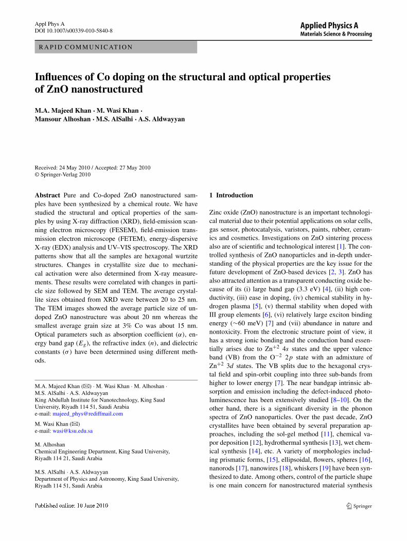
The XRD patterns of Zn1−xCoxO (x = 0, 0.01, 0.03 and0.05) samples sintered at the same temperature are shown inFig. 1. All the patterns are found to have hexagonal wurtzite
Fig. 1 XRD patterns of ZnO and Co-doped ZnO samples
structure, without any additional impurity phases, therebyindicating that the wurtzite structure might have not affecteddue to the substitution of Cobalt. Further, as no excess peakswere detected, it has been concluded that all the starting or-ganic precursors might have been completely decomposed.The 2θ values of the (101) peak have been observed in therange of 36.15◦–36.27◦. The addition of Co does not signifi-cant alter the diffraction angle and the full width at half max-imum (FWHM) value of the any observed peak, suggests theincorporation of Co ions into the ZnO matrix. The diffrac-tion peaks along with their relative intensities are found tobe in agreement with those from the others [20]. Further, theaverage crystallite size of all the samples were estimated us-ing a (101) peak broadening technique and are found to bein the range of 20–25 nm.
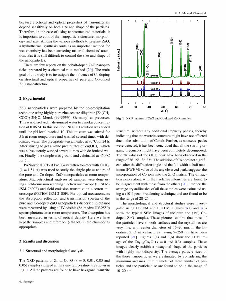
The morphological and structural studies were investi-gated using FESEM and FETEM. Figures 2(a) and 2(b)show the typical SEM images of the pure and (3%) Co-doped ZnO samples. These pictures exhibit that most ofthe particles have smooth surfaces and the crystallites arevery fine, with center diameters of 15–20 nm. In the lit-erature, ZnO nanostructures having 9–250 nm have beenreported [21]. Figures 3(a) and 3(b) show the TEM im-age of the Zn1−xCoxO (x = 0 and 0.3) samples. Theseimages clearly exhibit a hexagonal shape of the particleswith highly monodispersity. The average particle sizes ofthe these nanoparticles were estimated by considering theminimum and maximum diameter of large number of par-ticles and the particle size are found to be in the range of10–20 nm.
Influences of Co doping on the structural and optical properties of ZnO nanostructured
Fig. 2 FESEM micrographs of(a) pure ZnO and (b) (3%)Co-doped ZnO nanoparticles
Fig. 3 FETEM images of(a) pure ZnO and (b) (3%)Co-doped ZnO nanoparticles
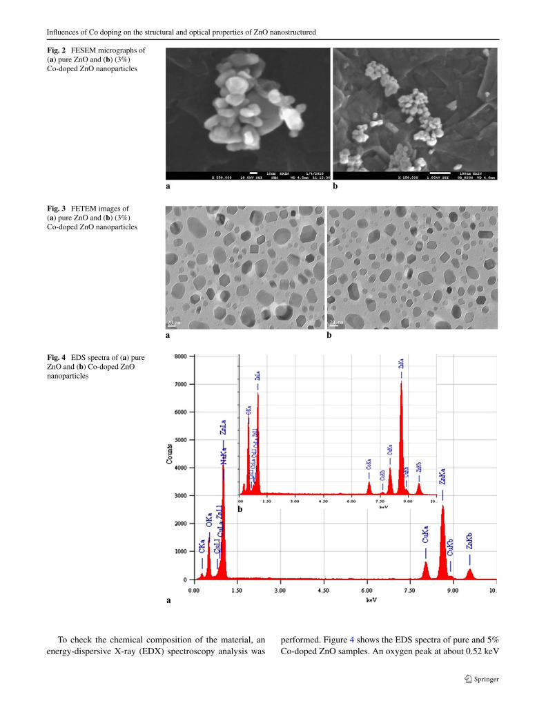
Fig. 4 EDS spectra of (a) pureZnO and (b) Co-doped ZnOnanoparticles
To check the chemical composition of the material, anenergy-dispersive X-ray (EDX) spectroscopy analysis was
performed. Figure 4 shows the EDS spectra of pure and 5%Co-doped ZnO samples. An oxygen peak at about 0.52 keV
M.A. Majeed Khan et al.
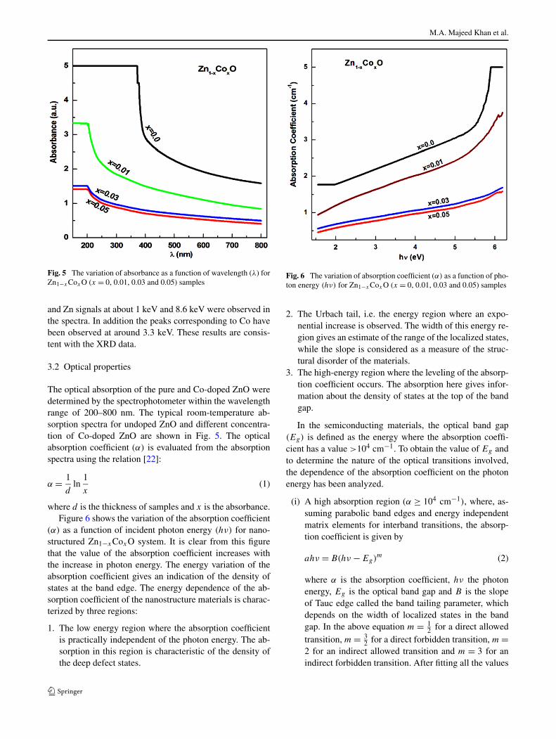
Fig. 5 The variation of absorbance as a function of wavelength (λ) forZn1−xCoxO (x = 0, 0.01, 0.03 and 0.05) samples
and Zn signals at about 1 keV and 8.6 keV were observed inthe spectra. In addition the peaks corresponding to Co havebeen observed at around 3.3 keV. These results are consis-tent with the XRD data.
3.2 Optical properties
The optical absorption of the pure and Co-doped ZnO weredetermined by the spectrophotometer within the wavelengthrange of 200–800 nm. The typical room-temperature ab-sorption spectra for undoped ZnO and different concentra-tion of Co-doped ZnO are shown in Fig. 5. The opticalabsorption coefficient (α) is evaluated from the absorptionspectra using the relation [22]:
α = 1
dln
1
x(1)
where d is the thickness of samples and x is the absorbance.Figure 6 shows the variation of the absorption coefficient
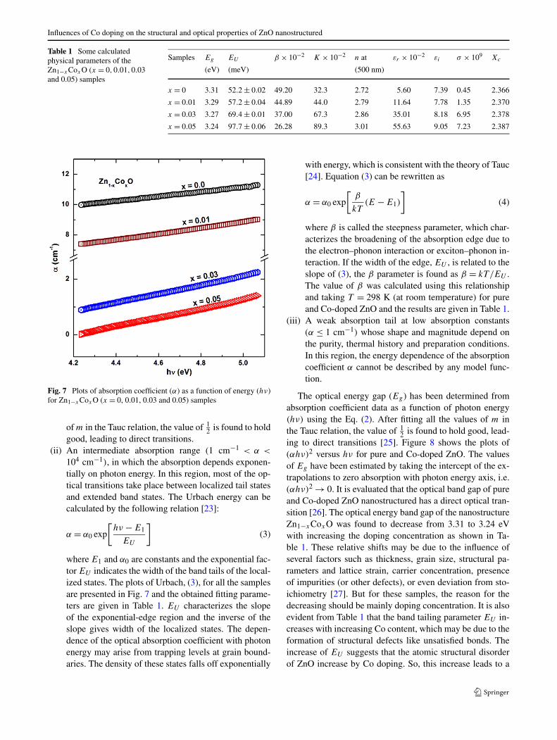
(α) as a function of incident photon energy (hν) for nano-structured Zn1−xCoxO system. It is clear from this figurethat the value of the absorption coefficient increases withthe increase in photon energy. The energy variation of theabsorption coefficient gives an indication of the density ofstates at the band edge. The energy dependence of the ab-sorption coefficient of the nanostructure materials is charac-terized by three regions:
1. The low energy region where the absorption coefficientis practically independent of the photon energy. The ab-sorption in this region is characteristic of the density ofthe deep defect states.
Fig. 6 The variation of absorption coefficient (α) as a function of pho-ton energy (hν) for Zn1−xCoxO (x = 0, 0.01, 0.03 and 0.05) samples
2. The Urbach tail, i.e. the energy region where an expo-nential increase is observed. The width of this energy re-gion gives an estimate of the range of the localized states,while the slope is considered as a measure of the struc-tural disorder of the materials.
3. The high-energy region where the leveling of the absorp-tion coefficient occurs. The absorption here gives infor-mation about the density of states at the top of the bandgap.
In the semiconducting materials, the optical band gap(Eg) is defined as the energy where the absorption coeffi-cient has a value >104 cm−1. To obtain the value of Eg andto determine the nature of the optical transitions involved,the dependence of the absorption coefficient on the photonenergy has been analyzed.
(i) A high absorption region (α ≥ 104 cm−1), where, as-suming parabolic band edges and energy independentmatrix elements for interband transitions, the absorp-tion coefficient is given by
ahν = B(hν − Eg)m (2)
where α is the absorption coefficient, hν the photonenergy, Eg is the optical band gap and B is the slopeof Tauc edge called the band tailing parameter, whichdepends on the width of localized states in the bandgap. In the above equation m = 1
2 for a direct allowedtransition, m = 3
2 for a direct forbidden transition, m =2 for an indirect allowed transition and m = 3 for anindirect forbidden transition. After fitting all the values
Influences of Co doping on the structural and optical properties of ZnO nanostructured
Table 1 Some calculatedphysical parameters of theZn1−xCoxO (x = 0,0.01,0.03and 0.05) samples
Samples Eg EU β × 10−2 K × 10−2 n at εr × 10−2 εi σ × 109 Xc
(eV) (meV) (500 nm)
x = 0 3.31 52.2 ± 0.02 49.20 32.3 2.72 5.60 7.39 0.45 2.366
x = 0.01 3.29 57.2 ± 0.04 44.89 44.0 2.79 11.64 7.78 1.35 2.370
x = 0.03 3.27 69.4 ± 0.01 37.00 67.3 2.86 35.01 8.18 6.95 2.378
x = 0.05 3.24 97.7 ± 0.06 26.28 89.3 3.01 55.63 9.05 7.23 2.387
Fig. 7 Plots of absorption coefficient (α) as a function of energy (hν)for Zn1−xCoxO (x = 0, 0.01, 0.03 and 0.05) samples
of m in the Tauc relation, the value of 12 is found to hold
good, leading to direct transitions.(ii) An intermediate absorption range (1 cm−1 < α <
104 cm−1), in which the absorption depends exponen-tially on photon energy. In this region, most of the op-tical transitions take place between localized tail statesand extended band states. The Urbach energy can becalculated by the following relation [23]:
α = α0 exp
[hν − E1
EU
](3)
where E1 and α0 are constants and the exponential fac-tor EU indicates the width of the band tails of the local-ized states. The plots of Urbach, (3), for all the samplesare presented in Fig. 7 and the obtained fitting parame-ters are given in Table 1. EU characterizes the slopeof the exponential-edge region and the inverse of theslope gives width of the localized states. The depen-dence of the optical absorption coefficient with photonenergy may arise from trapping levels at grain bound-aries. The density of these states falls off exponentially
with energy, which is consistent with the theory of Tauc[24]. Equation (3) can be rewritten as
α = α0 exp
[β
kT(E − E1)
](4)
where β is called the steepness parameter, which char-acterizes the broadening of the absorption edge due tothe electron–phonon interaction or exciton–phonon in-teraction. If the width of the edge, EU , is related to theslope of (3), the β parameter is found as β = kT /EU .The value of β was calculated using this relationshipand taking T = 298 K (at room temperature) for pureand Co-doped ZnO and the results are given in Table 1.
(iii) A weak absorption tail at low absorption constants(α ≤ 1 cm−1) whose shape and magnitude depend onthe purity, thermal history and preparation conditions.In this region, the energy dependence of the absorptioncoefficient α cannot be described by any model func-tion.
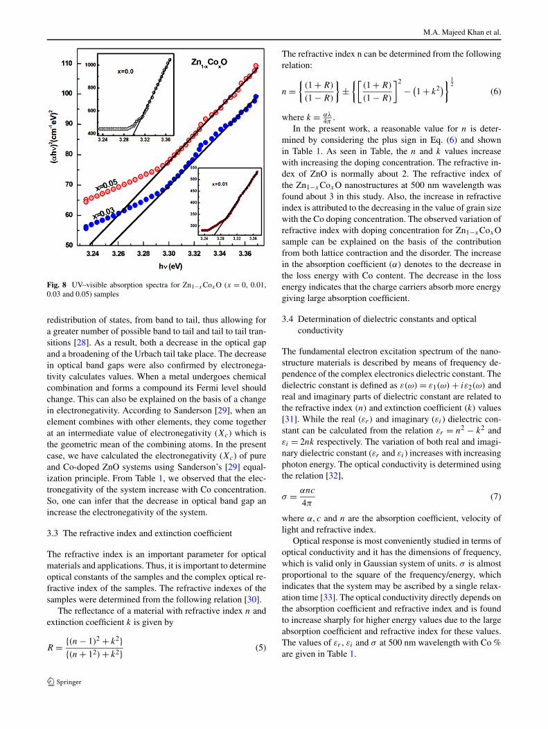
The optical energy gap (Eg) has been determined fromabsorption coefficient data as a function of photon energy(hν) using the Eq. (2). After fitting all the values of m inthe Tauc relation, the value of 1
2 is found to hold good, lead-ing to direct transitions [25]. Figure 8 shows the plots of(αhν)2 versus hν for pure and Co-doped ZnO. The valuesof Eg have been estimated by taking the intercept of the ex-trapolations to zero absorption with photon energy axis, i.e.(αhν)2 → 0. It is evaluated that the optical band gap of pureand Co-doped ZnO nanostructured has a direct optical tran-sition [26]. The optical energy band gap of the nanostructureZn1−xCoxO was found to decrease from 3.31 to 3.24 eVwith increasing the doping concentration as shown in Ta-ble 1. These relative shifts may be due to the influence ofseveral factors such as thickness, grain size, structural pa-rameters and lattice strain, carrier concentration, presenceof impurities (or other defects), or even deviation from sto-ichiometry [27]. But for these samples, the reason for thedecreasing should be mainly doping concentration. It is alsoevident from Table 1 that the band tailing parameter EU in-creases with increasing Co content, which may be due to theformation of structural defects like unsatisfied bonds. Theincrease of EU suggests that the atomic structural disorderof ZnO increase by Co doping. So, this increase leads to a
M.A. Majeed Khan et al.
Fig. 8 UV–visible absorption spectra for Zn1−xCoxO (x = 0, 0.01,0.03 and 0.05) samples
redistribution of states, from band to tail, thus allowing fora greater number of possible band to tail and tail to tail tran-sitions [28]. As a result, both a decrease in the optical gapand a broadening of the Urbach tail take place. The decreasein optical band gaps were also confirmed by electronega-tivity calculates values. When a metal undergoes chemicalcombination and forms a compound its Fermi level shouldchange. This can also be explained on the basis of a changein electronegativity. According to Sanderson [29], when anelement combines with other elements, they come togetherat an intermediate value of electronegativity (Xc) which isthe geometric mean of the combining atoms. In the presentcase, we have calculated the electronegativity (Xc) of pureand Co-doped ZnO systems using Sanderson’s [29] equal-ization principle. From Table 1, we observed that the elec-tronegativity of the system increase with Co concentration.So, one can infer that the decrease in optical band gap anincrease the electronegativity of the system.
3.3 The refractive index and extinction coefficient
The refractive index is an important parameter for opticalmaterials and applications. Thus, it is important to determineoptical constants of the samples and the complex optical re-fractive index of the samples. The refractive indexes of thesamples were determined from the following relation [30].
The reflectance of a material with refractive index n andextinction coefficient k is given by
R = {(n − 1)2 + k2}{(n + 12) + k2} (5)
The refractive index n can be determined from the followingrelation:
n ={
(1 + R)
(1 − R)
}±
{[(1 + R)
(1 − R)
]2
− (1 + k2)} 1
2
(6)
where k = αλ4π
.In the present work, a reasonable value for n is deter-
mined by considering the plus sign in Eq. (6) and shownin Table 1. As seen in Table, the n and k values increasewith increasing the doping concentration. The refractive in-dex of ZnO is normally about 2. The refractive index ofthe Zn1−xCoxO nanostructures at 500 nm wavelength wasfound about 3 in this study. Also, the increase in refractiveindex is attributed to the decreasing in the value of grain sizewith the Co doping concentration. The observed variation ofrefractive index with doping concentration for Zn1−xCoxOsample can be explained on the basis of the contributionfrom both lattice contraction and the disorder. The increasein the absorption coefficient (α) denotes to the decrease inthe loss energy with Co content. The decrease in the lossenergy indicates that the charge carriers absorb more energygiving large absorption coefficient.
3.4 Determination of dielectric constants and opticalconductivity
The fundamental electron excitation spectrum of the nano-structure materials is described by means of frequency de-pendence of the complex electronics dielectric constant. Thedielectric constant is defined as ε(ω) = ε1(ω) + iε2(ω) andreal and imaginary parts of dielectric constant are related tothe refractive index (n) and extinction coefficient (k) values[31]. While the real (εr ) and imaginary (εi ) dielectric con-stant can be calculated from the relation εr = n2 − k2 andεi = 2nk respectively. The variation of both real and imagi-nary dielectric constant (εr and εi ) increases with increasingphoton energy. The optical conductivity is determined usingthe relation [32],
σ = αnc
4π(7)
where α, c and n are the absorption coefficient, velocity oflight and refractive index.
Optical response is most conveniently studied in terms ofoptical conductivity and it has the dimensions of frequency,which is valid only in Gaussian system of units. σ is almostproportional to the square of the frequency/energy, whichindicates that the system may be ascribed by a single relax-ation time [33]. The optical conductivity directly depends onthe absorption coefficient and refractive index and is foundto increase sharply for higher energy values due to the largeabsorption coefficient and refractive index for these values.The values of εr , εi and σ at 500 nm wavelength with Co %are given in Table 1.
Influences of Co doping on the structural and optical properties of ZnO nanostructured
4 Conclusions
In summary, the structural and optical properties of pure andCo-doped ZnO nanostructured have been investigated. Theformation of Zn1−xCoxO nanoparticles of ∼20 nm size withhexagonal wurtzite structure has been observed by TEM andXRD. The optical band gap and optical constants (refrac-tive index, extinction coefficient) of pure and Co-doped ZnOnanostructured were determined. Increasing the Co contentleads to a decrease of the optical gap and increases the widthof localized states, which indicates that Co substitution in-troduces a narrow band of disorder states at band edges. Thedielectric constants and optical conductivity are determinedfor the system and they are found to follow a similar trendas that of the refractive index.
Acknowledgements The authors are grateful to the King AbdullahInstitute for Nanotechnology, for supporting this work. Author M. WasiKhan is thankful to Dr. Mohd. Aslam Khan (KAIN) for his help inexperiments.
References
1. K.F. Cai, X.R. He, L.C. Zhang, Mater. Lett. 62, 1223 (2008)2. C.L. Dong, C. Persson, L. Vayssieres, A. Augustsson, T. Schmitt,
M. Mattesini, R. Ahuja, C.L. Chang, J.H. Guo, Phys. Rev. B 70,195325 (2004)
3. M. Huang, S. Mao, H. Feick, H. Yan, Y. Wu, H. Kind, E. Weber,R. Russo, P. Yang, Science 292, 18979 (2001)
4. Y. Zhu, Y. Chen, X. Zhang, Q. Chen, Y. Shao, Mater. Lett. 63,1242 (2009)
5. S. Major, A. Banerjee, K.L. Chopra, Thin Solid Films 108, 333(1983)
6. T.L. Tansley, D.F. Neely, C.P. Foley, Thin Solid Films 117, 19(1984)
7. U. Ozgur, Ya.I. Alivov, C. Liu, A. Teke, M. Reshchikov, S. Dogan,V. Avrutin, S.J. Cho, H. Morkoç, J. Appl. Phys. 98, 041301 (2005)
8. A.F. Kohan, G. Ceder, D. Morgan, C.G. Van de Walle, Phys. Rev.B 61, 15019 (2000)
9. B. Kumar, H. Gong, S. Vicknesh, S.J. Chua, S. Tripathy, Appl.Phys. Lett. 89, 141901 (2006)
10. P. Misra, T.K. Sharma, S. Porwal, L.M. Kukreja, Appl. Phys. Lett.89, 161912 (2006)
11. S. Rani, P. Puri, P.K. Shisodia, R.M. Mehra, Sol. Energy Mater.Sol. Cells 92(12), 1639 (2008)
12. D. Shuang, J.B. Wang, X.L. Zhong, H.L. Yan, Mater. Sci. Semi-cond. Process. 10, 97 (2007)
13. Y.-H. Ni, X.-W. Wei, J.-M. Hong, Y. Ye, Mater. Sci. Eng. B 121,42 (2005)
14. S.-H. Hu, Y.-C. Chen, C.-C. Hwang, C.-H. Peng, D.-C. Gong, Y.Ye, J. Alloys Compd. 500, L17 (2010)
15. J. Zhao, Z.-G. Jin, X.-X. Liu, Z.-F. Liu, J. Eur. Ceram. Soc. 26,3745 (2006)
16. J. Liu, X. Huang, Y. Li, Q. Zhong, L. Ren, Mater. Lett. 60, 1354(2006)
17. T. Mahalingam, K.M. Lee, K.H. Park, S. Lee, Y. Ahn, J.-Y. Park,K.H. Koh, Nanotechnology 18, 035606 (2007)
18. Y. Sun, N.G. Ndifor-Angwafor, R.D. Jason, N.R.M. Ashfold,Chem. Phys. Lett. 431, 352 (2006)
19. R. Wu, Y. Yang, S. Cong, Z. Wu, C. Xie, H. Usui, K. Kawaguchi,N. Koshizaki, Chem. Phys. Lett. 406, 457 (2005)
20. E.J. Luna-Arredondo, A. Maldonado, R. Asomoza, D.R. Acosta,M.A. Melendez-Lira, M. de la L. Olvera, Thin Solid Films 490,132 (2005)
21. S. Mridha, D. Basak, Mater. Res. Bull. 42, 875 (2007)22. R. Swanepoel, J. Phys. E, Sci. Instrum. 16, 1214 (1983)23. F. Urbach, Phys. Rev. 92, 1324 (1953)24. J. Tauc, Amorphous and Liquid Semiconductors (Plenum, New
York, 1974)25. J. Tauc, The Optical Properties of Solids (North-Holland, Amster-
dam, 1970)26. U.N. Maiti, P.K. Ghosh, S. Nandy, K.K. Chattopadhyay, Physica
B 387, 103 (2007)27. T. Ren, H.R. Baker, K.M. Poduska, Thin Solid Films 515, 7976
(2007)28. M. Caglar, S. Ilican, Y. Caglar, Thin Solid Films 517, 5023 (2009)29. R.T. Sanderson, Inorganic Chemistry (East-West Press PUT, New
Delhi, 1971)30. N.A. Subrahamanyam, A Textbook of Optics (Brij Laboratory,
Delhi, 1977)31. M.M. Wakkad, E.Kh. Shoker, S.H. Mohamed, J. Non-Cryst.
Solids 265, 157 (2000)32. S.H. Wemple, M. DiDomenico, Phys. Rev. B 3, 1338 (1971)33. K. Shimakawa, S. Narushima, S. Hosono, H. Kawazoe, Philos.
Mag. Lett. 79, 755 (1999)