Comparative effects of indium/ytterbium doping on, mechanical and gas-sensitivity-related...
6
Journal of Alloys and Compounds 501 (2010) 339–344 Contents lists available at ScienceDirect Journal of Alloys and Compounds journal homepage: www.elsevier.com/locate/jallcom Comparative effects of indium/ytterbium doping on, mechanical and gas-sensitivity-related morphological, properties of sprayed ZnO compounds A. Boukhachem a , S. Fridjine a , A. Amlouk a , K. Boubaker a,∗ , M. Bouhafs b , M. Amlouk a a Unité de physique des dispositifs à semi-conducteurs, Faculté des sciences de Tunis, Université de Tunis El Manar, 2092 Tunis, Tunisia b Unité de Recherche MA2I, ˙ Ecole Nationale d’Ingénieurs de Tunis B.P. 37, Le Belvédère, 1002 Tunis, Tunisia article info Article history: Received 15 January 2010 Received in revised form 7 April 2010 Accepted 14 April 2010 Available online 24 April 2010 PACS: 2008: 77.84.Bw 81.15.Rs 81.40.Ef 84.60.Jt Keywords: Zinc oxide Opto-thermal expansivity AB Surface roughness Indium doping Optical properties BPES Ytterbium doping abstract In this study, conducting and transparent indium-doped zinc oxide (ZnO) thin films have been deposited on glass substrates by the micro-spray technique. First, zinc oxide layers were obtained by spaying a solution of propanol and zinc acetate in acidified medium. Alternatively, some of the obtained films were doped with indium (In) at the molar rates of: 1%, 2% and 3%. In addition to the classical structural investigated using XRD, AFM and SEM techniques, microhardness Vickers (Hv) measurements have been carried out along with comparative morphological prospecting. The specific gases sensitivity-related surface morphology of the doped ZnO compounds was favorably different from that of the non-doped ones, and showed a thin overlay structure. Results were compared to those recorded for similar ytterbium-doped material. © 2010 Elsevier B.V. All rights reserved. 1. Introduction Zinc oxide (ZnO) is a hexagonal würtzite structured semicon- ductor with high piezoelectric and gas-detecting properties [1–7]. Its deposition on polymer substrates has been widely discussed and exploited in the last four decades literature [6–11]. Recently, it has been established that polymers, although having merits of being cheaper and lighter than glass-similar materials, present a higher thermal diffusivity and besides all a weaker mechanical strength. Consequently, glass has been preferred as substrate in the major part of recent applications. On another hand, the structure and the mechanical performance of the active ZnO layer could not be improved accordingly. Many attempts have been made in this context. In a lastly carried out investigation [12], an accidental ytterbium doping suggested new routes for hardening such binary structures. This trend was motivated by a recent orientation toward a mean- ∗ Corresponding author. E-mail address: [email protected] (K. Boubaker). ingful contribution of the active layers to the mechanical resistance of the whole sensing devices which are more and more subjected to external solicitations and constraints. In recent studies, many doping elements for ZnO have been experimented [13–16]. In some studies, the merits of indium as an effective doping agent have been pointed out. Nevertheless, there is a lack of information about the way indium affects ZnO compounds roughness and crystal parameters physical parameters. In this work, explanations to the paradoxical effects of indium doping at macro and micro levels are presented. Doping techniques and processes have been detailed along with common characteriz- ing means. The last part of this paper is dedicated to the nano-scale analyses and discussions. 2. Experimental details 2.1. Indium-free and indium-doped ZnO films preparation Indium-free ZnO thin films have been first prepared in a glass substrate tem- perature domain of 400–500 ◦ C with a mean value of 460 ± 5 ◦ C [17], using propanol and zinc Acetate (Zn(CH3CO2)2):10 −2 M according to the chemical protocol sum- marized in Fig. 1. Indeed, ethanol and water were used previously [12,17] but the iso-propyl alcohol has been tested as the best to dissolve the zinc acetate and to gives acceptable adherence of ZnO thin films on glass substrate. 0925-8388/$ – see front matter © 2010 Elsevier B.V. All rights reserved. doi:10.1016/j.jallcom.2010.04.100
-
Upload
independent -
Category
Documents
-
view
0 -
download
0
Transcript of Comparative effects of indium/ytterbium doping on, mechanical and gas-sensitivity-related...
Cg
Aa
b
a
ARRAA
P2888
KZOSIOBY
1
dIebctCp
oa
dT
0d
Journal of Alloys and Compounds 501 (2010) 339–344
Contents lists available at ScienceDirect
Journal of Alloys and Compounds
journa l homepage: www.e lsev ier .com/ locate / ja l l com
omparative effects of indium/ytterbium doping on, mechanical andas-sensitivity-related morphological, properties of sprayed ZnO compounds
. Boukhachema, S. Fridjinea, A. Amlouka, K. Boubakera,∗, M. Bouhafsb, M. Amlouka
Unité de physique des dispositifs à semi-conducteurs, Faculté des sciences de Tunis, Université de Tunis El Manar, 2092 Tunis, TunisiaUnité de Recherche MA2I, Ecole Nationale d’Ingénieurs de Tunis B.P. 37, Le Belvédère, 1002 Tunis, Tunisia
r t i c l e i n f o
rticle history:eceived 15 January 2010eceived in revised form 7 April 2010ccepted 14 April 2010vailable online 24 April 2010
ACS:008: 77.84.Bw1.15.Rs1.40.Ef4.60.Jt
a b s t r a c t
In this study, conducting and transparent indium-doped zinc oxide (ZnO) thin films have been depositedon glass substrates by the micro-spray technique. First, zinc oxide layers were obtained by spaying asolution of propanol and zinc acetate in acidified medium. Alternatively, some of the obtained filmswere doped with indium (In) at the molar rates of: 1%, 2% and 3%. In addition to the classical structuralinvestigated using XRD, AFM and SEM techniques, microhardness Vickers (Hv) measurements have beencarried out along with comparative morphological prospecting.
The specific gases sensitivity-related surface morphology of the doped ZnO compounds was favorablydifferent from that of the non-doped ones, and showed a thin overlay structure. Results were comparedto those recorded for similar ytterbium-doped material.
© 2010 Elsevier B.V. All rights reserved.
eywords:inc oxidepto-thermal expansivity AB
urface roughnessndium dopingptical properties
PEStterbium doping. Introduction
Zinc oxide (ZnO) is a hexagonal würtzite structured semicon-uctor with high piezoelectric and gas-detecting properties [1–7].
ts deposition on polymer substrates has been widely discussed andxploited in the last four decades literature [6–11]. Recently, it haseen established that polymers, although having merits of beingheaper and lighter than glass-similar materials, present a higherhermal diffusivity and besides all a weaker mechanical strength.onsequently, glass has been preferred as substrate in the majorart of recent applications.
On another hand, the structure and the mechanical performancef the active ZnO layer could not be improved accordingly. Many
ttempts have been made in this context.In a lastly carried out investigation [12], an accidental ytterbiumoping suggested new routes for hardening such binary structures.his trend was motivated by a recent orientation toward a mean-
∗ Corresponding author.E-mail address: [email protected] (K. Boubaker).
925-8388/$ – see front matter © 2010 Elsevier B.V. All rights reserved.oi:10.1016/j.jallcom.2010.04.100
ingful contribution of the active layers to the mechanical resistanceof the whole sensing devices which are more and more subjectedto external solicitations and constraints.
In recent studies, many doping elements for ZnO have beenexperimented [13–16]. In some studies, the merits of indium as aneffective doping agent have been pointed out. Nevertheless, there isa lack of information about the way indium affects ZnO compoundsroughness and crystal parameters physical parameters.
In this work, explanations to the paradoxical effects of indiumdoping at macro and micro levels are presented. Doping techniquesand processes have been detailed along with common characteriz-ing means. The last part of this paper is dedicated to the nano-scaleanalyses and discussions.
2. Experimental details
2.1. Indium-free and indium-doped ZnO films preparation
Indium-free ZnO thin films have been first prepared in a glass substrate tem-perature domain of 400–500 ◦C with a mean value of 460 ± 5 ◦C [17], using propanoland zinc Acetate (Zn(CH3CO2)2):10−2 M according to the chemical protocol sum-marized in Fig. 1. Indeed, ethanol and water were used previously [12,17] but theiso-propyl alcohol has been tested as the best to dissolve the zinc acetate and togives acceptable adherence of ZnO thin films on glass substrate.
340 A. Boukhachem et al. / Journal of Alloys an
pZ(i
tf
dvm
etps
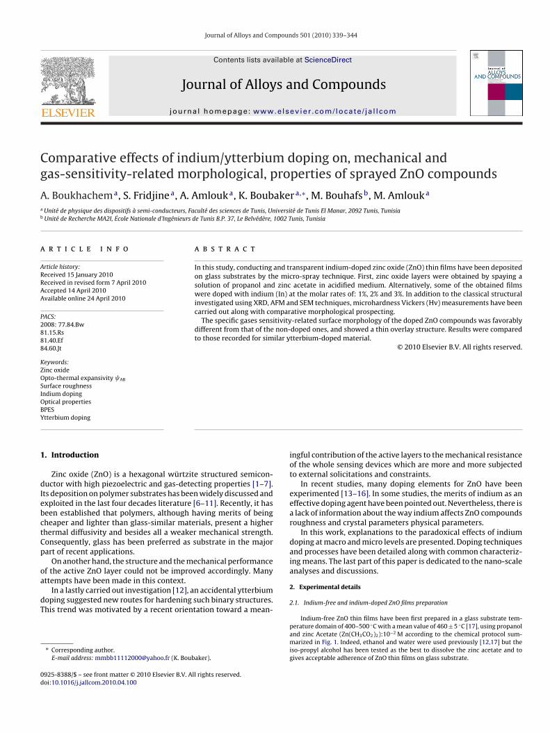
Fig. 1. Zno layers elaboration chemical protocol.
In the beginning of the process, dissolution process involves a sim-le liquid–liquid dissolution along with a chemical reaction yielding bothn4O(CH3CO2)6 and CH3CO. At an intermediary stage, the three compoundsZn4O(CH3CO2)6, (Zn(CH3CO2)2) and CH3CO) yield evaporated gases and a remain-ng layered compound (ZnO).
The precursor mixture was acidified using acetic acid (pH 5), the obtained ZnOhin films’ thickness was approximately 0.5 �m. These films are designated, in theollowing parts of the study, as (A) or In-free samples.
Nitrogen was used as the carrier gas (pressure at 0.35 bar) through a 0.5 mm-iameter nozzle. The nozzle-to-substrate plane distance was fixed at the optimalalue of 27 cm as demonstrated by Boubaker et al. [18]. During deposition, precursorixture flow rate was held constant at 4 mL/min.
Indium-doped ZnO:In thin films solution have been fabricated under the samexperimental conditions, by adding indium chloride (InCl3, xH2O, 99.9% purity) tohe precursor solution while maintaining acidity level. In the three elaborated sam-les, the indium-to-zinc molar ratio: In3+/Zn2+ was 1, 2 and 3%. The correspondingamples were designated as (B), (C) and (D), respectively.
Fig. 2. As-grown layers 3D
d Compounds 501 (2010) 339–344
2.2. Common characterization techniques
Samples (A), (B), (C) and (D) 3D surface topography was examined by atomicforce microscopy (AFM) using a VEECO digital instrument 3A microscope in con-tact mode. Then, the samples films were investigated using X-ray diffractometry bymeans of a Philips (PW1429) system. The optical transmittance T (�) and reflectanceR (�) of the films were recorded using a Schimadzu UV 3100 double-beam spec-trophotometer, within a (300–1800 nm) wavelength range.
Finally, a thorough mechanical characterization was carried out using adiamond-pyramidal-indenter Vickers test disposal which is deeply detailed inprecedent studies [19,20].
3. Characterization
3.1. Atomic force microscopy (AFM) microanalysis
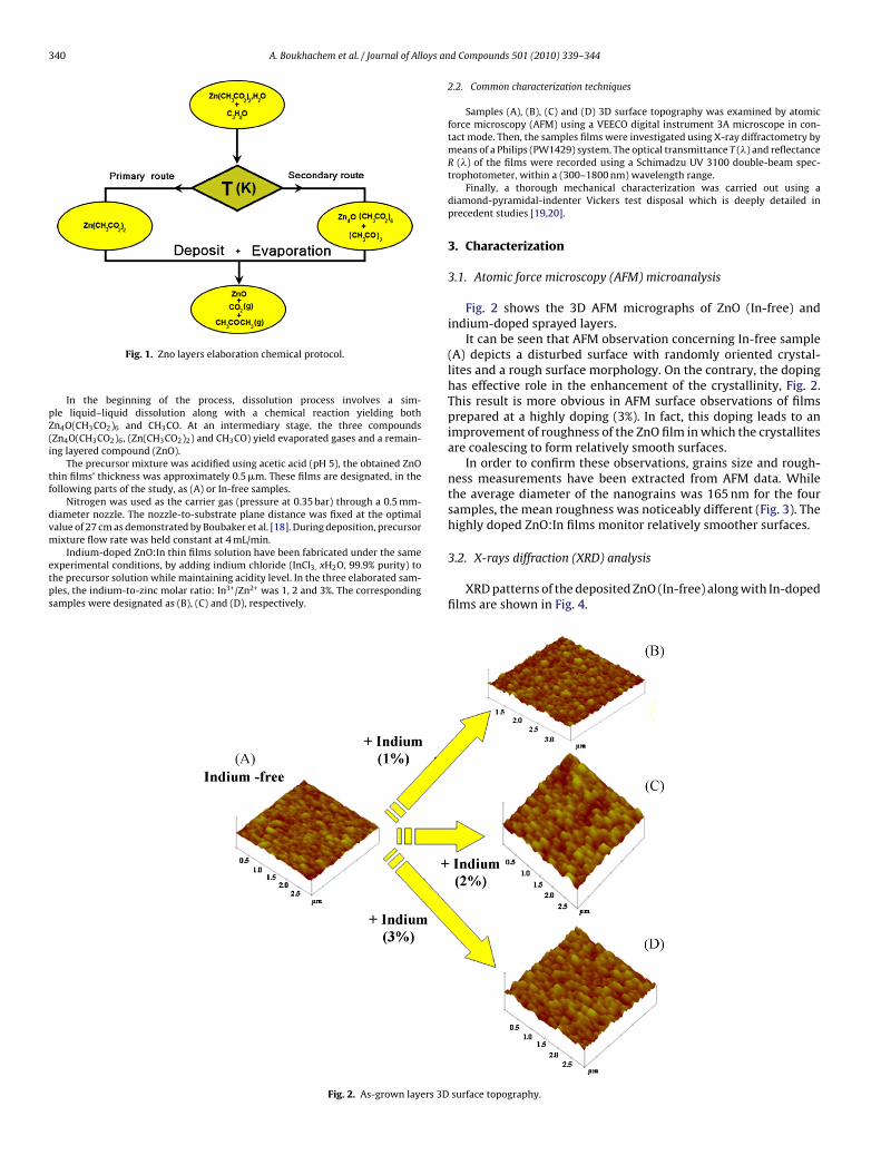
Fig. 2 shows the 3D AFM micrographs of ZnO (In-free) andindium-doped sprayed layers.
It can be seen that AFM observation concerning In-free sample(A) depicts a disturbed surface with randomly oriented crystal-lites and a rough surface morphology. On the contrary, the dopinghas effective role in the enhancement of the crystallinity, Fig. 2.This result is more obvious in AFM surface observations of filmsprepared at a highly doping (3%). In fact, this doping leads to animprovement of roughness of the ZnO film in which the crystallitesare coalescing to form relatively smooth surfaces.
In order to confirm these observations, grains size and rough-ness measurements have been extracted from AFM data. Whilethe average diameter of the nanograins was 165 nm for the foursamples, the mean roughness was noticeably different (Fig. 3). Thehighly doped ZnO:In films monitor relatively smoother surfaces.
3.2. X-rays diffraction (XRD) analysis
XRD patterns of the deposited ZnO (In-free) along with In-dopedfilms are shown in Fig. 4.
surface topography.
A. Boukhachem et al. / Journal of Alloys and Compounds 501 (2010) 339–344 341
Fo
drg((eaaaap
3
3
s
tt
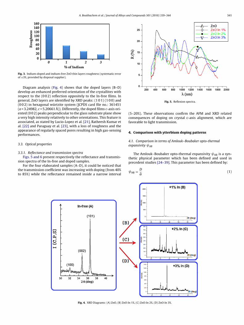
ig. 3. Indium-doped and indium-free ZnO thin layers roughness (systematic errorf ±3%, provided by disposal supplier).
Diagram analysis (Fig. 4) shows that the doped layers (B–D)evelop an enhanced preferred orientation of the crystallites withespect to the (0 0 2) reflection oppositely to the In-free films. Ineneral, ZnO layers are identified by XRD peaks: (1 0 1) (1 0 0) and0 0 2) in hexagonal würtzite system (JCPDS card file no.: 361451a = 3.24982, c = 5.20661 Å)). Differently, the doped films c-axis ori-nted (0 0 2) peaks perpendicular to the glass substrate plane showvery high intensity relatively to other orientations. This feature isssociated, as stated by Lucio-Lopez et al. [21], Ratheesh Kumar etl. [22] and Paraguay et al. [23], with a loss of roughness and theppearance of regularly spaced pores resulting in high gas-sensingerformances.
.3. Optical properties
.3.1. Reflectance and transmission spectra
Figs. 5 and 6 present respectively the reflectance and transmis-ion spectra of the In-free and doped samples.For the four elaborated samples (A–D), it could be noticed that
he transmission coefficient was increasing with doping (from 40%o 85%) while the reflectance remained inside a narrow interval
Fig. 4. XRD Diagrams: (A) ZnO, (B) ZnO:I
Fig. 5. Reflexion spectra.
(5–20%). These observations confirm the AFM and XRD relatedconsequences of doping on crystal c-axis alignment, which arefavorable to light transmission.
4. Comparison with ytterbium doping patterns
4.1. Comparison in terms of Amlouk–Boubaker opto-thermalexpansivity AB
The Amlouk–Boubaker opto-thermal expansivity AB is a syn-
thetic physical parameter which has been defined and used inprecedent studies [24–39]. This parameter has been defined by:AB = D
ˆ(1)
n 1%, (C) ZnO:In 2%, (D) ZnO:In 3%.
342 A. Boukhachem et al. / Journal of Alloys an
Fig. 6. Transmission spectra.
Table 1Values of the Amlouk–Boubaker opto-thermal expansivity.
Sample AB (m3 s−1)
Yb-doped ZnO 0 ppm 18.2 × 10⁻¹²
100 ppm 14.5 × 10⁻¹²
200 ppm 12.9 × 10⁻¹²
300 ppm 10.1 × 10⁻¹²
In-doped ZnO 0% 18.2 × 10⁻¹²
1% 9.21 × 10⁻¹²
wa
ni
˛bium and indium doped layers, has been evaluated in terms ofVickers Hardness (Hv). The characterization test has been carried
2% 8.24 × 10⁻¹²
3% 11.2 × 10⁻¹²
here D is the thermal diffusivity and ˆ is the effectivebsorptivity.
The effective absorptivity ˆ , is defined [30–33] as the meanormalized absorbance weighted by I(�)AM1.5, the solar standard
rradiance, with �: the normalized wavelength:
ˆ =
1∫0
I(�)AM1.5 × ˛(�)d�
1(2)
∫0
I(�)AM1.5d�
Fig. 7. Vickers Hardness
d Compounds 501 (2010) 339–344
and where: I(�)AM1.5 is the reference solar spectral irradiance, fittedusing the Boubaker polynomials expansion scheme, BPES.
4.1.1. Determination of the effective absorptivity ˆ using the BPESThe normalized absorbance spectrum ˛(�) is deduced from
the BPES. According to this protocol: a set of m experi-mental measured values of the transmittance-reflectance vec-tor
(Ti(�i);Ri(�i)
)∣∣i=1,...,m
versus the normalized wavelength
�i∣∣i=1,...,m
is established. Then the system (3) is set:⎧⎪⎪⎪⎪⎪⎪⎪⎪⎪⎪⎪⎪⎨⎪⎪⎪⎪⎪⎪⎪⎪⎪⎪⎪⎪⎩
R(�) =[
12N0
N0∑n=1
�n × B4n(�× ˇn)
]
T(�) =[
12N0
N0∑n=1
�′n × B4n(�× ˇn)
]
˛(�) = 1
d√
2
√√√√(ln1 − R(�)
T(�)
)2
+(
ln
(1 − R(�)
)2
T(�)
)2
(3)
whereˇn are the 4n-Boubaker polynomials B4n minimal positiveroots [30], N0 is a given integer, d is the layer thickness and �n and�
′n are coefficients determined through BPES.
The effective absorptivity ˆ is then calculated using Eq. (2).
4.1.2. Determination of Amlouk–Boubaker opto-thermalexpansivity AB
The calculated values of the Amlouk–Boubaker opto-thermalexpansivity AB, for the ytterbium and indium-doped layers aregathered in Table 1.
This result is in agreement with those of XRD and AFM describedabove. The increasing c-axis oriented (0 0 2) alignment of ZnO crys-tallites seems to have positive effects on opto-thermal propertiesof these doped films via a decrease of AB.
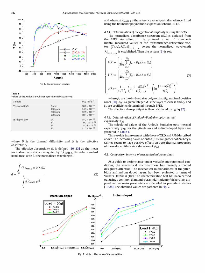
4.2. Comparison in terms of mechanical microhardness
As a guide to performance under variable environmental con-ditions, the mechanical microhardness has recently attracteddesigner’s attention. The mechanical microhardness of the ytter-
out using a common diamond-pyramidal-indenter Vickers test dis-posal whose main parameters are detailed in precedent studies[19,28]. The obtained values are gathered in Fig. 7.
of the doped films.
A. Boukhachem et al. / Journal of Alloys an
yif
4
t(irih(
iodciTcbcintu1ae
ttaitpTm
5
spa
[[[
[[[
[[[
[[
[
[
[
[
[[
[
[
[[[[[[
[[[[[[[[
[[
[
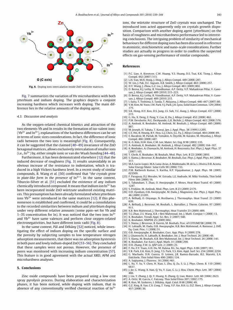
Fig. 8. Doping ions intercalation inside ZnO würtzite matrices.
Fig. 7 summarizes the variation of Hv microhardness with bothtterbium and indium doping. The graphics depicts a conjointncreasing hardness which increases with doping. The main dif-erence lies in the relative amounts of the doping agent.
.3. Discussion and analysis
As the oxygen-related chemical kinetics and attraction of thewo elements Yb and In results in the formation of iso-valent ions:Yb3+ and In3+), explanations of the hardness differences can be setn terms of ionic sizes considerations. In fact, the difference of ionicadii between the two ions is meaningful (Fig. 8). Consequently,t can be suggested that the claimed [40–49] invariance of the ZnOexagonal matrices, allows exclusively intercalation of smaller ionsi.e., In3+) by, either simple ionic or van der Waals bonding [44–48].
Furthermore, it has been demonstrated elsewhere [12] that thenduced decrease of roughness (Fig. 3) results unavoidably in anbvious increase of the resistance to indentation, which is tra-uced in a high Vickers hardness level. In a recent study of similarompounds, B. Wang et al. [50] confirmed that “the crystals grown plate-like form in the presence of In3+”. In the same context,iburcio-Silver et al. [51] excluded the existence of any indiumhemically introduced compound. It means that indium ion In3+ haseen incorporated inside ZnO würtzute unaltered existing matri-es. This presumption has been already formulated when ytterbiumons Yb3+ were introduced in the same matrices [12]. If this phe-omenon is established and confirmed, it could be a consolidationo the recorded similarities between indium and ytterbium dopingnder very different relative amounts (some ppm–wt for Yb and–3% concentration for In). It was noticed that the two ions In3+
nd Yb3+ have same valences and perform close oxygen-relatedlectronegativities, but have different ionic radii (Fig. 8).
In the same context, Pál and Dékány [52] noticed, while inves-igating the effect of indium doping on the specific surface andhe porosity by subjecting samples to low temperature nitrogendsorption measurements, that there was no adsorption hysteresisn both pure and lowly indium-doped ZnO [53–56]. They concludedhat these samples were not porous. However, the presence ofores was monitored with increasing indium concentration [57].his feature is in good agreement with the actual XRD, AFM andicrohardness analyses.
. Conclusions
Zinc oxide compounds have been prepared using a low costpray pyrolysis process. During elaboration and characterizationhases, it has been noticed, while doping with indium, that inbsence of any conventionally verified chemical reaction of In3+
[[[[
d Compounds 501 (2010) 339–344 343
ions, the würtzite structure of ZnO crystals was unchanged. Theintroduced ions acted apparently only on crystals growth dispo-sition. Comparison with another doping agent (ytterbium) on thebasis of roughness and microhardness performance led to interest-ing conclusions. The intriguing problem of similarity of mechanicalbehaviours for different doping ions has been discussed in referenceto atomistic, stoichiometric and nano-scale considerations. Furtherstudies are actually in progress in order to confirm the suspectedeffects on gas-sensing performance of similar compounds.
References
[1] P.C. Liao, A. Korotcov, C.W. Huang, Y.S. Huang, D.S. Tsai, K.K. Tiong, J. AlloysCompd. 442 (2007) 313.
[2] L.H. Van, M.H. Hong, J. Ding, J. Alloys Compd. 449 (2008) 207.[3] W. Lin, J. Pak, D.C. Ingram, A.R. Smith, J. Alloys Compd. 463 (2008) 257.[4] D.Y. Wang, J. Zhou, G.Z. Liu, J. Alloys Compd. 481 (2009) 802.[5] D. Beena, K.J. Lethy, R. Vinodkumar, A.P. Detty, V.P. Mahadevan Pillai, V. Gane-
san, J. Alloys Compd. 489 (2010) 215–223.[6] D. Beena, K.J. Lethy, R. Vinodkumar, A.P. Detty, V.P. Mahadevan Pillai, V. Gane-
san, J. Alloys Compd. 489 (2010) 215.[7] I. Saita, T. Toshima, S. Tanda, T. Akiyama, J. Alloys Compd. 446–447 (2007) 80.[8] Y.M. Kim, M. Yoon, I.W. Park, Y.J. Park, J.H. Lyou, Solid State Commun. 129 (2004)
175.[9] S.K. Hong, H.Y. Koo, D.S. Jung, I.S. Suh, Y.C. Kang, J. Alloys Compd. 437 (2008)
215.10] G. Hu, X. Deng, Z. Peng, Y. Cao, K. Du, J. Alloys Compd. 452 (2008) 462.11] P.M. Devshette, N.G. Deshpande, G.K. Bichile, J. Alloys Compd. 463 (2008) 576.12] A. Amlouk, K. Boubaker, M. Amlouk, M. Bouhafs, J. Alloys Compd. 485 (2009)
887.13] M. Joseph, H. Tabata, T. Kawai, Jpn. J. Appl. Phys. 38 (1999) L1205.14] C.S. Hsi, B. Houng, B.Y. Hou, G.J. Chen, S.L. Fu, J. Alloys Compd. 464 (2008) 89.15] E. Bacaksiz, M. Parlak, M. Tomakin, A. Özcelik, M. Karakız, M. Altunbas, J. Alloys
Compd. 466 (2008) 447.16] K.-S. Kim, H.W. Kim, C.M. Lee, Mater. Sci. Eng. B 98 (2003) 135.17] A. Amlouk, K. Boubaker, M. Amlouk, J. Alloys Compd. 482 (2009) 164–167.18] K. Boubaker, A. Chaouachi, M. Amlouk, H. Bouzouita, Eur. Phys. J. Appl. Phys. 37
(2007) 105.19] T. Ghrib, K. Boubaker, M. Bouhafs, Mod. Phys. Lett. B 22 (2008) 2893.20] S. Slama, J. Bessrour, K. Boubaker, M. Bouhafs, Eur. Phys. J. Appl. Phys. 44 (2008)
317.21] M.A. Lucio-Lopez, M.A. Luna-Arias, A. Maldonado, M. de la, L. Olvera, D.R. Acosta,
Solar Energy Mater. Solar Cells 90 (2006) 733.22] P.M. Ratheesh Kumar, S. Kartha, K.P. Vijayakumar, J. Appl. Phys. 98 (2005)
023509.23] F. Paraguay, D.J. Morales, W. Estrada, L.E. Andrade, M. Miki-Yoshida, Thin Solid
Films 366 (2000) 16.24] S. Tabatabaei, T. Zhao, O. Awojoyogbe, F. Moses, Heat Mass Transf. 45 (2009)
1247.25] S. Fridjine, M. Amlouk, Mod. Phys. Lett. B 23 (2009) 2179.26] O.D. Oyodum, O.B. Awojoyogbe, M. Dada, J. Magnuson, Eur. Phys. J. Appl. Phys.
46 (2009) 21201.27] A. Belhadj, O. Onyango, N. Rozibaeva, J. Thermophys. Heat Transf. 23 (2009)
639.28] A. Belhadj, J. Bessrour, M. Bouhafs, L. Barrallier, J. Therm. Calorim. 97 (2009)
911.29] K.B. Ben Mahmoud, J. Thermophys. Heat Transfer 23 (2009) 409.30] T.G Zhao, Z.S. Wang, K.B. r Ben Mahmoud, Int. J. Math. Comput 1 (2008) 13.31] K. Boubaker, Trends Appl. Sci. Res. 2 (2007) 540.32] K. Boubaker, NMPDE 25 (2009) 802.33] S. Slama, J. Bessrour, B. Karem, M. Bouhafs, Proc. of COTUME’08 (2008) 79.34] H. Labiadh, M. Dada, O.B. Awojoyogbe, K.B. Ben Mahmoud, A. Bannour, J. Diff.
Eq. Cont. Proc. 1 (2008) 51.35] O.B. Awojoyogbe, K. Boubaker, Curr. App. Phys. 9 (2009) 278.36] J. Ghanouchi, H. Labiadh, K. Boubaker, Int. J. Heat Technol. 26 (2008) 49.37] S. Slama, M. Bouhafs, K.B. Ben Mahmoud, Int. J. Heat Technol. 26 (2008) 141.38] K. Boubaker, Far-East J. Appl. Math. 31 (2008) 299.39] D.H. Zhang, F.W. Li, IJAP Lett. 2 (2009) 25.40] F. Xu, Z.Y. Yuan, G.H. Du, M. Halasa, B.L. Su, Appl. Phys. A 86 (2007) 181.41] Y.R. Park, E.K. Kim, D. Jung, T.S. Park, Y.S. Kim, Appl. Surf. Sci. 254 (2008) 2250.42] G. Machado, D.N. Guerra, D. Leinen, J.R. Ramos-Barrado, R.E. Marotti, E.A.
Dalchiele, Thin Solid Films 490 (2005) 124.43] A. Sugiyama, J. Fluoresc. 16 (2006) 461.44] L. Xu, Y. Su, Y. Chen, H. Xiao, L. Zhu, Q. Zu, S. Li, J. Phys. Chem. B. 110 (2006)
6637.45] J. Jie, G. Wang, X. Han, Q. Yu, Y. Liao, G. Li, J. Hou, Chem. Phys. Lett. 387 (2004)
466.46] J. Liu, Y. Zhang, J. Qi, Y. Huang, X. Zhang, Q. Liao, Mater. Lett. 60 (2006) 2623.47] A. Ortíz, M. García, C. Falcony, Thin Solid Films 207 (1992) 175.48] R. Kun, M. Szekeres, I. Dékány, Appl. Catal. B 68 (2006) 49.49] G.Z. Xing, B. Yao, C.X. Cong, T. Yang, Y.P. Xie, B.H. Li, D.Z. Shen, J. Alloys Compd.
457 (2008) 36.
3 oys an
[
[[[
44 A. Boukhachem et al. / Journal of All
50] B. Wang, M.J. Callahan, C. Xu, L.O. Bouthillette, N.C. Giles, D.F. Bliss, J. Cryst.Growth 304 (2007) 73.
51] A. Tiburcio-Silver, J.C. Joubert, M. Labeau, J. Phys. III 2 (1992) 1287.52] E. Pál, I. Dékány, Colloids Surf. A: Physicochem. Eng. Aspects 318 (2008) 141.53] M.N. Jung, E.S. Lee, T.-I. Jeon, K.S. Gil, J.J. Kim, Y. Murakami, S.H. Lee, S.H. Park,
H.J. Lee, T. Yao, H. Makino, J.H. Chang, J. Alloys Compd. 481 (2009) 649–653.
[
[[[
d Compounds 501 (2010) 339–344
54] C.E. Benouis, M. Benhaliliba, A. Sanchez Juarez, M.S. Aida, F. Chami, F.Yakuphanoglu, J. Alloys Compd. 490 (2010) 62–67.
55] Y. Tao, M. Fu, A. Zhao, D. He, Y. Wang, J. Alloys Compd. 489 (2010) 99–102.56] M.R. Barati, J. Alloys Compd. 478 (2009) 375–380.57] T. Ratana, P. Amornpitoksuk, T. Ratana, S. Suwanboon, J. Alloys Compd. 470
(2009) 408–412.