Nanoparticle formation by swift heavy ion irradiation of indium oxide thin film
6
IOP PUBLISHING NANOTECHNOLOGY Nanotechnology 19 (2008) 175606 (6pp) doi:10.1088/0957-4484/19/17/175606 Nanoparticle formation by swift heavy ion irradiation of indium oxide thin film Mukesh Kumar 1 , P G Ganesan 2 , V N Singh 1 , B R Mehta 1 and J P Singh 1,3 1 Department of Physics, Indian Institute of Technology Delhi, Hauz Khas, New Delhi-110016, India 2 Center for Integrated Electronics, Rensselaer Polytechnic Institute, 110 8th street, Troy, NY 12180, USA E-mail: [email protected] Received 30 November 2007, in final form 20 February 2008 Published 25 March 2008 Online at stacks.iop.org/Nano/19/175606 Abstract In this study, a novel approach for the formation of indium oxide (IO) nanoparticles by irradiating IO thin film using 100 MeV Ag 8+ ions has been reported. High resolution transmission electron microscopy and energy dispersive x-ray analysis confirm the presence of single-crystalline IO nanoparticles after irradiation. The electronic excitations induced by 100 MeV Ag 8+ ions followed by thermal relaxation of the energy spike in IO thin film is responsible for the formation of latent tracks in the film. The electronic energy loss ( S e ) of 100 MeV Ag 8+ ions in IO is greater than the threshold electronic energy loss ( S eth ) required for the track formation in IO film, but is less than S eth required for crystalline silicon. Therefore, the tracks are formed in the IO film and not in the silicon substrate. This results in a stress induced at the IO film and silicon substrate interface which is responsible for dewetting of the tracks and the formation of nanoparticles. The theoretically calculated value of nanoparticle diameter using the thermal spike model is found to be in good agreement with the experimentally observed value of 30 nm. (Some figures in this article are in colour only in the electronic version) 1. Introduction Semiconductor nanostructured materials, unlike bulk, have unusual physical and chemical properties and are promising for the fabrication of nanodevices [1, 2] such as gas sensors [3, 4], light emitting diodes [5], solar cells [6], and nanoscale transistors [7]. The selective area growth of nanostructures is a prime requirement for the development of nanodevices. Energetic ion beam methods have recently been identified to be useful for precise control and selective area synthesis of nanoparticles [8–10]. Surface modification can be realized by varying the ion beam energy from the keV to the MeV range [10–14]. This technique can be utilized in two ways: one can either deposit the film on selected areas and irradiate the whole surface or make the ion beam raster over selected areas, thus leading to the formation of nanoparticles in the desired regions. Formation of embedded nanoparticles in 3 Author to whom any correspondence should be addressed. a host matrix has been achieved using ion beam energies varying from a few tens of keV to a few MeV [12–14]. For example, Borsella et al utilized 320 keV In 2+ ions to synthesize embedded IO nanoparticles in silicon oxide matrix, the size of which was varied by annealing [14]. The mechanism based on an ion-beam-induced collision cascade was invoked to describe the formation of embedded nanoparticles. Lian et al patterned the metallic surface into metallic nanostructures by utilizing a keV ion beam [8], while Mohanty et al reported the nanocrystallization of tin oxide thin film by swift heavy ion irradiation [10]. The respective mechanisms proposed in these studies were keV-ion-induced dewetting and Rayleigh instability, and swift heavy-ion- induced track formation followed by nanocrystallization, respectively. A lot of work has been done in the direction of embedded nanoparticles as well as surface modification in the keV energy range, while there are only a limited number of reports on swift heavy-ion-irradiation-induced nanopatterning of thin films [10]. In the present study, we have shown the 0957-4484/08/175606+06$30.00 © 2008 IOP Publishing Ltd Printed in the UK 1
-
Upload
independent -
Category
Documents
-
view
0 -
download
0
Transcript of Nanoparticle formation by swift heavy ion irradiation of indium oxide thin film

IOP PUBLISHING NANOTECHNOLOGY
Nanotechnology 19 (2008) 175606 (6pp) doi:10.1088/0957-4484/19/17/175606
Nanoparticle formation by swift heavy ionirradiation of indium oxide thin filmMukesh Kumar1, P G Ganesan2, V N Singh1, B R Mehta1 andJ P Singh1,3
1 Department of Physics, Indian Institute of Technology Delhi, Hauz Khas,New Delhi-110016, India2 Center for Integrated Electronics, Rensselaer Polytechnic Institute, 110 8th street,Troy, NY 12180, USA
E-mail: [email protected]
Received 30 November 2007, in final form 20 February 2008Published 25 March 2008Online at stacks.iop.org/Nano/19/175606
AbstractIn this study, a novel approach for the formation of indium oxide (IO) nanoparticles byirradiating IO thin film using 100 MeV Ag8+ ions has been reported. High resolutiontransmission electron microscopy and energy dispersive x-ray analysis confirm the presence ofsingle-crystalline IO nanoparticles after irradiation. The electronic excitations induced by100 MeV Ag8+ ions followed by thermal relaxation of the energy spike in IO thin film isresponsible for the formation of latent tracks in the film. The electronic energy loss (Se) of100 MeV Ag8+ ions in IO is greater than the threshold electronic energy loss (Seth) required forthe track formation in IO film, but is less than Seth required for crystalline silicon. Therefore, thetracks are formed in the IO film and not in the silicon substrate. This results in a stress inducedat the IO film and silicon substrate interface which is responsible for dewetting of the tracks andthe formation of nanoparticles. The theoretically calculated value of nanoparticle diameterusing the thermal spike model is found to be in good agreement with the experimentallyobserved value of 30 nm.
(Some figures in this article are in colour only in the electronic version)
1. Introduction
Semiconductor nanostructured materials, unlike bulk, haveunusual physical and chemical properties and are promising forthe fabrication of nanodevices [1, 2] such as gas sensors [3, 4],light emitting diodes [5], solar cells [6], and nanoscaletransistors [7]. The selective area growth of nanostructuresis a prime requirement for the development of nanodevices.Energetic ion beam methods have recently been identified tobe useful for precise control and selective area synthesis ofnanoparticles [8–10]. Surface modification can be realizedby varying the ion beam energy from the keV to the MeVrange [10–14]. This technique can be utilized in two ways:one can either deposit the film on selected areas and irradiatethe whole surface or make the ion beam raster over selectedareas, thus leading to the formation of nanoparticles in thedesired regions. Formation of embedded nanoparticles in
3 Author to whom any correspondence should be addressed.
a host matrix has been achieved using ion beam energiesvarying from a few tens of keV to a few MeV [12–14]. Forexample, Borsella et al utilized 320 keV In2+ ions to synthesizeembedded IO nanoparticles in silicon oxide matrix, the sizeof which was varied by annealing [14]. The mechanismbased on an ion-beam-induced collision cascade was invokedto describe the formation of embedded nanoparticles.Lian et al patterned the metallic surface into metallicnanostructures by utilizing a keV ion beam [8], whileMohanty et al reported the nanocrystallization of tin oxidethin film by swift heavy ion irradiation [10]. The respectivemechanisms proposed in these studies were keV-ion-induceddewetting and Rayleigh instability, and swift heavy-ion-induced track formation followed by nanocrystallization,respectively. A lot of work has been done in the direction ofembedded nanoparticles as well as surface modification in thekeV energy range, while there are only a limited number ofreports on swift heavy-ion-irradiation-induced nanopatterningof thin films [10]. In the present study, we have shown the
0957-4484/08/175606+06$30.00 © 2008 IOP Publishing Ltd Printed in the UK1
Nanotechnology 19 (2008) 175606 M Kumar et al
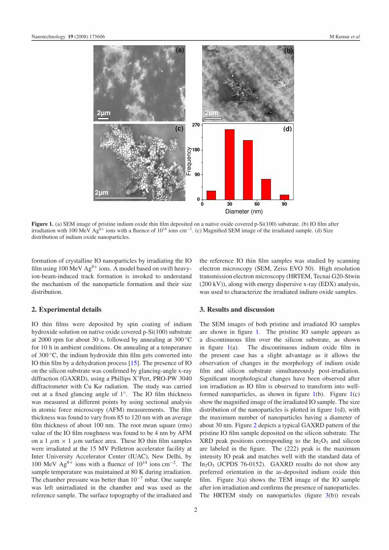
Figure 1. (a) SEM image of pristine indium oxide thin film deposited on a native oxide covered p-Si(100) substrate. (b) IO film afterirradiation with 100 MeV Ag8+ ions with a fluence of 1014 ions cm−2. (c) Magnified SEM image of the irradiated sample. (d) Sizedistribution of indium oxide nanoparticles.
formation of crystalline IO nanoparticles by irradiating the IOfilm using 100 MeV Ag8+ ions. A model based on swift heavy-ion-beam-induced track formation is invoked to understandthe mechanism of the nanoparticle formation and their sizedistribution.
2. Experimental details
IO thin films were deposited by spin coating of indiumhydroxide solution on native oxide covered p-Si(100) substrateat 2000 rpm for about 30 s, followed by annealing at 300 ◦Cfor 10 h in ambient conditions. On annealing at a temperatureof 300 ◦C, the indium hydroxide thin film gets converted intoIO thin film by a dehydration process [15]. The presence of IOon the silicon substrate was confirmed by glancing-angle x-raydiffraction (GAXRD), using a Phillips X’Pert, PRO-PW 3040diffractometer with Cu Kα radiation. The study was carriedout at a fixed glancing angle of 1◦. The IO film thicknesswas measured at different points by using sectional analysisin atomic force microscopy (AFM) measurements. The filmthickness was found to vary from 85 to 120 nm with an averagefilm thickness of about 100 nm. The root mean square (rms)value of the IO film roughness was found to be 4 nm by AFMon a 1 μm × 1 μm surface area. These IO thin film sampleswere irradiated at the 15 MV Pelletron accelerator facility atInter University Accelerator Center (IUAC), New Delhi, by100 MeV Ag8+ ions with a fluence of 1014 ions cm−2. Thesample temperature was maintained at 80 K during irradiation.The chamber pressure was better than 10−7 mbar. One samplewas left unirradiated in the chamber and was used as thereference sample. The surface topography of the irradiated and
the reference IO thin film samples was studied by scanningelectron microscopy (SEM, Zeiss EVO 50). High resolutiontransmission electron microscopy (HRTEM, Tecnai G20-Stwin(200 kV)), along with energy dispersive x-ray (EDX) analysis,was used to characterize the irradiated indium oxide samples.
3. Results and discussion
The SEM images of both pristine and irradiated IO samplesare shown in figure 1. The pristine IO sample appears asa discontinuous film over the silicon substrate, as shownin figure 1(a). The discontinuous indium oxide film inthe present case has a slight advantage as it allows theobservation of changes in the morphology of indium oxidefilm and silicon substrate simultaneously post-irradiation.Significant morphological changes have been observed afterion irradiation as IO film is observed to transform into well-formed nanoparticles, as shown in figure 1(b). Figure 1(c)show the magnified image of the irradiated IO sample. The sizedistribution of the nanoparticles is plotted in figure 1(d), withthe maximum number of nanoparticles having a diameter ofabout 30 nm. Figure 2 depicts a typical GAXRD pattern of thepristine IO film sample deposited on the silicon substrate. TheXRD peak positions corresponding to the In2O3 and siliconare labeled in the figure. The (222) peak is the maximumintensity IO peak and matches well with the standard data ofIn2O3 (JCPDS 76-0152). GAXRD results do not show anypreferred orientation in the as-deposited indium oxide thinfilm. Figure 3(a) shows the TEM image of the IO sampleafter ion irradiation and confirms the presence of nanoparticles.The HRTEM study on nanoparticles (figure 3(b)) reveals
2

Nanotechnology 19 (2008) 175606 M Kumar et al
Figure 2. Glancing-angle XRD pattern of the pristine indium oxidethin film sample deposited on the silicon substrate. The maximumintense peak corresponds to the underlying silicon substrate.
the crystalline nature of the nanoparticles, and the spacingbetween two consecutive lattice planes corresponds to thatof the (220) planes of IO. An EDX-equipped TEM wasused to study the compositional analysis of the indium oxidenanoparticles. Figure 3(c) shows the characteristic x-rayintensity corresponding to different elements versus the energyof the x-ray signal. Standard Tecnai Imaging and Analysis(TIA) software was used to identify the presence of differentelements by matching the observed line positions with itsalready stored data base. The software calculated the atomicpercentage of In and O elements, and confirmed the presenceof IO with In:O atomic ratio of 35:65, which is quite close tothe stoichiometric value of 40:60.
A swift heavy ion (SHI) while traversing through a solidloses its energy in two ways: (1) electronic energy losses(Se) due to inelastic collision of the incoming ion with theelectrons of the solid and (2) nuclear energy losses (Sn) dueto elastic collision with the atoms of the solid [10, 16, 17].These two processes take place in different energy ranges. Thevariation of Se and Sn for 100 MeV Ag8+ ions incident onIO film with the film thickness from the surface is shown infigure 4. These values were calculated through the MonteCarlo based simulation code Stopping and Range of Ions inMatter (SRIM) [18]. Near the surface region, Se exceeds Sn
by two orders of magnitude and is nearly constant throughoutthe film thickness, as shown in the inset of figure 4. Thisindicates that the structural and morphological changes in IOfilm on irradiation by 100 MeV Ag ions are due to electronicexcitations.
There are various models which have been proposed toaccount for the SHI-induced modification in the materials,such as the thermal spike model [19], Coulomb explosionmodel [20, 21], and lattice instability model [22]. Accordingto the thermal spike model, a target material is considered to bemade of electronic and atomic subsystems. The SHI initiallyinteracts with the electronic subsystem and transfers its energyto electrons of the target in a time less than 10−16 s [19].The timescale of electron–ion interaction is very small, andinitially the lattice does not respond in that timescale. Theheat transferred from the electronic subsystem to the atomic
Figure 3. TEM analysis of 100 MeV Ag8+-ion-irradiated indiumoxide sample. (a) The TEM image shows the presence ofnanoparticles. (b) The HRTEM image show the crystalline nature ofthe nanoparticle; the spacing between the two conjugative latticeplanes corresponds to that of the (220) plane of indium oxide.(c) EDX measurement on these nanoparticle samples shows thepresence of indium oxide with In:O ratio of 35:65.
subsystem is substantial only between 10−14 and 10−12 s,depending on the coupling between the two subsystems.The relaxation/transfer of the excess energy of the excitedelectronic subsystem of the target material to the target atomicsubsystem may lead to an increase in the local temperature ofthe material and therefore a high-energy region is created inthe close vicinity (a few nm) of the projectile ion path. ForSe > Seth, the threshold electronic energy loss required for theformation of a latent track, with an efficient electron–phononcoupling, which is defined as the ability of electrons to transfertheir energy to the lattice, a cylindrical region around the trackof the ion may become fluid. The electron–phonon couplingefficiency (g) depends on the ion velocity [23]. In the presentstudy, the value of g is taken to be 0.4 [24]. Therefore, forSe > Seth, MeV ions impinging on the target produce a strongionization of target atoms located along the ion trajectory. For
3

Nanotechnology 19 (2008) 175606 M Kumar et al
Figure 4. Variation of electronic energy loss Se and nuclear energyloss Sn of 100 MeV Ag8+ ions incident on indium oxide film as afunction of film thickness. The inset shows the almost constant valueof Se for even 500 nm depth from the surface of the film.
the present case of 100 MeV Ag8+ ions irradiating the IOfilm, Se is 21.27 keV nm−1 (see figure 4), which is higher thanthe threshold value Seth of 1.23 keV nm−1, calculated later inthe paper. It is also important to note that Se remains almostconstant and dominates over Sn throughout the thickness(∼100 nm) of the IO film. The range of 100 MeV Ag8+ ions inthe IO film is about 9 μm. Thus, Ag8+ ions penetrate deep intothe Si substrate and get implanted there. For Si, the thresholdvalue of track formation Seth is 30 keV nm−1, which is greaterthan the available Se of 21.23 keV nm−1 induced by 100 MeVAg8+ ions [25]. Therefore, latent track formation is onlypossible in the IO film but not in the Si substrate. The valuesof Se and Sn for 100 MeV Ag8+-ion-irradiated IO thin film onSi substrate are listed in the table 1 along with the requiredvalue of Seth. The heat conduction and the temperature of thetarget material are the deciding parameters to determine thediameter of the latent tracks. The rise in the local temperature,T , around the ion trajectory for the present case is calculatedfrom the following equation [26].
Pb = εσ(T 4 − T 4
irr
)(1)
where Pb is the input power density of the beam, ε is theeffective emittance of the IO thin film (assuming ε = 0.2), σ isthe Stephan–Boltzmann constant (5.67 ×10⁻¹² W cm−2 K−4),and Tirr is the substrate temperature (80 K) during irradiation.This gives the value of peak temperature of about 1500 K,which is higher than the melting temperature of 1123 K ofthe IO film [27]. The melting occurs locally in the regionwhere the thermal spike temperature is greater than the meltingtemperature of the material.
Let us now consider that there is a considerable ion-induced local temperature increase �T (r, t) in the material,where r and t are the distance from the ion trajectory andtime, respectively. This can be described by a radial Gaussiandistribution. The ion-induced initial local temperaturedistribution is characterized by the width of the thermal spike,a(0). The target material melts in the region where itstemperature (�T + Tirr) exceeds the melting point Tm of
Table 1. The values of electronic energy loss (Se) and nuclearenergy loss (Sn) for 100 MeV Ag8+-ion-irradiated indium oxide filmdeposited on a native oxide covered silicon substrate determined bySRIM [18]. The threshold value of track formation (Seth) andpossibility of track formation are also mentioned.
Parameters In2O3 Si
Nuclear energy loss(Sn in keV nm−1)
0.13 0.059
Electronic energy loss(Se in keV nm−1)
21.27 10.51
Threshold electrical energyloss (Se in eV nm−1)
1.23 30
Track formation Possible Not possible
IO film. This condition can be expressed as follows:
�T (r, t) + Tirr > Tm. (2)
Therefore, to reach the melting point, the temperature in thethermal spike should increase by T0, where T0 = Tm − Tirr.The radius of the track is defined as [28]
R2e = a2(0) ln(Se/Seth), 1 � Se/Seth � 2.7
= [a2(0)/2.7](Se/Seth), Se/Seth > 2.7. (3)
The value of Seth depends on the material parameters such asdensity ρ, average specific heat c, initial width of the thermalspike a(0), and electron–phonon coupling efficiency g, and canbe determined from the following equation [28]:
Seth = πρca2(0)T0/g. (4)
It is found that, for semiconductors, the value of a(0) dependson their band gap Eg, while for insulators it is almostconstant [16]. The expression a(0) = B + C(Eg)
−1/2, whereB and C are constants, provides a good approximation forthe width of the ion-induced thermal spike in semiconductors.Using an Eg value of 3.7 eV for IO, the value of a(0) was
determined from the plot of E−1/2g versus a(0) as given in [16],
and was found to be 6.2 nm. The value of Seth for IO wascalculated from equation (4) by substituting the values ofmaterial density (ρ = 7.17 gm cm−3), average specific heat(c = 0.0889 J g−1 K−1), melting temperature (Tm = 1123 K),irradiation temperature (Tirr = 80 K) for IO, and was found tobe 1.23 keV nm−1. The track radius Re was calculated fromequation (3) as 15 nm. The complete process of structuraltransformation of IO thin film into nanoparticles by 100 MeVsilver ion irradiation is schematically described in figure 5.It is interesting to note that the calculated value of the trackdiameter matches well with the average size of nanoparticlesobtained from the SEM micrographs.
The mechanism of conversion of ion-induced latent tracksinto nanoparticles is now considered. The 100 MeV Ag8+ions produce latent tracks in IO but not in the Si substrate.Therefore, this discontinuity in the track formation results ina compressive stress at the IO/Si substrate interface. Lianet al have reported ion-beam-induced dewetting of Co thin filmdeposited on native oxide covered silicon substrate [8]. Thesurface energy difference of melted Co and underlying silicon
4
Nanotechnology 19 (2008) 175606 M Kumar et al
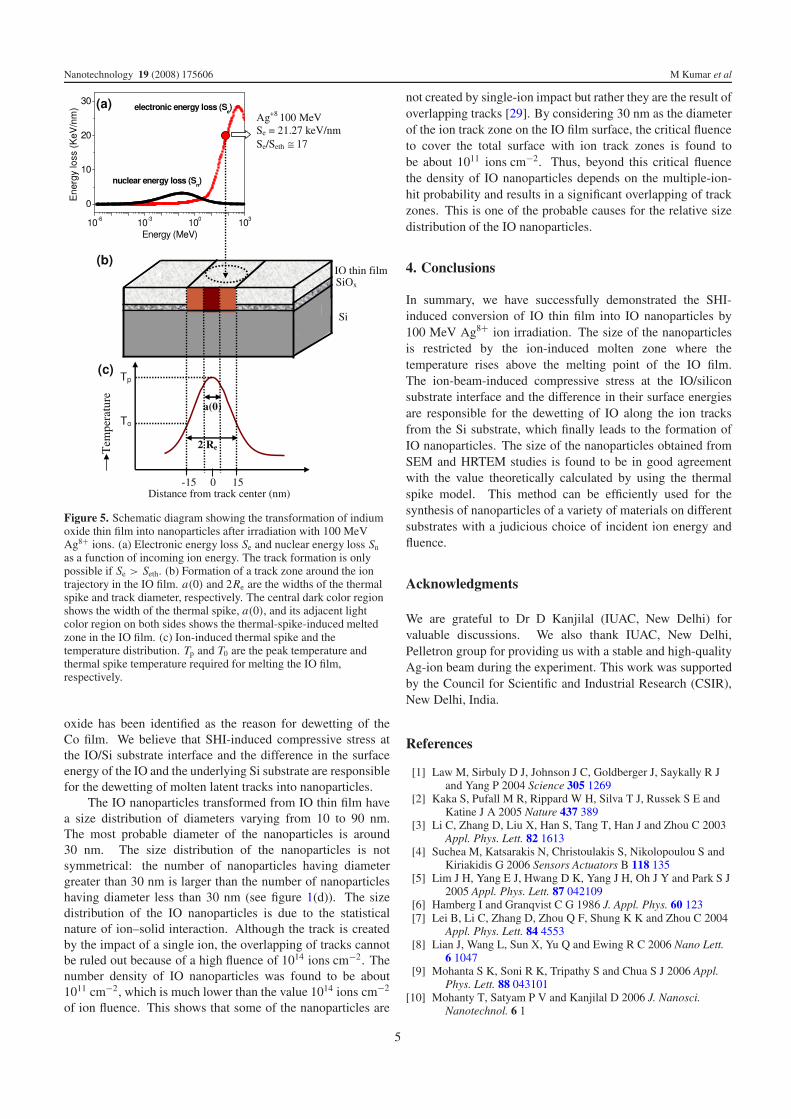
Figure 5. Schematic diagram showing the transformation of indiumoxide thin film into nanoparticles after irradiation with 100 MeVAg8+ ions. (a) Electronic energy loss Se and nuclear energy loss Sn
as a function of incoming ion energy. The track formation is onlypossible if Se > Seth. (b) Formation of a track zone around the iontrajectory in the IO film. a(0) and 2Re are the widths of the thermalspike and track diameter, respectively. The central dark color regionshows the width of the thermal spike, a(0), and its adjacent lightcolor region on both sides shows the thermal-spike-induced meltedzone in the IO film. (c) Ion-induced thermal spike and thetemperature distribution. Tp and T0 are the peak temperature andthermal spike temperature required for melting the IO film,respectively.
oxide has been identified as the reason for dewetting of theCo film. We believe that SHI-induced compressive stress atthe IO/Si substrate interface and the difference in the surfaceenergy of the IO and the underlying Si substrate are responsiblefor the dewetting of molten latent tracks into nanoparticles.
The IO nanoparticles transformed from IO thin film havea size distribution of diameters varying from 10 to 90 nm.The most probable diameter of the nanoparticles is around30 nm. The size distribution of the nanoparticles is notsymmetrical: the number of nanoparticles having diametergreater than 30 nm is larger than the number of nanoparticleshaving diameter less than 30 nm (see figure 1(d)). The sizedistribution of the IO nanoparticles is due to the statisticalnature of ion–solid interaction. Although the track is createdby the impact of a single ion, the overlapping of tracks cannotbe ruled out because of a high fluence of 1014 ions cm−2. Thenumber density of IO nanoparticles was found to be about1011 cm−2, which is much lower than the value 1014 ions cm−2
of ion fluence. This shows that some of the nanoparticles are
not created by single-ion impact but rather they are the result ofoverlapping tracks [29]. By considering 30 nm as the diameterof the ion track zone on the IO film surface, the critical fluenceto cover the total surface with ion track zones is found tobe about 1011 ions cm−2. Thus, beyond this critical fluencethe density of IO nanoparticles depends on the multiple-ion-hit probability and results in a significant overlapping of trackzones. This is one of the probable causes for the relative sizedistribution of the IO nanoparticles.
4. Conclusions
In summary, we have successfully demonstrated the SHI-induced conversion of IO thin film into IO nanoparticles by100 MeV Ag8+ ion irradiation. The size of the nanoparticlesis restricted by the ion-induced molten zone where thetemperature rises above the melting point of the IO film.The ion-beam-induced compressive stress at the IO/siliconsubstrate interface and the difference in their surface energiesare responsible for the dewetting of IO along the ion tracksfrom the Si substrate, which finally leads to the formation ofIO nanoparticles. The size of the nanoparticles obtained fromSEM and HRTEM studies is found to be in good agreementwith the value theoretically calculated by using the thermalspike model. This method can be efficiently used for thesynthesis of nanoparticles of a variety of materials on differentsubstrates with a judicious choice of incident ion energy andfluence.
Acknowledgments
We are grateful to Dr D Kanjilal (IUAC, New Delhi) forvaluable discussions. We also thank IUAC, New Delhi,Pelletron group for providing us with a stable and high-qualityAg-ion beam during the experiment. This work was supportedby the Council for Scientific and Industrial Research (CSIR),New Delhi, India.
References
[1] Law M, Sirbuly D J, Johnson J C, Goldberger J, Saykally R Jand Yang P 2004 Science 305 1269
[2] Kaka S, Pufall M R, Rippard W H, Silva T J, Russek S E andKatine J A 2005 Nature 437 389
[3] Li C, Zhang D, Liu X, Han S, Tang T, Han J and Zhou C 2003Appl. Phys. Lett. 82 1613
[4] Suchea M, Katsarakis N, Christoulakis S, Nikolopoulou S andKiriakidis G 2006 Sensors Actuators B 118 135
[5] Lim J H, Yang E J, Hwang D K, Yang J H, Oh J Y and Park S J2005 Appl. Phys. Lett. 87 042109
[6] Hamberg I and Granqvist C G 1986 J. Appl. Phys. 60 123[7] Lei B, Li C, Zhang D, Zhou Q F, Shung K K and Zhou C 2004
Appl. Phys. Lett. 84 4553[8] Lian J, Wang L, Sun X, Yu Q and Ewing R C 2006 Nano Lett.
6 1047[9] Mohanta S K, Soni R K, Tripathy S and Chua S J 2006 Appl.
Phys. Lett. 88 043101[10] Mohanty T, Satyam P V and Kanjilal D 2006 J. Nanosci.
Nanotechnol. 6 1
5

Nanotechnology 19 (2008) 175606 M Kumar et al
[11] Balamurugan B, Mehta B R, Avasthi D K, Singh F, Arora A K,Rajalakshmi M, Raghavan G, Tyagi A K andShivaprasad S M 2002 J. Appl. Phys. 92 3304
[12] Wang YQ, Smirani R and Ross G G 2004 Nano Lett. 4 2041[13] Tetelbaum D I, Gorshkov O N, Trushun S A, Revin D G,
Gaponova D M and Eckstein W 2000 Nanotechnology11 295
[14] Borsella E et al 2002 Nucl. Instrum. Methods B 191 447[15] Singh V N and Mehta B R 2003 J. Phys. D: Appl. Phys. 42
4226[16] Szenes G, Horvath Z E, Pecz B, Paszti F and Toth L 2002 Phys.
Rev. B 65 045206[17] Ryazanov A I, Volkov A E and Klaumunzer S 1995 Phys. Rev.
B 51 12107[18] Zeigler J F, Biersac J P and Littamark U 1999 Stopping and
Range of Ions in Solids vol 1 (New York: Pergamon)[19] Toulemonde M, Dufour C and Paumier E 1992 Phys. Rev. B
46 14362
[20] Bringa E M and Johnson R E 2002 Phys. Rev. Lett.88 165501
[21] Fleischer R L, Price P B and Walker R M J 1965 J. Appl. Phys.36 3645
[22] Stampfli P 1996 Nucl. Instrum. Methods B 107 138[23] Meftah A, Brisard F, Costantini J M, Hage-Ali M, Stoquert J P,
Studer F and Toulemonde M 1993 Phys. Rev. B 48 920[24] Szenes G, Paszti F, Peter A and Popov A I 2000 Nucl. Instrum.
Methods B 166/167 949[25] Canut B, Bonardi N, Ramos S M M and Della-Negra S 1998
Nucl. Instrum. Methods B 146 296[26] Nakata J 1991 Phys. Rev. B 43 14643[27] Lide D R 2004 CRC Handbook of Chemistry and Physics
85th edn (Boca Raton, FL: CRC Press)[28] Szenes G 1995 Phys. Rev. B 51 8026[29] Singh J P, Singh R, Kanjilal D, Mishra N C and
Ganesan V 2000 J. Appl. Phys. 87 2742
6