Synthesis and characterization of ruthenium dioxide nanostructures
Upload
independentCategory
view
0download
0
Pm
ANa
b
c
e
of
a
ARRAA
KINXMD
1
tmitdisttOipat
2
0d
Materials Science and Engineering A 538 (2012) 89– 97
Contents lists available at SciVerse ScienceDirect
Materials Science and Engineering A
jo ur n al hom epage: www.elsev ier .com/ locate /msea
lasticity of indium nanostructures as revealed by synchrotron X-rayicrodiffraction
rief Suriadi Budimana, Gyuhyon Leeb, Michael J. Burekb,1, Dongchan Jangc, Seung Min J. Hane,obumichi Tamuraf, Martin Kunzf, Julia R. Greerc, Ting Y. Tsuib,∗
Center for Integrated Nanotechnologies, Los Alamos National Laboratory, Los Alamos, NM 87545, USAWaterloo Institute for Nanotechnology, University of Waterloo, 200 University Avenue West, Waterloo, ON N2L 3G1, CanadaDivision of Engineering and Applied Science, California Institute of Technology, 1200 E. California Blvd., Pasadena, CA 91125, USAGraduate School of Energy Environment Water Sustainability, Korea Advanced Institute of Science and Technology, 373-1 Guseong Dong, Yuseong Gu, Daejeon 305-701, Republicf KoreaAdvanced Light Source, Lawrence Berkeley National Laboratory, 1 Cyclotron Road, Berkeley, CA 94720, USA
r t i c l e i n f o
rticle history:eceived 10 August 2011eceived in revised form 9 December 2011ccepted 9 January 2012vailable online 17 January 2012
a b s t r a c t
Indium columnar structures with diameters near 1 �m were deformed by uniaxial compression at strainrates of approximately 0.01 and 0.001 s−1. Defect density evolution in the nanopillars was evaluated byapplying synchrotron Laue X-ray microdiffraction (�SLXRD) on the same specimens before and afterdeformation. Results of the �SLXRD measurements indicate that the dislocation density increases as aresult of mechanical deformation and is a strong function of strain rate. These results suggest that the
eywords:ndiumanopillar-ray microdiffractionicrostructureislocation
rate of defect generation during the compression tests exceeds the rate of defect annihilation, implyingthat plasticity in these indium nanostructures commences via dislocation multiplication rather thannucleation processes. This is in contrast with the behaviors of other materials at the nanoscale, such as,gold, tin, molybdenum, and bismuth. A hypothesis based on the dislocation mean-free-path prior to themultiplication process is proposed to explain this variance.
© 2012 Elsevier B.V. All rights reserved.
. Introduction
With the increased insertion of nanoscale electronic and pho-onic devices into technological applications, understanding the
echanical behavior of small scale structures becomes increasinglymportant to ensure life-time and reliability of these products. Inhe context of mechanical properties, one of the important scientificiscoveries was the emergent size dependence of yield strength
n metals once their dimensions are reduced to the micron andub-micron scales [1–9]. For example, as the dimensions of the fea-ure size in face-centered cubic metal like Au are reduced to lesshan 1 �m, their yield strengths may increase by ∼80 times [10].ne of the possible explanations for this size dependence deeply
n the sub-micron regime is the dislocation starvation effect. The
remise of this theory is that as the dimension of single crystalsre reduced to nanometer scale, mobile dislocations glide alongheir slip planes to the free surfaces relatively unimpeded, and∗ Corresponding author. Tel.: +1 519 888 4567x38404; fax: +1 519 746 4979.E-mail address: [email protected] (T.Y. Tsui).
1 New address: School of Engineering and Applied Sciences, Harvard University,9 Oxford Street, Cambridge, MA 02138, USA.
921-5093/$ – see front matter © 2012 Elsevier B.V. All rights reserved.oi:10.1016/j.msea.2012.01.017
therefore annihilate at the free surface without significant interac-tions with other defects. The result is a net reduction in the mobiledislocation density within the nanostructure during mechanicaldeformation. As the sample is further deformed, the few remain-ing mobile dislocations cannot accommodate the imposed plasticstrain, and therefore new dislocations have to be nucleated, whichrequires high stresses. As the nanostructures get smaller, thenumber of available dislocation sources decreases, and their oper-ation strength increases, which leads to the ever higher stressesin smaller samples [1,3,9]. This notion of dislocation starvation,coined by the authors as “mechanical annealing”, has also beendemonstrated via in situ compression of single crystalline nickelpillars [6]. Shan et al. [6] used an in situ transmission electronmicroscope (TEM) nanoindenter to illustrate this size effect andshowed that the initial dislocations in a focused ion beam (FIB)-fabricated 160 nm diameter nickel pillar completely disappearupon mechanical deformation. Budiman et al. [11] used a non-destructive synchrotron Laue X-ray microdiffraction technique toperform ex situ characterization of the defect density within gold
nanopillars before and after the compression tests. These �SLXRDresults showed no detectable increase of the Laue spot diffrac-tion peak broadening, which indicates there is no net increase ofdefect density in the small-scale structures after the mechanical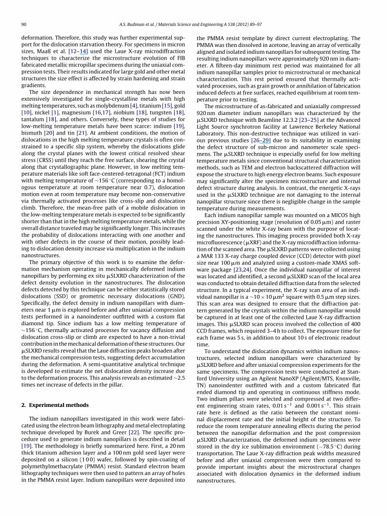
9 ce an
dpstfpsg
em[tlbdsasapwomvctsotwin
mndddSetd∼dc�tditt
2
ctc[tdpli
0 A.S. Budiman et al. / Materials Scien
eformation. Therefore, this study was further experimental sup-ort for the dislocation starvation theory. For specimens in micronizes, Maaß et al. [12–14] used the Laue X-ray microdiffractionechniques to characterize the microstructure evolution of FIBabricated metallic micropillar specimens during the uniaxial com-ression tests. Their results indicated for large gold and other metaltructures the size effect is affected by strain hardening and strainradients.
The size dependence in mechanical strength has now beenxtensively investigated for single-crystalline metals with highelting temperatures, such as molybdenum [4], titanium [15], gold
10], nickel [1], magnesium [16,17], niobium [18], tungsten [18],antalum [18], and others. Conversely, these types of studies forow-melting temperature metals have been scarce: indium [19],ismuth [20] and tin [21]. At ambient conditions, the motion ofislocations in the high melting temperature crystals is often con-trained to a specific slip system, whereby the dislocations glidelong the crystal planes with the lowest critical resolved sheartress (CRSS) until they reach the free surface, shearing the crystallong that crystallographic plane. However, in low melting tem-erature materials like soft face-centered-tetragonal (FCT) indiumith melting temperature of ∼156 ◦C (corresponding to a homol-
gous temperature at room temperature near 0.7), dislocationotion even at room temperature may become non-conservative
ia thermally activated processes like cross-slip and dislocationlimb. Therefore, the mean-free path of a mobile dislocation inhe low-melting temperature metals is expected to be significantlyhorter than that in the high melting temperature metals, while theverall distance traveled may be significantly longer. This increaseshe probability of dislocations interacting with one another andith other defects in the course of their motion, possibly lead-
ng to dislocation density increase via multiplication in the indiumanostructures.
The primary objective of this work is to examine the defor-ation mechanism operating in mechanically deformed indium
anopillars by performing ex situ �SLXRD characterization of theefect density evolution in the nanostructures. The dislocationefects detected by this technique can be either statistically storedislocations (SSD) or geometric necessary dislocations (GND).pecifically, the defect density in indium nanopillars with diam-ters near 1 �m is explored before and after uniaxial compressionests performed in a nanoindenter outfitted with a custom flatiamond tip. Since indium has a low melting temperature of156 ◦C, thermally activated processes for vacancy diffusion andislocation cross-slip or climb are expected to have a non-trivialontribution in the mechanical deformation of these structures. OurSLXRD results reveal that the Laue diffraction peaks broaden after
he mechanical compression tests, suggesting defect accumulationuring the deformation. A semi-quantitative analytical technique
s developed to estimate the net dislocation density increase dueo the deformation process. This analysis reveals an estimated ∼2.5imes net increase of defects in the pillar.
. Experimental methods
The indium nanopillars investigated in this work were fabri-ated using the electron beam lithography and metal electroplatingechnique developed by Burek and Greer [22]. The specific pro-edure used to generate indium nanopillars is described in detail19]. The methodology is briefly summarized here. First, a 20 nmhick titanium adhesion layer and a 100 nm gold seed layer were
eposited on a silicon (1 0 0) wafer, followed by spin-coating ofolymethylmethacrylate (PMMA) resist. Standard electron beamithography techniques were then used to pattern an array of holesn the PMMA resist layer. Indium nanopillars were deposited into
d Engineering A 538 (2012) 89– 97
the PMMA resist template by direct current electroplating. ThePMMA was then dissolved in acetone, leaving an array of verticallyaligned and isolated indium nanopillars for subsequent testing. Theresulting indium nanopillars were approximately 920 nm in diam-eter. A fifteen-day minimum rest period was maintained for allindium nanopillar samples prior to microstructural or mechanicalcharacterization. This rest period ensured that thermally acti-vated processes, such as grain growth or annihilation of fabricationinduced defects at free surfaces, reached equilibrium at room tem-perature prior to testing.
The microstructure of as-fabricated and uniaxially compressed920 nm diameter indium nanopillars was characterized by the�SLXRD technique with Beamline 12.3.2 [23–25] at the AdvancedLight Source synchrotron facility at Lawrence Berkeley NationalLaboratory. This non-destructive technique was utilized in vari-ous previous studies [26–29] due to its suitability in examiningthe defect structure of sub-micron and nanometer scale speci-mens. The �SLXRD technique is especially useful for low meltingtemperature metals since conventional structural characterizationmethods, such as TEM and electron backscattered diffraction willexpose the structure to high energy electron beams. Such exposuremay significantly alter the specimen microstructure and internaldefect structure during analysis. In contrast, the energetic X-raysused in the �SLXRD technique are not damaging to the internalnanopillar structure since there is negligible change in the sampletemperature during measurements.
Each indium nanopillar sample was mounted on a MICOS highprecision XY-positioning stage (resolution of 0.05 �m) and rasterscanned under the white X-ray beam with the purpose of locat-ing the nanostructures. This imaging process provided both X-raymicrofluorescence (�XRF) and the X-ray microdiffraction informa-tion of the scanned area. The �SLXRD patterns were collected usinga MAR 133 X-ray charge coupled device (CCD) detector with pixelsize near 100 �m and analyzed using a custom-made XMAS soft-ware package [23,24]. Once the individual nanopillar of interestwas located and identified, a second �SLXRD scan of the local areawas conducted to obtain detailed diffraction data from the selectedstructure. In a typical experiment, the X-ray scan area of an indi-vidual nanopillar is a ∼10 × 10 �m2 square with 0.5 �m step sizes.This scan area was designed to ensure that the diffraction pat-tern generated by the crystals within the indium nanopillar wouldbe captured in at least one of the collected Laue X-ray diffractionimages. This �SLXRD scan process involved the collection of 400CCD frames, which required 3–4 h to collect. The exposure time foreach frame was 5 s, in addition to about 10 s of electronic readouttime.
To understand the dislocation dynamics within indium nanos-tructures, selected indium nanopillars were characterized by�SLXRD before and after uniaxial compression experiments for thesame specimens. The compression tests were conducted at Stan-ford University using an Agilent NanoXP (Agilent/MTS, Knoxville,TN) nanoindenter outfitted with and a custom fabricated flatended diamond tip and operating in continuous stiffness mode.Two indium pillars were selected and compressed at two differ-ent engineering strain rates, 0.01 s−1 and 0.001 s−1. This strainrate here is defined as the ratio between the constant nomi-nal displacement rate and the initial height of the structure. Toreduce the room temperature annealing effects during the periodbetween the nanopillar deformation and the post compression�SLXRD characterization, the deformed indium specimens werestored in the dry ice sublimation environment (−78.5 ◦C) duringtransportation. The Laue X-ray diffraction peak widths measuredbefore and after uniaxial compression were then compared toprovide important insights about the microstructural changes
associated with dislocation dynamics in the deformed indiumnanostructures.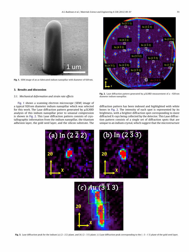
A.S. Budiman et al. / Materials Science and Engineering A 538 (2012) 89– 97 91
F
3
3
afaita
ig. 1. SEM image of an as-fabricated indium nanopillar with diameter of 920 nm.
. Results and discussion
.1. Mechanical deformation and strain rate effects
Fig. 1 shows a scanning electron microscope (SEM) image of typical 920 nm diameter indium nanopillar which was selectedor this work. The Laue diffraction pattern generated by �SLXRDnalysis of this indium nanopillar prior to uniaxial compression
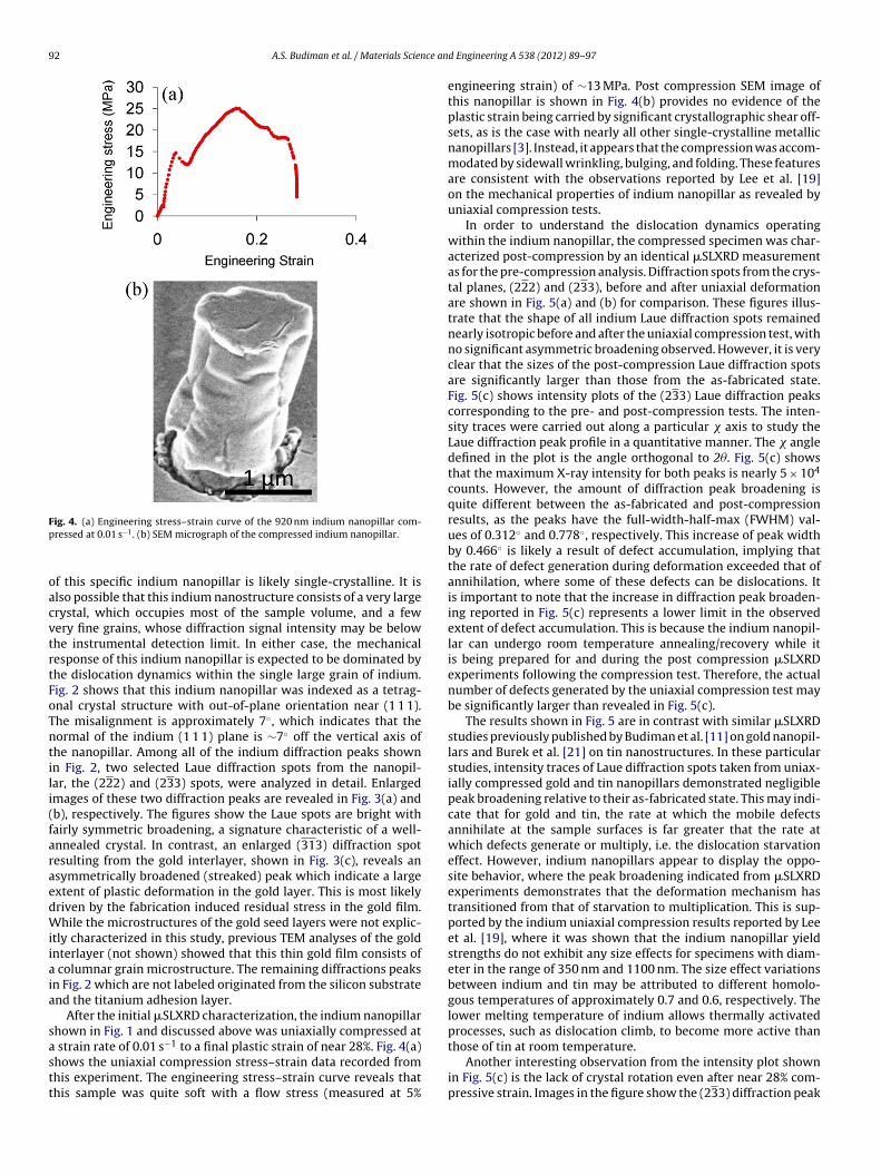
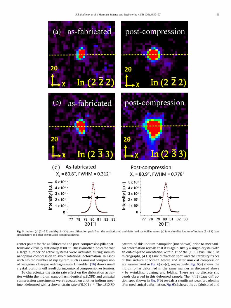
s shown in Fig. 2. This Laue diffraction pattern consists of crys-allographic information from the indium nanopillar, the titaniumdhesion layer, the gold seed layer, and the silicon substrate. TheFig. 3. Laue diffraction peak for the indium (a) (2 −2 2) plane, and (b) (2 −3 3) plane. (c)
Fig. 2. Laue diffraction pattern generated by �SLXRD measurement of a ∼920 nmdiameter indium nanopillar.
diffraction pattern has been indexed and highlighted with whiteboxes in Fig. 2. The intensity of each spot is represented by itsbrightness, with a brighter diffraction spot corresponding to more
diffracted X-rays being collected by the detector. This Laue diffrac-tion pattern consists of a single set of diffraction spots that areunique to an indium crystal, which suggest that the microstructureLaue diffraction peak corresponding to the (−3 −1 3) plane of the gold seed layer.
92 A.S. Budiman et al. / Materials Science an
Fp
oacvtrtFoTntili(faraedWiiaia
sastt
those of tin at room temperature.
ig. 4. (a) Engineering stress–strain curve of the 920 nm indium nanopillar com-ressed at 0.01 s−1. (b) SEM micrograph of the compressed indium nanopillar.
f this specific indium nanopillar is likely single-crystalline. It islso possible that this indium nanostructure consists of a very largerystal, which occupies most of the sample volume, and a fewery fine grains, whose diffraction signal intensity may be belowhe instrumental detection limit. In either case, the mechanicalesponse of this indium nanopillar is expected to be dominated byhe dislocation dynamics within the single large grain of indium.ig. 2 shows that this indium nanopillar was indexed as a tetrag-nal crystal structure with out-of-plane orientation near (1 1 1).he misalignment is approximately 7◦, which indicates that theormal of the indium (1 1 1) plane is ∼7◦ off the vertical axis ofhe nanopillar. Among all of the indium diffraction peaks shownn Fig. 2, two selected Laue diffraction spots from the nanopil-ar, the (222) and (233) spots, were analyzed in detail. Enlargedmages of these two diffraction peaks are revealed in Fig. 3(a) andb), respectively. The figures show the Laue spots are bright withairly symmetric broadening, a signature characteristic of a well-nnealed crystal. In contrast, an enlarged (313) diffraction spotesulting from the gold interlayer, shown in Fig. 3(c), reveals ansymmetrically broadened (streaked) peak which indicate a largextent of plastic deformation in the gold layer. This is most likelyriven by the fabrication induced residual stress in the gold film.hile the microstructures of the gold seed layers were not explic-
tly characterized in this study, previous TEM analyses of the goldnterlayer (not shown) showed that this thin gold film consists of
columnar grain microstructure. The remaining diffractions peaksn Fig. 2 which are not labeled originated from the silicon substratend the titanium adhesion layer.
After the initial �SLXRD characterization, the indium nanopillarhown in Fig. 1 and discussed above was uniaxially compressed at
strain rate of 0.01 s−1 to a final plastic strain of near 28%. Fig. 4(a)
hows the uniaxial compression stress–strain data recorded fromhis experiment. The engineering stress–strain curve reveals thathis sample was quite soft with a flow stress (measured at 5%d Engineering A 538 (2012) 89– 97
engineering strain) of ∼13 MPa. Post compression SEM image ofthis nanopillar is shown in Fig. 4(b) provides no evidence of theplastic strain being carried by significant crystallographic shear off-sets, as is the case with nearly all other single-crystalline metallicnanopillars [3]. Instead, it appears that the compression was accom-modated by sidewall wrinkling, bulging, and folding. These featuresare consistent with the observations reported by Lee et al. [19]on the mechanical properties of indium nanopillar as revealed byuniaxial compression tests.
In order to understand the dislocation dynamics operatingwithin the indium nanopillar, the compressed specimen was char-acterized post-compression by an identical �SLXRD measurementas for the pre-compression analysis. Diffraction spots from the crys-tal planes, (222) and (233), before and after uniaxial deformationare shown in Fig. 5(a) and (b) for comparison. These figures illus-trate that the shape of all indium Laue diffraction spots remainednearly isotropic before and after the uniaxial compression test, withno significant asymmetric broadening observed. However, it is veryclear that the sizes of the post-compression Laue diffraction spotsare significantly larger than those from the as-fabricated state.Fig. 5(c) shows intensity plots of the (233) Laue diffraction peakscorresponding to the pre- and post-compression tests. The inten-sity traces were carried out along a particular � axis to study theLaue diffraction peak profile in a quantitative manner. The � angledefined in the plot is the angle orthogonal to 2�. Fig. 5(c) showsthat the maximum X-ray intensity for both peaks is nearly 5 × 10⁴
counts. However, the amount of diffraction peak broadening isquite different between the as-fabricated and post-compressionresults, as the peaks have the full-width-half-max (FWHM) val-ues of 0.312◦ and 0.778◦, respectively. This increase of peak widthby 0.466◦ is likely a result of defect accumulation, implying thatthe rate of defect generation during deformation exceeded that ofannihilation, where some of these defects can be dislocations. Itis important to note that the increase in diffraction peak broaden-ing reported in Fig. 5(c) represents a lower limit in the observedextent of defect accumulation. This is because the indium nanopil-lar can undergo room temperature annealing/recovery while itis being prepared for and during the post compression �SLXRDexperiments following the compression test. Therefore, the actualnumber of defects generated by the uniaxial compression test maybe significantly larger than revealed in Fig. 5(c).
The results shown in Fig. 5 are in contrast with similar �SLXRDstudies previously published by Budiman et al. [11] on gold nanopil-lars and Burek et al. [21] on tin nanostructures. In these particularstudies, intensity traces of Laue diffraction spots taken from uniax-ially compressed gold and tin nanopillars demonstrated negligiblepeak broadening relative to their as-fabricated state. This may indi-cate that for gold and tin, the rate at which the mobile defectsannihilate at the sample surfaces is far greater that the rate atwhich defects generate or multiply, i.e. the dislocation starvationeffect. However, indium nanopillars appear to display the oppo-site behavior, where the peak broadening indicated from �SLXRDexperiments demonstrates that the deformation mechanism hastransitioned from that of starvation to multiplication. This is sup-ported by the indium uniaxial compression results reported by Leeet al. [19], where it was shown that the indium nanopillar yieldstrengths do not exhibit any size effects for specimens with diam-eter in the range of 350 nm and 1100 nm. The size effect variationsbetween indium and tin may be attributed to different homolo-gous temperatures of approximately 0.7 and 0.6, respectively. Thelower melting temperature of indium allows thermally activatedprocesses, such as dislocation climb, to become more active than
Another interesting observation from the intensity plot shownin Fig. 5(c) is the lack of crystal rotation even after near 28% com-pressive strain. Images in the figure show the (233) diffraction peak
A.S. Budiman et al. / Materials Science and Engineering A 538 (2012) 89– 97 93
F cated
s
ctanwoc
tci
ig. 5. Indium (a) (2 −2 2) and (b) (2 −3 3) Laue diffraction peak from the as-fabripeak before and after the uniaxial compression test.
enter points for the as-fabricated and post-compression pillar pat-erns are virtually stationary at 80.8◦. This is another indicator that
large number of active systems were available during indiumanopillar compression to avoid rotational deformation. In casesith limited number of slip system, such as uniaxial compression
f hexagonal close packed magnesium, Lilleodden [16] shows smallrystal rotations will result during uniaxial compression or tension.
To characterize the strain rate effect on the dislocation activi-ies within the indium nanopillars, identical �SLXRD and uniaxialompression experiments were repeated on another indium spec-men deformed with a slower strain rate of 0.001 s−1. The �SLXRD
and deformed nanopillar states. (c) Intensity distribution of indium (2 −3 3) Laue
pattern of this indium nanopillar (not shown) prior to mechani-cal deformation reveals that it is again, likely a single-crystal withan out-of-plane orientation within 1◦ of the (1 1 0) axis. The SEMmicrographs, (4 1 3) Laue diffraction spot, and the intensity tracesof this indium specimen before and after uniaxial compressionare summarized in Fig. 6(a)–(c), respectively. Fig. 6(a) shows theindium pillar deformed in the same manner as discussed above
– by wrinkling, bulging, and folding. There are no discrete slipbands observed in this deformed sample. The (4 1 3) Laue diffrac-tion spot shown in Fig. 6(b) reveals a significant peak broadeningafter mechanical deformation. Fig. 6(c) shows the as-fabricated and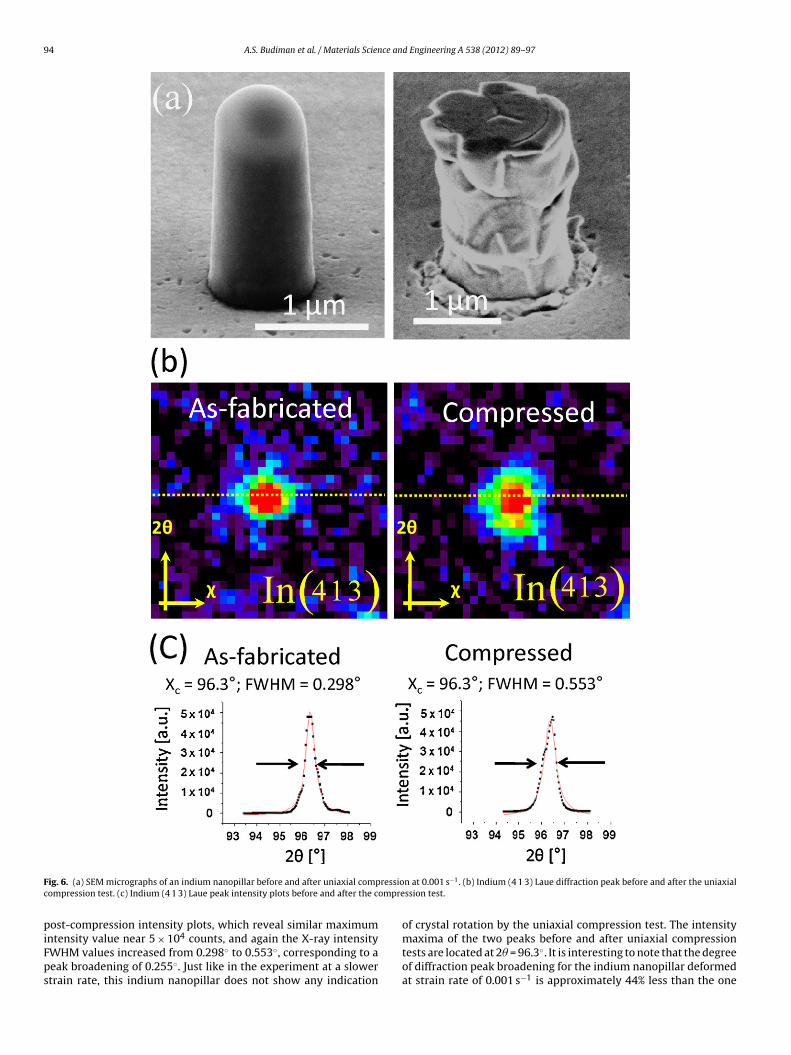
94 A.S. Budiman et al. / Materials Science and Engineering A 538 (2012) 89– 97
F ressioc ompre
piFps
ig. 6. (a) SEM micrographs of an indium nanopillar before and after uniaxial compompression test. (c) Indium (4 1 3) Laue peak intensity plots before and after the c
ost-compression intensity plots, which reveal similar maximum
ntensity value near 5 × 10⁴ counts, and again the X-ray intensityWHM values increased from 0.298◦ to 0.553◦, corresponding to aeak broadening of 0.255◦. Just like in the experiment at a slowertrain rate, this indium nanopillar does not show any indicationn at 0.001 s−1. (b) Indium (4 1 3) Laue diffraction peak before and after the uniaxialssion test.
of crystal rotation by the uniaxial compression test. The intensity
maxima of the two peaks before and after uniaxial compressiontests are located at 2� = 96.3◦. It is interesting to note that the degreeof diffraction peak broadening for the indium nanopillar deformedat strain rate of 0.001 s−1 is approximately 44% less than the one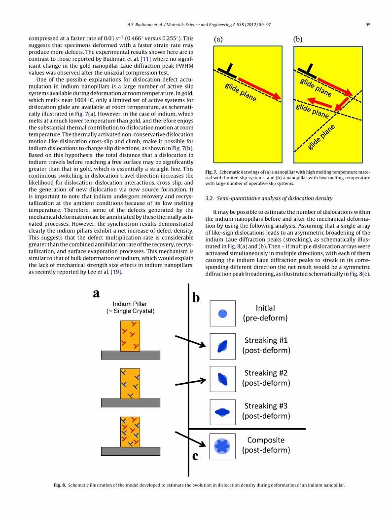
ce and Engineering A 538 (2012) 89– 97 95
cspciv
mswdcmttmiBigcltittmvcTgtsta
A.S. Budiman et al. / Materials Scien
ompressed at a faster rate of 0.01 s−1 (0.466◦ versus 0.255◦). Thisuggests that specimens deformed with a faster strain rate mayroduce more defects. The experimental results shown here are inontrast to those reported by Budiman et al. [11] where no signif-cant change in the gold nanopillar Laue diffraction peak FWHMalues was observed after the uniaxial compression test.
One of the possible explanations for dislocation defect accu-ulation in indium nanopillars is a large number of active slip
ystems available during deformation at room temperature. In gold,hich melts near 1064 ◦C, only a limited set of active systems forislocation glide are available at room temperature, as schemati-ally illustrated in Fig. 7(a). However, in the case of indium, whichelts at a much lower temperature than gold, and therefore enjoys
he substantial thermal contribution to dislocation motion at roomemperature. The thermally activated non-conservative dislocation
otion like dislocation cross-slip and climb, make it possible forndium dislocations to change slip directions, as shown in Fig. 7(b).ased on this hypothesis, the total distance that a dislocation in
ndium travels before reaching a free surface may be significantlyreater than that in gold, which is essentially a straight line. Thisontinuous switching in dislocation travel direction increases theikelihood for dislocation–dislocation interactions, cross-slip, andhe generation of new dislocation via new source formation. Its important to note that indium undergoes recovery and recrys-allization at the ambient conditions because of its low meltingemperature. Therefore, some of the defects generated by the
echanical deformation can be annihilated by these thermally acti-ated processes. However, the synchrotron results demonstratedlearly the indium pillars exhibit a net increase of defect density.his suggests that the defect multiplication rate is considerablereater than the combined annihilation rate of the recovery, recrys-
allization, and surface evaporation processes. This mechanism isimilar to that of bulk deformation of indium, which would explainhe lack of mechanical strength size effects in indium nanopillars,s recently reported by Lee et al. [19].Fig. 8. Schematic illustration of the model developed to estimate the evoluti
Fig. 7. Schematic drawings of (a) a nanopillar with high melting temperature mate-rial with limited slip systems, and (b) a nanopillar with low melting temperaturewith large number of operative slip systems.
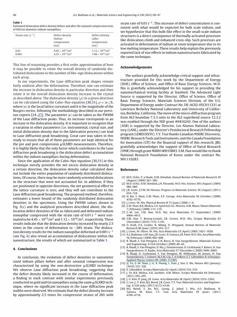
3.2. Semi-quantitative analysis of dislocation density
It may be possible to estimate the number of dislocations withinthe indium nanopillars before and after the mechanical deforma-tion by using the following analysis. Assuming that a single arrayof like-sign dislocations leads to an asymmetric broadening of theindium Laue diffraction peaks (streaking), as schematically illus-trated in Fig. 8(a) and (b). Then – if multiple dislocation arrays were
activated simultaneously in multiple directions, with each of themcausing the indium Laue diffraction peaks to streak in its corre-sponding different direction the net result would be a symmetricdiffraction peak broadening, as illustrated schematically in Fig. 8(c).on in dislocation density during deformation of an indium nanopillar.
96 A.S. Budiman et al. / Materials Science an
Table 1Estimated dislocation defect density before and after the uniaxial compression testsof 920 nm diameter indium nanopillars.
Strain rate (s−1) Defect density(beforecompressiontest)
Defect density(aftercompressiontest)
Tite
ftracwBooiaitstidw
tantiatLedFlnmrtt(n
4
scWtacnwb
[[
[
[
[
[
[[
[
0.01 4.45 × 10¹³/m2 1.12 × 10¹⁴/m2
0.001 4.25 × 10¹³/m2 7.88 × 10¹³/m2
his line of reasoning provides a first order approximation of howt may be possible to relate the overall density of randomly dis-ributed dislocations to the number of like-sign dislocations withinach array.
In our experiments, the Laue diffraction peak shapes remainairly uniform after the deformation. Therefore, one can estimatehe increase in dislocation density in particular direction and thenelate it to the overall dislocation density increase in the crystals described above. The dislocation density (�) in a given directionan be calculated using the Cahn–Nye equation [30,31], � = |�| /b,here |�| is the local lattice curvature and b is the magnitude of theurgers vector, following the methodology described in our previ-us reports [24–27]. The parameter |�| can be taken as the FWHMf the Laue diffraction peaks. Thus, its increase corresponds to anncrease in the dislocation density. It is important to recognize that
variation in other parameters (i.e. instrumental, crystal size, andnitial dislocation density due to the fabrication process) can leado Laue diffraction peak broadening. Great care was taken in thistudy to ensure that all of these parameters are kept identical forhe pre and post compression �SLXRD measurements. Therefore,t is highly likely that the only factor which contributes to the Laueiffraction peak broadening is the dislocation defect accumulationithin the indium nanopillars during deformation.
Since the application of the Cahn–Nye equation [30,31] in thisechnique merely provides the net excess dislocation density in
certain direction, the dislocation density value calculated doesot include the entire population of randomly distributed disloca-ions. Of course, there may be more randomly oriented dislocationsn the structure that were not accounted for. In addition, if theyre positioned in opposite directions, the net geometrical effect tohe lattice curvature is zero, and they will not contribute to theaue diffraction peak broadening. The proposed method, therefore,stimates a lower bound of the randomly distributed dislocationensities in the specimens. Using the FWHM values shown inig. 5(c) and the analytical procedures described above, the dis-ocation defect densities of the as-fabricated and deformed indiumanopillar compressed with the strain rate of 0.01 s−1 were esti-ated to be 4.45 × 10¹³/m2 and 1.12 × 10¹⁴/m2, respectively. These
esults indicate that the dislocation density increased by nearly 2.5imes in the course of deformation to ∼28% strain. The disloca-ion density results for the indium nanopillar deformed at 0.001 s−1
see Fig. 6) also reveal an accumulation of dislocations within theanostructure, the results of which are summarized in Table 1.
. Conclusions
In conclusion, the evolution of defect densities in nanometerized indium pillars before and after uniaxial compression washaracterized by using the non-destructive �SLXRD technique.
e observe Laue diffraction peak broadening, suggesting thathe defect density likely increased in the course of deformation,
finding in stark contrast with similar experiments previously
onducted on gold and tin nanopillars using the same �SLXRD tech-ique, where no significant increase in the Laue diffraction peakidths were observed. We estimate that the defect density increasey approximately 2.5 times for compressive strains of 28% with
[
[
d Engineering A 538 (2012) 89– 97
strain rate of 0.01 s−1. This increase of defect concentration is con-sistent with what would be expected for bulk scale indium, andwe hypothesize that this bulk-like effect in the small-scale indiumstructures is a direct consequence of thermally activated processeslike dislocation climb and enhanced cross-slip. Such processes areactivated in deformation of indium at room temperature due to itslow melting temperature. These results help explain the previouslyreported lack of size effects in indium nanostructures fabricated bythe same technique.
Acknowledgements
The authors gratefully acknowledge critical support and infras-tructure provided for this work by the Department of Energy(DOE), Office of Science, and Office of Basic Energy Sciences. W.D.Nix is gratefully acknowledged for his support in providing thenanomechanical testing facility at Stanford. The Advanced LightSource is supported by the Director, Office of Science, Office ofBasic Energy Sciences, Materials Sciences Division, of the U.S.Department of Energy under Contract No. DE-AC02-05CH11231 atLawrence Berkeley National Laboratory and University of Califor-nia, Berkeley, California. The move of the micro-diffraction programfrom ALS beamline 7.3.3 onto to the ALS superbend source 12.3.2was enabled through the NSF grant #0416243. One of the authors(ASB) is supported by the Director, Los Alamos National Labora-tory (LANL), under the Director’s Postdoctoral Research Fellowshipprogram (LDRD/X93V). T.Y. Tsui thanks Canadian NSERC Discovery,NSERC Research Tools and Instruments, and the Canada Foundationfor Innovation (CFI) for the financial support of this research. JRGgratefully acknowledges the support of Office of Naval Research(ONR) through grant N000140910883. S.M. Han would like to thankNational Research Foundation of Korea under the contract No.N01110283.
References
[1] M.D. Uchic, P. a Shade, D.M. Dimiduk, Annual Review of Materials Research 39(August) (2009) 361–386.
[2] M.D. Uchic, D.M. Dimiduk, J.N. Florando, W.D. Nix, Science 305 (August) (2004)986–989.
[3] J.R. Greer, J.T.M. De Hosson, Progress in Materials Science 56 (August) (2011)654–724.
[4] H. Bei, S. Shim, G.M. Pharr, E.P. George, Acta Materialia 56 (October) (2008)4762–4770.
[5] J. Greer, W. Nix, Physical Review B 73 (June) (2006) 1–6.[6] Z.W. Shan, R.K. Mishra, S.A. Syed Asif, O.L. Warren, A.M. Minor, Nature Materials
7 (February) (2008) 115–119.[7] S.-W. Lee, S.M. Han, W.D. Nix, Acta Materialia 57 (September) (2009)
4404–4415.[8] S.M. Han, T. Bozorg-Grayeli, J.R. Groves, W.D. Nix, Scripta Materialia 63
(December) (2010) 1153–1156.[9] O. Kraft, P.A. Gruber, R. Mönig, D. Weygand, Annual Review of Materials
Research 40 (June) (2010) 293–317.10] J. Greer, W. Oliver, W. Nix, Acta Materialia 53 (April) (2005) 1821–1830.11] A.S. Budiman, S.M. Han, J.R. Greer, N. Tamura, J.R. Patel, W.D. Nix, Acta Materialia
56 (February) (2008) 602–608.12] R. Maaß, S. Van Petegem, C.N. Borca, H. Van Swygenhoven, Materials Science
and Engineering: A 524 (October) (2009) 40–45.13] R. Maaß, S. Van Petegem, D. Ma, J. Zimmermann, D. Grolimund, F. Roters, H. Van
Swygenhoven, D. Raabe, Acta Materialia 57 (December) (2009) 5996–6005.14] R. Maa�, D. Grolimund, S. Van Petegem, M. Willimann, M. Jensen, H. Van
Swygenhoven, T. Lehnert, M.A.M. Gijs, C.A Volkert, E.T. Lilleodden, R. Schwaiger,Applied Physics Letters 89 (2006) 151905.
15] Q. Yu, Z.-W. Shan, J. Li, X. Huang, L. Xiao, J. Sun, E. Ma, Nature 463 (January)(2010) 335–338.
16] E. Lilleodden, Scripta Materialia 62 (April) (2010) 532–535.17] J. Ye, R.K. Mishra, A.K. Sachdev, A.M. Minor, Scripta Materialia 64 (February)
(2011) 292–295.18] J.-Y. Kim, D. Jang, J.R. Greer, Acta Materialia 58 (April) (2010) 2355–2363.
19] G. Lee, J.-Y. Kim, M.J. Burek, J.R. Greer, T.Y. Tsui, Materials Science and Engineer-ing: A 528 (July) (2011) 6112–6120.20] M.J. Burek, S. Jin, M.C. Leung, Z. Jahed, J. Wu, A.S. Budiman, N.
Tamura, M. Kunz, T.Y. Tsui, Acta Materialia 59 (June) (2011)4709–4718.

ce an
[
[[
[
[
[
[
[
[Misra, Plasticity in the nanoscale Cu/Nb single-crystal multilayers as revealedby synchrotron Laue X-ray microdiffraction, J. Mater. Res., Available on CJO
A.S. Budiman et al. / Materials Scien
21] M.J. Burek, A.S. Budiman, Z. Jahed, N. Tamura, M. Kunz, S. Jin, S.M.J. Han, G. Lee,C. Zamecnik, T.Y. Tsui, Materials Science and Engineering: A 528 (July) (2011)5822–5832.
22] M.J. Burek, J.R. Greer, Nano Letters 10 (2010) 69.23] N. Tamura, R.S. Celestre, A.A. MacDowell, H.A. Padmore, R. Spolenak, B.C. Valek,
N. Meier Chang, A. Manceau, J.R. Patel, Review of Scientific Instruments 73(2002) 1369.
24] N. Tamura, A.A. MacDowell, R. Spolenak, B.C. Valek, J.C. Bravman, W.L. Brown,R.S. Celestre, H.A. Padmore, B.W. Batterman, J.R. Patel, Journal of Synchrotron
Radiation 10 (February) (2003) 137–143.25] M. Kunz, N. Tamura, K. Chen, A.A. MacDowell, R.S. Celestre, M.M. Church, S.Fakra, E.E. Domning, J.M. Glossinger, J.L. Kirschman, G.Y. Morrison, D.W. Plate,B.V. Smith, T. Warwick, V.V. Yashchuk, H.A. Padmore, E. Ustundag, The Reviewof Scientific Instruments 80 (March) (2009) 035108.
[[
d Engineering A 538 (2012) 89– 97 97
26] G. Feng, A.S. Budiman, W.D. Nix, N. Tamura, J.R. Patel, Journal of Applied Physics104 (2008) 043501.
27] A.S. Budiman, W.D. Nix, N. Tamura, B.C. Valek, K. Gadre, J. Maiz, R. Spolenak,J.R. Patel, Applied Physics Letters 88 (2006) 233515.
28] A.S. Budiman, P. Besser, C.S. Hau-Riege, A. Marathe, Y.C. Joo, N. Tamura, J.R.Patel, W.D. Nix, Journal of Electronic Materials 38 (2009) 379–391.
29] A.S. Budiman, S.-M. Han, N. Li, Q.-M. Wei, P. Dickerson, N. Tamura, M. Kunz, A.
doi:10.1557/jmr.2011.421.30] R.W. Cahn, Journal Institute of Metals 76 (1949) 121–141.31] J.F. Nye, Acta Metallurgica 1 (1953) 153–162.
Copyright © 2022 FDOKUMEN