Anomalously Large Pockels Effect in ZnO-F Single Crystalline Films Deposited on Bare Glass
Upload
independentCategory
view
4download
0
Chinese Materials Research Society
Progress in Natural Science: Materials International
Progress in Natural Science: Materials International 2013;23(1):64–69
1002-0071 & 2013 Ch
http://dx.doi.org/10.1
nCorresponding au
fax: þ92 51 2208051
E-mail address:
Peer review unde
Society.
www.elsevier.com/locate/pnsmiwww.sciencedirect.com
ORIGINAL RESEARCH
Structural and optical properties of Cr doped ZnO
crystalline thin films deposited by reactive electron
beam evaporation technique
Amjid Iqbala,n, Arshad Mahmood
a, Taj Muhammad Khan
a, Ejaz Ahmed
b
aNational Institute of Laser and Optronics (NILOP), P.O. Nilore, Islamabad 45650, PakistanbPhysics Division PINSTECH, P.O. Nilore, Islamabad 45650, Pakistan
Received 28 July 2012; accepted 27 November 2012
Available online 23 February 2013
KEYWORDS
Cr doping;
Thin film;
ZnO thin films;
Roughness;
Ellipsometry;
Optical constants
inese Materials R
016/j.pnsc.2013.01
thor. Tel.: þ92 5
.
r responsibility of
Abstract ZnO and Cr-doped ZnO thin films are grown on to glass substrates using reactive
electron beam (e-beam) evaporation technique. Variation of structural, morphological, and optical
properties with Cr doping is investigated. X-ray diffraction (XRD) studies show that the films are
polycrystalline in nature with single phase. Energy dispersive spectroscopy (EDS) results
demonstrate that Cr ions are substitutionally incorporated into ZnO. Atomic force microscopy
(AFM) reveals that the films present a compact surface and root mean squared (RMS) roughness
increased with Cr contents. The optical band gap energy Eg of the films has been determined using
Transmission data by spectrophotometer and ellipsometry. The band gap energy found to be
decreased with increasing Cr doping concentration. The optical constants (refractive index,
extinction coefficient) are calculated using ellipsometry and found to increase with Cr doping
concentration.
& 2013 Chinese Materials Research Society. Production and hosting by Elsevier B.V. All rights reserved.
esearch Society. Production and ho
.010
1 9290231, þ92 34 59503007;
m (A. Iqbal).
Chinese Materials Research
1. Introduction
Zinc oxide which is group II–IV semiconductor material with
a wide direct band gap of 3.37 eV and large exciton binding
energy of 60 meV has numerous applications in the fields
of ultraviolet light emitting devices, ultraviolet laser diodes,
transparent conducting films and solar cell [1,2]. ZnO nano
crystalline structures are attractive due to its fantastic electro-
nic, optical and magnetic properties [3]. It is highly desired to
prepare ZnO nano materials to finely tune its electrical, optical
sting by Elsevier B.V. All rights reserved.
Structural and optical properties of Cr doped ZnO crystalline thin films 65
and magnetic properties for its potential applications in spin-
optoelectronics devices. Doping with proper elements is an
effective method to tune surface state, energy levels and
transport performance of carriers in semiconductors, enhan-
cing their electrical, optical and magnetic properties [4–7]. The
doping of transition metal elements in ZnO offers a feasible
means of fine tuning the band gap to make use as UV detector
and light emitters [8]. Cr is a typical transition metal element
with special abundant electron shell structure and close ionic
radius of Cr3þ (0.063 nm) to that of Zn2þ (0.074 nm), which
means that Cr3þ can easily substitute into ZnO lattice [9].
However, Cr doped ZnO thin films has received little experi-
mental attention, in spite of, favorable for doping, chemical
stability against etching and existence of ferromagnetism at
room temperature [9–11]. Another important feature of this
material is that it has magnetic, semiconducting and optical
properties. The samples can be synthesized in the bulk and
thin film forms and a wide range of magnetic properties
including room temperature ferromagnetism have been
reported and can be applied to short-wave magneto-optical
devices. Cr-doped ZnO is a promising material for spintronics
applications and can be made a room temperature transparent
ferromagnetic semiconductor. The control tuning of the
optical band-gap with Cr doping in ZnO can be applied in
the fabrication of devices such as detector and light emitters.
Much effort has been placed on the fabrication of ZnO based
dilute magnetic semiconductor materials, their structural and
magnetic characterization. There are no so many reports about
the influences of Cr doped ZnO thin films on the lattice structure
and optical properties. Nevertheless, the optical properties like
optical constants (n, k) and transmittance in UV regions for this
material is less reported, despite of its essential importance for
applications in spin-optoelectronic devices. Cr doped ZnO thin
films have been prepared by a variety of techniques such as, RF
magnetron sputtering, co sputtering [12,13], and pulse laser
deposition [14]. To our knowledge, none of the report has
mentioned the growth of Cr doped ZnO by electron beam
(e-beam) technique.
In this work we have reported the influence of Cr doping on
structural, optical and morphological properties of Cr doped
ZnO thin films using reactive (e-beam) evaporation technique.
In addition to this, we achieved tunebility in physical proper-
ties with Cr doping using (e-beam) technique.
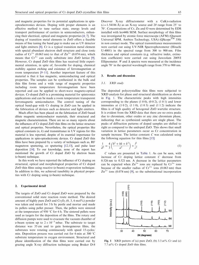
Fig. 1 XRD pattern of (a) pure ZnO, (b) 3.3 at% Cr and (c)
7.7 at% Cr doped ZnO thin films.
2. Experimental detail
The targets of ZnO and Cr doped ZnO were prepared by the
conventional solid state reaction route method. The desired
amount of highly pure ZnO and Cr2O3 (0, 3, 6 mol%) powder
was taken and mixed for 3 h by pestle and mortar and made
its pellets using pellet presser. Then, the pellets were sintered
at the temperature of 950 1C for 6 h. The sintered pellets were
used as targets for the deposition of the films. The rotary and
diffusion pumps were used to evacuate the vacuum chamber of
e-beam system up to 2� 10�5 mbar. The substrate to target
distance was 35 cm and to gain homogeneous films, the
substrates were rotating continuously with speed 15 cycles/
min. Deposition process was carried out for 6 min at 300 1C
substrate temperature in oxygen environment. Structural and
phase identification of the thin films were carried out by
grazing angle X-ray diffraction technique using Bruker D-8
Discover X-ray diffractometer with a CuKa-radiation(l¼1.54186 A) as an X-ray source and 2y range from 251 to
701. Concentrations of Cr, Zn and O were determined by EDS
installed with leo440i SEM. Surface morphology of thin films
was investigated by atomic force microscope (AFM) (Quesant
Universal SPM, Ambios Technology, USA) (QScopeTM 350)
in non contact mode. The optical transmittance measurements
were carried out using UV-NIR Spectrophotometer (Hitachi
U-4001) in the spectral range from 300 to 900 nm. Film
thickness and optical constants (e.g. refractive index, extinc-
tion coefficient) were carried out using Jawoolam 200VI
Ellipsometer. C and D spectra were measured at the incidence
angle 701 in the spectral wavelength range from 370 to 900 nm.
3. Results and discussion
3.1. XRD study
The deposited polycrystalline thin films were subjected to
XRD analysis for phase and structural identification as shown
in Fig. 1. The characteristic peaks with high intensities
corresponding to the planes (1 0 0), (0 0 2), (1 0 1) and lower
intensities at (1 0 2), (1 1 0), (1 0 3) and (1 1 2) indicate the
films is of high quality of hexogonal ZnO wurtzite structure.
It is evident from the XRD data that there are no extra peaks
due to chromium, other oxides or any zinc chromium phase,
indicating that as synthesized samples are single phase. The
peaks of diffraction patterns of doped samples are shifted to
right as compared to the undoped ZnO. This shows that small
variation in lattice parameters occur as Cr concentration in
sample increase. The lattice constant C was calculated using
the following equation for thin films [15]:
1
d2¼
4
3
h2 þ hkþ k2
a2
� �þ
l2
c2ð1Þ
C values are presented in Table 1. As can be seen, with
increase of Cr doping lattice constant C decrease from
0.526 nm to 0.521 nm. A decrease in the lattice parameters
can be expected when Zn2þ ions are replaced by Cr3þ ions
because of the smaller radius of Cr3þ ions (0.063 nm) than
Zn2þ ions (0.074 nm) [9], so the substitutional incorporation
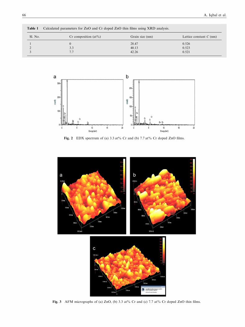
Table 1 Calculated parameters for ZnO and Cr doped ZnO thin films using XRD analysis.
Sl. No. Cr composition (at%) Grain size (nm) Lattice constant C (nm)
1 0 28.47 0.526
2 3.3 40.13 0.523
3 7.7 42.26 0.521
Fig. 2 EDX spectrum of (a) 3.3 at% Cr and (b) 7.7 at% Cr doped ZnO films.
Fig. 3 AFM micrographs of (a) ZnO, (b) 3.3 at% Cr and (c) 7.7 at% Cr doped ZnO thin films.
A. Iqbal et al.66
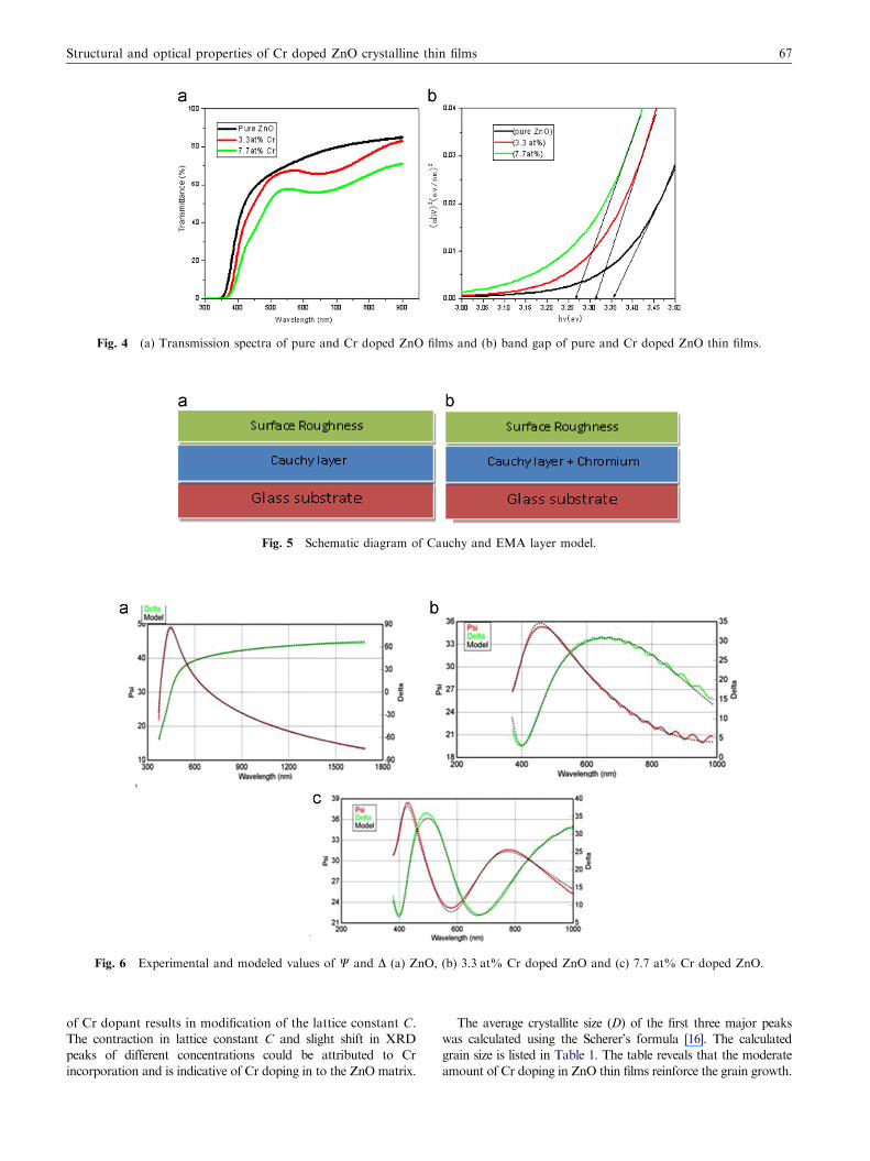
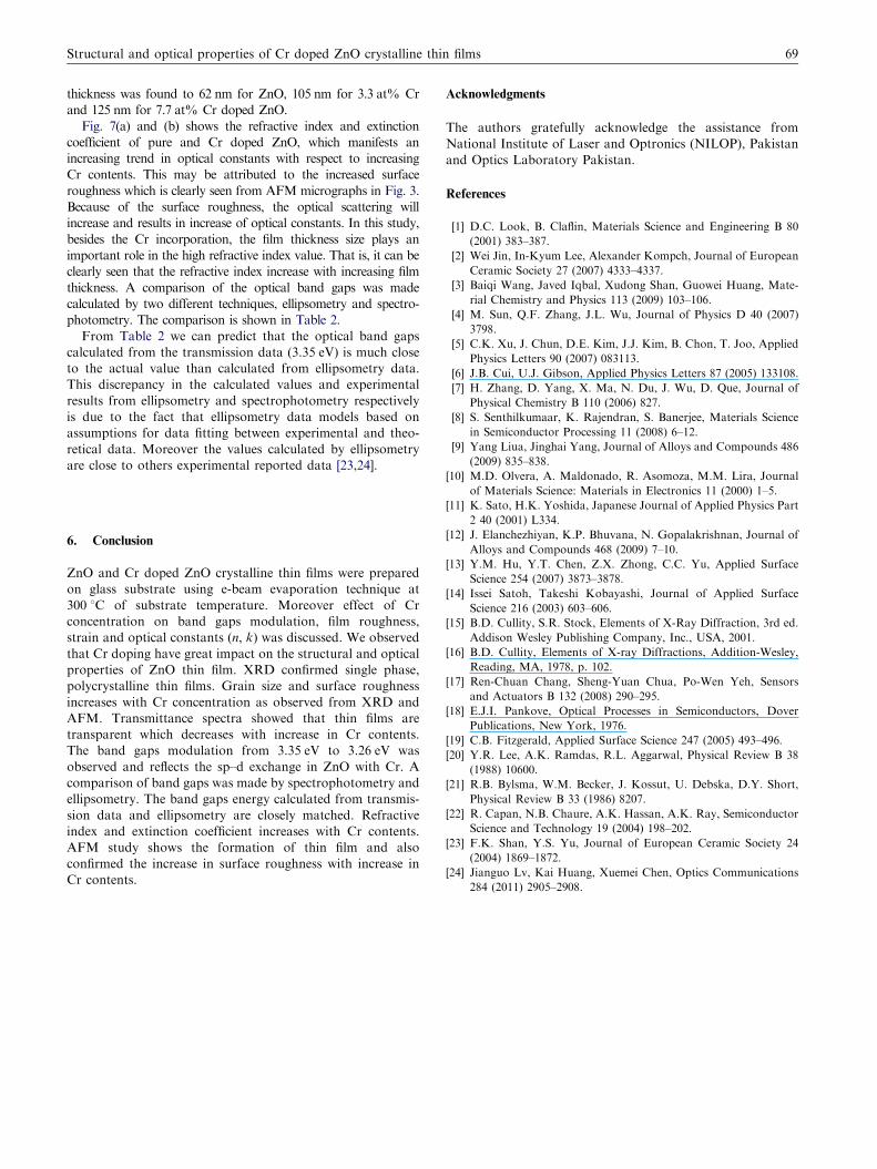
Fig. 5 Schematic diagram of Cauchy and EMA layer model.
Fig. 6 Experimental and modeled values of C and D (a) ZnO, (b) 3.3 at% Cr doped ZnO and (c) 7.7 at% Cr doped ZnO.
Fig. 4 (a) Transmission spectra of pure and Cr doped ZnO films and (b) band gap of pure and Cr doped ZnO thin films.
Structural and optical properties of Cr doped ZnO crystalline thin films 67
of Cr dopant results in modification of the lattice constant C.
The contraction in lattice constant C and slight shift in XRD
peaks of different concentrations could be attributed to Cr
incorporation and is indicative of Cr doping in to the ZnO matrix.
The average crystallite size (D) of the first three major peaks
was calculated using the Scherer’s formula [16]. The calculated
grain size is listed in Table 1. The table reveals that the moderate
amount of Cr doping in ZnO thin films reinforce the grain growth.

Fig. 7 (a) Variation of optical constants (a) refractive index and (b) extinction coefficient in Cr-doped ZnO thin films.
Table 2 Comparison of optical band gaps calculated by ellipsometry and spectrophotometry.
Sl. No. at% of Cr Band gap (eV) ellipsometry Band gap (eV) spectrophotometry
1 0 3.32 3.35
2 3.3 3.28 3.31
3 7.7 3.19 3.26
A. Iqbal et al.68
3.2. EDS analysis
The amount of Cr-doping was examined by EDS. Fig. 2(a) and
(b) shows the EDS spectrum of 3.3 at% Cr and 7.7 at% Cr
doped ZnO thin films respectively. From the figures it is well
evident that the deposited thin films consist of Cr, Zn and O
compositions. The presence of Si peak is due to glass substrate.
Therefore, the EDS results further indicate that Cr is incorpo-
rated in to ZnO, which is also, consistent with XRD results..
3.3. AFM study
Fig. 3(a–c) shows the AFM micrographs with scanning area of
1 mm� 1 mm for pure ZnO and Cr doped ZnO thin films,
respectively. All the samples have smooth morphologies with
root mean squared (RMS) roughness ranging from 5.06 nm to
24.04 nm. Similar results are observed by Ren-Chuan Chang
et al. in Mg doped ZnO thin films [17]. It is observed that the
RMS roughness increases with Cr doping which means the
surface becomes rough and grain size increases. The observed
increase in RMS with Cr doping may be due to no proper
agglomeration of crystallites..
4. Optical study
4.1. Spectrophotometry
Optical transmission spectra of the films were taken in the
wavelength of 300–900 nm using UV-NIR Spectrophotometer.
Fig. 4(a) displays the transmittance of pure and Cr doped ZnO
thin films. Transmission spectra of the samples divulge that
the transmittance decreases with Cr concentration which may
be due to the thickness of the films and doping effect. The
optical band gap energy (Eg) was determined from transmis-
sion measurements by analyzing the optical data with the
expression for the optical absorption coefficient, and the
photon energy hn using the following equation for direct band
gap materials [18]:
ðahnÞ2 ¼Aðhn�EgÞ ð2Þ
where a is the absorption coefficient, h is the Planck’s
constant, A is a constant and Eg is the optical band gap
energy. The optical band gap was obtained by extrapolating
the linear portion of the plots of (ahv)2 versus hn to a¼0. Forpure ZnO optical band gap was found to be 3.35 eV. We
observed the tuneability of the optical band gap from 3.35 eV
to 3.26 eV with Cr contents in ZnO material. Similar results
have also been reported for cobalt and Ni doped ZnO thin
films [19,20]. The decrease in the optical band gap in transition
metal doped II–IV semiconductor compounds has been
observed and can be best interpreted in terms of sp–d spin
exchange interaction between band electrons and the localized
d electrons of the transition metal ions substituting the cations
[19,21].
5. Spectroscopic ellipsometry
Film thickness and optical constants (e.g. refractive index,
extinction coefficient) were measured using spectroscopic
ellipsometry. C and D spectra were measured at the incidence
angle 701 in the spectral wavelength range of 370–900 nm.
Cauchy layer model was used for ZnO thin film to calculate
thickness and optical constants. Cauchy dispersion relation for
this model is given by the equation [22]:
n lð Þ ¼An þBn
l2þ
Cn
l4ð3Þ
The A, B, C parameters are variable fitted parameters that
determine the index dispersion. For Cr doped ZnO films effective
medium approximation (EMA) layer model was used to calculate
film thickness and optical constants. Fig. 5 shows the layer models
used for fitting experimental and theoretical data. Fig. 6 shows the
curve fitting for theoretical and experimental data. The film
Structural and optical properties of Cr doped ZnO crystalline thin films 69
thickness was found to 62 nm for ZnO, 105 nm for 3.3 at% Cr
and 125 nm for 7.7 at% Cr doped ZnO.
Fig. 7(a) and (b) shows the refractive index and extinction
coefficient of pure and Cr doped ZnO, which manifests an
increasing trend in optical constants with respect to increasing
Cr contents. This may be attributed to the increased surface
roughness which is clearly seen from AFM micrographs in Fig. 3.
Because of the surface roughness, the optical scattering will
increase and results in increase of optical constants. In this study,
besides the Cr incorporation, the film thickness size plays an
important role in the high refractive index value. That is, it can be
clearly seen that the refractive index increase with increasing film
thickness. A comparison of the optical band gaps was made
calculated by two different techniques, ellipsometry and spectro-
photometry. The comparison is shown in Table 2.
From Table 2 we can predict that the optical band gaps
calculated from the transmission data (3.35 eV) is much close
to the actual value than calculated from ellipsometry data.
This discrepancy in the calculated values and experimental
results from ellipsometry and spectrophotometry respectively
is due to the fact that ellipsometry data models based on
assumptions for data fitting between experimental and theo-
retical data. Moreover the values calculated by ellipsometry
are close to others experimental reported data [23,24].
6. Conclusion
ZnO and Cr doped ZnO crystalline thin films were prepared
on glass substrate using e-beam evaporation technique at
300 1C of substrate temperature. Moreover effect of Cr
concentration on band gaps modulation, film roughness,
strain and optical constants (n, k) was discussed. We observed
that Cr doping have great impact on the structural and optical
properties of ZnO thin film. XRD confirmed single phase,
polycrystalline thin films. Grain size and surface roughness
increases with Cr concentration as observed from XRD and
AFM. Transmittance spectra showed that thin films are
transparent which decreases with increase in Cr contents.
The band gaps modulation from 3.35 eV to 3.26 eV was
observed and reflects the sp–d exchange in ZnO with Cr. A
comparison of band gaps was made by spectrophotometry and
ellipsometry. The band gaps energy calculated from transmis-
sion data and ellipsometry are closely matched. Refractive
index and extinction coefficient increases with Cr contents.
AFM study shows the formation of thin film and also
confirmed the increase in surface roughness with increase in
Cr contents.
Acknowledgments
The authors gratefully acknowledge the assistance from
National Institute of Laser and Optronics (NILOP), Pakistan
and Optics Laboratory Pakistan.
References
[1] D.C. Look, B. Claflin, Materials Science and Engineering B 80
(2001) 383–387.
[2] Wei Jin, In-Kyum Lee, Alexander Kompch, Journal of European
Ceramic Society 27 (2007) 4333–4337.
[3] Baiqi Wang, Javed Iqbal, Xudong Shan, Guowei Huang, Mate-
rial Chemistry and Physics 113 (2009) 103–106.
[4] M. Sun, Q.F. Zhang, J.L. Wu, Journal of Physics D 40 (2007)
3798.
[5] C.K. Xu, J. Chun, D.E. Kim, J.J. Kim, B. Chon, T. Joo, Applied
Physics Letters 90 (2007) 083113.
[6] J.B. Cui, U.J. Gibson, Applied Physics Letters 87 (2005) 133108.
[7] H. Zhang, D. Yang, X. Ma, N. Du, J. Wu, D. Que, Journal of
Physical Chemistry B 110 (2006) 827.
[8] S. Senthilkumaar, K. Rajendran, S. Banerjee, Materials Science
in Semiconductor Processing 11 (2008) 6–12.
[9] Yang Liua, Jinghai Yang, Journal of Alloys and Compounds 486
(2009) 835–838.
[10] M.D. Olvera, A. Maldonado, R. Asomoza, M.M. Lira, Journal
of Materials Science: Materials in Electronics 11 (2000) 1–5.
[11] K. Sato, H.K. Yoshida, Japanese Journal of Applied Physics Part
2 40 (2001) L334.
[12] J. Elanchezhiyan, K.P. Bhuvana, N. Gopalakrishnan, Journal of
Alloys and Compounds 468 (2009) 7–10.
[13] Y.M. Hu, Y.T. Chen, Z.X. Zhong, C.C. Yu, Applied Surface
Science 254 (2007) 3873–3878.
[14] Issei Satoh, Takeshi Kobayashi, Journal of Applied Surface
Science 216 (2003) 603–606.
[15] B.D. Cullity, S.R. Stock, Elements of X-Ray Diffraction, 3rd ed.
Addison Wesley Publishing Company, Inc., USA, 2001.
[16] B.D. Cullity, Elements of X-ray Diffractions, Addition-Wesley,
Reading, MA, 1978, p. 102.
[17] Ren-Chuan Chang, Sheng-Yuan Chua, Po-Wen Yeh, Sensors
and Actuators B 132 (2008) 290–295.
[18] E.J.I. Pankove, Optical Processes in Semiconductors, Dover
Publications, New York, 1976.
[19] C.B. Fitzgerald, Applied Surface Science 247 (2005) 493–496.
[20] Y.R. Lee, A.K. Ramdas, R.L. Aggarwal, Physical Review B 38
(1988) 10600.
[21] R.B. Bylsma, W.M. Becker, J. Kossut, U. Debska, D.Y. Short,
Physical Review B 33 (1986) 8207.
[22] R. Capan, N.B. Chaure, A.K. Hassan, A.K. Ray, Semiconductor
Science and Technology 19 (2004) 198–202.
[23] F.K. Shan, Y.S. Yu, Journal of European Ceramic Society 24
(2004) 1869–1872.
[24] Jianguo Lv, Kai Huang, Xuemei Chen, Optics Communications
284 (2011) 2905–2908.
Copyright © 2022 FDOKUMEN