New crystalline silicon ribbon materials for photovoltaics
34
New crystalline silicon ribbon materials for photovoltaics G Hahn 1 and A Sch ¨ onecker 2 1 Department of Physics, University of Konstanz, Jakob-Burckhardt-Straße 29, 78457 Konstanz, Germany 2 ECN Solar Energy, PO Box 1, 1755ZG Petten, Netherlands E-mail: [email protected] Abstract The objective of this article is to review, in relation to photovoltaic applications, the current status of crystalline silicon ribbon technologies as an alternative to technologies based on wafers originating from ingots. Increased wafer demand, the foreseeable silicon feedstock shortage, and the need for a substantial module cost reduction are the main issues that must be faced in the booming photovoltaic market. Ribbon technologies make excellent use of silicon, as wafers are crystallized directly from the melt at the desired thickness and no kerf losses occur. Therefore, they offer a high potential for significantly reducing photovoltaic electricity costs as compared to technology based on wafers cut from ingots. However, the defect structure present in the ribbon silicon wafers can limit material quality and cell efficiency. We will review the most successful of the ribbon techniques already used in large scale production or currently in the pilot demonstration phase, with special emphasis on the defects incorporated during crystal growth. Because of the inhomogeneous distribution of defects, mapped characterization techniques have to be applied. Al and P gettering studies give an insight into the complex interaction of defects in the multicrystalline materials as the gettering efficiency is influenced by the state of the chemical bonding of the metal atoms. The most important technique for improvement of carrier lifetimes is hydrogenation, whose kinetics are strongly influenced by oxygen and carbon concentrations present in the material. The best cell efficiencies for laboratory-type (17%– 18%; cell area: 4 cm 2 ) as well as industrial-type (15%–16%; cell area: 80 cm 2 ) ribbon silicon solar cells are in the same range as for standard wafers cut from ingots. A substantial cost reduction therefore seems achievable, although the most promising techniques need to be improved. (Some figures in this article are in colour only in the electronic version) R1615 Konstanzer Online-Publikations-System (KOPS) URL: http://nbn-resolving.de/urn:nbn:de:bsz:352-2-1uhjxdajcjuz25 Erschienen in: Journal of Physics : Condensed Matter ; 16 (2004), 50. - S. R1615-R1648 https://dx.doi.org/10.1088/0953-8984/16/50/R03
-
Upload
khangminh22 -
Category
Documents
-
view
1 -
download
0
Transcript of New crystalline silicon ribbon materials for photovoltaics
New crystalline silicon ribbon materials forphotovoltaics
G Hahn1 and A Schonecker2
1 Department of Physics, University of Konstanz, Jakob-Burckhardt-Straße 29, 78457 Konstanz,Germany2 ECN Solar Energy, PO Box 1, 1755ZG Petten, Netherlands
E-mail: [email protected]
AbstractThe objective of this article is to review, in relation to photovoltaic applications,the current status of crystalline silicon ribbon technologies as an alternative totechnologies based on wafers originating from ingots. Increased wafer demand,the foreseeable silicon feedstock shortage, and the need for a substantialmodule cost reduction are the main issues that must be faced in the boomingphotovoltaic market. Ribbon technologies make excellent use of silicon, aswafers are crystallized directly from the melt at the desired thickness and no kerflosses occur. Therefore, they offer a high potential for significantly reducingphotovoltaic electricity costs as compared to technology based on wafers cutfrom ingots. However, the defect structure present in the ribbon silicon waferscan limit material quality and cell efficiency.
We will review the most successful of the ribbon techniques already usedin large scale production or currently in the pilot demonstration phase, withspecial emphasis on the defects incorporated during crystal growth. Because ofthe inhomogeneous distribution of defects, mapped characterization techniqueshave to be applied. Al and P gettering studies give an insight into the complexinteraction of defects in the multicrystalline materials as the gettering efficiencyis influenced by the state of the chemical bonding of the metal atoms. Themost important technique for improvement of carrier lifetimes is hydrogenation,whose kinetics are strongly influenced by oxygen and carbon concentrationspresent in the material. The best cell efficiencies for laboratory-type (17%–18%; cell area: 4 cm2) as well as industrial-type (15%–16%; cell area:�80 cm2) ribbon silicon solar cells are in the same range as for standardwafers cut from ingots. A substantial cost reduction therefore seems achievable,although the most promising techniques need to be improved.
(Some figures in this article are in colour only in the electronic version)
R1615
Konstanzer Online-Publikations-System (KOPS) URL: http://nbn-resolving.de/urn:nbn:de:bsz:352-2-1uhjxdajcjuz25
Erschienen in: Journal of Physics : Condensed Matter ; 16 (2004), 50. - S. R1615-R1648 https://dx.doi.org/10.1088/0953-8984/16/50/R03

R1616
Contents
1. Introduction 16161.1. Electronic characteristics 16181.2. Impurities 1619
2. Ribbon silicon wafers 16192.1. Classification of ribbon technologies 16192.2. The silicon ribbon growth mechanism, crystal structure, and machine
throughput 16202.3. Refractory materials and impurities 16222.4. Examples of different ribbon technologies 1624
3. Defects 16263.1. Material properties 1626
4. Gettering 16304.1. Gettering techniques 16304.2. Gettering in EFG and SR materials 16314.3. Gettering in RGS material 1632
5. Hydrogen passivation 16325.1. Interaction with defects 16335.2. Methods for hydrogen incorporation 16345.3. Passivated defects and stability 16345.4. Hydrogenation of EFG and SR materials 16345.5. Hydrogenation in RGS material 16355.6. Diffusion of H in defected silicon 1636
6. Ribbon silicon solar cells 16386.1. Laboratory-type and industrial-type processing 16386.2. EFG and SR solar cells 16396.3. RGS solar cells 16416.4. Summary 1642References 1644
1. Introduction
In recent years the photovoltaic (PV) market has seen explosive growth with annual rates wellabove 30%. In 2003, solar cell production exceeded 700 MWp3 [1]. As more than 90% of allphotovoltaic modules are silicon wafer based, this required more than 250 million wafers. Thehigh market growth rate in combination with the need to substantially reduce solar electricitycosts has resulted in a number of serious challenges for silicon wafer production developmentfor photovoltaics. If today’s trends can be extrapolated into the near future, we can expect thatby 2010 the PV market will consume about 30.000 t of solar grade silicon to produce solarsilicon wafers. This is more than the silicon semiconductor industry consumes today.
In order to meet these challenges, it is very likely that wafer manufacturing technologyaimed at the photovoltaics market will continue to develop. The following requirements mustbe met:
• low silicon consumption (thinner wafers, reduction or elimination of wafer cutting losses),• reduced investment requirements as regards crystal growth and wafer cutting equipment
(high production speed, high machine up-time, inexpensive machines),3 Equivalent electrical power under standard test conditions. The typical cell output is 2.5 Wp; a photovoltaic moduleproduces between 50 and 150 Wp.

R1617
• increased wafer size (reduced processing per Wp),
• sufficient silicon quality to produce highly efficient solar cells.
Although the demand is very clear, the technological roadmap for meeting the aboverequirements is not clear. On one hand, existing technologies are continuously improved bymeans such as achieving faster growth of multicrystalline silicon ingots, producing largeringots with more silicon in one crystallization step, and melt recharging in the case ofCzochralski (Cz) crystal pulling. On the other hand, new, promising high speed silicon wafermanufacturing technologies are under development in order to meet the requirement of lowsilicon consumption in combination with high production speed.
In principle, the most promising wafer manufacturing technologies are the ones whereliquid silicon is directly crystallized in the form of a silicon wafer or ribbon (so-called ribbontechnologies). In order to enable a successful introduction of high speed ribbon silicon wafertechnologies, however, the challenge is to reach sufficient wafer quality and solar cell efficiencyto make a major contribution to future solar electricity cost reduction.
In the following, an overview of advanced ribbon silicon wafer manufacturing technologiesfor photovoltaics is given, with emphasis on silicon material properties in relation to the growthprocess and silicon material quality improvement by gettering and passivation proceduresduring wafer growth and solar cell processing.
Looking back into the history of photovoltaic silicon wafers, we find that early wafersoriginated from semiconductor silicon wafer processes (float zone or Cz). Due to the pressureon manufacturing costs and the reduced demands for wafer characteristics such as surfacemorphology, contamination, and thickness variation, dedicated wafer manufacturing lines forthe photovoltaic industry were established. This resulted in wafers that differ in many respectsfrom a typical semiconductor wafer [2, 3].
The technological basis for many of today’s photovoltaic silicon ingot growth technologiesas well as silicon ribbon technologies was developed in flat panel solar array projects [4].Due to the very successful development of cost-efficient wafer cutting by multiwire sawingtechnologies, today’s market is based on silicon ingot growth (Cz ingots, multicrystallinesilicon ingots grown by SOPLIN [5], electromagnetic casting (EMC) [6], Bridgman–Stockbarger, and similar methods). A major drawback of silicon ingot casting and wafercutting is the severe silicon loss due to kerf loss, rejection of tops, tails, and silicon parts thatwere in contact with the crucible. A silicon yield of less than 40% is typical for many ofthe silicon ingot growth technologies [7] and measures are taken in industry to reduce siliconlosses in the ingot process. As wafer costs represent 40%–50% of the cost of a PV module,wafer manufacturing technologies with low costs and high silicon yield per solar electricalpower output are an important milestone in the race to lower the cost of solar electricity.
In general, silicon wafer based solar energy technology follows a twofold strategy toreduce the costs of solar electricity. One approach is increasing the power output per area(i.e. conversion efficiency); the other is lowering manufacturing costs. As solar modules arearea based devices with an energy conversion efficiency in the 15%–16% range and as thethermodynamic conversion limit for single-junction solar cells under terrestrial conditions is31% [8], efficiency improvements have a cost reduction potential of at maximum 50%, with25% being more likely (record efficiencies for Si solar cells are in the 24%–25% range [9]).Hence efficiency improvement in itself is not sufficient to reach the demanding cost targets.The second and possibly larger cost reduction potential lies in reducing the manufacturingcosts for not only wafer manufacturing but also all other steps throughout the productionchain. If high speed, low cost processes for wafer manufacturing, solar cell processing, andmodule packaging can be developed, the module costs will approach the limit imposed by the

R1618
materials in the solar module. In this respect, the application of a silicon ribbon technologywith corresponding high silicon usage without compromising the conversion efficiency willbe one step necessary to realize the ultimate silicon wafer based solar module.
1.1. Electronic characteristics
The most important electronic characteristics of a silicon wafer for use in a solar cell are theresistivity in the dark and the minority charge carrier lifetime. However, in contrast to the casefor cast silicon wafers or Cz material, the as-grown characteristics of ribbon silicon material areslightly different. The resistivity of the wafer, which is determined by the type and amount ofdoping material that is added during crystal growth, is normally lower than for other wafers forsolar applications. If boron doping is used, it turned out that the highest efficiency for ribbonsilicon material is reached for 2–3 � cm material, while cast silicon material is typically dopedwith boron in the 0.5–2 � cm range.
The same is true for the minority carrier lifetime. Typical as-grown lifetimes for ribbonsilicon are lower than those for cast and Cz doped wafers. Ribbon silicon wafers thereforedepend upon solar cell processing steps for improving their electrical characteristics duringthe solar cell processing (gettering and passivation). Thus monitoring the minority carrierlifetime and diffusion length (respectively) throughout the solar cell processing has proven tobe valuable in the development of ribbon materials.
The minority charge carrier lifetime, τ , or, related to it via
Ldiff = √Dτ , (1)
the minority charge carrier diffusion length, Ldiff , is a measure of the mean time or distance,respectively, that a charge carrier can travel before it is lost via a recombination process(D being the minority carrier diffusion constant). While there are different charge carrierrecombination processes such as Auger recombination and recombination by emission of aphoton possible in silicon, under typical operating conditions for a solar cell the most probablerecombination mechanism is recombination via an energy level in the band gap. This isoften referred to as Shockley–Read–Hall recombination [10, 11]. The recombination rate,R, is strongly influenced by the energy level of the recombination centre, the capture crosssection for electrons and holes, and the recombination centre concentration (see equation (2));recombination centres can originate from crystallographic defects, impurities, or combinationsof the two:
R = vth Nt (np − n2i )
1σp
(n + n1) + 1σn
(p + p1). (2)
vth is the thermal velocity, Nt is the recombination centre density, n (p) is the electron (hole)concentration, ni is the intrinsic carrier concentration, σn (σp) is the capture cross section forelectrons (holes);
n1 = ni exp
(Et − Ei
kT
)(2a)
p1 = ni exp
(Ei − Et
kT
)(2b)
with Et the energy of the recombination centre, Ei the intrinsic energy level.The carrier lifetime, τ , is related to the recombination rate by
τ = �n
R(3)
with �n being the excess carrier density.
R1619
1.2. Impurities
Impurities are non-silicon atoms or clusters of atoms incorporated into the silicon crystal orwafer. One necessary impurity in the silicon wafer is the doping material. Other impuritiesoriginate from contamination during crystal growth, the silicon material used, or from handlingof the silicon in the manufacturing process. The impurities with the highest concentrationsin silicon wafers are typically oxygen and carbon. They can originate from silicon material(SiO2, C) in the case of low quality solar grade silicon or from refractory material (quartzor graphite crucibles) used during silicon processing. Typical concentrations of oxygen andcarbon in silicon wafers used in photovoltaics are between 1 × 10¹⁷ and 1 × 1018 cm−3.
Other ‘metallic’ impurities are also found in photovoltaic wafers. Depending on the typeof metal, even very low concentrations can have a negative influence on the minority carrierlifetime and solar cell efficiency [12, 13].
The behaviour of impurities in silicon and their influence on wafer quality and processtechnologies for impurity treatment (impurity gettering, passivation) constitutes a major topicin silicon research.
2. Ribbon silicon wafers
Driven by the motivation of increasing the Si yield in wafer manufacturing and avoiding thetime- and energy-consuming and therefore costly steps of ingot growing and wafer cutting,research into and development of methods for crystallizing silicon directly in the planar formof a wafer have been going on for four decades [14–34] (see [35] for an early overview). Itwas only recently that some of the ribbon technologies reached maturity, and manufactureon a megawatt scale, such as in the cases of the edge-defined film-fed growth (EFG [36])and the string ribbon (SR [37]) technologies, could emerge. Other technologies such as thesilicon film [38], dendritic web [14], ribbon growth on substrate (RGS [30]) and rotationalsolidification techniques [33, 34] are under development at pilot demonstration phases.
2.1. Classification of ribbon technologies
To understand the potential of the different photovoltaic silicon ribbon technologies, a closerlook at the wafer growth technology, wafer characteristics, and behaviour in the cell processis necessary.
In the past, the different ribbon Si technologies were classified in several ways:
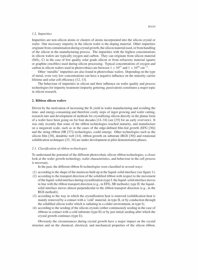
(1) according to the shape of the meniscus built up at the liquid–solid interface (see figure 1);(2) according to the transport direction of the solidified ribbon with respect to the movement
of the liquid–solid interface during crystallization (type I: the liquid–solid interface movesin line with the ribbon transport direction (e.g., in EFG, SR methods); type II: the liquid–solid interface moves almost perpendicular to the ribbon transport direction (e.g., in theRGS method));
(3) according to the way in which the crystallization heat is removed (solidification heat ismainly removed by a contact with a ‘cold’ material, in type II, or by conduction throughthe solidified silicon wafer which is radiating in a colder environment, in type I);
(4) according to the seeding of the silicon crystals (either continuously seeding in the case ofribbons in contact with a cold substrate (type II) or by just initial seeding after which thecrystal growth continues (type I)).
Obviously the circumstances during crystal growth have a major impact on the crystalstructure and on the chemical, electrical, and mechanical properties of the silicon ribbon.
R1620
Figure 1. Classification of silicon ribbon technologies according to the shape of the meniscusat the liquid–solid interface [35]. For M1 the lower part of the meniscus is formed by a shapingdie, whereas M2 has a broad base at the free surface of the liquid. Both M1 and M2 representribbon techniques where the crystallization moves in the direction of ribbon transport (type I). M3is characterized by a large liquid–solid interface and represents the techniques with wafer transportalmost perpendicular to the crystal growth direction (type II).
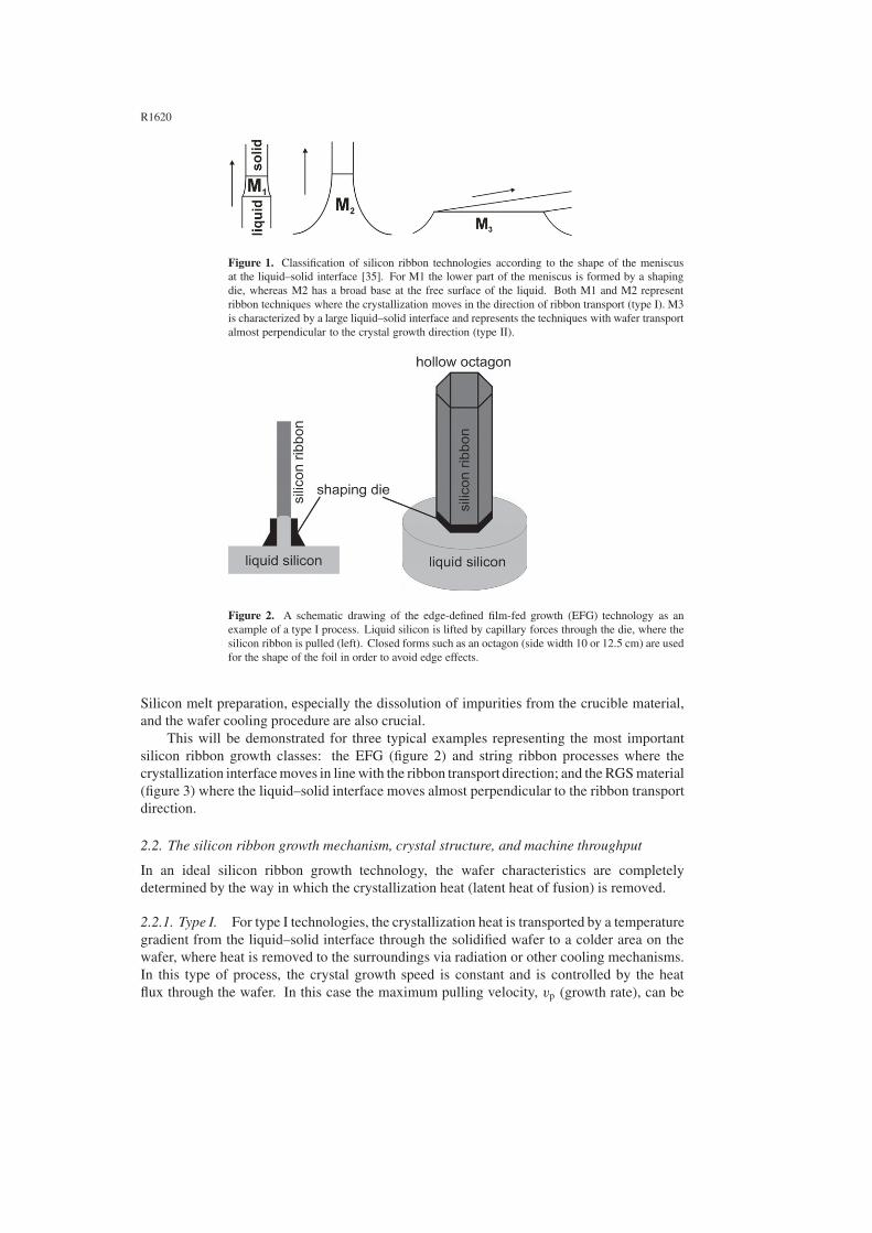
Figure 2. A schematic drawing of the edge-defined film-fed growth (EFG) technology as anexample of a type I process. Liquid silicon is lifted by capillary forces through the die, where thesilicon ribbon is pulled (left). Closed forms such as an octagon (side width 10 or 12.5 cm) are usedfor the shape of the foil in order to avoid edge effects.
Silicon melt preparation, especially the dissolution of impurities from the crucible material,and the wafer cooling procedure are also crucial.
This will be demonstrated for three typical examples representing the most importantsilicon ribbon growth classes: the EFG (figure 2) and string ribbon processes where thecrystallization interface moves in line with the ribbon transport direction; and the RGS material(figure 3) where the liquid–solid interface moves almost perpendicular to the ribbon transportdirection.
2.2. The silicon ribbon growth mechanism, crystal structure, and machine throughput
In an ideal silicon ribbon growth technology, the wafer characteristics are completelydetermined by the way in which the crystallization heat (latent heat of fusion) is removed.
2.2.1. Type I. For type I technologies, the crystallization heat is transported by a temperaturegradient from the liquid–solid interface through the solidified wafer to a colder area on thewafer, where heat is removed to the surroundings via radiation or other cooling mechanisms.In this type of process, the crystal growth speed is constant and is controlled by the heatflux through the wafer. In this case the maximum pulling velocity, vp (growth rate), can be

R1621
Figure 3. A schematic drawing of the ribbon growth on substrate (RGS) process, typical of type IItechnology. Preheated substrates are transported at the ribbon pulling speed underneath a castingframe filled with liquid silicon. The crystallization heat is removed into the ‘cold’ substrate anda 300–400 μm thick silicon film is grown. After the silicon ribbon is removed, the substrate isre-used in the process.
calculated as
vp = 1
Lρm
(σε(W + t)KmT 5
m
Wd
)1/2
(4)
with L being the latent heat of fusion, ρm the density of the crystal at the melting temperature,σ the Stefan–Boltzmann constant, ε the emissivity of the crystal, Km the thermal conductivityof the solid crystal at the melting temperature Tm, W the ribbon width, and d the ribbonthickness [39]. For 300 μm thick ribbons, equation (4) predicts a maximum growth rate of∼8 cm min−1.
Actual growth rates are much lower due to the maximum tolerable thermal stress limitingthe maximum tolerable temperature gradient in the ribbon. The temperature gradient thatis reached in the silicon ribbon is around 1000 ◦C cm−1 close to the liquid–solid interface(for EFG [40]). This gradient causes stress, which increases with d2T/dy2 (y is the growthdirection). The resulting dislocation formation and buckling are critical, limiting the realizedgrowth speeds to ∼2 cm min−1 for plane ribbons of ∼300 μm thickness, and to somewhatlower speeds for thinner ribbons (compared to the theoretical value of ∼8 cm min−1). Thethermal environment around the newly formed ribbon above the crucible is crucial for thestress. Stacks of thermal shields and after-heaters are used to control and reduce stress [41].The best approach is to confine stress as much as possible to the liquid–solid interface, whereplastic flow can occur.
As the crystal growth is based upon the crystal structure of the already solidified silicon, thesilicon ribbon exhibits long crystals in the ribbon growth direction with horizontal dimensionsfrom the millimetre to centimetre range. Rapidly growing crystal orientations are preferred.Depending on the growth velocity and initial seeding, even monocrystalline material ispossible [14].
2.2.2. Type II. In the case of type II silicon ribbons, the heat is removed from the liquid–solidinterface through the solidified wafer into the cold substrate. Compared with the case for typeI technologies, heat removal through the thin wafer with a large cross section is more effective,resulting in a much higher growth rate.

R1622
In this case, the ribbon growth speed can be expressed as
vp = 4αKms
(2Km − αt) dLρm�T (5)
where α is the effective coefficient of heat transfer, s the length of the liquid–solid interface (inthe pulling direction), and �T the temperature gradient between the melt and the substrate [30].For �T = 160 ◦C, equation (5) predicts maximum growth rates of the order of 600 cm min−1.This indicates that techniques with a large liquid–solid interface have the potential for veryhigh pulling rates and therefore a higher throughput as compared to techniques of type I.
Due to the silicon crystal growth being in contact with the substrate, type II ribbons havecompletely different characteristics to type I ribbons. As crystal seeding takes place on thesubstrate, the wafers typically have small, columnar grains with random orientation. Thecrystal growth velocity is time dependent. The position of the liquid–solid interface followsa square-root dependence with faster initial crystal growth velocity when the liquid siliconis in direct contact with the substrate, and slower growth occurring with increasing thicknessof the wafer due to the additional heat transport through the solidified silicon. The principleof the type II crystal growth can be described via the ‘classical Stefan problem’ [42]. Thisassumes that a liquid at uniform temperature Tl, which is higher than the melting temperatureTm, is confined to a half-space x > 0. At time t = 0 the boundary surface (x = 0) is loweredto a temperature T0 below the melting temperature (i.e. contact with the cold substrate) andmaintained at this temperature. As a result, solidification starts at the surface x = 0 and aliquid–solid interface s(t) moves in the positive x-direction. Under these assumptions, theheat conduction equations can be solved and the position s(t) of the liquid–solid interface astime varies is described by
s(t) = λ√
αst (6)
where αs is the thermal diffusivity of the solid phase and λ is the solution to the equation
exp(λ2/4)
erf(λ/2)+
b√a
Tm − Tl
Tm − T0
exp(−λ2/4a)
erfc(λ/2√
a)− λ
√πhsf
2cps(Tm − T0)= 0 (7)
with the following parameters: b is the ratio of liquid to solid heat conductivity, a is ratio ofliquid to solid heat diffusivity, L is latent heat of fusion, and cps is the specific heat capacityof the solid phase.
In general, crystal growth is more complex than that of the system outlined above due to thebehaviour of T0 (the temperature at the bottom of the solidified wafer), which in general is notconstant, the temperature dependence of the material characteristics, and the often turbulentflow in the liquid silicon melt. The variable growth speed results in thickness dependentmaterial characteristics due to processes such as velocity dependent effective segregation ofmetallic impurities.
In contrast to the case for type I crystal growth, where a relatively large temperaturegradient in the solidified silicon is the driving force for crystallization, the temperature gradientthrough the solidified silicon in type II processes can be very small. Therefore, it is in principlepossible to grow wafers with lower thermal stress, provided that other process parameters suchas wafer cooling and other mechanical stresses are controlled.
2.2.3. Comparison of growth techniques. See table 1.
2.3. Refractory materials and impurities
In addition to the crystallization conditions, the materials that are used in ribbon growthequipment and the atmospheric environment are important factors influencing the wafer

R1623
Table 1. Some data related to the crystal growth by SR and EFG (type I) and RGS (type II)methods.
Type I Type II
Angle between crystal growth 180◦ Almost 90◦direction and ribbon transport
Typical ribbon growth 1–2 cm min−1 600 cm min−1
velocities
Typical annual wafer output ∼0.5 mill. wafer/machine ∼20 mill. wafer/machine
Crystallization velocity Constant (1–2 cm min−1) Variable (mean 2 cm min−1)
Crystal size Extended crystals in pulling 100 μm to 1 mm rangedirections, mm to cmdimensions perpendicularto pulling direction
Crystal orientation EFG: close to {011} [43, 44] Random
Thermal stress High (tolerable thermal stress Lowlimits growth velocity)
characteristics. In most ribbon technologies the solidification area is in close proximity tothe refractory materials (such as the shaping die for EFG or the casting frame and substratefor RGS). In contrast to the case for ingot casting, it is not possible to discard the siliconthat was crystallized in contact with the refractory material. In addition, other technologiessuch as SiO evaporation in the Cz process are not possible due to the close proximity of thecrystallization process to refractory material. Therefore, much research has gone into thedevelopment of silicon resistant refractory materials with the aim of minimizing the resultingcontamination [45]. The result was the finding that most ceramic materials produced incombination with metal oxide binders cannot be used due to the very low contaminationtolerance of silicon wafers to metallic impurities [12, 13]. The same is true for ceramicsincluding doping elements such as B (in BN) or Al (in SiAlON). Today, only quartz [46]and graphite based crucibles [47] are in common use as refractory materials. Most ribbongrowth technologies rely on graphite components due to the mechanical and thermal propertiesof the material, the good availability of semiconductor grade material, and the relativelyhigh tolerance of silicon to graphite contamination. Understanding the dissolution reactionand solubility limits of refractory materials and impurities therein has been crucial in thedevelopment of silicon ribbons and is needed to understand the characteristics of the material.
The behaviour of quartz crucibles and the interaction with liquid silicon were examinedthoroughly with a view to controlling the oxygen content in Cz wafers [48]. The importantinteraction of liquid silicon with graphite crucibles and the formation of a SiC interface layerconstitute a topic of ongoing research that is important for the further development of siliconribbons. It is generally assumed that the initial contact of pure liquid silicon with graphiteleads to the dissolution of graphite in the silicon [49]. From reactive wetting experiments thereare indications that this dissolution of graphite is a very rapid process, as is the diffusion ofcarbon in liquid silicon [50, 51]. Normally, this behaviour should result in a carbon saturatedsilicon melt, but scanning electron microscopy analyses of the silicon–graphite interface showthe existence of a SiC layer at the interface [52]. The growth of the SiC layer takes place intwo different growth regimes: in the initial one with the linear kinetics of an interface reactionlimited process, followed by a slower process with approximately parabolic kinetics, whichcan be explained by a growth process that is limited by carbon diffusion through the SiC layer.

R1624
Therefore, after the initial growth of the SiC interface layer, the further dissolution of carbonfrom the graphite crucible is kinetically hindered by diffusion through a SiC interface layer.
Of high technological interest is the carbon concentration in the wafers in relation tothe growth conditions. Experiments [53] show that the solubility of carbon in liquid siliconequilibrated with SiC can be described by
log
([C]
mass%
)= 3.63 − 9660
Tfor T : 1723–1873 K. (8)
At the silicon melting point, this should result in carbon concentrations of 9.1×1018 cm−3.As the carbon solubility in solid silicon is 3.5 × 1017 cm−3 at the melting point of Si, the highcarbon solubility in the liquid silicon should result in carbon supersaturated solidified siliconor the formation of SiC either residually in the melt or incorporated in the silicon crystal.
Despite the high level of dissolution of carbon in liquid silicon, it is technically possibleto produce silicon ribbons with substitutional carbon concentrations lower than 1×1018 cm−3
or even in the 5 × 1017 cm−3 region in a graphite environment [47]. As carbon contaminationis important for the electrical and mechanical properties of the silicon wafer, the growth ofsilicon ribbons with carbon content well below the liquid solubility is very much desired.
2.4. Examples of different ribbon technologies
In the following we will focus on the silicon ribbon technologies that were most widely studiedin the past. The edge-defined film-fed growth and string ribbon methods were chosen as typicalrepresentatives of type I silicon ribbon technologies and ribbon growth on substrate as the typeII technology.
2.4.1. Edge-defined film-fed growth (type I technology). In the EFG process commercializedat Mobil Tyco and ASE (now RWE Solar), the silicon ribbon is pulled to heights of up to7 m from the top of a graphite die (shape of meniscus: M1) through which molten silicon isfed by capillary action. Extensive temperature control by radiation shields, cold shoes, andafter-heating realizes a maximum temperature gradient where plastic flow is possible, in orderto allow for a maximum growth rate as described above [54, 55].
The silicon is contained in a graphite crucible, which contains only about 1 kg of silicon.It is continuously replenished, with up to 200 kg Si supplied during a growth run. The solidsilicon ribbon is (super)saturated with carbon but contains very little oxygen. Crystal graindimensions are typically of the order of a few mm in width but can reach great lengths in thecrystal growth direction. The as-grown diffusion length is related to the purity of the graphiteparts. The tubes (octagons) are cut into wafers (10 × 10, 10 × 15, or 12.5 × 12.5 cm2) by alaser.
2.4.2. The string ribbon process (type I). The string ribbon technology (figure 4) was inventedat the National Renewable Energy Laboratory and at Arthur D Little, commercialized byEvergreen Solar Inc. It uses high temperature resistant strings, which are drawn at a distanceof 8 cm through a crucible with liquid silicon. They pull up a Si meniscus (M2) of about7 mm height, which crystallizes to become the ribbon. In comparison to the case for the EFGtechnique (where temperature near the liquid–solid interface must be controlled to ±1 K),temperature control near the liquid–solid interface is less critical (±10 K is tolerated) and thisallows the use of more cost-effective furnace designs [37].
The result is a silicon ribbon with a typical dislocation density of less than 105 cm−2.The main defects in the central area of the ribbon are twins, and at the edges high angle

R1625
Figure 4. A schematic drawing of the string ribbon (SR) process. Two strings are pulled throughthe silicon melt. They define the edges of the silicon film.
grain boundaries occur due to heterogeneous nucleation. The typical grain size for 300 μmthick ribbons is around 1 cm or even larger for thinner ribbons. As with EFG, the oxygenconcentration is low, but the carbon concentration is reduced.
Like in the EFG case, an after-heater construction around the crystallization area is usedto reduce thermal stress [41]. As for EFG material production, the string ribbon technologyuses a small silicon melt crucible in combination with continuous melt replenishment. To helpovercome the problem of limited throughput of only one ribbon per furnace, compared to eightribbons in the octagon for EFG, two ribbons [56] (and even four with a recently publishednew crucible design [57]) can be grown simultaneously in one furnace. The ribbon is cut into8 × 15 cm2 wafers.
2.4.3. Ribbon growth on substrate (type II). The principle of the ribbon growth on substrate(RGS) process is that a series of graphite based substrates move at high velocity (typically10 cm s−1 or 6 m min−1) under a casting frame, which contains liquid silicon, and defines thesize of the wafers and the solidification front.
The crystal growth speed can be controlled by the heat extraction capacity of the substratematerial. During cooling, the difference in thermal expansion coefficient between the substratematerial and Si ribbon causes a separation of the silicon ribbon from the substrate and allowsthe re-use of the substrate material.
In the former laboratory scale wafer manufacturing process, RGS wafers werecharacterized by an extremely high oxygen content of 2–4×1018 cm−3, which limited the solarcell efficiency [58]. Unless the wafers are quenched to room temperature in a few secondsafter solidification, the oxygen will mostly (>90%) precipitate (e.g. as recombination activenew donors formed at 600–900 ◦C or, when cooling more slowly, as larger precipitates [59]).This precipitation is enhanced by the high carbon content. There have been two approachesfor producing RGS wafers that could be used in a solar cell process. The first of these wasproduction of quench-cooled wafers, which have a high interstitial oxygen content and thereforehave to be processed avoiding new donor formation, which takes place at temperatures between

R1626
600 and 900 ◦C. Such wafers are not suited for ‘standard’ solar cell processes. The otherapproach was precipitating the oxygen in the form of large clusters via a high temperaturetreatment. In this case, the wafers could be processed in a temperature range between 600 and900 ◦C and standard cell processing could be applied. The drawback of the latter method isa prolonged annealing step at temperatures >1000 ◦C directly after crystallization which wasnot practicable in the planned industrial-type wafer fabrication.
Just recently, it has been found that the high oxygen content can be significantly reducedto values of 5–7 × 1017 cm−3 by changing the crucible design (replacing quartz componentsby graphite parts). This reduction has resulted in a material quality allowing standard solarcell processing temperature cycles with RGS wafers rapidly cooled after crystallization [58].
The RGS method was developed by Bayer AG in the 1990s. It is now under developmentin a cooperation between Deutsche Solar AG and a consortium of the Energy Research Centreof the Netherlands and Sunergy.
3. Defects
As nearly all of the ribbon silicon growth techniques developed result in multicrystallinematerial, crystal defects play a major role in the solar cell efficiencies obtained for ribbonsilicon wafers. There is a general trend for higher defect concentrations with faster ribbongrowth, but even within wafers obtained by one growth technique there is an inhomogeneousdefect distribution. In this section, we will subject the known relevant defects for the three typesof material (produced by EFG, SR, and RGS processes) to closer examination. Interactionbetween different types of defect must be taken into account and for one example we will discussthe possibility of making use of certain kinds of defects to improve solar cell efficiency.
3.1. Material properties
The specific growth conditions for the silicon ribbons result in the material properties listedin table 2. EFG and SR materials both have grains elongated in the growth direction in thecentimetre range with a tendency towards larger grains for SR material. Twinning occursfrequently within the grains, but does not necessarily reduce the carrier lifetime or diffusionlength, Ldiff . The ribbon thickness for all technologies is ∼300 μm, and therefore comparablewith that of standard ingot cast wafers. The resistivities due to boron doping are slightly higherthan for ingot cast wafers, and are in the 2–4 � cm range. The higher optimum resistivitythan used for standard ingot cast multicrystalline wafers (∼1 � cm) may be related to the highcarbon concentration. A possible recombination centre involving both boron and carbon mightbe responsible for the observed material degradation detected for lower resistivity material [60],although the underlying defect has not yet been identified.
EFG and RGS materials share very high carbon concentrations due to the contact withgraphite-containing materials near the liquid–solid interface (die or substrate). The oxygenconcentration is very low for EFG and SR materials, and high for RGS material. The grain sizeis smaller for RGS material (0.1–0.5 mm) as there are more nucleation sites on the substrate.The dislocation density in RGS material generally tends to be higher than those for EFG andSR materials, which means that the possibility of stress free wafer growth is not yet fullyrealized.
Additionally, transition metals are present in all materials, although mostly inconcentrations not limiting material quality. Nevertheless, some are effective recombinationcentres such as point defects or in the form of precipitates, and affect the as-grown materialquality.

R1627
Table 2. Properties of materials produced by the three ribbon techniques under close consideration.
Grain Dislocation Thickness Resistivity [C] [O] As-grownMaterial size density (cm−2) (μm) (� cm) (cm−3) (cm−3) Ldiff (μm)
EFG cm 104–105 300 2–4 1018 <5 × 10¹⁶ 10–300SR cm 104–105 300 3 5 × 10¹⁷ <5 × 10¹⁶ 10–300RGS <mm 105–107 300 2 1018 1018 ∼10
The effects of an isolated defect on material quality (e.g. recombination activity of aclean, undecorated dislocation, capture cross sections of point defects) are well known formany defects present in crystalline silicon material, but the interactions of the impuritiesor structural defects form a major challenge in obtaining an improved understanding of thecomplex situation in the solidified silicon ribbon. In the following sections, some of theseinteractions are addressed. As EFG and SR materials are very similar, they will be dealt within the same section, although most of the results have been obtained for EFG material.
3.1.1. EFG and SR materials.
Stress and dislocations. Ribbon technologies with the plane of the liquid–solid interfaceperpendicular to the growth direction all suffer from built-in stress due to the varying thermalgradient in the solidified ribbon [61]. This stress can lead to the formation of areas with highdislocation density. In these areas carrier lifetimes are reduced as shown by photoluminescencespectroscopy [62, 63] and transmission electron microscopy (TEM). High stresses can bedetected also in areas with a low dislocation density [64]. Areas only containing twins withoutincreased dislocation densities do not show reduced lifetimes. They are, however, highlystressed and there is evidence that this might be due to incorporation of carbon into the twinboundaries [65].
It is known that clean dislocations without decoration reveal almost no recombinationactivity [66] but increasing decoration with impurities leads to recombination centres deep inthe band gap which significantly reduce the carrier lifetime [67]. It can therefore be concludedthat the most detrimental defects in EFG and SR materials apart from recombination activelarge angle grain boundaries are decorated dislocations.
Microdefects. Other types of defects are also present in EFG and SR materials. The V/Gratio of EFG and SR materials (with V being the growth speed and G the liquid–solid interfacetemperature gradient) is comparable to that of the microdefect regime of D swirls in floatzone growth [60]. Kalejs assumes that due to the high [C]/[O] ratio compared to those ofother multicrystalline materials, a certain microdefect regime during cooling is achieved. Itis at present unclear whether these microdefects contain carbon, but taking into account thehigh carbon content, this seems quite probable [60]. This assumption is supported by theobservation that the precipitation of Fe is greatly enhanced in EFG material compared to othercrystalline silicon materials [68]. It is known that high densities of structural defects (e.g.,oxygen precipitates and dislocations) increase the rate of Fe precipitation, but the enhanced rateof precipitation in EFG was observed even in large grained areas with low dislocation density.This is a strong indication that microdefects are present in the material after crystallization [69].
Carbon, Si I , and SiV . The concentration of silicon self-interstitials (SiI) and vacancies (SiV)is another important characteristic of silicon ribbons. The appearance of SiV-rich D defects

R162
with increasing V/G ratio in room temperature EFG shows that SiI, which are the dominantpoint defects at temperatures greater than 1000 ◦C, vanish during cooling down [60]. The highSiV concentration together with the low oxygen concentration (table 3) has a severe impact oncarbon precipitation. Although the carbon concentration in EFG is above the equilibriumsaturation value of 3.5 × 1017 cm−3, the precipitation of carbon is almost negligible fortemperatures up to 1000 ◦C and annealing times as long as 72 h [70]. This is in strong contrastto the case for oxygen-rich materials where carbon precipitation is detectable at temperaturesof >500 ◦C. The carbon precipitation is normally triggered by a high SiI concentration, whichenhances carbon diffusion via a kick-out mechanism [71]. On the other hand, the concentrationof SiI itself can be increased by the precipitation of oxygen. The reduced carbon precipitationrate in EFG can therefore be attributed to the combination of low oxygen and low SiI contents.
Transition metals. Transition metals are known to be recombination centres in crystallinesilicon. Studies on deliberately contaminated EFG wafers have shown the detrimental impactof different metals such as Cr, Mo, V, Ti, and Fe [72, 73]. As Ti, V, and Mo are slowlydiffusing in silicon, they cannot be effectively gettered in the solar cell process (see the sectionon gettering). It can also be shown that Fe and Cr pair with the boron acceptor. The formationof the Cr–B pair always results in a decrease in lifetime and pairing can be revoked by a200 ◦C anneal [74, 75]. On the other hand, the harmfulness of Fe–B pairing as comparedto interstitial Fe (FeI) depends on the injection level. At low injection levels, FeI leads tolower lifetimes than Fe–B pairs, whereas for high injection levels, Fe–B pairs show a higherrecombination activity than FeI [76]. The detrimental effect of both impurities, Fe and Cr, isstrongly dependent on the B dopant concentration [74, 76] and might explain the need for theuse of higher resistivity material for producing silicon ribbons in comparison with standardcast multicrystalline wafers. As Fe and Cr in isolated form diffuse fast, these elements canbe gettered more easily, which is essential for improving material quality during solar cellprocessing.
3.1.2. RGS material
Oxygen. Apart from a larger amount of grain boundaries due to the smaller grain size in RGSmaterial, there are other defects affecting the as-grown material quality of this high speed ribbonproduction technique. Older material (from before 2003) was characterized by high carbonconcentrations combined with a high oxygen content. The main source of the carbon is graphitecomponents in contact with molten silicon (e.g.,substrate) whereas the oxygen is introduced viaquartz components of the crucible and the process atmosphere. The high oxygen concentration,in the form of interstitials, was responsible for the formation of lifetime reducing defects: inaddition to the formation of thermal donors at temperatures of <600 ◦C, SiOx -containing newdonors are formed in the temperature range 600–900 ◦C when high interstitial oxygen levels arepresent [77]. This formation is enhanced by a high carbon concentration [78] and can drasticallyreduce carrier lifetimes in RGS material [79]. Oxygen-rich material was therefore annealedat temperatures of >1000 ◦C directly after crystallization to reduce the interstitial oxygenconcentration via the formation of large precipitates (amorphous SiO2 [59, 80]; figure 5).Recent changes in crucible design led to lower oxygen concentrations comparable with thoseof multicrystalline wafers from cast ingots. Annealing steps to achieve a deliberate oxygenprecipitation to avoid new donor formation are therefore no longer necessary [58].
Carbon. The high carbon concentration in combination with the high oxygen content ledto precipitation features in RGS material that could be detected by etching experiments [81].

R1629
Figure 5. TEM investigation of an oxygen-rich RGS wafer. In addition to dislocations (D) anda grain boundary (GB), the strain fields of precipitates (P) are visible; these are strung togetheralong the dislocations. As the dislocation line moved at high temperatures, the dislocation againprovided nucleation sites for a new line of (now smaller) precipitates.
Filament-type structures could be visualized and their elemental composition was determinedby TEM and energy dispersive x-ray analysis to consist of both carbon and oxygen. Theformation of C precipitates after annealing steps for RGS materials differing in oxygen contenthas been studied as well [82]. The shape of the precipitates formed is disc-like with a highaxial ratio for low oxygen samples annealed at high temperatures (1020 ◦C), whereas annealingat lower temperatures (920 ◦C) leads to a larger number of smaller disc-like precipitatesindependently of the oxygen content.
Metals. Metals have been detected in RGS wafers using synchrotron based x-rayfluorescence [83] in areas of low material quality. This contamination was believed to originatefrom the laboratory-type RGS production machine and led to modifications which resulted ina reduction in the content of metal impurities. Nevertheless, metals could still play a rolein lifetime reduction for current RGS material quality, as some parts of the laboratory-typefabrication machine cannot be rebuilt at the moment. It is believed that for wafers from acontinuously operating machine currently under construction, metal contamination will bereduced further.
Metal precipitation is enhanced at extended defects, as could be detected by means ofx-ray fluorescence with enhanced spatially resolved measurements of ∼1 μm [84].
Carrier mobility. The increased defect density in RGS material influences material quality inseveral ways. Most defects decrease minority carrier lifetimes because of their recombinationactivity, but the mobility of charge carriers can also be affected. Majority charge carriermobility can be determined by Hall measurements. More interesting for solar cell applicationsare the mobilities of minority charge carriers. These can be calculated for materials withdiffusion lengths smaller than the wafer thickness by making use of equation (1) [85]. Minoritycarrier mobilities are reduced for oxygen-rich RGS material by a factor of 2–3 compared tothose of monocrystalline material [85]. This increased scattering reduces the carrier diffusionconstant and must be taken into account for device simulations. To a lesser extent, this holdstrue for all crystalline silicon materials where defects significantly affect material quality, butis usually neglected.

R1630
Carrier collecting channels. Although crystal defects increase recombination strength andtherefore reduce Ldiff , in RGS material there is the possibility of making use of them andincreasing the short circuit current density Jsc of a solar cell. Extremely high Jsc values havebeen observed in RGS solar cells; this can be explained by local inversion of the p-type basematerial [80]. Although lifetimes have been below 1 μs, a Jsc > 34 mA cm−2 could bereached [86]. The enhanced collection probability could be explained by a three-dimensionalextension of the surface emitter by a network of dislocations pervading the whole bulk of thewafer [87]. Closely packed precipitates containing oxygen and most probably carbon couldbe found along dislocation lines [86]. If a fixed positive charge at the surface of the oxygen-containing precipitates exists, then a repulsion of majority carriers (holes) can cause inversionaround the precipitates. If the precipitates and the space charge regions formed around themoverlap and are in contact with the diffused emitter at the wafer surface, extension of the emitterinto the bulk reduces the distance that carriers have to diffuse to be collected. This mechanismcan be very effective, provided that the average distance between the dislocations of the carriercollecting network is smaller than Ldiff , as is the case in RGS material. Unfortunately, althoughJsc can be substantially improved, the increased space charge region and shunting problemscause reductions in fill factor and Voc (open circuit voltage). Therefore, to date, conversionefficiencies could not be significantly increased by making use of these carrier collectingchannels [86].
4. Gettering
Progress in state-of-the-art solar cell processing has allowed the use of highly defectedcrystalline silicon wafers in industrial production without a major reduction in cell efficiency.One prerequisite for obtaining acceptable efficiencies is that material quality is improved duringcell processing. This can be achieved by gettering (this section) and hydrogenation steps (nextsection). A typical state-of-the-art industrial-type cell process for multicrystalline siliconmaterial includes the steps shown in figure 10: formation of the emitter by in-diffusion of P attemperatures between 800 and 900 ◦C for about ∼20 min, deposition of a SiNx antireflectioncoating (ARC), and thick film metallization at the front (Ag) and rear sides (Al), followed bya firing step (700–850 ◦C, <1 min) for BSF (back surface field) and contact formation. Thechallenge in processing defected, as-grown silicon ribbon wafers into highly efficient solarcells is to use lifetime improving steps within the cell process to achieve a significant increasein material quality.
4.1. Gettering techniques
Gettering techniques are well established tools for improving material quality by removingmetals from the active area of a crystalline silicon based device [88]. Impurities can be getteredeither within the bulk of the wafer (internal gettering, e.g. at oxygen precipitates [89]), or nearthe wafer surface (external gettering). In contrast to the case for wafers for integrated circuits,for solar cells the whole silicon bulk represents the active area of the device. Therefore,removing impurities by external gettering can improve bulk material quality in solar cellprocessing. The gettering process involves three steps: the first step is the release of the defect(metal atom) from its associated form, the second is the diffusion to the gettering region, andthe third step is the capture of the impurity at the gettering site [90]. Elevated temperatures arenecessary to release the impurities and to enhance their diffusion in silicon. On the other hand,the captured impurities should not be released from the gettering site. These two constraintsmean that gettering sequences in principle should be material and impurity specific [91].

R1631
To keep costs for solar cell production as low as possible, gettering steps should alreadybe part of the cell process. Two standard process steps have the potential to improve materialquality in industrial-type solar cell processing.
P gettering. For emitter formation by in-diffusion of phosphor a P-containing SiO2 layer (Pglass) is grown on the wafer surface at temperatures between 800 and 900 ◦C. During SiO2
growth, SiI are injected from the Si–SiO2 interface into the bulk. These interstitials can removemetals from substitutional lattice sites to interstitial ones via a ‘kick-out’ reaction [92]. Themobile metal atoms can then be captured at gettering sites near the wafer surface (e.g., SiPparticles [93]), and the resulting diffusion gradient causes an effective reduction of metals inthe silicon bulk (injection induced gettering).
Al gettering. The second fabrication step suited to gettering action during standard solarcell processing is the metallization of the rear side with aluminium. During BSF formationat temperatures above the eutectic point of Al/Si (577 ◦C), the solubility of most metals is afactor of ∼104 higher in the eutectic than in the silicon bulk [94]. Gettering action here is againdriven by the diffusion gradient towards the Al coated surface (segregation induced gettering).
A combination of the two gettering techniques (P/Al cogettering) can lead to even betterresults [95–97].
Fast diffusing dissolved metals such as Cu, Ni, Co, Au, Fe, and Cr can be getteredeffectively because their diffusion constants allow the penetration of the whole wafer withinminutes at temperatures of 850 ◦C [98]. In contrast, elements such as Ti, V, and Mo diffusemore slowly, so they can hardly be gettered at all for times and temperatures relevant for solarcell processing [60, 99].
4.2. Gettering in EFG and SR materials
Gettering in ribbon silicon materials is different to that in monocrystalline silicon becauseof the complex interaction between metals and other defects. For example, Fe can formprecipitates at extended defects that are quite stable and cannot be dissolved easily duringthe gettering step [68]. Detailed gettering studies based on lifetime measurements have beenreported for EFG [100–103] and SR materials [104, 105]. One main difference between thestudies is in the measurement technique used for the determination of lifetimes. WhereasQSSPC (quasi-steady-state photoconductance) averages over several cm2 and therefore givesonly integral values [100, 101, 104], the microwave-detected photoconductancedecay (μPCD)method has a spatial resolution of <1 mm and can distinguish between regions of differentmaterial quality within the mappings obtained [102, 103, 105]. The drawback of the latter is themore complicated procedure for obtaining an accurate determination of lifetimes [103, 106].Gettering studies using a CO flux during crystallization of EFG ribbons have also been carriedout [107]. The observed gettering effect for Cr and V impurities deliberately added into themelt is ascribed to SiC-like complexes formed in the near-surface region.
Results obtained for EFG and SR materials are comparable on a qualitative scale. Thelifetime enhancement is slightly more pronounced for Al gettering than for P gettering[60, 101, 102, 104]. This could be explained by the high SiV (low SiI) concentration presentin EFG and SR materials (see the section on defects or table 3), because a high SiI flux isnecessary for the kick-out reaction in injection induced P gettering.
Al gettering experiments were performed at 800 ◦C for 30 min [102, 103, 105] or 850 ◦Cfor 2 min [101, 104]. During standard industrial-type contact firing, gettering times are muchshorter (<1 min) and in the temperature range of 700–850 ◦C. It has been shown that the

R1632
shorter gettering step normally used for industrial solar cell production produces inferior resultscompared to the prolonged Al gettering step [108]. This can be simply explained on the basisof the time needed for diffusion of atoms at a given temperature to reach the gettering site.A longer Al gettering step in industrial fabrication of solar cells cannot be performed withoutconstrictions, as the firing step applied is also necessary for hydrogenation (see the next section)and metal contact formation.
Determination of spatially resolved lifetimes opens the possibility for tracking areasof good and low as-grown quality separately. Areas of good as-grown quality show alarger increase in lifetime compared to regions of low as-grown quality for both Al andP gettering [102, 105]. A possible explanation is that in poor lifetime regions with highdislocation density, metals are present in the form of precipitates (e.g., at extended defectssuch as dislocations [68]), which cannot be dissolved easily during gettering. In good qualityareas, metals might be present either dissolved, or in the form of precipitates that can be easilydissolved at high temperatures and subsequently gettered. One example is provided by thepresence of iron precipitates in the form of iron silicate (almost non-dissolvable) or iron silicide(dissolvable) [83].
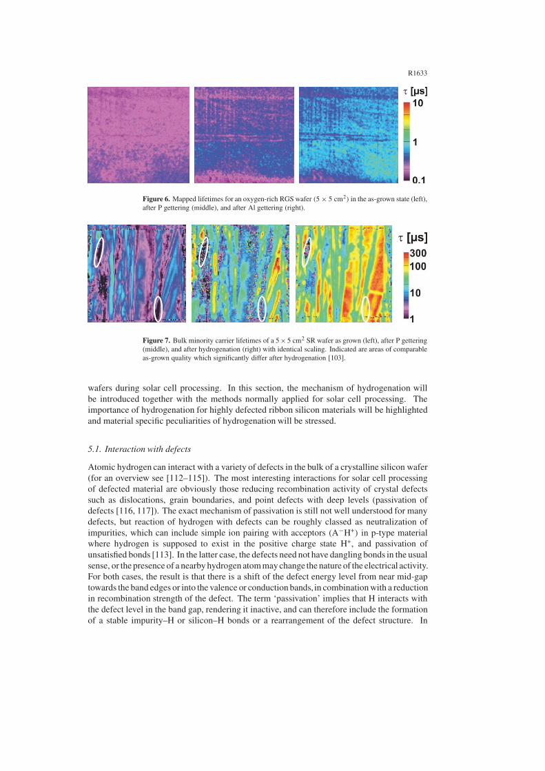
Spatially resolved lifetime measurements additionally allow the determination of standarddeviations [103]. These values are very high due to the inhomogeneity of the material. Theygive a hint as to the amount of information that is lost when performing integral measurementsand again reveal the need for spatially resolved measurement techniques for an accuratecharacterization of ribbon material of inhomogeneous quality (figure 7).
4.3. Gettering in RGS material
The beneficial effect of gettering steps for the formerly oxygen-rich RGS material is limited byinternal gettering processes at oxygen-containing precipitates [109]. This undesired getteringeffect does not remove the metals completely out of the active area (the bulk of the wafer),but can lead to an increased recombination strength of precipitates located at extendeddefects (e.g., dislocations). In figure 6, mapped lifetimes for an oxygen-rich RGS wafer([O] = 3 × 1018 cm−3) in the as-grown state and after different gettering steps are shown.While P gettering raises mean lifetimes slightly from 0.2 to 0.3 μs, Al gettering leads to afurther lifetime increase to 0.5 μs. In contrast, figure 9 (right) shows the same investigationfor an RGS wafer with lower oxygen content (4 × 1017 cm−3). The lower oxygen contentleads to higher as-grown lifetimes, and an increased gettering effect is visible.
From the above findings it can be concluded that the formation of precipitates in thesilicon bulk should be avoided in order to make best use of the gettering step for wafersused in photovoltaics (e.g., by reducing the oxygen content). Interaction between metalsand oxygen leads to stable metal oxides which can hardly be dissolved. The formation of adenuded zone near the wafer surface as observed in gettering processes for wafers used forintegrated circuits [110] cannot be applied for removing metals completely from the active area.Nevertheless, this effect is observed in oxygen-rich highly defected ribbon silicon materials aswell, mainly near grain boundaries, which can act as internal gettering sites and as a sink formetals [111].
5. Hydrogen passivation
It is well known that hydrogen incorporation in crystalline silicon can reduce the recombinationactivity of defects and increase minority carrier lifetimes. Therefore, hydrogenation techniquesplay a major role in improving the material quality of defected areas within multicrystalline
R1633
Figure 6. Mapped lifetimes for an oxygen-rich RGS wafer (5 × 5 cm2) in the as-grown state (left),after P gettering (middle), and after Al gettering (right).
Figure 7. Bulk minority carrier lifetimes of a 5 × 5 cm2 SR wafer as grown (left), after P gettering(middle), and after hydrogenation (right) with identical scaling. Indicated are areas of comparableas-grown quality which significantly differ after hydrogenation [103].
wafers during solar cell processing. In this section, the mechanism of hydrogenation willbe introduced together with the methods normally applied for solar cell processing. Theimportance of hydrogenation for highly defected ribbon silicon materials will be highlightedand material specific peculiarities of hydrogenation will be stressed.
5.1. Interaction with defects
Atomic hydrogen can interact with a variety of defects in the bulk of a crystalline silicon wafer(for an overview see [112–115]). The most interesting interactions for solar cell processingof defected material are obviously those reducing recombination activity of crystal defectssuch as dislocations, grain boundaries, and point defects with deep levels (passivation ofdefects [116, 117]). The exact mechanism of passivation is still not well understood for manydefects, but reaction of hydrogen with defects can be roughly classed as neutralization ofimpurities, which can include simple ion pairing with acceptors (A−H+) in p-type materialwhere hydrogen is supposed to exist in the positive charge state H+, and passivation ofunsatisfied bonds [113]. In the latter case, the defects need not have dangling bonds in the usualsense, or the presence of a nearby hydrogen atom may change the nature of the electrical activity.For both cases, the result is that there is a shift of the defect energy level from near mid-gaptowards the band edges or into the valence or conduction bands, in combination with a reductionin recombination strength of the defect. The term ‘passivation’ implies that H interacts withthe defect level in the band gap, rendering it inactive, and can therefore include the formationof a stable impurity–H or silicon–H bonds or a rearrangement of the defect structure. In
R1634
certain cases, it is therefore more correct to describe the effect of hydrogen on acceptor defectsas neutralization or compensation instead of passivation [113]. Nevertheless, for simplicity,in this work the interaction of H with all defects will be referred to as hydrogenation or Hpassivation.
5.2. Methods for hydrogen incorporation
There are two techniques most commonly used to introduce hydrogen into a silicon wafer:using directed ion beam sources (e.g., Kaufman ion sources [118]) or using plasma reactors.With ion beam sources, hydrogen can be deposited in well known quantities into the siliconwafer. The drawback is the damage caused by the bombardment with high energy atoms.Therefore, it is mainly plasma reactor techniques that are used for hydrogenation of solarcells. Incorporation of H into the silicon bulk can be achieved by direct hydrogen plasmaprocesses [119]. In order to avoid surface damage caused by the plasma being in direct contactwith the wafer, remote plasma techniques have been developed where the H plasma is separatedfrom the sample [120]. This microwave induced remote hydrogen plasma (MIRHP) techniqueis well suited for all laboratory-type studies of hydrogenation in multicrystalline silicon forsolar cells [91, 121–124].
Another plasma based method is the incorporation of hydrogen via a hydrogen-rich SiNx
layer deposited by plasma-enhanced chemical vapour deposition (PECVD [125]). Dependingon the NH3/SiH4 ratio used for the deposition, which also influences the refractive indexand absorption coefficient [126], up to ∼30 at.% can be incorporated into the SiNx [127].The deposited SiNx layer is therefore not of stoichiometric composition. An annealing stepfollowing the SiNx deposition can release atomic hydrogen into the bulk of the wafer [128–130]. Direct experimental evidence of hydrogen being released from the PECVD SiNx layerinto the silicon bulk during the annealing step was found recently for monocrystalline [131] andmulticrystalline silicon material [132]. Besides being a reservoir of hydrogen, the depositedPECVD SiNx layer can simultaneously act as an antireflection coating and can provide excellentsurface passivation [133]. Due to this threefold benefit for solar cell processing [134], PECVDSiNx layers are now state of the art in modern industrial fabrication of multicrystalline solarcells.
5.3. Passivated defects and stability
In addition to the passivation of deep levels, shallow levels can be passivated by H aswell. One example is the passivation of dopants such as B, Al, or P [135]. This isnormally undesirable for solar cell processing as it changes the resistivity of the material.But as the energy needed for reactivation of the ‘defect’ (dopant) calculated based on asimple model [136] is <2 eV in these cases [112], the passivation of shallow levels ordopants is not observed for passivation temperatures in the range of 300–450 ◦C which istypically used for many experiments [137, 138]. Activation energies for other H–defectcomplexes, with the defects being e.g., Au, Pd, Pt, Cu, Ni, Ag, Fe, and grain boundaries(2.2–2.5 eV), as well as dislocations (3.1 eV [139]) causing deep levels in the band gap aresignificantly higher. Therefore, reactivation of these defects takes place at higher temperaturesof about 400 ◦C [112], which is in good agreement with annealing experiments carried outwith hydrogenated solar cells [122, 132, 140, 141]. This makes hydrogen passivation ofrecombination active deep level defects in defected solar cell material quite thermally stable.
5.4. Hydrogenation of EFG and SR materials
The benefit of hydrogenation in EFG material was manifested in early studies by areduction of the recombination activity of dislocations and grain boundaries after ion

R1635
implantation [116, 142]. Other, more recent studies revealed the effect of hydrogenation on bulklifetimes for EFG and SR materials by using remote plasma techniques [102, 103, 105, 106]or passivation from PECVD SiNx layers [100, 104]. It was found that hydrogenationusing MIRHP causes a larger increase in bulk lifetimes than observed for Al or P getteringsteps. Whereas gettering techniques improve mainly good quality areas of the as-grownwafer, hydrogen treatment can improve areas of all qualities significantly. Nevertheless,the achievable final lifetime after hydrogenation is not a function of lifetime in the as-grown state alone [102, 103, 105, 106]. This clearly demonstrates the complex situationof inhomogeneous defect distribution in ribbon silicon. The efficiency of hydrogenation isstrongly dependent on the underlying defects. Figure 7 shows lifetimes of a SR wafer in theas-grown state, after Al gettering, and after MIRHP hydrogenation. Indicated are areas ofcomparable starting lifetimes, resulting in areas of significantly different lifetimes after thegettering and hydrogenation step. As dislocations contaminated with precipitates seem toplay the major role in recombination activity, an explanation for the different behaviours isthe change in chemical composition of these precipitates. Dependent on the nature of theprecipitates [66, 67], hydrogenation is more or less effective in reducing the recombinationstrength.
It can be shown that hydrogenation is stable under illumination, provided that a getteringstep precedes the hydrogenation step [102]. Without this gettering step, lifetimes tend todecrease slightly upon illumination. The reason for this instability is unclear, but it couldinvolve activation of transition metal based defects such as Fe–B or Cr–B ones.
Furthermore, an increased passivation effect has been observed when Al is present atthe wafer surface during hydrogenation of a PECVD SiNx layer [101, 134, 143]. Thissynergetic effect, which leads to larger increases in carrier lifetimes than separate getteringand hydrogenation steps, is possibly explained by increased vacancy formation due to the Alalloying process and enhanced hydrogen diffusivity [143]. This theory could not be proven,as experiments to determine vacancy concentrations before and after Al alloying did not showan increase in SiV [144].
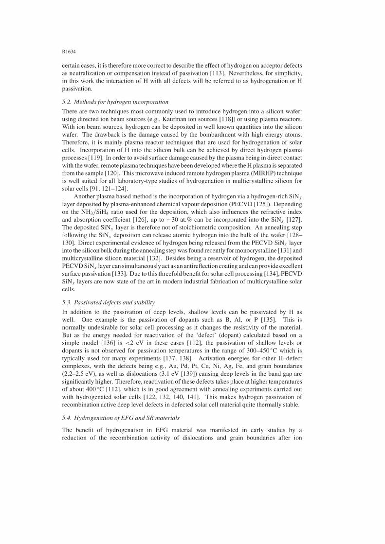
The effect of gettering and hydrogenation steps on lifetimes in EFG and SR materials isshown again in figure 8. Data have been obtained on wafers fabricated according to processingsequences presented in more detail elsewhere [102]. Wafer 1 shows slight instability of thehydrogenationafter illumination without a preceding gettering step, especially for areas of highlifetimes. Wafers 2 and 3 indicate stability of hydrogenation if a P (wafer 2) or Al getteringstep (wafer 3) precedes the hydrogenation. Additionally, the effect of higher lifetimes resultingfrom a combination of gettering and hydrogenation can be seen. Combination of P and Algettering (cogettering) seems to be more effective than P or Al gettering alone, but does notlead to significantly higher lifetimes upon hydrogenation (wafer 4).
Retention of hydrogen at the defects is important for maintaining the passivation properties.For temperatures of >400 ◦C reactivation of recombination activity can be observed, due tothermal activation. Therefore, cooling rates after H passivation are important. Hydrogenationfrom PECVD SiNx layers with annealing temperatures in the range of 700–850 ◦C can besignificantly affected by cooling-down ramps. Experiments using rapid thermal processing(RTP) in combination with PECVD SiNx layers revealed that higher lifetimes can be achievedby using fast cool-down ramps [145, 146].
5.5. Hydrogenation in RGS material
Hydrogen passivation of defects in RGS material is also important; as-grown material lifetimesare lower than those for EFG and SR materials (table 2). For material with high interstitial
R1636
1 10 100
1 10 100 1 10 100
as-grown P-gettered
Wafer 2
freq
uenc
y [a
.u.]
hydrogenated illuminated
Wafer 1
Wafer 4
Al-gettered
Wafer 3
ττττ [μs]
P-Al-cogettered
freq
uenc
y [a
. u.]
ττττ [μs]
Figure 8. Histograms of μPCD lifetime mappings carried out on four EFG wafers (5 × 5 cm2) afterdifferent processing steps. Wafers 2 and 3 are adjacent and reveal similar crystal grain structures;the same holds true for wafers 1 and 4. More details are given elsewhere [102].
oxygen content, the formation of new donors was found to increase the density of bulk trapstates drastically [79], further reducing material quality. A hydrogenation step carried outafterwards was shown to cause the material quality to recover, proving that new donors canbe effectively passivated by hydrogen [79]. Nevertheless, the high oxygen content seemsto hinder the effectiveness of hydrogenation. D profiles obtained for RGS material onlydiffering in interstitial oxygen concentration showed a reduced diffusion for higher oxygencontents [138]. This effect was also observed for other materials [91] and can be explainedby oxygen lowering the propensity for generation of vacancies [147]. Alternative modelsare presented in the next paragraph. Whereas for low oxygen materials such as EFG ones,hydrogen diffuses through the whole wafer within ∼30 min at 350 ◦C, this takes several hoursin the case of oxygen-rich RGS material [91].
Lifetimes for oxygen-rich materials have been limited to values of <1 μs, even afteroptimized hydrogenation steps [86]. A lowering of the overall oxygen content to valuesof ∼5 × 1017 cm−3 in recently obtained RGS material [58] led to lifetimes of ∼3 μs aftergettering and hydrogenation. A positive side effect is that hydrogenation time in this case canbe significantly shorter, as diffusion is faster.
5.6. Diffusion of H in defected silicon
The diffusion kinetics of hydrogen plays an important role in defected crystalline siliconmaterial. Van Wieringen and Warmoltz [148] determined diffusivities in monocrystalline

R1637
1 10
τ [μs]1 10
τ [μs]
freq
uen
cy [
a. u
.]
freq
uen
cy [
a. u
.]RGS 63_5 (high O)
as-grown after P-gettering after Al-gettering after MIRHP 24h 450°C
RGS 257_10A (low O) as-grown after Al-gettering after MIRHP 2h 350°C
Figure 9. Histograms of μPCD lifetime mappings carried out for two RGS wafers (5 × 5 cm2)
with high (3 × 1018 cm−3, left) and reduced oxygen concentration (4 × 1017 cm−3, right) afterdifferent processing steps. While lifetime enhancement is limited for the high oxygen wafer dueto internal gettering and trapping of hydrogen, higher lifetimes can be reached for lower oxygenconcentrations.
Table 3. Concentrations of SiV and interstitial oxygen in various crystalline ribbon siliconmaterials (from [144, 151]).
As-grown [Oi] [Oi] after POCl3 [SiV] after POCl3Material (cm−3) diffusion (cm−3) diffusion (cm−3)
EFG <1017 <1017 10 × 1012
SR <1017 <1017 ∼10 × 1012
RGS, high [O] 29 × 1017 4 × 10¹⁷ <1 × 10¹²
RGS, low [O] 4 × 10¹⁷ 3 × 10¹⁷ 20–30 × 1012
silicon at high temperatures. Extrapolation to lower temperatures from these data leads todiffusion constants for hydrogen of 1.1 × 10⁻⁶ cm2 s−1 at 350 ◦C and 3.8 × 10⁻⁵ cm2 s−1
at 750 ◦C. From these data we should expect diffusion of hydrogen through the entirewafer within <30 min at 350 ◦C or <20 s at 750 ◦C. While this seems to be the case forEFG and SR materials [91, 149], hydrogen diffusivity in oxygen-rich materials is sloweddown [91, 138, 150]. One explanation could be the reduced vacancy concentration inthe presence of a high oxygen content [132, 151] (table 3). According to this model,vacancies can dissociate immobile hydrogen molecules to atomic hydrogen [152, 153]. A lowvacancy concentration would therefore result in increased molecule formation reducing theatomic hydrogen content available for diffusion and passivation. The formation of immobilehydrogen molecules [112, 154] might therefore be hindered in materials with higher vacancyconcentration such as EFG and SR materials, resulting in a faster diffusion.
A further model proposed by Sopori et al [147] favours the formation of a H–SiV complexand its rapid diffusion through the lattice [155, 156].
Another explanation of reduced diffusivity in oxygen-rich materials is a direct interactionbetween H and O, resulting in trapping of hydrogen. Interaction between H and interstitialoxygen is known to enhance the diffusivity of oxygen and increase the formation of thermaldonors [157, 158]. A proposed trapping of hydrogen near interstitial oxygen [158] couldtherefore explain the observed low diffusivities of hydrogen in oxygen-rich material.
On the other hand, it is known that hydrogen can passivate thermal donors [159] aswell as new donors [79] indicating a direct coupling with the concentration of these defects.

R1638
High oxygen concentrations should thus lead to trapping of hydrogen, especially when thetrap concentration is large as compared to the hydrogen concentration. Trapping due to high(∼1018 cm−3) oxygen concentrations can therefore explain the prolonged times needed forhydrogen diffusion through the whole wafer, either by trapping near interstitial oxygen or atthermal or new donors. In this model [132] the diffusivity of hydrogen is dependent on theamount of oxygen precipitates (e.g. new donors) present and their surface area, as the interaction(trapping) between hydrogen and precipitate is assumed to take place via its surface. In this waythe observed variations in hydrogen diffusivity for materials differing in oxygen concentrationcan be explained if the thermal history is taken into account, which determines the size andamount of the precipitates [132].
6. Ribbon silicon solar cells
Fabrication of solar cells using ribbon silicon wafers has to be adapted to the material needs inorder to reach satisfactory conversion efficiencies. As for all multicrystalline silicon wafers,material quality should be improved during cell processing to cope with the defect structurepresent in the as-grown material. This is in contrast to the case for monocrystalline floatzone material, where the main task is to maintain the high as-grown material quality duringprocessing steps. It was shown in the previous sections that ribbon material quality can besubstantially improved by gettering and hydrogenation. The implementation of these stepsinto the solar cell process is therefore crucial, as the efficiency obtainable for solar cells froma given material is important for cost-effectiveness.
6.1. Laboratory-type and industrial-type processing
When considering efficiencies, two types of cell process have to be distinguished, namelylaboratory-type and industrial-type processing. Laboratory-type processing normally resultsin small area cells (∼4 cm2) and makes use of processing steps regardless of the cost perwafer. The purpose is usually to determine the material potential or to fundamentally developand test new processing sequences in a very controlled way. Contacts are normally formedby evaporation techniques to achieve good contact resistance and to enable a good spectralresponse in the short wavelength region as high emitter sheet resistances can be used. Thefront metal grid is usually defined by a photolithography step to minimize grid shadowinglosses, which are in the region of 4%.
On the other hand, industrial-type processing simulates the efficiency obtainable in largescale production. Therefore, significantly larger cell areas, normally �100 cm2, are used,which is closer to cell formats commercially used in industry. Processing steps are restrictedby consideration of costs which means that e.g. for front contact formation, generally thickfilm metallization is applied (the only other alternative currently used in industry in significantvolumes is the buried grid technology [160]). Thick film metallization via deposition of metal-containing pastes and subsequent firing to obtain ohmic contacts results in higher shadowinglosses (∼7%) and currently does not allow as high emitter sheet resistivities as are used forlaboratory-type evaporation techniques without selective emitter structures. Efficiencies aretherefore significantly lower for industrial-type processing. Another reason for the lowerrecord values of industrial-type cells is the presence of inhomogeneities in the material quality,especially when variations are on the same scale as the cell size used for laboratory-typeprocessing.
Examples of two typical processes are shown schematically in figure 10. In both processes,gettering and hydrogenation steps are implemented. P gettering takes place during P diffusion.For laboratory-type processing, POCl3 is usually used as the dopant source in an open tube

R1639
furnace resulting in an emitter on both front and rear sides. For industrial-type processes,an alternative to using POCl3 is using one-sided diffusion, e.g. by using a spray-on or spin-on dopant and diffusion in a belt furnace. Gettering action might be reduced in the lattercase as only one surface acts as a sink for metal impurities [161, 162]. Al gettering in alaboratory-type process can be obtained by evaporation of Al (∼2 μm) followed by alloyingat temperatures above the eutectic point of Al/Si, normally in the range of 800 ◦C for ∼30 min.This step simultaneously serves to overcompensate the parasitic back emitter and to form aBSF to hinder recombination of minority charge carriers at the back of the cell. Al getteringfor industrial-type processes is limited to the firing step for contact formation.
Hydrogenation can be applied via remote plasma techniques on finished cell structuresfor laboratory-type processing. In this way, the beneficial effect can be quantified directlyon the cell level. The only limitation is that the temperature load is limited due to possiblein-diffusion of metals from the front metallization into the emitter, which results in shuntformation. This limits hydrogenation to temperatures of <450 ◦C and durations of ∼1 h(dependent on temperature [163]). This restriction can be overcome if hydrogenation is appliedprior to contact formation [164]. Hydrogenation for industrial-type processing is generallycarried out using hydrogen-rich PECVD SiNx layers. The hydrogen stored in the SiNx isreleased into the bulk during the firing step, which has to be designed properly in order to alsoprovide both a good contact and BSF formation.
An evaporated double-layer antireflective coating (DARC; e.g. ZnS/MgF2) reducesreflection losses in the case of laboratory-type processing,whereas for industrial-type processesthe PECVD SiN acts as a single-layer ARC.
6.2. EFG and SR solar cells
Both EFG and SR wafers are fabricated commercially and solar cells have been processed ona large scale, industrial basis since 1994 (EFG material) and 2001 (SR material). For EFGin particular, the research was intensive and publication of solar cell results with efficienciesexceeding 14% using a laboratory-type process dates back to 1983 [142]. Further progressin laboratory-type efficiency improvement was comparatively slow for EFG material until themid-1990s, as can be seen from figure 11. From this time on, SR and EFG material recordefficiencies have developed in parallel, again demonstrating their comparable material quality.
As material quality is inhomogeneous even after gettering and hydrogenation (see figure 7),solar cell results are affected by both good and bad areas. Cell performance in areas of lowdiffusion length is limited due to recombination in the bulk, whereas rear surface recombination,Sb, can limit carrier collection in good quality areas.
The Al gettering step in the laboratory-type process shown in figure 10 with evaporation ofAl (thickness 1–2 μm) is effective in removing metal atoms, but results only in minor values forSb because the BSF thickness is <1 μm and the peak concentration of Al in the BSF is around5×1018 cm−3 [166]. To cope with this restriction, thicker BSFs obtained using screen-printingand firing of Al paste have been implemented in laboratory-type processing [108] resulting inBSF thicknesses of 8–10 μm. In this way, values for Sb in the range 300–600 cm s−1 can beobtained for material with bulk resistivities of 3 � cm [166]. Areas with high Ldiff benefitespecially from the lower back surface recombination (figure 12), and a significant increase inefficiency for laboratory-type processes was obtained [108].
Areas of lower material quality are of special interest, as these regions normally limit cellefficiency. Lower quality areas can be improved mainly by hydrogenation[102, 105]; thereforebulk defect passivation kinetics has been studied intensively. It was shown that retention ofhydrogen at the defect sites can only be achieved for temperatures of <400 ◦C if no cappinglayer is present [140, 167]. Similar results have been obtained for cells with a SiNx layer on

R1640
Lab-type process Industrial-type process
defect etchingdefect etching / texture
P-diffusion (50Ω/sq)
P-glass etching
PECVD SiN deposition
edge isolation (plasma)
thick film front contact
thick film back contact
co-firing
P-diffusion (90Ω/sq)
P-glass etching
thermal oxidation
Al-gettering
photolithography
Ti/Pd/Ag front contact
Al rear contact
electroplating
cell isolation (dicing)
hydrogenation
DARC deposition
Figure 10. Typical solar cell fabrication sequences used for laboratory-type processing (left) andindustrial-type processing (right).
1982198419861988 19901992 19941996 19982000 2002200412
13
14
15
16
17
18
19
EFG SR
lab
-typ
e ηη ηη
[%]
1982 198419861988 1990 19921994 1996 199820002002 200412
13
14
15
16
17
18
19
EFG SR
ind
ust
rial
-typ
e ηη ηη
[%]
Figure 11. Progress in record efficiencies for EFG and SR solar cells using laboratory-type (left)and industrial-type processing (right). Some of the data are from [165].
top of the emitter [100, 141]. To ensure retention of hydrogen at the defect sites subsequent tohydrogenation, temperature ramps are critical. This is especially important for hydrogenationvia a PECVD SiNx layer, as the optimum temperature for hydrogenation is between 650and 800 ◦C, depending on the frequency used for plasma excitation during SiNx depositionand whether there is Al present on the back [146, 168]. At these elevated temperatures,hydrogen can be released from the defect site and the recombination strength of the defectcan be restored. Studies using rapid thermal processing (RTP) demonstrate that retention ofhydrogen is a function of annealing time and cooling rates [104, 149, 165, 169]. Optimumpassivation was achieved by annealing at 750 ◦C for just 1 s (excluding the time for rampingup and down). It is interesting to compare this result with the hydrogen diffusivity data of vanWieringen and Warmoltz [148] on monocrystalline silicon presented above. Extrapolationof their data reveals that a few seconds of annealing at 750 ◦C should be sufficient for the
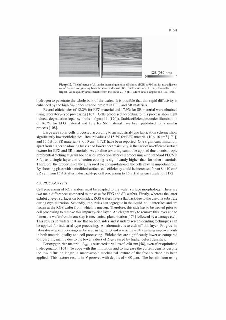
R1641
Figure 12. The influence of Sb on the internal quantum efficiency (IQE) at 980 nm for two adjacent4 cm2 SR cells originating from the same wafer with BSF thicknesses of <1 μm (left) and 8–10 μm(right). Good quality areas benefit from the lower Sb (right). More details appear in [108, 166].
hydrogen to penetrate the whole bulk of the wafer. It is possible that this rapid diffusivity isenhanced by the high SiV concentration present in EFG and SR materials.
Record efficiencies of 18.2% for EFG material and 17.9% for SR material were obtainedusing laboratory-type processing [167]. Cells processed according to this process show lightinduced degradation (open symbols in figure 11, [170]). Stable efficiencies under illuminationof 16.7% for EFG material and 17.7 for SR material have been published for a similarprocess [108].
Large area solar cells processed according to an industrial-type fabrication scheme showsignificantly lower efficiencies. Record values of 15.3% for EFG material (10×10 cm2 [171])and 15.6% for SR material (8 × 10 cm2 [172]) have been reported. One significant limitation,apart from higher shadowing losses and lower sheet resistivity, is the lack of an efficient surfacetexture for EFG and SR materials. As alkaline texturing cannot be applied due to anisotropicpreferential etching at grain boundaries, reflection after cell processing with standard PECVDSiNx as a single-layer antireflection coating is significantly higher than for other materials.Therefore, the properties of the glass used for encapsulation of the cells play an important role.By choosing glass with a modified surface, cell efficiency could be increased for an 8×10 cm2
SR cell from 15.4% after industrial-type cell processing to 15.8% after encapsulation [172].
6.3. RGS solar cells
Cell processing of RGS wafers must be adapted to the wafer surface morphology. There aretwo main differences compared to the case for EFG and SR wafers. Firstly, whereas the latterexhibit uneven surfaces on both sides, RGS wafers have a flat back due to the use of a substrateduring crystallization. Secondly, impurities can segregate in the liquid–solid interface and arefrozen at the RGS wafer front, which is uneven. Therefore, this side has to be treated prior tocell processing to remove this impurity-rich layer. An elegant way to remove this layer and toflatten the wafer front in one step is mechanical planarization [173] followed by a damage etch.This results in wafers that are flat on both sides and standard screen-printing techniques canbe applied for industrial-type processing. An alternative is to etch off this layer. Progress inlaboratory-type processing can be seen in figure 13 and was achieved by making improvementsin both material quality and cell processing. Efficiencies are significantly lower as comparedto figure 11, mainly due to the lower values of Ldiff caused by higher defect densities.
For oxygen-rich material, Ldiff is restricted to values of <50 μm [58], even after optimizedhydrogenation [164]. To cope with this limitation and to increase the current density despitethe low diffusion length, a macroscopic mechanical texture of the front surface has beenapplied. This texture results in V-grooves with depths of ∼60 μm. The benefit from using
R1642
this procedure for the RGS solar cell is threefold: reflection losses are reduced, carriersare generated closer to the wafer surface due to the inclined penetration of the light, andthe collection probability of generated charge carriers is enhanced due the reduced distancebetween the site of generation and the emitter, which follows the V-grooved surface [174].The beneficial effect of the grooving is dependent on Ldiff and in the range of 6%rel–8%rel
efficiency increase for Ldiff < 100 μm.As described earlier, hydrogenation in oxygen-rich RGS material is reduced compared to
that in EFG and SR materials, and even several hours of passivation at 450 ◦C are not sufficientfor the hydrogen to penetrate the whole wafer [132]. Therefore remote plasma passivation hasto be applied prior to metallization, in contrast to the case in the processing scheme used forEFG and SR wafers, shown in figure 10. Optimization of this step as regards temperature andduration in combination with a V-grooved surface texture led to efficiencies of 12.5% [164]and more recently 13.2% on 2 × 2 cm2 cells [175] in oxygen-rich material.
For practical reasons, RGS wafers were cut down from 8.6×13 to 5×5 cm2 for industrial-type processing. Using this wafer format, efficiencies of 10.5% have been reached using RGSmaterial with a high oxygen content [58]. This process involved a remote plasma passivationstep in addition to hydrogenation via PECVD SiNx and firing. Reducing the oxygen contentin RGS wafers results in significantly higher charge carrier lifetimes and therefore higherdiffusion lengths, as was shown in the previous sections. As a consequence, short circuitcurrent densities on untextured wafers can be enhanced from ∼24 to >28 mA cm−2 and opencircuit voltages increase from 565 to >580 mV in solar cells fabricated from this material,resulting in efficiencies in the 12–13% region [175].
A clear efficiency increase can also be expected for the low oxygen material in laboratory-type processing.
6.4. Summary
Solar cells made from ribbon silicon wafers are more cost-effective when efficiencies are inthe same range as for cells from costlier wafers originating from ingots. Record efficienciesfor EFG and SR cells in the range of 17%–18% are comparable to those for the best cellsfabricated from multicrystalline wafers from ingots when laboratory-type processes of thesame complexity are used. The same is true for industrial-type processing, with recordefficiencies between 15% and 16% and mean values between 14% and 15% for EFG solarcells in production [171]. From these data, it can be concluded that solar cells from EFG orSR wafers have a significant advantage as regards cost per Wp, provided that a comparableyield is achieved.
RGS wafers have the advantage of a more cost-effective fabrication due to the highproduction speed. The expectation is that, even if the efficiency is somewhat lower, theintroduction of RGS material would further reduce the costs per Wp of PV modules. Theimprovements in wafer quality and the increased understanding of the interaction betweendefects and solar cell processing makes it very likely that higher efficiency values will bereached soon. The target is the 14% region with industrial-type processes in the near future, aprospect that seems to be promising if the dynamic efficiency development shown in figure 13is considered.
In addition to the cost-effectiveness of silicon ribbons, the energy payback time (i.e. thetime needed to produce the amount of energy that was consumed during the manufacturingof a solar system) is drastically reduced. In a recent life-cycle analysis of crystalline siliconwafer based PV systems it was demonstrated that the energy payback times can be reducedfrom 4.3 years (based on cut multicrystalline wafers) to 2.0 years by the use of RGS ribbonsfor systems in central Europe [176].
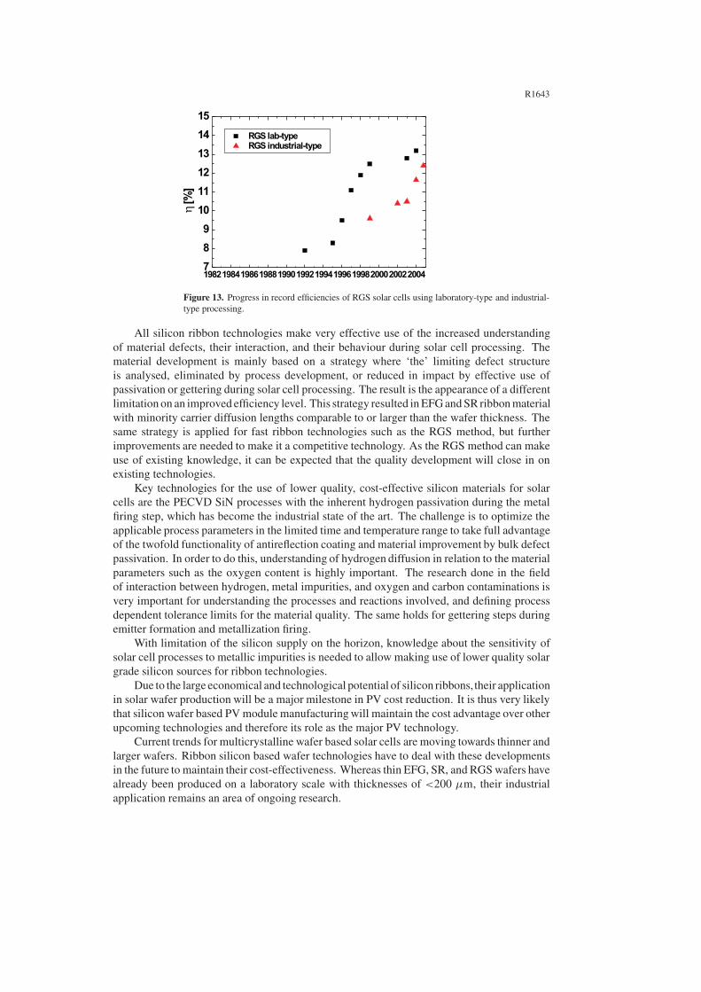
R1643
Figure 13. Progress in record efficiencies of RGS solar cells using laboratory-type and industrial-type processing.
All silicon ribbon technologies make very effective use of the increased understandingof material defects, their interaction, and their behaviour during solar cell processing. Thematerial development is mainly based on a strategy where ‘the’ limiting defect structureis analysed, eliminated by process development, or reduced in impact by effective use ofpassivation or gettering during solar cell processing. The result is the appearance of a differentlimitation on an improved efficiency level. This strategy resulted in EFG and SR ribbon materialwith minority carrier diffusion lengths comparable to or larger than the wafer thickness. Thesame strategy is applied for fast ribbon technologies such as the RGS method, but furtherimprovements are needed to make it a competitive technology. As the RGS method can makeuse of existing knowledge, it can be expected that the quality development will close in onexisting technologies.
Key technologies for the use of lower quality, cost-effective silicon materials for solarcells are the PECVD SiN processes with the inherent hydrogen passivation during the metalfiring step, which has become the industrial state of the art. The challenge is to optimize theapplicable process parameters in the limited time and temperature range to take full advantageof the twofold functionality of antireflection coating and material improvement by bulk defectpassivation. In order to do this, understanding of hydrogen diffusion in relation to the materialparameters such as the oxygen content is highly important. The research done in the fieldof interaction between hydrogen, metal impurities, and oxygen and carbon contaminations isvery important for understanding the processes and reactions involved, and defining processdependent tolerance limits for the material quality. The same holds for gettering steps duringemitter formation and metallization firing.
With limitation of the silicon supply on the horizon, knowledge about the sensitivity ofsolar cell processes to metallic impurities is needed to allow making use of lower quality solargrade silicon sources for ribbon technologies.
Due to the large economical and technological potential of silicon ribbons, their applicationin solar wafer production will be a major milestone in PV cost reduction. It is thus very likelythat silicon wafer based PV module manufacturing will maintain the cost advantage over otherupcoming technologies and therefore its role as the major PV technology.
Current trends for multicrystalline wafer based solar cells are moving towards thinner andlarger wafers. Ribbon silicon based wafer technologies have to deal with these developmentsin the future to maintain their cost-effectiveness. Whereas thin EFG, SR, and RGS wafers havealready been produced on a laboratory scale with thicknesses of <200 μm, their industrialapplication remains an area of ongoing research.

R1644
Producing larger area square wafers should not be a general problem for the RGStechnology, due to the local growth supported by a rigid substrate, whereas increasing thewafer width might be more problematic in EFG and SR technologies. Nevertheless, the cellarea for EFG and SR wafers can be easily increased by using rectangular wafers with constantwidth and increased length.
References
[1] Schmela M 2004 Photon Int. 3 46[2] SEMI M1-0704, Specifications for Polished Mono-Crystalline Silicon Wafers, Semiconductor Equipment and
Materials International (www.semi.org)[3] SEMI M6-1000, Specifications for Silicon Wafers for Use as Photovoltaic Solar Cells, Semiconductor
Equipment and Materials International (www.semi.org)[4] Phillips M J 1986 Summary of the Flat-Plate Solar Array Project Documentation: Abstracts of Published
Documents, 1975 to 1986 DOE/JPL-1012-76[5] Koch W, Hassler C, Hofs H-U, Muller A and Schwirtlich I A 1997 Solid State Phenom. 57/58 401[6] Ciszek T F 1996 High Purity Silicon IV ed C L Claeys, P Rai-Choudhury, P Stallhofer and
J E Maurtis (Pennington, MN: The Electrochemical Society) p 76[7] Sarti D and Einhaus R 2002 Sol. Energy Mater. Sol. Cells 72 27[8] de Vos A 1992 Endoreversible Thermodynamics of Solar Energy Conversion (Oxford: Oxford University
Press)[9] Zhao J, Wang A and Green M A 1999 Progr. Photovolt. Res. Appl. 7 471
[10] Shockley W and Read W T 1952 Phys. Rev. 87 835[11] Hall R N 1952 Phys. Rev. 87 387[12] Fally J, Fabre E and Chabot B 1987 Rev. Phys. Appl. 22 529[13] Davis J R, Rohatgi A, Hopkins R H, Blais P D, Rai-Choudhury P, McCormic J R and Mollenkopf H C 1980
IEEE Trans. Electron Devices 27 677[14] Dermatis S N and Faust J W 1963 IEEE Trans. Commun. Electron. 82 94[15] Boatman J and Goundry P 1967 Electrochem. Technol. 5 98[16] Ciszek T F 1972 Mater. Res. Bull. 7 731[17] Koyanagi T 1976 Proc. 12th IEEE PVSC (Baton Rouge) (US: IEEE, Library of Congress) p 627[18] Belouet C 1987 J. Cryst. Growth 82 110[19] Lesk I A, Baghadadi A, Gurtler R W, Ellis R J, Wise J A and Coleman M G 1976 Proc. 12th IEEE PVSC
(Baton Rouge) (US: IEEE, Library of Congress) p 173[20] Heaps J D, Maciolek R B, Zook J D and Scott M W 1976 Proc. 12th IEEE PVSC (Baton Rouge) (US: IEEE,
Library of Congress) p 147[21] Ciszek T F and Schwuttke G H 1977 J. Cryst. Growth 42 483[22] Ciszek T F and Hurd J L 1980 Proc. 14th IEEE PVSC (San Diego) (US: IEEE, Library of Congress) p 397[23] Kim K M, Berkman S, Duffy M T, Bell A E, Temple H E and Cullen G W 1977 Silicon Sheet Growth by the
Inverted Stepanov Technique DOE/JPL-954465[24] Tsuya N, Arai K I, Takeuchi T, Ohmor K, Ojima T and Kuroiwa A 1980 J. Electron. Mater. 9 111[25] Ciszek T F, Hurd J L and Schietzelt M 1982 J. Electrochem. Soc. 129 2838[26] Bates H E and Jewett D M 1981 Proc. 15th IEEE PVSC (Kissimmee) (US: IEEE, Library of Congress) p 255[27] Grabmaier J G and Falckenberg R 1990 J. Cryst. Growth 104 191[28] Beck A, Geissler J and Helmreich D 1987 J. Cryst. Growth 82 127[29] Eyer A, Schillinger N, Reis I and Rauber A 1990 J. Cryst. Growth 104 119[30] Lange H and Schwirtlich I 1990 J. Cryst. Growth 104 108[31] Suzuki M, Hide I, Yokoyama T, Matsuyama T, Hatanaka Y and Maeda Y 1990 J. Cryst. Growth 104 102[32] Maeda Y, Yokoyama T, Hide I, Matsuyama T and Sawaya K 1986 J. Electrochem. Soc.: Solid State Sci.
Technol. 133 440[33] Komatsu Y, Koide N, Yang M-J, Nakano T, Nagano Y, Igarashi K, Yoshida K, Yano K, Hayakawa T,
Taniguchi H, Shimizu M and Takiguchi H 2003 Sol. Energy Mater. Sol. Cells 74 513[34] Konagai M 2002 Proc. 29th IEEE PVSC (New Orleans) (US: IEEE, Library of Congress) p 38[35] Ciszek T F 1984 J. Cryst. Growth 66 655[36] Wald F W 1981 Crystals: Growth, Properties, and Applications vol 5, ed J Grabmaier (Berlin: Springer) p 147[37] Sachs W M, Ely D and Serdy J 1987 J. Cryst. Growth 82 117

R1645
[38] Culik J S, Faller F, Goncharovsky I S, Rand J A and Barnett A M 2001 Proc. 17th EC PVSEC (Munich)(Munich: WIP) p 1347
[39] Ciszek T F 1976 J. Appl. Phys. 47 440[40] Kalejs J P 1993 J. Cryst. Growth 128 298[41] Wallace R J, Hanoka J I, Narasimha S, Kamra S and Rohatgi A 1997 Proc. 26th IEEE PVSC (Anaheim) (US:
IEEE, Library of Congress) p 99[42] Cho S H and Sunderland J E 1969 J. Heat Transfer 91c 421[43] Rao C V H N, Cretella M C, Wald F V and Ravi K V 1980 J. Cryst. Growth 50 311[44] Garone L C, Hari Rao C V, Morrison A D, Surek T and Ravi K V 1976 Appl. Phys. Lett. 29 511[45] Briglio A, Dumas K, Leipold M and Morrison A 1986 Flat Plate Solar Array Project: Volume III Silicon
Sheets and Ribbons DOE/JPL 1012-125[46] Hull R 1999 Properties of Crystalline Silicon (London: Inspec)[47] Janoch R E, Anselmo A P, Wallace R L, Martz J, Lord B E and Hanoka J I 2000 Proc. 28th IEEE PVSC
(Anchorage) (US: IEEE, Library of Congress) p 1403[48] Hirata H and Hoshikawa K 1980 Japan. J. Appl. Phys. 19 1573[49] Schei A, Tuset J and Tveit H 1998 Production of High Silicon Alloys (Trondheim: Tapir Forlag)[50] Li J-G and Hausner H 1995 Scr. Metall. Mater. 32 377[51] Li J-G and Hausner H 1996 J. Am. Ceram. Soc. 97 873[52] Deike R and Schwerdtfeger K 1995 J. Electrochem. Soc. 142 609[53] Yanabe K, Akasaka M, Takeuchi M, Watanabe M, Narushima T and Iguchi Y 1997 Mater. Trans. JIM 38 990[54] Kalejs J P 1987 Silicon Processing for Photovoltaics II ed C P Khattak and K V Ravi (Amsterdam: Elsevier)
p 185[55] Bhihe C K, Mataga P A, Hutchinson J W, Rajendran S and Kalejs J P 1994 J. Cryst. Growth 137 86[56] Wallace L W, Sachs E and Hanoka J I 2003 Proc. 3rd WCPEC (Osaka) (Japan: WCPEC-3 Organising
Committee, Arisumi Printing Inc.) p 1297[57] Sachs E, Harvey D, Janoch R, Anselmo A, Miller D and Hanoka J I 2004 Proc. 19th EC PVSEC (Paris) at
press[58] Hahn G, Seren S, Sontag D, Schonecker A, Goris M, Laas L and Gutjahr A 2003 Proc. 3rd WCPEC (Osaka)
(Japan: WCPEC-3 Organising Committee, Arisumi Printing Inc.) p 1285[59] Hassler C, Hoefs H-U, Koch W, Stollwerk G, Mueller A, Karg D and Pensl G 2000 Mater. Sci. Eng. B 71 39[60] Kalejs J P 2004 Solid State Phenom. 95/96 159[61] Chalmers B 1984 J. Cryst. Growth 70 3[62] Koshka Y, Ostapenko S, Tarasov I, McHugo S and Kalejs J P 1999 Appl. Phys. Lett. 74 1555[63] Ostapenko S, Tarasov I, Kalejs J P, Hassler C and Reisner E-U 2000 Semicond. Sci. Technol. 15 840[64] Moller H J, Funke C, Lawerenz A, Riedel S and Werner M 2002 Sol. Energy Mater. Sol. Cells 72 403[65] Werner M, Scheerschmidt K, Pippel E, Funke C and Moller H J 2004 Phys. Conf. Ser. 180 65[66] Knobloch K, Kittler M and Seifert W 2003 J. Appl. Phys. 93 1069[67] Kittler M, Seifert W, Arguirov T, Tarasov I and Ostapenko S 2002 Sol. Energy Mater. Sol. Cells 72 465[68] Bailey J, McHugo S, Hieslmair H and Weber E W 1996 J. Electron. Mater. 25 1417[69] Bailey J and Weber E R 1993 Phys. Status Solidi a 137 515[70] Pivac B, Amiotti M, Borghesi A, Sassella A and Kalejs J 1992 J. Appl. Phys. 71 3785[71] Kalejs J P, Ladd L A and Gosele U 1984 Appl. Phys. Lett. 45 268[72] Kalejs J P, Jastrzebski L, Lagowski L, Henley W, Schielein D, Balster S G and Schroder D K 1994 Proc. 12th
EC PVSEC (Amsterdam) (Bedford: HS Stephens) p 52[73] Kalejs J P, Bathey B R, Borenstein J T and Stormont R W 1993 Proc. 23rd IEEE PVSC (Louisville) (US: IEEE,
Library of Congress) p 184[74] Mishra K 1996 Appl. Phys. Lett. 68 3281[75] Klettke O, Karg D, Pensl G, Schulz M, Hahn G and Lauinger T 2001 Technical Digest 12th PVSEC (Jeju)
(Seoul: International PVSEC-12) p 617[76] Macdonald D, Cuevas A and Wong-Leung J 2001 J. Appl. Phys. 89 7932[77] Cazcarra V and Zunino P 1980 J. Appl. Phys. 51 4206[78] Kamiura Y, Hashimoto F and Yoneta M 1991 Phys. Status Solidi a 123 357[79] Karg D, Voigt A, Krinke J, Hassler C, Hoefs H-U, Pensl G, Schulz M and Strunk H P 1999 Solid State Phenom.
67/68 33[80] Hassler C, Hoefs H-U and Thurm S 2000 Proc. 16th EC
PVSEC (Glasgow) (London: James & James) p 1352[81] Gottschalk H 2000 Phys. Status Solidi b 222 353[82] Lu J, Rozgonyi G, Schonecker A and Gutjahr A 2004 Appl. Phys. Lett. submitted
R1646
[83] McHugo S, Thompson A C, Mohammed A, Lamble G, Perichaud I, Martinuzzi S, Werner M, Rinio M, Koch W,Hoefs H-U and Hassler C 2001 J. Appl. Phys. 89 4282
[84] Buonassisi T, Vyvenko O F, Istratov A A, Weber E R, Hahn G, Sontag D, Rakotoniaina J P, Breitenstein O,Isenberg J and Schindler R 2004 J. Appl. Phys. 95 1556
[85] Sontag D, Hahn G, Geiger P, Fath P and Bucher E 2002 Sol. Energy Mater. Sol. Cells 72 533[86] Hahn G, Sontag D and Hassler C 2002 Sol. Energy Mater. Sol. Cells 72 453[87] Breitenstein O, Langenkamp M and Rakotoniaina J P 2001 Solid State Phenom. 78/79 29[88] Myers S M, Seibt M and Schroter W 2000 J. Appl. Phys. 88 3795[89] Newman R C 2000 J. Phys.: Condens. Matter 12 R335[90] Kang J S and Schroder D K 1989 J. Appl. Phys. 65 2974[91] Hahn G, Jooss W, Spiegel M, Fath P, Willeke G and Bucher E 1997 Proc. 26th IEEE PVSC (Anaheim) (US:
IEEE, Library of Congress) p 75[92] Schroter W and Kuhnapfel R 1990 Appl. Phys. Lett. 56 2206[93] Ourmazd A and Schroter W 1984 Appl. Phys. Lett. 45 781[94] Joshi S M, Gosele U M and Tan T Y 1995 J. Appl. Phys. 77 3858[95] Schindler R 1994 Solid State Phenom. 37/38 343[96] Mahfoud K, Pivac B and Muller J C 1997 Sol. Energy Mater. Sol. Cells 46 123[97] Jooss W, Hahn G, Fath P, Willeke G and Bucher E 1998 Proc. 2nd WC PSEC (Vienna) (Ispra: European
Commission) p 1689[98] Bronner G B and Plummer J D 1985 Mater. Res. Soc. Symp. Proc. 36 49[99] Graff K 2000 Metal Impurities in Silicon-Device Manufacturing (Berlin: Springer)
[100] Jeong J-W, Rohatgi A, Rosenblum M D and Kalejs J P 2000 Proc. 28th IEEE PVSC (Anchorage) (US: IEEE,Library of Congress) p 83
[101] Rohatgi A, Yelundur V, Jeong J, Ebong A, Meier D, Gabor A M and Rosenblum M D 2000 Proc. 16th ECPVSEC (Glasgow) (London: James & James) p 1120
[102] Geiger P, Hahn G, Fath P and Bucher E 2001 Proc. 17th EC PVSEC (Munich) (Munich: WIP) p 1715[103] Geiger P, Kragler G, Hahn G, Fath P and Bucher E 2002 Proc. 29th IEEE PVSC (New Orleans) (US: IEEE,
Library of Congress) p 186[104] Yelundur V, Rohatgi A, Jeong J-W, Gabor A M, Hanoka J I and Wallace R L 2000 Proc. 28th IEEE PVSC
(Anchorage) (US: IEEE, Library of Congress) p 91[105] Geiger P, Kragler G, Hahn G, Fath P and Bucher E 2001 Proc. 17th EC PVSEC (Munich) (Munich: WIP)
p 1754[106] Geiger P, Kragler G, Hahn G and Fath P 2004 Sol. Energy Mater. Sol. Cells at press[107] Balster S G, Schroder D K, Bailey J and Kalejs J P 1995 J. Appl. Phys. 77 371[108] Hahn G and Geiger P 2003 Progr. Photovolt. Res. Appl. 11 341[109] Moller H J, Ghosh M, Rinio M, Riedel S and Yang D 1995 Proc. 13th EC PVSEC (Nice) (Bedford: HS
Stephens) p 1390[110] O’Mara W C, Herring R B and Hunt L P 1990 Handbook of Semiconductor Silicon Technology (Park Ridge,
NJ: Noyes Publication)[111] Lu J, Wagener M, Rozgonyi G, Rand J and Jonczyk R 2003 J. Appl. Phys. 94 140[112] Pearton J, Corbett W and Stavola M 1992 Hydrogen in Crystalline Semiconductors (Berlin: Springer)[113] Pankove J I and Johnson N M 1991 Hydrogen in Semiconductors (Boston, MA: Academic)[114] Nickel N H 1999 Hydrogen in Semiconductors II (Boston, MA: Academic)[115] Davis E A 1996 J. Non-Cryst. Solids 198–200 1[116] Dube C and Hanoka J I 1984 Appl. Phys. Lett. 45 1135[117] Vyvenko O F, Kruger O and Kittler M 2000 Appl. Phys. Lett. 76 697[118] Kaufman H R 1978 J. Vac. Sci. Technol. 15 272[119] Seager C H and Ginley D S 1981 J. Appl. Phys. 52 1050[120] Hansen W L, Pearton S J and Haller E E 1984 Appl. Phys. Lett. 44 606[121] Elgamel H E, Barnett A M, Rohatgi A, Chen Z, Vinvkier C, Nijs J and Mertens R 1995 J. Appl. Phys. 78 3457[122] Spiegel M 1998 Microwave Induced Remote Hydrogen Plasma (MIRHP) Passivation of Multicrystalline Silicon
Solar Cells (Allensbach: UFO Atelier)[123] Spiegel M, Hahn G, Jooss W, Keller S, Fath P, Willeke G and Bucher E 1998 Proc. 2nd WC PSEC (Vienna)
(Ispra: European Commission) p 1685[124] Ludemann R, Hauser A and Schindler R 1998 Proc. 2nd WC PSEC (Vienna) (Ispra: European Commission)
p 1638[125] Sterling H F and Swann R C G 1965 Solid-State Electron. 8 653[126] Nagel H, Aberle A G and Hezel R 1998 Proc. 2nd WC PSEC (Vienna) (Ispra: European Commission) p 1422

R1647
[127] Chow R, Lanford W A, Ke-Ming W and Rosler R S 1982 J. Appl. Phys. 53 5630[128] Szlufcik J, De Clercq K, De Schepper P, Poortmans J, Buczkowski A, Nijs J and Mertens R 1994 Proc. 12th
EC PVSEC (Amsterdam) (Bedford: HS Stephens) p 1018[129] Cai L and Rohatgi A 1997 IEEE Trans. Electron Devices 44 97[130] Boehme C and Lucovsky G 2001 J. Vac. Sci. Technol. A 19 2622[131] Stavola M, Jiang F, Rohatgi A, Kim D, Holt J, Atwater H and Kalejs J 2003 Proc. 3rd WCPEC (Osaka) (Japan:
WCPEC-3 Organising Committee, Arisumi Printing Inc.) p 909[132] Hahn G, Sontag D, Seren S, Schonecker A, Burgers A R, Ginige R, Cherkaoui K, Karg D and Charifi H 2004
Proc. 19th EC PVSEC (Paris) at press[133] Aberle A 1999 Crystalline Silicon Solar Cells, Advanced Surface Passivation and Analysis (Sydney: Centre
for Photovoltaic Engineering, University of New South Wales)[134] Duerinckx F and Szlufcik J 2002 Sol. Energy Mater. Sol. Cells 72 231[135] Rizk R, de Mierry P, Ballutaud D, Aucouturier M and Mathiot D 1991 Phys. Rev. B 44 6141[136] Hansen W L, Haller E E and Luke P N 1982 IEEE Trans. Nucl. Sci. 29 738[137] Higgs V and Kittler M 1993 Appl. Phys. Lett. 63 2085[138] Hahn G, Geiger P, Fath P and Bucher E 2000 Proc. 28th IEEE PVSC (Anchorage) (US: IEEE, Library of
Congress) p 95[139] Moller H J 1993 Semiconductors for Solar Cells (Norwood: Artech House Publishers)[140] Pernau T, Hahn G, Spiegel M and Dietsche G 2001 Proc. 17th EC PVSEC (Munich) (Munich: WIP) p 1764[141] Nakayashiki K, Kim D S, Rohatgi A and Bathey B R 2004 Technical Digest 14th PVSEC (Bangkok) (Bangkok:
Krissanapong Kirtikara) p 643[142] Hanoka J I, Seager C H, Sharp D J and Panitz J K G 1983 Appl. Phys. Lett. 42 618[143] Jeong J-W, Rosenblum M D, Kalejs J P and Rohatgi A 2000 J. Appl. Phys. 87 7551[144] Karg D, Pensl G and Schulz M 2003 Proc. 3rd WCPEC (Osaka) (Japan: WCPEC-3 Organising Committee,
Arisumi Printing Inc.) p 1112[145] Yelundur V, Rohatgi A, Jeong J W and Hanoka J I 2002 IEEE Trans. Electron Devices 49 1405[146] Jeong J-W, Cho Y H, Rohatgi A, Rosenblum M D, Bathey B R and Kalejs J P 2002 Proc. 29th IEEE PVSC
(New Orleans) (US: IEEE, Library of Congress) p 250[147] Sopori B L, Deng X, Benner J P, Rohatgi A, Sana P, Estreicher S K, Park Y K and Roberson M A 1996 Sol.
Energy Mater. Sol. Cells 41/42 159[148] Van Wieringen A and Warmoltz N 1956 Physica 22 849[149] Kim D S, Gabor A M, Yelundur V, Upadhyaya A D, Meemongkolkiat V and Rohatgi A 2003 Proc. 3rd WCPEC
(Osaka) (Japan: WCPEC-3 Organising Committee, Arisumi Printing Inc.) p 1467[150] Hahn G, Geiger P, Sontag D, Fath P and Bucher E 2002 Sol. Energy Mater. Sol. Cells 74 57[151] Karg D, Charifi H, Pensl G, Schulz M and Hahn G 2004 Proc. 19th EC PVSEC (Paris) at press[152] Estreicher S K, Hastings J L and Fedders P A 1998 Phys. Rev. B 57 R12663[153] Estreicher S K, Hastings J L and Fedders P A 1999 Mater. Sci. Eng. B 58 31[154] Estreicher S K, Wells K, Fedders P A and Ordejon P 2001 J. Phys.: Condens. Matter 13 6271[155] Sopori B 2003 J. Electron. Mater. 32 1034[156] Sopori B, Zhang Y and Reedy R 2002 Proc. 29th IEEE PVSC (New Orleans) (US: IEEE, Library of Congress)
p 222[157] Estreicher S K, Park Y K and Fedders P A 1996 Early Stages of Oxygen Precipitation in Silicon
ed R Jones (Dordrecht: Kluwer) p 179[158] Stein H J and Hahn S K 1994 J. Appl. Phys. 75 3477[159] Johnson N M and Hahn S K 1986 Appl. Phys. Lett. 48 709[160] Bruton T 2002 Sol. Energy Mater. Sol. Cells 72 3[161] Kranzl A, Kopecek R, Peter K, Ruland E and Fath P 2004 Proc. 19th EC PVSEC (Paris) at press[162] Goris M J A A, Weeber A W, Jooss W and Huster F 2001 Proc. 17th EC PVSEC (Munich) (Munich: WIP)
p 1535[163] Hahn G, Zechner C, Spiegel M, Jooss W, Fath P, Willeke G and Bucher E 1998 Proc. 2nd WC PSEC (Vienna)
(Ispra: European Commission) p 1840[164] Hahn G, Hassler C and Langenkamp M 2001 Proc. 17th EC PVSEC (Munich) (Munich: WIP) p 1371[165] Rohatgi A and Jeong J W 2003 Appl. Phys. Lett. 82 224[166] Hahn G, Geiger P and Schubert G 2004 Proc. 19th EC PVSEC (Paris) at press[167] Rohatgi A, Kim D S, Yelundur V, Nakayashiki K, Upadhyaya A, Hilali M and Meemongkolkiat V 2004
Technical Digest 14th PVSEC (Bangkok) (Bangkok: Krissanapong Kirtikara) p 635[168] Rohatgi A, Yelundur V, Jeong J-W, Kim D S and Gabor A M 2003 Proc. 3rd WCPEC (Osaka) (Japan:
WCPEC-3 Organising Committee, Arisumi Printing Inc.) p 1352

R1648
[169] Rohatgi A, Kim D S, Nakayashiki K, Yelundur V and Rounsaville B 2004 Appl. Phys. Lett. 84 145[170] Damiani B, Nakayashiki K, Kim D S, Yelundur V, Ostapenko S, Tarasov I and Rohatgi A 2003 Proc. 3rd
WCPEC (Osaka) (Japan: WCPEC-3 Organising Committee, Arisumi Printing Inc.) p 927[171] Schmidt W, Woesten B and Kalejs J P 2002 Progr. Photovolt. Res. Appl. 10 129[172] Hahn G and Gabor A M 2003 Proc. 3rd WCPEC (Osaka) (Japan: WCPEC-3 Organising Committee, Arisumi
Printing Inc.) p 1289[173] Gerhards C, Fischer A, Spiegel M, Fath P, Bucher E, Leifhelm B and Weck M 2001 Proc. 17th EC PVSEC
(Munich) (Munich: WIP) p 1747[174] Hahn G, Zechner C, Rinio M, Fath P, Willeke G and Bucher E 1999 J. Appl. Phys. 86 7179[175] Seren S, Hahn G, Gutjahr A, Burgers A R and Schonecker A 2004 Proc. 31st IEEE PVSC (Lake Buena Vista)
(US: IEEE, Library of Congress) at press[176] Alsema E A and de Wild-Scholten M J 2004 Proc. 19th EC PVSEC (Paris) at press