Surface smoothing effect of an amorphous thin film deposited ...
7
Surface smoothing effect of an amorphous thin film deposited by atomic layer deposition on a surface with nano-sized roughness Lau, W. S.; Zhang, J.; Wan, X.; Luo, J. K.; Xu, Y.; Wong, H. Published in: AIP Advances Published: 01/02/2014 Document Version: Final Published version, also known as Publisher’s PDF, Publisher’s Final version or Version of Record License: CC BY Publication record in CityU Scholars: Go to record Published version (DOI): 10.1063/1.4866988 Publication details: Lau, W. S., Zhang, J., Wan, X., Luo, J. K., Xu, Y., & Wong, H. (2014). Surface smoothing effect of an amorphous thin film deposited by atomic layer deposition on a surface with nano-sized roughness. AIP Advances, 4(2), [27120]. https://doi.org/10.1063/1.4866988 Citing this paper Please note that where the full-text provided on CityU Scholars is the Post-print version (also known as Accepted Author Manuscript, Peer-reviewed or Author Final version), it may differ from the Final Published version. When citing, ensure that you check and use the publisher's definitive version for pagination and other details. General rights Copyright for the publications made accessible via the CityU Scholars portal is retained by the author(s) and/or other copyright owners and it is a condition of accessing these publications that users recognise and abide by the legal requirements associated with these rights. Users may not further distribute the material or use it for any profit-making activity or commercial gain. Publisher permission Permission for previously published items are in accordance with publisher's copyright policies sourced from the SHERPA RoMEO database. Links to full text versions (either Published or Post-print) are only available if corresponding publishers allow open access. Take down policy Contact [email protected] if you believe that this document breaches copyright and provide us with details. We will remove access to the work immediately and investigate your claim. Download date: 20/04/2022
-
Upload
khangminh22 -
Category
Documents
-
view
1 -
download
0
Transcript of Surface smoothing effect of an amorphous thin film deposited ...

Surface smoothing effect of an amorphous thin film deposited by atomic layer deposition on asurface with nano-sized roughness
Lau, W. S.; Zhang, J.; Wan, X.; Luo, J. K.; Xu, Y.; Wong, H.
Published in:AIP Advances
Published: 01/02/2014
Document Version:Final Published version, also known as Publisher’s PDF, Publisher’s Final version or Version of Record
License:CC BY
Publication record in CityU Scholars:Go to record
Published version (DOI):10.1063/1.4866988
Publication details:Lau, W. S., Zhang, J., Wan, X., Luo, J. K., Xu, Y., & Wong, H. (2014). Surface smoothing effect of an amorphousthin film deposited by atomic layer deposition on a surface with nano-sized roughness. AIP Advances, 4(2),[27120]. https://doi.org/10.1063/1.4866988
Citing this paperPlease note that where the full-text provided on CityU Scholars is the Post-print version (also known as Accepted AuthorManuscript, Peer-reviewed or Author Final version), it may differ from the Final Published version. When citing, ensure thatyou check and use the publisher's definitive version for pagination and other details.
General rightsCopyright for the publications made accessible via the CityU Scholars portal is retained by the author(s) and/or othercopyright owners and it is a condition of accessing these publications that users recognise and abide by the legalrequirements associated with these rights. Users may not further distribute the material or use it for any profit-making activityor commercial gain.Publisher permissionPermission for previously published items are in accordance with publisher's copyright policies sourced from the SHERPARoMEO database. Links to full text versions (either Published or Post-print) are only available if corresponding publishersallow open access.
Take down policyContact [email protected] if you believe that this document breaches copyright and provide us with details. We willremove access to the work immediately and investigate your claim.
Download date: 20/04/2022

AIP Advances 4, 027120 (2014); https://doi.org/10.1063/1.4866988 4, 027120
© 2014 Author(s).
Surface smoothing effect of an amorphousthin film deposited by atomic layerdeposition on a surface with nano-sizedroughnessCite as: AIP Advances 4, 027120 (2014); https://doi.org/10.1063/1.4866988Submitted: 10 November 2013 • Accepted: 14 February 2014 • Published Online: 25 February 2014
W. S. Lau, J. Zhang, X. Wan, et al.
ARTICLES YOU MAY BE INTERESTED IN
Conformality in atomic layer deposition: Current status overview of analysis and modellingApplied Physics Reviews 6, 021302 (2019); https://doi.org/10.1063/1.5060967
Roughness evolution during the atomic layer deposition of metal oxidesJournal of Vacuum Science & Technology A 31, 061501 (2013); https://doi.org/10.1116/1.4812707
Surface chemistry of atomic layer deposition: A case study for the trimethylaluminum/waterprocessJournal of Applied Physics 97, 121301 (2005); https://doi.org/10.1063/1.1940727

AIP ADVANCES 4, 027120 (2014)
Surface smoothing effect of an amorphous thin filmdeposited by atomic layer deposition on a surfacewith nano-sized roughness
W. S. Lau,1,a J. Zhang,2 X. Wan,1 J. K. Luo,1,3 Y. Xu,1 and H. Wong1,b
1Zhejiang University, Department of Information Science and Electronic Engineering,No. 38 Zheda Road, Hangzhou 310027, People’s Republic of China2Zhejiang University, Department of Materials Science and Engineering, No. 38 ZhedaRoad, Hangzhou 310027, People’s Republic of China3Institute of Renewable Energy & Environment Technology, Bolton University, Deane Road,Bolton BL3 5 AB, United Kingdom
(Received 10 November 2013; accepted 14 February 2014; published online 25 February2014)
Previously, Lau (one of the authors) pointed out that the deposition of an amor-phous thin film by atomic layer deposition (ALD) on a substrate with nano-sizedroughness probably has a surface smoothing effect. In this letter, polycrystallinezinc oxide deposited by ALD onto a smooth substrate was used as a substrate withnano-sized roughness. Atomic force microscopy (AFM) and cross-sectional trans-mission electron microscopy (XTEM) were used to demonstrate that an amorphousaluminum oxide thin film deposited by ALD can reduce the surface roughness ofa polycrystalline zinc oxide coated substrate. C© 2014 Author(s). All article content,except where otherwise noted, is licensed under a Creative Commons Attribution 3.0Unported License. [http://dx.doi.org/10.1063/1.4866988]
MIM (metal-insulator-metal) capacitor structures involving high-k dielectric materials have at-tracted world-wide attention for the previous two decades in the microelectronics industry. Chemicalvapor deposition (CVD) is superior to physical vapor deposition (PVD) if the MIM capacitor struc-ture involves a large aspect ratio structure like a trench because CVD is conformal while PVD isnot. In terms of conformality, atomic layer deposition (ALD) and plasma-enhanced atomic vapordeposition (PEALD) can be even better. Previously, Lau (first author of this letter) pointed out thatthe leakage current versus voltage (I-V) characteristics can be much more easily understood if itcan be assumed that the effective Schottky barrier height is reduced by the interfacial roughnessof the metal/high-k interface.1 In addition, Lau also pointed out that CVD, ALD or PEALD ofan amorphous high-k thin film on a surface with nano-sized roughness “probably” has a “surfacesmoothing effect”.2 In 1989, Hashimoto et al. point out the leakage current of a Mo/Ta2O5/MoMIM capacitor with a thick Mo bottom electrode was very much larger than that of a Mo/Ta2O5/MoMIM capacitor with a thin Mo bottom electrode.3 The explanation by Hashimoto et al. was thata thick Mo film is not as flat as a thin Mo film. The experimental results of Hashimoto et al. canbe understood by applying the above theory that the effective Schottky barrier height is reduced bythe interfacial roughness of the metal/high-k interface. In 2006, Gaillard et al. reported their workon CVD Ta2O5 MIM capacitors.4 Gaillard et al. pointed out that when a positive bias voltage wasapplied to the top TiN electrode (electron injection from the bottom TiN electrode), the leakagecurrent of a TiN/Ta2O5/TiN MIM capacitor increases with the surface roughness of the bottom TiNelectrode, as shown in Fig. 5 in the report by Gaillard et al. In addition, as shown in in Fig. 5 in thereport by Gaillard et al., when a negative bias voltage was applied to the top TiN electrode (electron
aCorrespondence author e-mail: [email protected] leave from the City University of Hong Kong, Hong Kong
2158-3226/2014/4(2)/027120/5 C© Author(s) 20144, 027120-1
027120-2 Lau et al. AIP Advances 4, 027120 (2014)
FIG. 1. X-ray diffraction spectra of (a) aluminum oxide and (b) zinc oxide films deposited by ALD. The Si line is the Si(200) line; it could be seen because (100) Si substrate was used.
injection from the top TiN electrode), the leakage current of a TiN/Ta2O5/TiN MIM capacitor wassmaller and also did not depend on the surface roughness of the bottom TiN electrode. The exper-imental results of Gaillard et al. can be understood by applying the above theory that the effectiveSchottky barrier height is reduced by the interfacial roughness of the metal/high-k interface and thatCVD has a surface smoothing effect. The readers should note that as deposited CVD Ta2O5 tendsto be “amorphous”. Most of the metallic thin films used in microelectronic processing are roughpolycrystalline thin films. Most of the insulating thin films used in microelectronic processing aresmooth amorphous thin films. For example, an aluminum oxide thin film deposited by ALD at lowtemperature is amorphous; however, a zinc oxide thin film deposited by ALD at low temperature ispolycrystalline.5 In reality, it has not been easy to observe the “surface smoothing effect” discussedabove experimentally. In this paper, we will demonstrate the “surface smoothing effect” of an amor-phous aluminum oxide thin film deposited by ALD experimentally. This was achieved by using arelatively rough polycrystalline zinc oxide thin film deposited on a smooth substrate as a substratewith nano-sized roughness.
Aluminum oxide (Al2O3) and zinc oxide (ZnO) were deposited by atomic layer deposition(ALD) on (100) silicon substrates. A showerhead-type ALD system ALD150LX from the KurtJ. Lesker Company was used. The precursors used for Al2O3 deposition were trimethylaluminum(TMA) and water vapor. The precursors used for ZnO deposition were diethylzinc (DEZ) andwater vapor. Argon was used as carrier gas and also used for purging. During ALD, the pres-sure was about 1 Torr while the temperature was kept at about 150 ◦C. 3 samples ZnO/Al2O3/Si,Al2O3/ZnO/Al2O3/Si and ZnO/Al2O3/ZnO/Al2O3/Si were prepared by ALD. The thickness of theAl2O3 and ZnO layers was about 20 nm. X-ray diffraction using Cu Kα line was performed onanother two Al2O3/Si and ZnO/Si samples with much thicker Al2O3 and ZnO layers. As shownin Fig. 1, X-ray diffraction results show that the Al2O3 film is amorphous while the ZnO film ispolycrystalline. This experimental observation is consistent with existing research papers. For ex-
027120-3 Lau et al. AIP Advances 4, 027120 (2014)
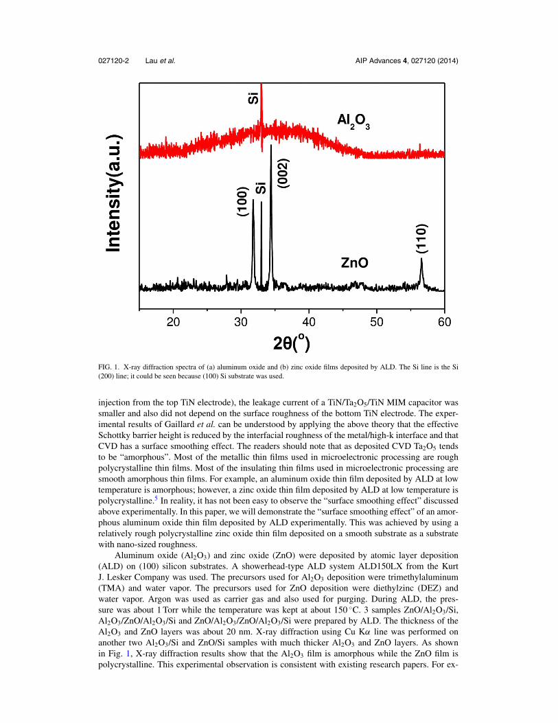
FIG. 2. Box plot of RMS surface roughness values for three samples prepared by atomic layer deposition.
ample, Gieraltowska et al. pointed out that Al2O3 film deposited by ALD tends to be amorphouswhile El-Atab et al. pointed out that ZnO film deposited by ALD tends to be polycrystalline.6, 7 Apolycrystalline film tends to be rougher than an amorphous film because of random grain growth.The purpose of using the polycrystalline ZnO film is to deliberately create some surface roughnesswhich can be suppressed by the subsequent deposition of the amorphous Al2O3 film.
Atomic force microscopy (AFM) was performed on the samples. As shown in Fig. 2, RMSsurface roughness was plotted in the form of a box plot for the 3 samples ZnO/Al2O3/Si,Al2O3/ZnO/Al2O3/Si and ZnO/Al2O3/ZnO/Al2O3/Si prepared by thermal ALD. It can be easilyseen from Fig. 2 that the sample Al2O3/ZnO/Al2O3/Si has the smallest surface roughness comparedto the samples ZnO/Al2O3/Si and ZnO/Al2O3/ZnO/Al2O3/Si. In addition, it can be easily seen fromFig. 2 that the sample Al2O3/ZnO/Al2O3/Si has the smallest statistical spread of RMS surface rough-ness compared to the samples ZnO/Al2O3/Si and ZnO/Al2O3/ZnO/Al2O3/Si. Furthermore, as shownin Fig. 2, the RMS roughness of Al2O3/ZnO/Al2O3/Si is only smaller than that of ZnO/Al2O3/Siby about 0.1 nm. This explains why it has been difficult to observe the “surface smoothing effect”experimentally before.
There exist some extra factors such that it has been difficult to observe the “surface smoothingeffect” of ALD. The readers can imagine that an experiment can be done in the following manner.A rough polycrystalline metal film is deposited by sputtering at room temperature on a smooth Sisubstrate. AFM is performed to measure the RMS surface roughness, resulting in a value of SR1.Then Al2O3 is deposited by ALD at 300 ◦C, which is significantly higher than room temperature.AFM is performed again to measure the RMS surface roughness, resulting in a value of SR2. If thereis a “surface smoothing effect”, it is expected that SR2 is smaller than SR1. However, in reality,this may not be experimentally observed; it is possible that SR2 is larger than SR1 according toexperimental observation. There are two additional factors which can affect the roughness of themetal/insulator interfacial region: (1) non-uniform oxidation of the bottom metal electrode duringthe deposition of the insulator and (2) the grain growth of the bottom metal electrode. Thesetwo important factors were discussed by Abe et al. in 2005.8 The second important factor was alsodiscussed by Alimardani et al. in 2012 when they studied the electrical characteristics of ALD Al2O3
027120-4 Lau et al. AIP Advances 4, 027120 (2014)
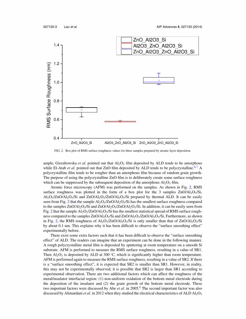
FIG. 3. XTEM micrograph of a 4-layered ZnO/Al2O3/ZnO/Al2O3/Si prepared by ALD on a Si substrate showing the surfacesmoothing effect of an amorphous thin film deposited by ALD. The Si substrate is on the right side while the Pt marker is onthe left side. The ZnO layer on the right side was used to generate some nano-sized roughness. The ZnO/Al2O3 interface onthe left side can be seen to be smoother than the Al2O3/ZnO interface on the right side.
MIM capacitors.9 Thus after ALD, the actual RMS surface roughness of the bottom metal/insulatorinterfacial region can be SR* such that SR* > SR1. SR2 may be smaller than SR* because of the“surface smoothing effect” but SR* is difficult to measure and the experimentalist may only be ableto see SR2 > SR1 instead of SR2<SR1. In this way, the confused experimentalist may not be able tosee the “surface smoothing effect” of ALD. In our work, a ZnO film was used instead of a metal filmin order to eliminate the first factor. To tackle the second factor, a relatively low ALD temperatureof 150 ◦C was chosen for both Al2O3 and ZnO such that “grain growth” of the underlying ZnO filmwas suppressed.
Cross-sectional transmission electron microscopy (XTEM) was performed on the 4-layeredZnO/Al2O3/ZnO/Al2O3/Si sample prepared by ALD. As shown in Fig. 3, the interface between thefirst Al2O3 film and Si is not sharp and smooth because of the formation of an interfacial layer. Theinterface between the second Al2O3 film and the first ZnO film is sharp but not smooth. However,the interface between the second Al2O3 film and the second ZnO film is both sharp and smooth.As shown in Fig. 3, it can be seen that the interface between the second Al2O3 film and the secondZnO film is smoother than the interface between the second Al2O3 film and the first ZnO film.In our experiment, the polycrystalline ZnO film was intended to produce some roughness and ourexperimental observation shows that the roughness produced by the polycrystalline ZnO film can besuppressed by an additional amorphous Al2O3 film deposited by ALD.
As shown in Fig. 3, the two Al2O3 layers do not appear to have the same thickness even thoughthe number of ALD cycles was the same for the two Al2O3 layers; this is also the same case for thetwo ZnO layers. Puurunen and Vandervorst pointed out that the growth per cycle (GPC) for ALDmay not be a constant; it takes some ALD cycles before the GPC becomes a constant such that theinitial GPC can be smaller than the saturated GPC.10 Thus it is possible that the two layers grown byALD do not appear to have the same thickness even though the number of ALD cycles was the samefor the two layers if the initial growth of the second layer is different from that of the first layer.
In conclusion, an amorphous thin film like Al2O3 deposited by ALD has a surface smoothingeffect on a substrate with nano-sized roughness. The readers should note that ALD is conformal
027120-5 Lau et al. AIP Advances 4, 027120 (2014)
for “large” morphological features of the underlying structure such that ALD will reproduce thesefeatures at the top interface. In this work, nano-sized roughness was produced by a polycrystallinethin film like ZnO deposited by ALD.
Lau has previously pointed out the significance of this surface smoothing effect on the I-Vcharacteristics of high-k MIM capacitors.1, 2 For example, Lukosius et al. prepared Pt/SrTiO3/Pt MIMcapacitors with the SrTiO3 thin film deposited by ALD; the I-V characteristics were asymmetrical forthese apparently symmetrical MIM capacitor structures as seen in their Fig. 4.11 The leakage currentfor electrons injected from the bottom Pt electrode appeared to be larger than that for electronsinjected from the top Pt electrode. Lukosius et al. did not give an explanation for their experimentalobservation. However, their experimental observation can be easily explained as follows. The bottomPt electrode had some surface roughness. The SrTiO3 thin film deposited by ALD according toLukosius et al. has a surface smoothing effect just like the amorphous Al2O3 thin film deposited byALD in our laboratory. (Note: SrTiO3 thin film deposited by ALD at low temperature is amorphous.)In this way, the top Pt/SrTiO3 interface is smoother than the bottom SrTiO3/Pt interface. As Laupointed out before that the effective Schottky barrier height is reduced by roughness,1 the topPt/SrTiO3 interface has a larger effective Schottky barrier height than the bottom SrTiO3/Pt interface,resulting in the asymmetrical I-V characteristics reported by Lukosius et al.11 In addition, thecombination of Al2O3 and ZnO deposited by ALD has been demonstrated to have some deviceapplications; thus the “surface smoothing” effect discussed in this paper may be relevant to thosedevices.12–14
1 W. S. Lau, ECS J. Solid State Sci. Technol. 1 N139 (2012).2 W. S. Lau, ECS Trans. 53(1) 313 (2013).3 C. Hashimoto, H. Oikawa, and N. Honma, IEEE Trans. Electron Dev. 36, 14 (1989).4 N. Gaillard, L. Pinzelli, M. Gros-Jean, and A. Bsiesy, Appl. Phys. Lett. 89, 133506 (2006).5 J. W. Elam, Z. A. Sechrist, and S. M. George, Thin Solid Films 414, 43 (2002).6 S. Gieraltowska, L. Wachnicki, B. Witkowski, M. Godlewski, and E. Guziewicz, Optica Applicata 43, 17 (2013).7 N. El-Atab, S. Alqatari, F. B. Oruc, T. Souier, M. Chiesa, A. K. Okyay, and A. Nayfeh, AIP Advances 3, 102119 (2013).8 Y. Abe, M. Kawamura, and K. Sasaki, Jpn. J. Appl. Phys. 44, 1941 (2005).9 N. Alimardani, W. W. Cowell III, J. F. Wager, J. F. Conley, Jr., D. R. Evans, M. Chin, S. J. Kilpatrick, and M. Dubey, J.
Vac. Sci. Technol. A 30, 01A113 (2012).10 R. L. Puurunen and W. Vandervorst, J. Appl. Phys. 96, 7686 (2004).11 M. Lukosius, T. Blomberg, D. Walczyk, G. Ruhl, and Ch. Wenger, IOP Conference Series: Materials Science and
Engineering 41, 012015 (2012).12 F. B. Oruc, F. Cimen, A. Rizk, M. Ghaffari, A. Nayfeh, and A. K. Okyay, IEEE Electron Dev. Lett. 33, 1714 (2012).13 N. El-Atab, A. Rizk, A. K. Okyay, and A. Nayfeh, AIP Advances 3, 112116 (2013).14 N. El-Atab, A. Ozcan, S. Alkis, A. K. Okyay, and A. Nayfeh, Appl. Phys. Lett. 104, 013112 (2014).