
Design and fabrication of a midinfrared photonic crystal defect cavity in indium antimonide
66
Proceedings of the First International Workshop on FIB for Photonics Eindhoven, the Netherlands,13-14 June 2008 Collocated with the 14th European Conference on Integrated Optics (ECIO 2008) Editors René M. de Ridder Feridun Ay Lasse J. Kauppinen
-
Upload
independent -
Category
Documents
-
view
3 -
download
0
Transcript of Design and fabrication of a midinfrared photonic crystal defect cavity in indium antimonide

Proceedings of theFirst International Workshop on
FIB for Photonics
Eindhoven, the Netherlands,13-14 June 2008
Collocated with the 14th European Conference on Integrated Optics (ECIO 2008)
Editors
René M. de RidderFeridun AyLasse J. Kauppinen

Proceedings of the
First International Workshop on
FIB for Photonics
Eindhoven, the Netherlands
13-14 June 2008
Collocated with the 14th European Conference on Integrated Optics (ECIO 2008) University of Twente Enschede, The Netherlands June 2008 ISBN: 978-90-365-2678-4

Contents Preface................................................................................................................................................ III
Workshop Programme .......................................................................................................................IV
J. Gierak, E. Bourhis, D. Mailly, R. Jede, L. Bruchhaus, S. Bauerdick, R. Colombelli, L. Aigouy, I. Robert Philip, I. Sagnes, R. Braive, S. Laurent, A. Beveratos, I. Abram, “Application of a high resolution FIB nanowriter for photonic devices patterning” (invited) ................................ 2
J. Schrauwen, J. Van Lysebettens, M. Vanhoutte, D. Van Thourhout, R. Baets, “Iodine enhanced focused ion beam etching of silicon for photonic device modification and prototyping” (invited) .......................................................................................................................... 4
G. Hobler, Heung-Bae Kim, “3D FIB Process Simulation for Photonic Applications” (invited)....... 8
W.C.L. Hopman, F. Ay, R.M. de Ridder, “Focused ion beam milling strategy for sub-micrometer holes in silicon” (invited) ............................................................................................... 12
N. Courjal, M.-P. Bernal, M. Spajer, G. Ulliac, R. Salut, J. Dahdah, S. Benchabane, “FIB milling for lithium niobate photonic crystals” (invited) .................................................................... 16
Jie Tian, Min Qiu, “Optical Quality Improvement of Si Photonic Filters Fabricated by Focused-Ion-Beam Milling”............................................................................................................................. 22
F. Causa, L. Ferraro, M. Milani, J. Sarma, F. Tatti, “FIB post-fabrication processing of Super-Luminescent Diodes”......................................................................................................................... 26
V. Callegari, P. Kaspar, P. Strasser, U. Sennhauser, H. Jäckel, “Fabrication of 2D-InP photonic crystals by means of hole-etching using focused ion beam and characterization of the hole shape, damage and surface roughness induced by the fabrication process”...................................... 30
J.R. Pugh, P.J. Heard, G.R. Nash, T. Ashley, J.G. Rarity, M.J. Cryan, “Design and Fabrication of a Mid Infra-Red Photonic Crystal Defect Laser in Indium Antimonide” ..................................... 34
I. Salakhutdinov, K. Chaganti, G.W. Auner, “Focusing diffraction gratings fabricated by FIB for integrated optics applications” ..................................................................................................... 38
R.W. Tjerkstra, F.B. Segerink, J.J. Kelly, W.L. Vos, “Focused ion beam milling of three dimensional nanostructures with high precision” .............................................................................. 42
E.J.R. Vesseur, H. Zeijlemaker, A. Polman, “Fabrication and characterization of plasmonic nanoresonators using focused-ion-beam-milling” ............................................................................. 46
F. Ay, A. Uranga, J.D.B. Bradley, K. Wörhoff, R.M. de Ridder, M. Pollnau, “Optimization of focused ion beam nanostructuring of 1-D photonic crystals in Al2O3 channel waveguide” ............ 48
I. Bayn, B. Meyler, A. Lahav, J. Salzman, B.A. Fairchild, S. Prawer, F.L. Martinez, “Diamond Photonic Crystal: Ultra-high-Q nanocavity FIB assisted fabrication” .............................................. 52
T. Thomay, T. Hanke, K. Beha, M. Hagner, A. Leitenstorfer, R. Bratschitsch, “FIB-Milling of Dielectric Pillar Microcavities with Embedded Semiconductor Quantum Dots”.............................. 56
Author index ...................................................................................................................................... 60

Preface
The first International Workshop on Focused Ion Beam (FIB) Processing for Photonics
Although FIB for applications in optics has recently become a hot topic, it has received little special attention in conference meetings. FIB has attracted interest from several research groups because of its potential for rapid prototyping of nanostructured devices, post-fabrication trimming/tuning of such devices, and its ability to mill a large variety of materials that may be hard to etch using other methods. On the other hand, several scientific and technical issues still need to be resolved, such as the optical effects of amorphisation due to the ion bombardment of a thin top layer of the processed material, the implantation of the milling ions (mostly gallium), and the best strategy for obtaining high-aspect-ratio submicrometre-sized holes (fighting redeposition effects). In addition to pure physical ion beam milling, a process that is determined by parameters such as beam current, spot size, dwell time and number of repetitions of the pattern to be milled, chemically assisted FIB processes are available for many materials. The latter processes may provide larger etch rates and diminished redeposition, although generally at the cost of reduced geometrical resolution. Determining the best process for realising a certain structure in a given materials system is not a trivial task. The workshop originates from a so-called Joint Research Activity “FIB for Photonics” in the European Network of Excellence “ePIXnet” on Photonic Integrated Components and Circuits. The papers in these proceedings by Schrauwen et al., Courjal et al., Hopman et al. and Ay et al. report on some of the results that have been obtained in this Joint Research Activity. Recognising the relevant research outside the ePIXnet community on FIB applications for optical structures, intending to bring together the scientists that are interested in this field, and aiming at disseminating recent results as well as at initiating possible new collaborations, we decided to organise this workshop and open it to the international scientific community. The organisers gratefully acknowledge the financial and/or organisational support by ePIXnet, FEI company, ECIO organising committee, Eindhoven University of Technology, and University of Twente.
Workshop Chairs and Organizers: René M. de Ridder
Feridun Ay Lasse J. Kauppinen
III

Workshop FIB for Photonics
June 13-14, 2008, Eindhoven, the Netherlands
Programme Friday 13/06/2008
15:30-16:30 Registration desk open 16:00 Refreshments
16:30-18:15 Session 1 16:30 invited: J. Gierak, “Application of a high resolution FIB nanowriter for photonic devices
patterning” 17:15 invited: J. Schrauwen, “Iodine enhanced focused ion beam etching of silicon for photonic
device modification and prototyping” 18:00 J. Tian, “Optical Quality Improvement of Si Photonic Filters Fabricated by Focused-Ion-
Beam Milling”
Saturday 14/06/2008
8:30-9:30 Registration desk open 8:30-9:00 Coffee
9:00-10:30 Session 2 9:00 invited: G. Hobler, “3D FIB Process Simulation for Photonic Applications” 9:45 F. Causa, “FIB post-fabrication processing of Super-Luminescent Diodes” 10:00 V. Callegari, “Fabrication of 2D-InP photonic crystals by means of hole-etching using
focused ion beam and characterization of the hole shape, damage and surface roughness induced by the fabrication process”
10:15 J.R. Pugh, “Design and Fabrication of a Mid Infra-Red Photonic Crystal Defect Laser in Indium Antimonide”
10:30-11:00 Coffee break
11:00-12:30 Session 3 11:00 invited: W.C.L. Hopman, “Focused ion beam milling strategy for sub-micrometer holes
in silicon” 11:45 I. Salakhutdinov, “Focusing diffraction gratings fabricated by FIB for integrated optics
applications” 12:00 R.W. Tjerkstra, “Focused ion beam milling of three dimensional nanostructures with high
precision” 12:15 E.J.R. Vesseur, “Fabrication and characterization of plasmonic nanoresonators using
focused-ion-beam-milling”
12:30-13:30 Lunch
13:30-15:00 Session 4 13:30 invited: N. Courjal/ M. Spajer, “FIB milling for lithium niobate photonic crystals” 14:15 F. Ay, “Optimization of focused ion beam nanostructuring of 1-D photonic crystals in
Al2O3 channel waveguide” 14:30 I. Bayn, “Diamond Photonic Crystal: Ultra-high-Q nanocavity FIB assisted fabrication” 14:45 T. Thomay, “FIB-Milling of Dielectric Pillar Microcavities with Embedded
Semiconductor Quantum Dots”
15:00-15:05 Closing of the workshop
IV

Application of a high resolution FIB nanowriter for photonic devices patterning J. Gierak1, E. Bourhis1, D. Mailly1 ,R.. Jede2, L. Bruchhaus2 S. Bauerdick2, R. Colombelli3, L. Aigouy4, I.
Robert Philip1, I. Sagnes1 R. Braive1, S. Laurent1, A. Beveratos1 and I. Abram1
[email protected] / CNRS, route de Nozay, F - 91460 Marcoussis
2 Raith GmbH, Hauert 18, Technologiepark, D-44227 Dortmund, Germany 3IEF - UMR 8622 - Bât. 220 - Centre Scientifique d'Orsay - F 91405 Orsay cedex
4LPEM, CNRS UPR 5, ESPCI, 10 rue Vauquelin, Paris F-75231
Introduction When FIB technology was introduced in the end of the 70's, a promising future was
immediately considered, specifically for high-resolution fabrication of photonic devices. The unique capability of FIB to allow direct resist-free and 3D controlled patterns was found to be very attractive in this rapidly growing research area. In parallel, as a result of the intensive and uninterrupted research effort, the performances of FIB instruments came quickly very close to the most advanced nanofabrication methods and therefore FIBs were intensively tested in different areas like local doping and direct machining of integrated laser devices. But some basic limitations were almost immediately observed like the spatial extension of the phenomena induced by Focused Ion Beam irradiation [1]. Following this, the realization of highly localized structures using FIB remains considered as difficult for materials very sensitive to ion-induced defects, like III-V compounds.
In this presentation we will present our work aiming at exploring the nano-structuring
potential of a highly focused pencil of ions. We will first show that a high resolution FIB nanowriter designed to specifically address sub-5 nm patterning [2] is capable to allow innovative patterning schemes for nanofabrication. We will then detail the very high resolution FIB instrument we have developed specifically to meet such nano-fabrication requirements. Finally we will detail and illustrate our efforts related to FIB processing of photonic devices:
(i) Development of combined FIB patterning techniques with epitaxial technologies aiming at minimizing the extension FIB induced defect in the vicinity of a FIB patterned semiconductor: - Epitaxial Lateral Overgrowth (ELO) technology allowing fabrication of GaN/AlGaN and GaN/GaInN heterostructures. - Localised grown InAs structures on InP and GaAs substrates using selective epitaxy (MOCVD) (ii) Engineering and tailoring of the optical properties of apertures and microcavities: - 3D near-field experimental study of the light transmitted by a hole array - FIB engineering of the optical properties of microcavities.
We will conclude this presentation by introducing some emerging concepts and principles
we have started to explore for next-generation FIB processing of photonic devices.
References [1] T. Yamamoto, J. Yanagisawa, K. Gamo, S. Takaoka, and K. Murase, Jpn. J. Appl. Phys. Vol. 32 6268 (1993) [2] J. Gierak, A. Madouri, A.L. Biance, E. Bourhis, G. Patriarche, C. Ulysse, D. Lucot, X. Lafosse, L. Auvray, L. Bruchhaus and R. Jede, Microelectronic Engineering, Volume 84, Issues 5-8, May-August 2007, 779-783.
invited Workshop FIB for Photonics, Eindhoven 2008
2

3
Iodine enhanced focused ion beam etching of silicon for photonic device modification and prototyping
Jonathan Schrauwen, Jeroen Van Lysebettens, Michiel Vanhoutte, Dries Van Thourhout and Roel Baets
Photonics research group, Department of Information Technology, Ghent University - IMEC, Sint-Pietersnieuwstraat 41, 9000 Gent, Belgium
Focused-ion-beam etching of silicon has the potential of fast and versatile fabrication of micro- and nanophotonic devices. However, large optical losses due to crystal damage and ion implantation limit the applicability of FIB in devices where the optical mode is confined near the etched region. We demonstrate a reduction of the losses by etching with iodine gas enhancement, followed by baking at 300 °C. This technique was applied for the prototyping of several grating coupler concepts and for the fabrication of slot waveguides and ring resonators.
Introduction The use of silicon as a platform for passive as well as active photonics has been an exciting research subject in recent years. The primordial advantage of silicon over III–V materials is the large amount of experience that has been built up in electronics over the past decades, the availability of large and reliable manufacturing environments, and the large refractive index contrast between silicon and oxide or air. Most of the micro- or nanophotonic structures in silicon are fabricated by a combination of optical lithography, dry and wet etching processes and layer deposition or growth. These are wafer-scale processes that enable fabrication of many devices in parallel, lowering the cost. However, due to the need for expensive masks, development of devices is costly and slow. Therefore one needs prototyping technologies that enable rapid and flexible fabrication of nanophotonic components. The best example nowadays is electron-beam lithography, which is a serial technique, too slow for the mass fabrication of large devices, but attractive as prototyping technique because of its high resolution compared to standard optical lithography. One of the inconveniences however, is the fact that electrons cannot directly etch a semiconductor. Therefore one has to work with resist layers and etch with the classical tools such as plasma etching. This slows down the optimization process and limits the designs to planar structures. An interesting alternative is focused-ion-beam (FIB), where a beam of ions is used instead of an electron beam. In current commercial systems the particle optics enables local sputtering with a spot smaller than 10 nm. There is no need for a resist, which enables post processing of devices with a more complex topography such as ridge waveguides. Furthermore, one is no longer limited to etching planar structures, e.g., by tilting the sample one can etch slanted holes or slits. As focused-ion-beam is a serial technique it is not likely to be used for mass fabrication of large area devices. However, it is a suitable technique to make small modifications to structures that were fabricated with other techniques such as optical lithography. The post processing of III–V devices by means of FIB has been reported [1-3]. In all of the examples the modal volume is big compared to the etched region. A clear deterioration of the optical properties is often observed, but can be overcome by pumping in the undamaged regions. However, in silicon one is often limited to passive devices, and wants to exploit tight confinement and small modal volumes. When a silicon device with its optical mode close to the focused-ion beam etched region is fabricated, large optical losses are observed [4-7], caused by amorphization and ion implantation of the silicon. To enhance the focused-ion-beam etch rate one can use additional gasses in the etch process [8]. In previous work we have reported that the quality of focused-ion-beam etched silicon is improved by iodine enhancement [4, 7, 9]. In this work we summarize these results and present newly fabricated devices: grating couplers and slot waveguides.
4
invited Workshop FIB for Photonics, Eindhoven 2008
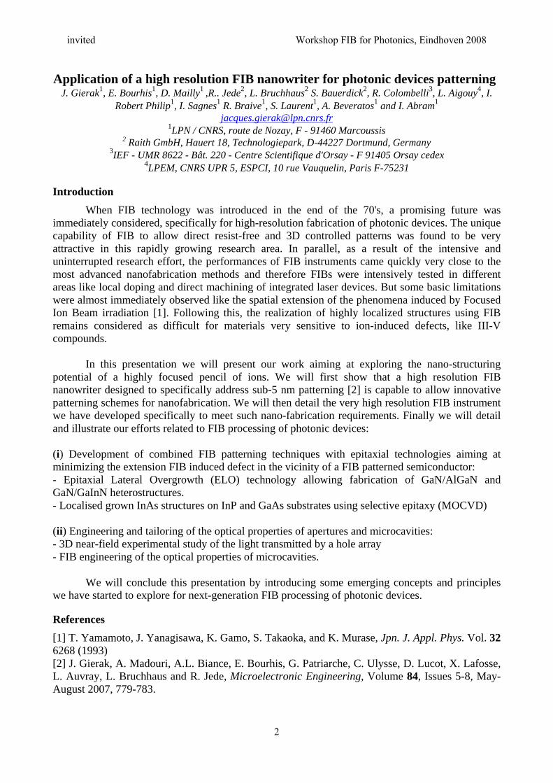
Figure 1: (a) Schematic overview of the loss measurement setup. (b) Iodine enhanced FIB etching of silicon followed by baking results in acceptable optical losses.
Iodine enhanced etching and baking Fig. 1 shows an experiment that was conducted to determine the influence of iodine etch enhancement on the losses in silicon [7]. Prefabricated waveguides were implanted and etched with FIB over varying length sections with a dose of 5 x 1015 cm-2. It was observed that iodine gas enhancement reduces the losses from 3500 to 1700 dB/cm; a further reduction to 200 dB/cm was obtained after baking for two hours in nitrogen gas at 300oC. We have confirmed by surface analysis techniques that this is caused by desorption of silicon-iodide bonds that stick to the surface. This technique was used to demonstrate several device prototypes. However, because it is difficult to achieve a trench with straight sidewalls and flat bottom using gas enhancement, we have used a 50 nm thick alumina layer as hard etch mask in all the fabricated devices.
Grating couplers Firstly we have fabricated a copy of an existing grating coupler design, previously made by deep-UV (DUV) lithography. This design consists of 315 nm wide, 70 nm deep slits with a period of 630 nm, on a 10 micron wide waveguide in the top 220 nm thick Si layer of a silicon-on-insulator wafer. The resulting grating (see Fig. 2(c)) has slightly asymmetric trenches because the enhancement gas is fed from the left. Nevertheless, the measured fiber-to-waveguide efficiency is comparable to that of the DUV fabricated original, as depicted in Fig. 2(a) [4]. Higher coupling efficiencies can be achieved by altering the grating grooves. As an example we have fabricated a slanted grating prototype, with 80 nm wide grooves at an off-normal angle of 60o (Fig. 2(b)). The experimentally measured fiber to waveguide coupling efficiency was 46 % [9]. The slits were etched using iodine gas enhancement and an alumina etch mask. A third grating concept was tested by etching thin slits on the outer radius of a ring resonator (see Fig. 3). The goal of this grating is direct fiber sensing of the power in the optical cavity, without the need for a waveguide and grating coupler. We have achieved slits with a width of less than 50 nm. Fig. 3(b) shows the transmission spectrum measured on the access waveguide of the ring with a Q factor of about 4000 for a grating with period 650 nm. However, the Q factor of this ring is not a good measure to estimate the influence of FIB losses, because it is difficult to separate the power lost by FIB etch losses from the power that is scattered and diffracted out of the optical cavity. The power measured with a fiber positioned on top of the ring grating was increased by a factor of 7 as compared to the case without grating on the ring.
5

Figure 2: (a) Fiber-to-waveguide coupling spectra for two FIB-fabricated grating couplers: (c) a copy of a DUV fabricated grating coupler and (b) a prototype of a slanted grating coupler.
Figure 3: (a) Grating etched in a ring resonator; (b) the spectrum shows Q values of around 4000 for a grating period of 650 nm.
Slot waveguides A better way to judge the optical losses in etched slits is by etching a slot along the length axis of a waveguide. This was done in DUV fabricated straight waveguides and in ring resonators (width 500nm, height 220 nm), with the purpose of making the effective index of the propagating mode more sensitive to the surrounding environment. The propagation loss in a straight slot waveguide (slot width ~ 100 nm) and coupling loss between regular and slot waveguide were measured by measuring the power transmission through slots with varying length (Fig. 4(a)), resulting in a propagation loss of about 130 dB/cm and a coupling loss of about 1.7 dB. The same slot was fabricated in a ring resonator, of which the spectrum (Fig. 4(b)) shows a cavity Q factor of about 1000. Both measurements demonstrate the relatively low losses in a FIB etched slot.
Conclusions We have developed a FIB etching technique for prototyping and post-fabrication of silicon photonic components with considerably lower losses than direct FIB etching. The technique was applied to fabricate various grating couplers and slot waveguides and ring resonators.
6

Figure 4: (a) Measurement of the propagation losses in a FIB etched slot in a pre-fabricated waveguide, (b) spectrum of a slot ring resonator and (c) a cross-sectional micrograph of the etched slot.
Acknowledgements This work was partly supported by the European Network of Excellence ePIXnet and by the Fund for Scientific research (FWO).
References [1] S. Rennon, L. Bach, H. Konig, J. P. Reithmaier, A. Forchel, J. L. Gentner and L. Goldstein, Nanoscale patterning by focused ion beam enhanced etching for optoelectronic device fabrication Microelectron. Eng. 57–58, 891 (2001). [2] A. J. Steckl and I. Chyr, Focused ion beam micromilling of GaN and related substrate materials (sapphire, SiC, and Si), J. Vac. Sci. Technol. B 17, 362 (1999). [3] Q. Ren, B. Zhang, J. Xu, Z. S. Zhang, Y. B. Jin, Y. Qian, and D. P. Yu, Etched facet and semiconductor/air DBR facet of a AlGaInP laser diode prepared by focused ion beam milling, Solid State Commun. 130, 433 (2004). [4] J. Schrauwen, D. Van Thourhout, and R. Baets, Focused-ion-beam fabricated vertical fiber couplers on silicon-on-insulator waveguides, Appl. Phys. Lett. 89, 141102 (2006). [5] D. J. Moss, V. G. Ta’eed, B. J. Eggleton, D. Freeman, S. Madden, M. Samoc, B. Luther-Davies, S. Janz, and D. X. Xu, Bragg gratings in silicon-on-insulator waveguides by focused ion beam milling, Appl. Phys. Lett. 85, 4860 (2004). [6] Y. Tanaka, M. Tymczenko, T. Asano, and S. Noda, Fabrication of two-dimensional photonic crystal slab point-defect cavity employing local three-dimensional structures, Jpn. J. Appl. Phys., Part 1 45, 6096 (2006). [7] J. Schrauwen, D. Van Thourhout and R. Baets, Iodine enhanced focused-ion-beam etching of silicon for photonic applications, J. Appl. Phys. 102, 103104 (2007). [8] K. Edinger and T. Kraus, Modeling of focused ion beam induced chemistry and comparison with experimental data, Microelectron. Eng. 57–58, 263 (2001). [9] J. Schrauwen, F. Van Laere, D. Van Thourhout and R. Baets, Focused-ion-beam fabrication of slanted grating couplers in silicon-on-insulator waveguides, Phot. Technol. Lett., 19, 816-818 (2007)
7

3D FIB Process Simulation for Photonic Applications Gerhard Hobler1 and Heung-Bae Kim2
1 Vienna University of Technology, Institute of Solid State Electronics, Floragasse 7, A-1040 Vienna, Austria [email protected]
2 FEI Company, 5350 NE Dawson Creek Dr., Hillsboro, OR 97124, USA
A simulation-based approach to the fabrication of photonic structures by FIB can be useful to determine the optimum process parameters like scan strategy, dwell times, and beam properties. In this contribution we present the recently developed simulation software AMADEUS. We give two examples of the application of AMADEUS 3D to the fabrication of photonic structures. Finally, we discuss the need for additional simulation capabilities, which are either under development or planned as future work.
Introduction Accurate fabrication of photonic components such as lenses, gratings, and photonic crystals is necessary for emerging applications. Focused ion beams (FIB) offer a relatively simple solution without photoresist and additional etching processes. The precise realization of the desired structures, however, is not straightforward, since the surface evolution during FIB processing depends on various parameters like scan strategy, dwell times, and beam current distribution. The main physical mechanisms responsible are the angular dependence of the sputtering yield and the redeposition of already sputtered material. We have previously developed a 2D and 3D simulation software, AMADEUS 2D/3D [1,2], which takes both effects into account. In this contribution we present two applications to photonic structures using a new feature of AMADEUS 3D that allows arbitrary scan strategies. In addition, we discuss future directions for the development of simulation capabilities.
AMADEUS 3D In AMADEUS 3D the surface is represented by nodes which move with a velocity determined by the incident ion flux and the redeposition fluxes. The efficiency of the incident ion flux for eroding the surface is described by the sputtering yield Y(θ) which is a function of the incidence angle θ. The redeposition flux at node i is obtained by integrating the redeposition fluxes originating from the vicinity of all other visible nodes j. These fluxes depend on the flux of sputtered atoms at node j, on the angular distribution f(α) of the sputtered atoms at node j, on the distance between the nodes, and on the angles α and β between the line of sight and the surface normals at node j and i, respectively. The angular distribution f(α) of sputtered atoms is approximated by the cosine rule f(α)~cosα. The resulting motion of the nodes is traced over time using finite time steps. Further details are described in Ref. [2]. In order to allow arbitrary scan strategies, an option has been implemented to read the pixel positions and dwell times from a file. The file can easily be generated by an external program. Among the grid strategies presented in Ref. [2] we prefer the regular grid for non-overhanging structures with restructuring after each time step. The nodes are initially arranged in a regular orthogonal grid in the x-y plane. Due to sputtering and redeposition the nodes move perpendicular to the local surface, but the resulting surface is then interpolated back to the original x-y grid. In the examples presented in the next section, we used an equidistant grid throughout the simulation which avoids the time necessary for inserting additional lines. Furthermore, the visibility check between nodes was simplified to only checking whether the line of sight emerges and ends on the vacuum side of the surface. This procedure is sufficient in many cases. With these choices typical simulation times were about 10 minutes on a PC (640 time steps, 3721 nodes).
8
invited Workshop FIB for Photonics, Eindhoven 2008
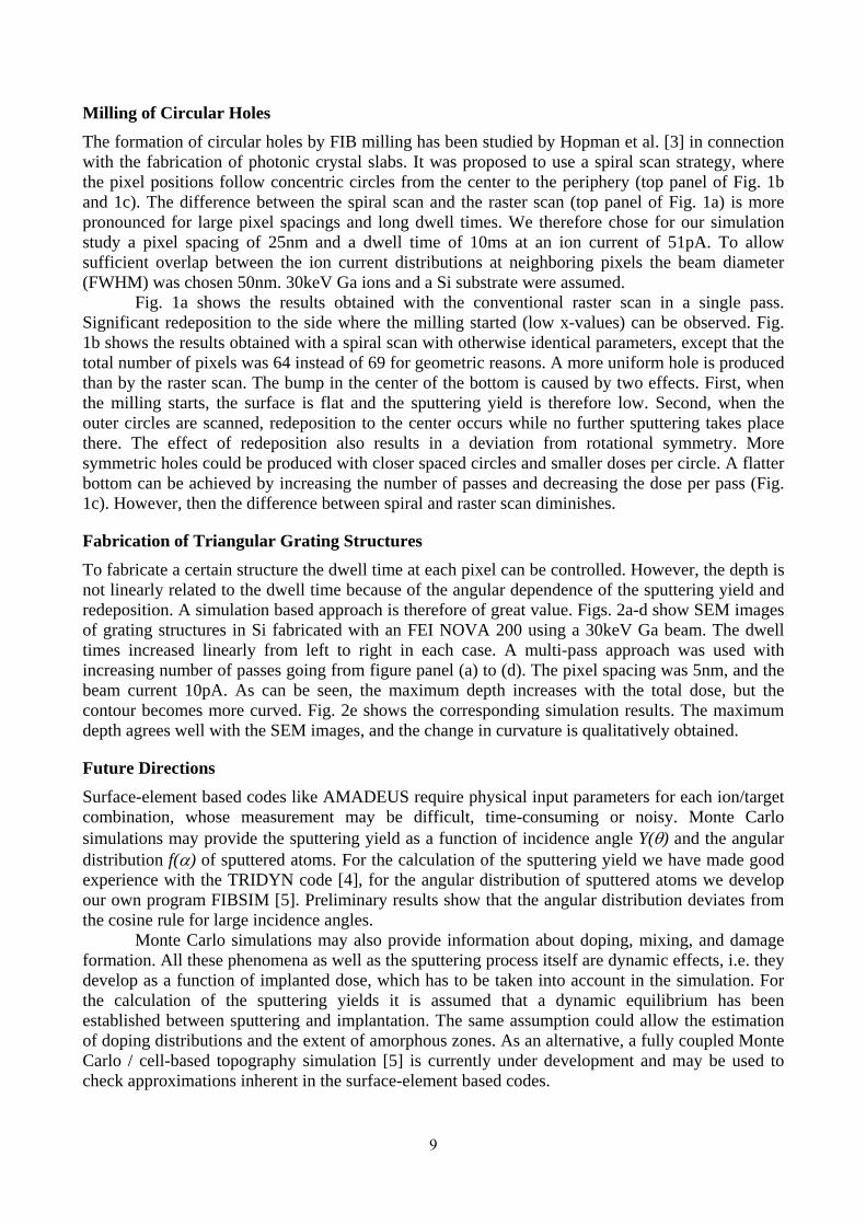
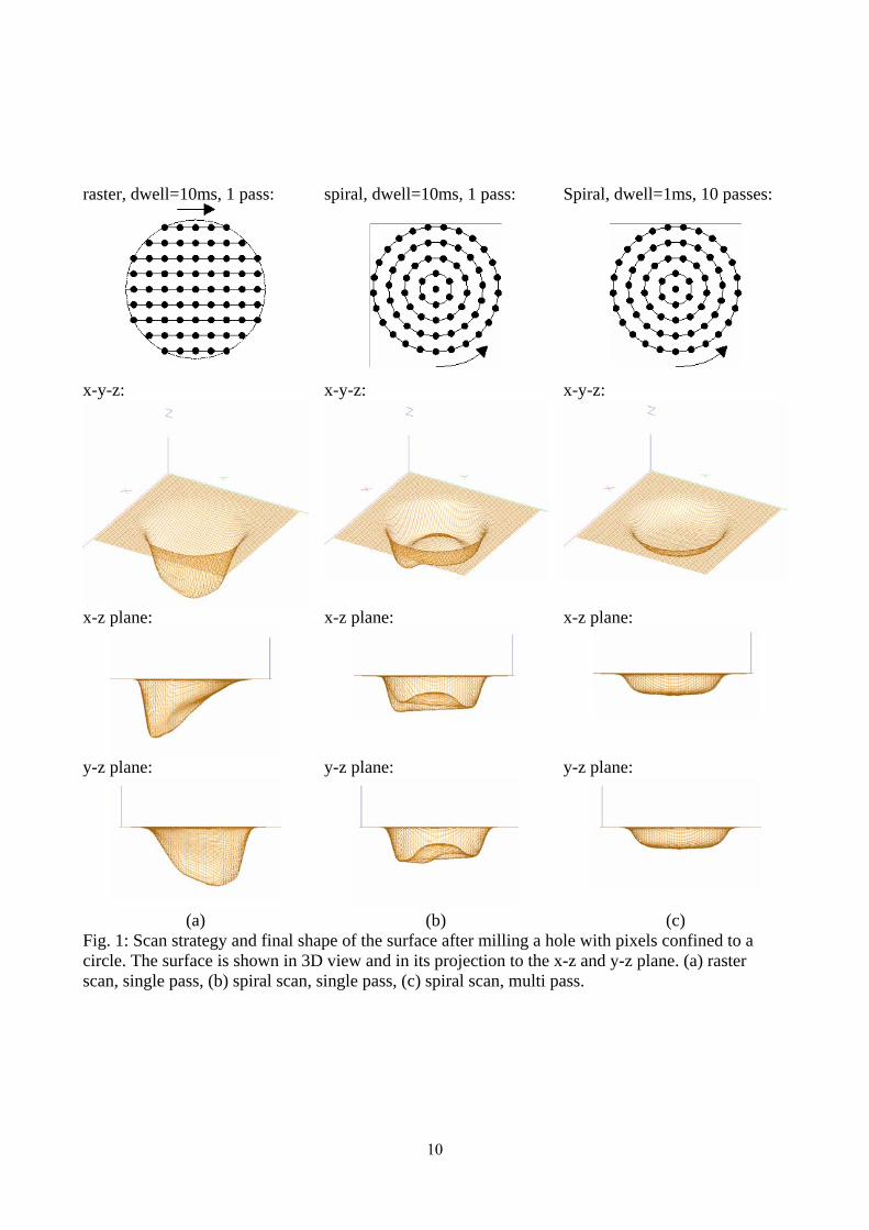
Milling of Circular Holes The formation of circular holes by FIB milling has been studied by Hopman et al. [3] in connection with the fabrication of photonic crystal slabs. It was proposed to use a spiral scan strategy, where the pixel positions follow concentric circles from the center to the periphery (top panel of Fig. 1b and 1c). The difference between the spiral scan and the raster scan (top panel of Fig. 1a) is more pronounced for large pixel spacings and long dwell times. We therefore chose for our simulation study a pixel spacing of 25nm and a dwell time of 10ms at an ion current of 51pA. To allow sufficient overlap between the ion current distributions at neighboring pixels the beam diameter (FWHM) was chosen 50nm. 30keV Ga ions and a Si substrate were assumed. Fig. 1a shows the results obtained with the conventional raster scan in a single pass. Significant redeposition to the side where the milling started (low x-values) can be observed. Fig. 1b shows the results obtained with a spiral scan with otherwise identical parameters, except that the total number of pixels was 64 instead of 69 for geometric reasons. A more uniform hole is produced than by the raster scan. The bump in the center of the bottom is caused by two effects. First, when the milling starts, the surface is flat and the sputtering yield is therefore low. Second, when the outer circles are scanned, redeposition to the center occurs while no further sputtering takes place there. The effect of redeposition also results in a deviation from rotational symmetry. More symmetric holes could be produced with closer spaced circles and smaller doses per circle. A flatter bottom can be achieved by increasing the number of passes and decreasing the dose per pass (Fig. 1c). However, then the difference between spiral and raster scan diminishes.
Fabrication of Triangular Grating Structures To fabricate a certain structure the dwell time at each pixel can be controlled. However, the depth is not linearly related to the dwell time because of the angular dependence of the sputtering yield and redeposition. A simulation based approach is therefore of great value. Figs. 2a-d show SEM images of grating structures in Si fabricated with an FEI NOVA 200 using a 30keV Ga beam. The dwell times increased linearly from left to right in each case. A multi-pass approach was used with increasing number of passes going from figure panel (a) to (d). The pixel spacing was 5nm, and the beam current 10pA. As can be seen, the maximum depth increases with the total dose, but the contour becomes more curved. Fig. 2e shows the corresponding simulation results. The maximum depth agrees well with the SEM images, and the change in curvature is qualitatively obtained.
Future Directions Surface-element based codes like AMADEUS require physical input parameters for each ion/target combination, whose measurement may be difficult, time-consuming or noisy. Monte Carlo simulations may provide the sputtering yield as a function of incidence angle Y(θ) and the angular distribution f(α) of sputtered atoms. For the calculation of the sputtering yield we have made good experience with the TRIDYN code [4], for the angular distribution of sputtered atoms we develop our own program FIBSIM [5]. Preliminary results show that the angular distribution deviates from the cosine rule for large incidence angles. Monte Carlo simulations may also provide information about doping, mixing, and damage formation. All these phenomena as well as the sputtering process itself are dynamic effects, i.e. they develop as a function of implanted dose, which has to be taken into account in the simulation. For the calculation of the sputtering yields it is assumed that a dynamic equilibrium has been established between sputtering and implantation. The same assumption could allow the estimation of doping distributions and the extent of amorphous zones. As an alternative, a fully coupled Monte Carlo / cell-based topography simulation [5] is currently under development and may be used to check approximations inherent in the surface-element based codes.
9
raster, dwell=10ms, 1 pass:
spiral, dwell=10ms, 1 pass:
Spiral, dwell=1ms, 10 passes:
x-y-z:
x-y-z: x-y-z:
x-z plane:
x-z plane:
x-z plane:
y-z plane:
y-z plane:
y-z plane:
(a) (b) (c) Fig. 1: Scan strategy and final shape of the surface after milling a hole with pixels confined to a circle. The surface is shown in 3D view and in its projection to the x-z and y-z plane. (a) raster scan, single pass, (b) spiral scan, single pass, (c) spiral scan, multi pass.
10

(e)
Fig. 2: Grating structures fabricated with the concept of variable dwell time. The dwell times increase linearly from left to right. (a)-(d) SEM images with increasing total dose. The value below each image indicates the maximum depth. (e) Simulation results corresponding to (a)-(d). Another important direction of software development is the automatic determination of process parameters for a desired geometry. We have previously optimized the shape of a blazed grating structure fabricated by a single-pass FIB mill [6]. In this work we performed a two-dimensional matrix of simulations for a range of dwell times and pixel spacings. From the resulting “response surface” of the nonplanarity of the sidewall, we were able to select parameter values for the desired planar surface. More refined methods are needed, e.g., to determine the optimum dwell times for a variable dwell-time approach. Finally, we mention the lack of models for chemically assisted FIB processing. Ion-beam induced etching and deposition are attractive options to expand the capabilities of FIB milling. Efforts in this field are currently under way by IMS Nanofabrication, Vienna, [7] in collaboration with the first author. The activities at IMS Nanofabrication are focused on ion multi-beam processing [8].
References [1] H.-B. Kim, G. Hobler, A. Lugstein, and E. Bertagnolli, J. Micromech. Microeng. 17, 1178-1183 (2007).
[2] H.-B. Kim, G. Hobler, A. Steiger, A. Lugstein, and E. Bertagnolli, Nanotechnology 18, 245303 (2007).
[3] W. C. Hopman et al., Nanotechnology 18, 195305 (2007).
[4] W. Möller and M. Posselt, TRIDYN_FZR User Manual, Forschungszentrum Rossendorf (2002).
[5] W. Boxleitner and G. Hobler, Nucl. Instr. Meth. B 180, 125-129 (2001).
[6] H.-B- Kim, G. Hobler, A. Steiger, A. Lugstein, and E. Bertagnolli, Opt. Expr. 15, 9444-9449 (2007).
[7] C. Ebm et al., to be published.
[8] E. Platzgummer, H. Loeschner, and G. Gross, Proc. SPIE Photomask/BACUS (2007) and BACUS Newsletter (March 2008).
11
Focused ion beam milling strategy for sub-micrometer holes in silicon Wico C.L. Hopman1, Feridun Ay2, René M. de Ridder2
1 Sensata Technologies, Kolthofsingel 8, 7602 EM Almelo, The Netherlands
[email protected] 2 University of Twente, Integrated Optical Microsystems, 7500 AE Enschede, The Netherlands
Focused ion beam (FIB) milling can be used as a tool to fabricate structures with sub-micrometer details. The slab material can be silicon, for example, which can then be used as a mould for nano-imprint lithography, or in silicon on insulator (SOI) layer configuration suitable for photonic applications. In the latter, additional effort has to be taken to prevent high FIB induced losses, due to ion implantation and material crystal damage. Perfectly vertical sidewalls are, in principle, required for photonic crystal applications to guarantee low-loss propagation; sidewall angles of 5 degrees can already induce a 8 dB/mm propagation loss. We report on optimization of the sidewall angle (FIB) fabricated sub-micron diameter holes. Our best case results show that sidewall angles as small as 1.5 degree are possible in Si membranes and 5 degree for (bulk) Si and SOI by applying larger doses and using a spiral scan method.
Introduction
Focused ion beam (FIB) milling is since long a mature and commonly used fabrication method [1] for micro and nanofabrication. Most recent advances are highlighted in the following review papers [2-5]. Originally, FIB processing was used for mask repair, modification of electronic integrated circuits, and sample preparation for transmission electron microscopy. Besides these applications, FIB milling can also be used to structure hard-to-etch materials like SiC or LiNbO3. FIB processing can be used to locally sputter etch, ion implant, and deposit metals and insulators with a feature size in the order of nanometers, without the need of a mask [5]. In the field of optoelectronics FIB processing has been applied, for example, for fabrication of micro-optical components with low surface roughness [6], defining the end facet mirrors for conventional semiconductor lasers [7], bulk micromachining of macro-porous silicon in order to fabricate 3D Yablonovite-like photonic crystals [9], and for fabricating 2D periodic metal nanostructures [9]. Direct milling of photonic structures in silicon on insulator (SOI) is still in an early state of maturity, due to the high ion-induced losses by amorphization of the originally crystalline Si [10] and implantation of gallium ions within the sample [11]. However, some recent results have been achieved in lowering the losses by either using etch-assisting gasses [12] or heat-treatments for out-diffusion of ions [13], which may lead to breakthroughs on this subject. The damaged and implanted Si at the Si–air interface may be removed by wet chemical etching [14]. On the other hand, FIB processing is an ideal candidate for fabrication of moulds which can, in combination of nano-imprint technology be exploited for low loss photonic devices. The smoothening effect of FIB processing [15] can then be used for creating nanosmooth moulds and replicas. Perfectly vertical sidewalls are, in principle, required for photonic crystal applications to guarantee low-loss propagation; sidewall angles of 5 degrees in photonic crystal waveguides, can already induce a 8 dB/mm propagation loss [16]. However, FIB milling of submicron holes in silicon with perfectly vertical sidewalls is challenging due to proximity effects (ion scattering) and redeposition effects: sputtered Si atoms or clusters can be redeposited locally. This effect is less pronounced in the milling of slits (or trenches), where sidewall angles down to a few degrees have been realized at low currents. In the research presented here, we studied the milling of both isolated holes and hole arrays. The sidewall angles were optimized by experimentally investigating the influence of the beam scanning routine and applied ion dose. Our best case results show that sidewall angles as small as 1.5 degree are possible in Si membranes using a spiral scan method. For Si and SOI, sidewall angles as small
12
invited Workshop FIB for Photonics, Eindhoven 2008
as 5 degrees in (bulk) Si and SOI can be found [17] by applying larger doses. All experiments were performed on a FEI Nova 600 dual beam FIB machine with a liquid metal Ga+ ion source, using an acceleration voltage of 30 kV.
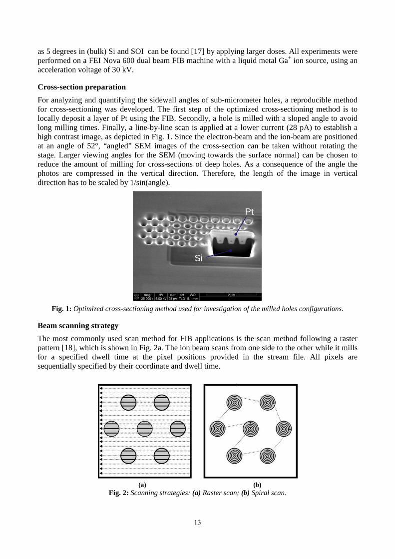
Cross-section preparation
For analyzing and quantifying the sidewall angles of sub-micrometer holes, a reproducible method for cross-sectioning was developed. The first step of the optimized cross-sectioning method is to locally deposit a layer of Pt using the FIB. Secondly, a hole is milled with a sloped angle to avoid long milling times. Finally, a line-by-line scan is applied at a lower current (28 pA) to establish a high contrast image, as depicted in Fig. 1. Since the electron-beam and the ion-beam are positioned at an angle of 52°, “angled” SEM images of the cross-section can be taken without rotating the stage. Larger viewing angles for the SEM (moving towards the surface normal) can be chosen to reduce the amount of milling for cross-sections of deep holes. As a consequence of the angle the photos are compressed in the vertical direction. Therefore, the length of the image in vertical direction has to be scaled by 1/sin(angle).
Pt
Si
Fig. 1: Optimized cross-sectioning method used for investigation of the milled holes configurations.
Beam scanning strategy
The most commonly used scan method for FIB applications is the scan method following a raster pattern [18], which is shown in Fig. 2a. The ion beam scans from one side to the other while it mills for a specified dwell time at the pixel positions provided in the stream file. All pixels are sequentially specified by their coordinate and dwell time.
(a) (b)
Fig. 2: Scanning strategies: (a) Raster scan; (b) Spiral scan.
13

Since the beam is not switched off between the holes causing nominally unmilled regions to be exposed directly by the beam when it passes over the region between two holes. During this transition a small dose of gallium is implanted, which can have a strong effect on optical absorption. If the beam crosses over repeatedly, at some point also interhole milling occurs. A better scan-routine alternative is spiral scanning for milling a single or multihole geometry. A schematic drawing of the spiral scan is shown in Fig. 2b. Another drawback of the ion beam following the raster pattern is that the beam always moves in a predefined direction while milling (from right to left as illustrated by Fig. 2a). This leads to asymmetrically shaped holes, as demonstrated in Fig. 3a, while the shape produced by the spiral scan (Fig. 3b) is much more symmetric. The third benefit of the spiral scanning pattern is the improvement found in the sidewall angle steepness. Because the beam moves from the centre of the hole outwards, redeposition at the hole boundary is milled away in the process. The average deviation from verticality of the left and right sidewall, measured halfway the depth of the hole was 19° for raster scan and 13° for the spiral scan in bulk silicon, with the milling parameters specified in the caption of Fig. 3.
(a) (b)
Fig. 3: SEM images, comparing 250 nm diameter holes in a triangular lattice with 440 nm pitch, milled into bulk silicon using different scanning strategies. (a) Raster scan; (b) Spiral scan. The insets show cross-sections.Both patterns have been milled using approximately the same dose of 70 pC per hole, with 48 pA ion beam current (e–1 spot diameter ~18 nm), 0.1 ms dwell time per pixel, and repeating the pattern in 12 loops. Both the overview images and the cross-sections were taken at 52° from the surface normal.
Fig. 4: Holes milled into a 220 nm thick silicon membrane using a spiral scan, 48 pA ion beam current, 0.1
ms dwell time, and 20 loops. The membrane was suspended over a bulk silicon substrate, in which holes can be seen below the membrane, that are due to intentional over-milling the holes in the membrane. The SEM image was taken at 30° from the surface normal. The deviation from verticality of the sidewalls is <1.5°.
14
Figure 4 shows milling results for a 220 nm thick silicon membrane. The milled material can escape both towards the bottom and to the top of the holes, reducing redeposition. In combination with applying an “over-dose” of about 115 pC per hole, a sidewall angle deviation smaller than 1.5° can be obtained.
Conclusions
We have investigated two ion beam scanning routines: scanning in a raster and spiral pattern. For benchmarking spiral against raster scanning, we used an optimized cross-sectioning technique and analyzed the average side wall angles of the holes. The results show that the quality of submicron holes milled using focused ion beam milling, can be improved by choosing spiral scanning. In particular, the symmetry and the steepness of the sidewalls were improved due to better control over the redeposition. Almost perfect vertical sidewalls can be obtained by FIB-milling of holes in Si membranes, since the otherwise redeposited milled material can more easily escape from the hole. With some over-milling, the deviation from verticality of the sidewalls of holes in a silicon membrane could be reduced to less than 1.5°.
Acknowledgments
This research was supported by NanoNed, a national nanotechnology program coordinated by the Dutch ministry of Economic Affairs, and was also supported by the European Network of Excellence ePIXnet. We thank Vishwas Gadgil for his help with operating the FIB machine and Wenbin Hu for her contribution to the development of scanning routines. The stimulating discussions with Kobus Kuipers and Markus Pollnau are also gratefully acknowledged.
References
[1] R.L. Seliger, et al., Appl. Phys. Lett. 34, 310-312 (1979). [2] A.A. Tseng, Small 1, 924-939 (2005). [3] A.A. Tseng, J. Micromech. Microeng. 14, R15-R34 (2004). [4] F. Watt, et al., Int. J. Nanosci. 4, 269-286 (2005). [5] S. Reyntjens and R. Puers, J. Micromech. Micro-eng. 11, 287-300 (2001). [6] Y. Fu and N.K.A. Bryan, J. Vac. Sci. Technol. B 19, 1259-63 (2001). [7] T. Ito, H. Ishikawa, T. Egawa, et al, Jpn. J. Appl. Phys. 36, 7710-11 (1997). [8] A. Chelnokov, K. Wang, S. Rowson, et al., Appl. Phys. Lett. 77, 2943-45 (2000). [9] K.J.K. Klein Koerkamp, S. Enoch, F.B. Segerink, et al., Phys. Rev. Lett. 92, 183901 (2004) [10] Pellerin J G, Shedd G M, D.P. Griffis, et al., J. Vac. Sci. Technol. B 7, 1810-12 (1989). [11] A.P. Knights and G.E. Hopper, Electron. Lett. 39, 1648-49 (2003). [12] J. Schrauwen, D. van Thourhout and R. Baets, Appl. Phys. Lett. 89, 141102 (2006). [13] T. Tanaka, M. Tymczenko, T. Asano and S. Noda, Jpn. J. Appl. Phys. Part 1 45, 6096-02 (2006) [14] C. Lehrer, L. Frey, S. Petersen, et al., J. Vac. Sci. Technol. B 22, 1402-06 (2004). [15] W.C.L. Hopman, R.M. de Ridder, S. Selvaraja, et al., Photonics Europe (Strasbourg), Proc. SPIE 6182, 167-73 (2006). [16] Y. Tanaka, T. Asano, Y. Akahane, et al., Appl. Phys. Lett. 82, 1661-63 (2003). [17] W.C.L. Hopman, F.Ay, W. Hu, et al., Nanotechnol. 18, 195305-11 (2007). [18] Y. Q. Fu, et al, Int. J. Adv. Manuf. Technol 16, 877-880 (2000).
15
FIB milling for lithium niobate photonic crystals Nadège Courjal, Maria-Pilar Bernal, Michel Spajer, Gwenn Ulliac, Roland Salut,
Jean Dahdah, and Sarah Benchabane Université de Franche-Comté, Institut FEMTO-ST (UMR61-74), Département
d’Optique P.M. Duffieux, 25030 Besançon Cedex, France [email protected]
Nanometric optical LiNbO3 structures are difficult to achieve, due to the resistance of the material to standard etching processes. We report on two methods based on Focused Ion Beam (FIB) milling that enable the fabrication of nanostructures in lithium niobate substrates with aspect ratio (depth-over-diameter) larger than 3:1. The first method is based on direct FIB writing and can yield the fabrication of holes with depth of 3µm and diameter of 1µm or less. The second method consists in FIB patterning of a mask which is deposited on the substrate. This process is followed by proton exchange (PE) and reactive ionic etching (RIE). Thus, structures with a diameter of 400 nm and an aspect ratio of 3:1 have been fabricated. These methods open the way to miniature electro-optical and acousto-optical modulators. Introduction Lithium niobate waveguides are used extensively in integrated optics, owing to their low optical losses, and their large electro-optical, nonlinear and acousto-optical coefficients [1]. However, the typical size of the devices (1cm or more) usually represents a significant impediment for their integration into optical circuits. Recently, photonic LiNbO3 nanostructures were demonstrated to be a solution for ensuring the fabrication of miniature LiNbO3 components [2]. Another appealing perspective that arises with the capability of nanostructuring LiNbO3 substrates is the development of new types of components, like microring resonators [3], integrated squeezing circuits [4] or devices based on photo-phononic interactions [5]. Additionally, theoretical studies have shown the considerable potential for further developments of LiNbO3 photonic crystals (PCs) [6,7]. Therefore, numerous researches have been dedicated to the achievement of nanometric optical structures, despite the well-known resistance of the material to standard etching processes. Domain engineering followed by wet etching has lead to the demonstration of submicrometric holes, but the method is limited to Z-cut substrates [8]. An alternative approach relies on ultrafast laser machining, which is amenable to patterning any material with trenches as deep as several hundreds of micrometers. A recent paper has shown the feasibility of the technique for the fabrication of polaritonic structures in LiNbO3 substrates [9]. But the application of the method to photonic structure is still challenging, because it requires the laser spot to be focused near the diffraction limits. Another common approach consists in preparing the etching of the substrate by modifying the crystal lattice [10-15]. This preparation is followed by wet or dry etching. Though widely used for the fabrication of micrometric structures like ridges, these methods are difficult to apply at nanometric scales. Nevertheless, with an appropriate choice of etching parameters, the method based on proton exchange followed by Reactive Ionic Etching (RIE) or Inductively Coupled-Plasma-RIE (ICP-RIE) has shown to be applicable to the fabrication of photonic crystals (PCs) [13,14]. Such a method implies a consequent number of steps, including the patterning of the mask by electron beam lithography followed by RIE, the proton exchange step and
16
invited Workshop FIB for Photonics, Eindhoven 2008

finally the dry etching step. Here we propose to write the patterns directly in the mask by FIB, which avoids the e-beam lithography and the RIE of the mask. An alternative consist in a direct FIB patterning of the substrate. In this paper, we report the exploitation of both methods for the fabrication photonic crystal structures. Fabr ication of lithium niobate photonic crystals The two fabrication processes are based on FIB milling. In both cases, the substrate may be either an X-cut or a Z-cut wafer. The tests were performed on samples with an area of 1cm2 and a thickness of 500µm. The FIB system is an Orsay Physics LEO FIB4400 machine, with Ga+ liquid metal ion source (LMIS). The ion acceleration energy is 30keV. The ions are focused with electrostatic lenses on the sample with a probe current 50-60pA. The pseudo-Gaussian shaped spot size is estimated to be 40nm on the target. The FIB is scanned on the sample by a computer-controlled deflection field to produce the desired pattern (Elphy Quantum from Raith). (a) (b) (c)
Figure 1 : SEM view of FIB cross-sections performed in LiNbO3 photonic crystals, tilt = 52° (a) Triangular arrangement of 23x30 holes with a diameter of 275nm
(b) Triangular arrangement of 4x4holes with diameter of 540nm, and depth of 1µm (c) Bragg gratings with a period of 1µm and a depth of 3µm
The first method relies on direct FIB patterning of the substrate. This method was firstly employed by S. Yin et al. to etch-submicrometric 1D LiNbO3 structures in 1999 [16]. In ref. [17], we have extended the method to the fabrication of 2D PCs with depth of 2µm. The method begins with the sputtering of a Cr layer with a thickness of 15nm on to the substrate. The layer is grounded with a conductive past before introduction into the FIB vacuum chamber (pressure = 2 x 10⁻⁶ Torr). The holes are milled by multiple exposures. Typically, the achievement of a hole with a width of 400nm and a depth of 2µm requires fifty loops. Indeed, multiple exposures are mandatory to avoid redeposition of the material in the neighborhood. The dwell time is 0.5ms, the step size is 11,4nm and the total exposure time is typically 2 hours for a 15x15 array of holes. With this method, we have managed to obtain matrices with holes as small as 180nm, and depth larger than 1µm. A few cross-sections of different realizations are shown in figure 1. Figure 1a) shows a triangular array of 23x30 holes with a depth of 1µm and a diameter of 270nm for the development of Er-doped microcomponents. In figure 2b) and 2c), we can see that depths of 2 or 3µm can be
3µm
500nm
2µm
275nm
17

reached when the period is of the order of 1µm. As it can be observed in figure 1 (a) and (b), the arrays exhibit well defined circular holes. The conical shape seen in the images is intrinsic to the method, and cannot be improved, unless by using additional gases that would help removing Nb from the etched substrate. In ref. [18,19], our team has demonstrated that photonic bandgap structures could be obtained with this method, despite the conical shape of the holes. A second method based on PE and RIE was then developed to reduce the fabrication time linked to the FIB process, and to fight against the conical shape of the holes. Indeed, the fabrication of 100x50 holes would require 44h of total FIB exposure, which is unacceptable. The first step of the second method consists in sputtering a 650nm thick layer of poly-silicon onto the substrate. The sample is then introduced into the FIB vacuum chamber. The parameters for etching are the same as previously described, expecting the dwell time which is reduced to 0.2ms, and the number of exposure, which is now of 30. The method is followed by proton exchange (PE) in molten benzoic acid at 190°C. Typically, an exchanged depth of 1,5µm corresponds to a 6,5h duration of proton exchange for X-cut substrates. This step is essential to produce a significant lattice deformation which facilitates the further etching. Moreover, the replacement of Li+ ions with H+ ions helps preventing from LiF redeposition during the etching step, which plays a role in both the verticality of the substrate and the etch-rate. The pattern is then written into the substrate by CHF3 RIE etching with a Plassys reactor. In order to enhance the chemical aspect of the RIE etching, we work with CHF3 at pressures of 25-100µbar, and RF power levels of 50-150W. The role of each parameter is detailed in ref. [14]. After two hours of RIE at 100W RF power and 60µbar operated pressure, we have achieved matrices with holes of 420nm diameter and of 1,2µm depth. The side wall verticality is of the same order as that achieved by direct FIB patterning, but it should be improved by replacing the RIE step with an ICP-RIE step, which is currently under test. With such parameters, the total exposure time for a matrix of 100x50 holes is reduced to 10h for the FIB exposure, in addition to the 6,5hours of proton exchange and 2 hours of RIE etching. Thus, the total duration of the process is 19h that can be advantageously compared with the 44 hours associated with direct FIB milling. This method is currently under test for the fabrication of photonic bandgap structures.
(a) (b) Figure 2: SEM images of patterns, tilt = 50°. (a) Cross-view of the polysilicon mask after FIB
milling. (b) Image of an X-cut substrate after etching of the Si mask layer, and 120 min of RIE etching. Pressure = 60 µbar – Power = 100 W Resulting depth = 1.2 µm.
1,2µm
420nm
85°
18

Exper imental character ization The first method was applied to the fabrication of electro-optic and acousto-optic modulators. An overview of the electro-optic structures is given in figure 3(a). It relies on a photonic crystal surrounded by capacitive electrodes. The photonic crystal structure is determined so that it exhibits an optical gap in the transmission response with an edge at 1550nm. The photonic crystal is made of a square array of holes, which enables slow light effects [18]. A DC power supply is connected to the electrodes via a printed circuit board and wire bonding. An applied voltage induces a change in the refractive index, which controls the spectral position of the optical gap. Thus, an intensity modulation can be achieved at 1550nm, with a driving voltage of 13,5V and an extinction ratio of 5,2dB (see fig. 3b). Following the same scheme, we have also developed acousto-optic modulators operating at 191,2MHz. The structures will be presented during the talk.
(a) (b)
Figure 3: Electro-optic photonic crystal modulators. (a) SEM view of the photonic crystal and picture of the connected PC modulator. (b) Experimental figure of modulation
Conclusion
We have developed two methods for nanostructuring LiNbO3 substrates. The two methods are well-suited for the fabrication of holes with diameter as small as 180nm, for either X-cut or Z-cut substrates. Aspect ratio of 3:1 or more have been achieved with both methods. The first method, based on direct FIB patterning, is adequate for field of photonic crystals smaller than 100x100 µm2. The second method implies using the FIB as a lithographic tool that patterns a poly-silicon mask. In this case, subsequent steps of proton exchange and CHF3 RIE are required. This method shows out to be interesting for structures exhibiting more than 500 holes. The methods enable the fabrication of new miniature modulators, with active length of only 13µm.
References
[1] L. Lawrence, Rep. Prog. Phys. 56, p. 363 (1993) [2] M. Roussey, M-P. Bernal, N. Courjal, F.I. Baida, R. Salut, Appl. Phys. Lett. 89 , 241110 (2006) [3] A. Guarino, G. Poberaj, D. Rezzonico, R. Degl’ Innocenti and P. Günter, Nature Photonics, 1, 407-
410 (2007) [4] G.S. Kanter, P. Kular, R. Roussev, K.R. Parameswaran, M.M. Fejer, Optics Express, 10, 177 (2002) [5] V. Laude, A. Khelif, S. Benchabane, M. Wilm, Phys. Rev. Lett. B, 71, 045107, (2005) [6] K.C. Huang, P. Bienstman, J.D. Joannopoulos, K.A. Nelson, S. Fan, Phys. Rev. Lett., 90 196402
(2003) [7] M. Roussey, F.I. Baida, M.P. Bernal, JOSA B, 24, 1416-1422 (2007)
Wire bonding
Printed CircuitBoard
Electrodes
Photoniccrystal
Electrode
Electrode
APEwaveguide
APEwaveguide
11µm
-0,10 -0,05 0,00 0,05 0,10-15
-10
-5
0
5
10
15
Driv
ing
volta
ge (
V)
Time (s)
-0,10 -0,05 0,00 0,05 0,100,00,10,20,30,40,50,60,70,80,91,0
Opt
ical
res
pons
e
19
[8] P. Ferraro, S. Grilli, Applied Physics Letters, 89, 133111 (2006) [9] D.W. Ward, E.R. Startz, K.A. Nelson, Applied Physics A, 86, 49-51 (2007) [10] F. Laurell, Jonas Webjörn, G. Arvidsson, J. Holmberg, Journal of Lightwave Technology, 10, 1606-
1610 (1992) [11] T.-J. Wang, C.-F. Huang, W.S. Wang, P.-K. Wei, Journal of Lightwave Technology, 22 1764-1767
(2004) [12] D.M. Gill, D. Jacobson, C.A. White, D.W. Jones, Y. Shi, W. J. Minford, A. Harris, Journal of
Lightwave Technology, 22, 887-890 (2004) [13] H. Hu, A.P. Milenin, R.B. Wehrspohn, H. Hermann, W. Sohler, J. Vac. Sci, A 24(A), p. 1012-1015
(2006) [14] G. Ulliac, N. Courjal, H. M.H. Chong, R.M. De La Rue, Optical Material, To be published, R3591 [15] Z. Ren, P.J. Heard, J.M. Marshall, P.A. Thomas, S. Yu, J. of Appl. Phys. 103, 034109 (2008) [15] S. Yin, Proc IEEE, 87, 1962 (1999) [17] F. Lacour, N. Courjal, M.P. Bernal, A. Sabac, C. Bainier, M. Spajer, Optical Materials, 27, 1421-
1425 (2005) [18] M.-P. Bernal, N. Courjal, J. Amet, M. Roussey, C.H. Hou,, Optics Communication, 265, 180-186
(2006) [19] M. Roussey, M;-P. Bernal, N. Courjal, F.I. Baida, Appl. Phys. Lett. 87, 241101 (2005)
20

21
Optical Quality Improvement of Si Photonic Filters Fabricated by
Focused-Ion-Beam Milling
Jie Tian, Min Qiu Department of Microelectronics and Applied Physics, Royal Institute of Technology,
Electrum 229, 16440, Kista, Sweden
[email protected], [email protected]
We experimentally demonstrate that the Q factors of the photonic crystal two-hole cavity and micro-ring resonantor
filters directly fabricated by the focused-ion-beam milling can be significantly improved by means of silicon thermal
oxidation treatment.
Introduction Silicon photonic filters based on silicon-on-insulator (SOI) platform due to their small size and high efficiency are important components for future applications in all-optical integrated circuits [1,2]. There are basically two approaches to realize wavelength selection in photonic devices. One is the introduction of defects into photonic crystals, through which fixed wavelength output can be obtained when the input light meets the resonant condition [3]. The other is the conventional photonic wires typically 300-500 nm in width. The wires can be bent into extremely small circles with diameters in the order of micrometers. Such small waveguide ring resonators have been proved to exhibit typical filter characteristics [4]. There are two lithography methods to define the structures, namely deep UV lithography and electron beam lithography [1,4]. After that, a further process, take for instance etching, is conducted to achieve the final devices. Focused ion beam (FIB) technology is an ideal substitute tool with much larger flexibility than the traditional methods to directly writing the structures just in a single-step. However, the problems arisen from FIB when the gallium ions interact with silicon atoms, such as ion implanting, re-deposition, sidewall damage, and bottom wall damage, should be considered [5]. These problems lead to the silicon transformation into the amorphous state and an increase in the carrier density, which causes dramatic optical loss in the devices. In this letter, we show how photonic crystals and ring resonator filters on SOI wafer are fabricated by direct-writing route on FIB apparatus. A consequent treatment—silicon thermal oxidation aimed at improving the optical quality of the devices is proved to be efficient, according to the significant enhancement of Q factors in the measured transmission spectrum.
Fabrication details A Quanta 3D FEG dual-beam system is used in the present work. The system works with a focused gallium ion beam of 10 nm diameter at the 30.0 kV. The ion beam operates in a parallel mode with parameters of 0.1 nA current, 512×442 grid pixel, 0.15 µm3/nc dose and 1.0 µs dwell time. The structures are directly drilled on a SOI wafer which has a silicon layer of 220 nm and a Buried Oxide (BOX) layer of 375 nm in thickness. An additional 200 nm thick silica layer deposited on
22
Workshop FIB for Photonics, Eindhoven 2008

silicon layer by PECVD technology, is used as a mask to protect the regions from ion damage while the beam focalizing. After the milling, a thermal oxidation treatment is performed to remove the implanting ions and oxidize the amorphous silicon layer on the side wall. The oxidation is conducted at 1000 ℃for 35 min in oxygen, which creates a 25-nm-thick silica film. The amorphous silicon layer caused by FIB milling is completely oxidized into silica after the oxidation treatment. Photonic Crystals Filter
A two-hole cavity filter is studied first, as shown in Fig. 1 (a). The lattice constant a and the holes radius r are 430 nm and 100 nm, respectively. The waveguide is obtained by removing one row of air holes, i.e., a W1 waveguide. The cavity is formed by a boundary of two air holes separated by a distance of 3a between the inner holes (see Fig. 1(a)). . The designed resonant wavelength and the Q factor should be 1574.5 nm and 2,120. An optical end-fire coupling system is used to measure the transmission spectrum. Fig. 1(b) shows the normalized transmission spectrum of the filter before silicon thermal oxidation treatment. However, there is almost no resonant peak present in the spectrum. Thus, a silicon thermal oxidation treatment is performed, and the new spectrum is shown in Fig. 1(c). Obviously a resonant peak can be observed centred at 1558.3 nm, the corresponding Q factor of the sample is now calculated to be 150 from the resonant spectrum.
Figure 1: (a) Scanning electron microscopy (SEM) image of the two-hole cavity filter. The transmission spectra of the sample (b) before the silicon thermal oxidation treatment, (c) after the silicon thermal oxidation treatment.
Micro-Ring Resonator Filter
Fig. 2(a) shows the SEM image of the obtained micro-ring resonator filter. The silicon waveguide has a width of 400 nm and a height 220 nm. The diameter of the ring is approximately 10 µm, and the space between the ring and the straight waveguide is about 80 nm. It is worth noting that there is almost no signal detected before the silicon thermal oxidation treatment, owing to the waveguides lossy. Fig. 2 (b) shows the transmission spectrum after the silicon thermal oxidation. It is evident
23

that there are two resonance peaks at the wavelengths 1500.9 nm and 1513.5 nm respectively. The free spectral range (FSR) is about 14.4nm, agreeing closely with the theoretical value 17.7 nm. The full-width-half-maximum (FWHM) bandwidths of the resonance peaks are 1.1 nm and 1.3 nm, and the corresponding system Q factors are 1,360 and 1,170 respectively. The transmission of the waveguide drops by about 10 dB at both resonances. Therefore, the intrinsic Q factors are estimated to be 4,000 and 3,400, respectively.
Fig. 2 (a) Scanning electron microscopy (SEM) image of the micro-ring resonator filter, (b) the normalized transmission spectrum.
Conclusions
In summary, experimental results show that the Q factors of the silicon photonic filters fabricated by the FIB milling can be significantly improved by means of silicon thermal oxidation treatment. The obtained photonic crystal two-hole cavity and micro-ring resonator filters show no resonance before the oxidation process, whereas clear resonant phenomena are observed in the transmission spectrum after the oxidation process. The present investigation demonstrates that the silicon thermal oxidation is a very useful and efficient method to improve the optical quality of the silicon photonic devices fabricated directly by the FIB milling. References [1] Y. Akahane, T. Asanao, H. Takano, B. S. Song, Y. Takana and S. Noda, Opt. Express. 13,
2512-2530 (2005). [2] V. R. Almedia, C. A. Barrios, R. R. Panepucci and M. Lipsion, Nature, 431, 1081-1084 (2004) [3] T. Tanabe, M. Notomi, S. Mitsugi, A. Shinya and E. Kuramochi, Appl. Phys. Lett., 87,
151112-1-15112-3 (2005). [4] K. D. Vos, I. Bartolozzi, E. Schacht, P. Bienstman and R. Baets, Opt. Express, 15, 7610-7615
(2007). [5] S. Rubanov and P. R. Munroe, J. Microscopy, 214, 213-2 (2003)
24

25
FIB post-fabrication processing of Super-Luminescent Diodes
F. Causaa, L. Ferraro
b, M. Milani
b,c, J. Sarma
a, F. Tatti
d
aDept. Electronic and Electrical Engineering, University of Bath, Bath BA2 7AY, UK bDipartimento di Scienza dei Materiali, Universita’ di Milano Bicocca, Milano, Italy
cLaboratory FIB/SEM ‘Bombay’; University of Milano-Bicocca, Milano, Italy
dFEI Italia S.r.l., Milano, Italy
Corresponding author: M. Milani: [email protected]
ABSTRACT
This paper presents a study of the effect of FIB post-fabrication processing of in-house fabricated, unpackaged Super-
Luminescent Diodes. The interest is on facet patterning and amorphisation, and on (sub-)wavelength gratings deposited
on the device facet. The operational characteristics of the devices before and after manipulation will be discussed.
1. INTRODUCTION
The availability of the Focussed Ion Beam (FIB) for local manipulation of materials and devices
makes it possible to tailor the operational characteristics of optoelectronic sources including light
emitting diodes (LEDs), Super-Luminescent Diodes (SLDs) and Laser Diodes (LDs). The key to
the FIB milling, etching and deposition technologies is the control of primary parameters such as
beam size, shape, current and energy to remove or deposit a required amount of material at a pre-
defined location in a controllable manner, [1], [2], [3]. In principle, high-precision (nano-size)
patterns can be sculpted within optoelectronic devices. However, under certain circumstances the
FIB-sample interaction can produce unwanted effects, including swelling, redeposition, milling,
implantation, back scattering and nuclear reaction that can significantly affect the operational
characteristics of optoelectronic devices. Usually these features are seen as a nuisance, however
nano-scale patterns, surface amorphisation or Ga-rich droplets (swelling under ion-beam
irradiation) in some cases can be exploited for a variety of applications, [4], [5]. The core of the
proposed approach is to couple FIB submicron manipulation and optoelectronics by modifications
of the front (emitting) facet of devices.
2. MATERIALS AND METHODS
The optical sources of interest in this paper are 980 nm in-house fabricated, unpackaged SLDs, Fig.
1(a) and (b). SLDs are high-power semiconductor optical sources with relatively broad spectral
linewidth increasingly used for a variety of applications, [6]. The basic, crucial device feature
needed to achieve high-power SLD operation is low facet reflectivity to prevent lasing even at the
required high pumping levels. The SLDs were fabricated from a specially designed, MOVPE-
grown, high-power, large optical cavity, strained InGaAs/GaAs/AlGaAs Double Heterostructure
material with three 7 nm Quantum Wells (QWs) surrounded by 10 nm GaAs barriers, [7]. The
overall thickness of the active region is approximately 5 µm. The devices were mounted n-side-
down onto copper heat sinks using conductive silver loaded epoxy resin. The p-side was contacted
with gold wire. T-SLDs (50 µm width, 1 mm length) were fabricated and characterised to compare
performance. In all cases, the chip size is 1.5 mm × 0.5 mm. All FIB operations on these devices
were performed using a dual beam FIB/FEGSEM Strata 235 FEI or dual beam FIB/SEM Quanta
3D FEI.
3. RESULTS
A preliminary observation is that the devices under analysis are still working after FIB
modifications. Three types of FIB operations were investigated: i) etching of a periodic pattern
obtained by different procedures: i) pattern etching, Fig. 2(a) and (b); ii) deposition of a metal (Pt)
pattern to form a grating, Fig. 3(a); iii) amorphisation of the facet and scattering droplet generation,
26
Workshop FIB for Photonics, Eindhoven 2008
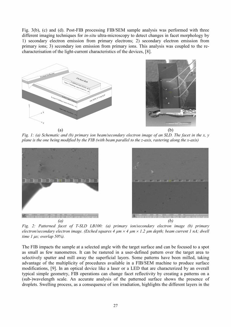
Fig. 3(b), (c) and (d). Post-FIB processing FIB/SEM sample analysis was performed with three
different imaging techniques for in-situ ultra-microscopy to detect changes in facet morphology by
1) secondary electron emission from primary electrons; 2) secondary electron emission from
primary ions; 3) secondary ion emission from primary ions. This analysis was coupled to the re-
characterisation of the light-current characteristics of the devices, [8].
(a) (b)
Fig. 1: (a) Schematic and (b) primary ion beam/secondary electron image of an SLD. The facet in the x, y
plane is the one being modified by the FIB (with beam parallel to the z-axis, rastering along the x-axis)
(a) (b)
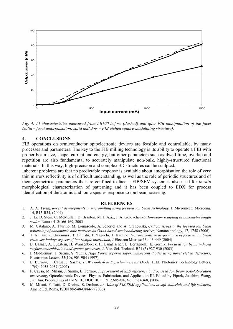
Fig. 2: Patterned facet of T-SLD LB100: (a) primary ion/secondary electron image (b) primary
electron/secondary electron image. (Etched squares 4 µm × 4 µm × 1.2 µm depth; beam current 1 nA; dwell
time 1 µs; overlap 50%).
The FIB impacts the sample at a selected angle with the target surface and can be focused to a spot
as small as few nanometres. It can be rastered in a user-defined pattern over the target area to
selectively sputter and mill away the superficial layers. Some patterns have been milled, taking
advantage of the multiplicity of procedures available in a FIB/SEM machine to produce surface
modifications, [9]. In an optical device like a laser or a LED that are characterized by an overall
typical simple geometry, FIB operations can change facet reflectivity by creating a patterns on a
(sub-)wavelength scale. An accurate analysis of the patterned surface shows the presence of
droplets. Swelling process, as a consequence of ion irradiation, highlights the different layers in the
Z
X
Y
27

device structure by a significantly different response in terms of size and number of droplets that
appear on the inspected surface and rate of secondary electron emission. After FIB manipulation of
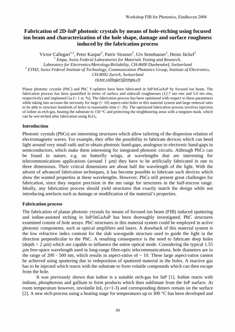
the output facet it is noticed that the output power of the T-SLD is reduced by approximately 35%,
Fig. 4, indicating that the effect of the FIB was to increase facet reflectivity.
(a) (b)
(c) (d)
Fig. 3: (a) Electron image of the facet of LD1200 where Pt-pattern was deposited by FIB on a previously
etched area (beam current 0.1 nA; dwell time 4.2 ms); (b) Electron image of the droplets appearing on the
facet of LB100 (Milled area 4 µm × 4 µm; beam current 0.1 nA; dwell time 0.7 ms; overlap –300; 10
repetitions); (c) Ion image of the droplets generated on LB53 highlighting their distribution and size
dependence on the layer composition (Milled area 8 µm × 20 µm; beam current 1 nA; dwell time 1 µs;
overlap 50%); (d) The same effect observed on LD1200 by electron imaging (beam current 0.1 nA; dwell
time 0.7 ms; overlap –300).
28
0
20
40
60
80
100
0 500 1000 1500
Input current (mA)
Output power (mW)
Fig. 4: LI characteristics measured from LB100 before (dashed) and after FIB manipulation of the facet
(solid – facet amorphisation; solid and dots – FIB etched square-modulating structure).
4. CONCLUSIONS
FIB operations on semiconductor optoelectronic devices are feasible and controllable, by many
processes and parameters. The key to the FIB milling technology is its ability to operate a FIB with
proper beam size, shape, current and energy, but other parameters such as dwell time, overlap and
repetition are also fundamental to accurately manipulate non-bulk, highly-structured functional
materials. In this way, high-precision and complex 3D structures can be sculpted.
Inherent problems are that no predictable response is available about amorphisation the role of very
thin mirrors reflectivity is of difficult understanding, as well as the role of periodic structures and of
their geometrical parameters that are confined to facets. FIB/SEM system is also used for in situ
morphological characterization of patterning and it has been coupled to EDX for process
identification of the atomic and ionic species response to ion beam rastering.
REFERENCES 1. A. A. Tseng, Recent developments in micromilling using focused ion beam technology, J. Micromech. Microeng.
14, R15-R34, (2004)
2. J. Li, D. Stein, C. McMullan, D. Branton, M. J. Aziz, J. A. Golovchenko, Ion-beam sculpting at nanometre length
scales, Nature 412:166-169, 2003
3. M. Catalano, A. Taurino, M. Lomascolo, A. Schertel and A. Orchowski, Critical issues in the focused ion beam
patterning of nanometric hole matrices on GaAs-based semiconducting devices, Nanotechnology, 17, 1758 (2006)
4. T. Ishitani, K. Umemura , T. Ohnishi, T. Yaguchi, T. Kamino, Improvements in performance of focused ion beam
cross-sectioning: aspects of ion-sample interaction, J Electron Microsc 53:443-449 (2004)
5. B. Basnar, A. Lugstein, H. Wanzenboeck, H. Langfischer, E. Bertagnolli, E. Gornik, Focused ion beam induced
surface amorphization and sputter processes, J. Vac. Sci. Technol. B21 (3) 927-930 (2003)
6. I. Middlemast, J. Sarma, S. Yunus, High Power tapered superluminescent diodes using novel etched deflectors,
Electronics Letters, 33(10), 903-904 (1997)
7. L. Burrow, F. Causa, J. Sarma, 1.3W ripple-free Superluminescent Diode, IEEE Photonics Technology Letters,
17(9), 2035-2037 (2005)
8. F. Causa, M. Milani, J. Sarma, L. Ferraro, Improvement of SLD efficiency by Focussed Ion Beam post-fabrication
processing, Optoelectronic Devices: Physics, Fabrication, and Application III. Edited by Piprek, Joachim; Wang,
Jian Jim. Proceedings of the SPIE, DOI: 10.1117/12.685984, Volume 6368, (2006)
9. M. Milani, F. Tatti, D. Drobne, S. Drobne, An Atlas of FIB/SEM applications in soft materials and life sciences,
Aracne Ed, Roma, ISBN 88-548-0884-9 (2006)
29
Fabrication of 2D-InP photonic crystals by means of hole-etching using focused ion beam and characterization of the hole shape, damage and surface roughness
induced by the fabrication process
Victor CallegariP
1,2P, Peter KasparP
2P, Patric StrasserP
2P, Urs SennhauserP
1P, Heinz JäckelP
2P
P
1P Empa, Swiss Federal Laboratories for Materials Testing and Research,
Laboratory for Electronics/Metrology/Reliability, CH-8600 Duebendorf, Switzerland P
2P ETHZ, Swiss Federal Institute of Technology, Communication Photonics Group, Institute of Electronics,
CH-8092 Zurich, Switzerland [email protected] UTH
Planar photonic crystals (PhC) and PhC Y-splitters have been fabricated in InP/InGaAsP by focused ion beam. The fabrication process has been quantified in terms of surface and sidewall roughnesses (12.7 nm rms and 5.0 nm rms, respectively) and implanted Ga (< 1 at. %). The fabrication process has been optimized with respect to these parameters while taking into account the necessity for large (> 10) aspect-ratio holes in this material system and large removal rates to be able to structure hundreds of holes in reasonable time (< 2h). The optimized fabrication process involves injection of iodine as etch-gas, heating the substrate to 150 °C and protecting the neighbouring areas with a tungsten mask, which can be wet-etched after fabrication using HB2BOB2B.
Introduction Photonic crystals (PhCs) are interesting structures which allow tailoring of the dispersion relation of electromagnetic waves. For example, they offer the possibility to fabricate devices which can bend light around very small radii and to obtain photonic band-gaps, analogous to electronic band-gaps in semiconductors, which make them interesting for integrated photonic circuits. Although PhCs can be found in nature, e.g. on butterfly wings, at wavelengths that are interesting for telecommunications applications (around 1 µm) they have to be artificially fabricated in one to three dimensions. Their critical dimensions are about half the wavelength of the light. With the advent of advanced fabrication techniques, it has become possible to fabricate such devices which show the wanted properties at these wavelengths. However, PhCs still present great challenges for fabrication, since they require precision in the nm range for structures in the half-micron range. Ideally, any fabrication process should yield structures that exactly match the design while not introducing artefacts such as damage or modification of the material’s properties.
Fabrication process
The fabrication of planar photonic crystals by means of focused ion beam (FIB) induced sputtering and iodine-assisted etching in InP/InGaAsP has been thoroughly investigated. PhC structures examined consist of hole arrays. PhC structures in this material system could be employed in active photonic components, such as optical amplifiers and lasers. A drawback of this material system is the low refractive index contrast for the slab waveguide structure used to guide the light in the direction perpendicular to the PhC. A resulting consequence is the need to fabricate deep holes (depth > 2 µm) which are capable to influence the entire optical mode. Considering the typical 1.55 µm free-space wavelength used in long-range fibre-optic telecommunications, hole diameters are in the range of 200 - 500 nm, which results in aspect-ratios of ~ 10. These large aspect-ratios cannot be achieved using sputtering due to redeposition of sputtered material in the holes. A reactive gas has to be injected which reacts with the substrate to form volatile compounds which can then escape from the hole.
It was previously shown that iodine is a suitable etch-gas for InP [1]. Iodine reacts with indium, phosphorous and gallium to form products which then sublimate from the InP surface. At room temperature however, involatile InIBx B (x=1-3) and corresponding dimers remain on the surface [2]. A new etch-process using a heating stage for temperatures up to 300 °C has been developed and
30
Workshop FIB for Photonics, Eindhoven 2008
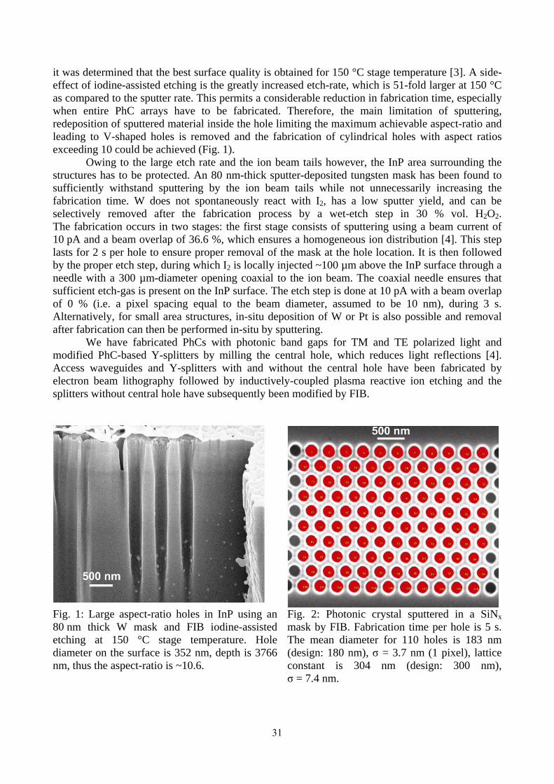
it was determined that the best surface quality is obtained for 150 °C stage temperature [3]. A side-effect of iodine-assisted etching is the greatly increased etch-rate, which is 51-fold larger at 150 °C as compared to the sputter rate. This permits a considerable reduction in fabrication time, especially when entire PhC arrays have to be fabricated. Therefore, the main limitation of sputtering, redeposition of sputtered material inside the hole limiting the maximum achievable aspect-ratio and leading to V-shaped holes is removed and the fabrication of cylindrical holes with aspect ratios exceeding 10 could be achieved (Fig. 1).
Owing to the large etch rate and the ion beam tails however, the InP area surrounding the structures has to be protected. An 80 nm-thick sputter-deposited tungsten mask has been found to sufficiently withstand sputtering by the ion beam tails while not unnecessarily increasing the fabrication time. W does not spontaneously react with IB2 B, has a low sputter yield, and can be selectively removed after the fabrication process by a wet-etch step in 30 % vol. HB2BOB2 B. The fabrication occurs in two stages: the first stage consists of sputtering using a beam current of 10 pA and a beam overlap of 36.6 %, which ensures a homogeneous ion distribution [4]. This step lasts for 2 s per hole to ensure proper removal of the mask at the hole location. It is then followed by the proper etch step, during which IB2B is locally injected ~100 µm above the InP surface through a needle with a 300 µm-diameter opening coaxial to the ion beam. The coaxial needle ensures that sufficient etch-gas is present on the InP surface. The etch step is done at 10 pA with a beam overlap of 0 % (i.e. a pixel spacing equal to the beam diameter, assumed to be 10 nm), during 3 s. Alternatively, for small area structures, in-situ deposition of W or Pt is also possible and removal after fabrication can then be performed in-situ by sputtering.
We have fabricated PhCs with photonic band gaps for TM and TE polarized light and modified PhC-based Y-splitters by milling the central hole, which reduces light reflections [4]. Access waveguides and Y-splitters with and without the central hole have been fabricated by electron beam lithography followed by inductively-coupled plasma reactive ion etching and the splitters without central hole have subsequently been modified by FIB.
Fig. 1: Large aspect-ratio holes in InP using an 80 nm thick W mask and FIB iodine-assisted etching at 150 °C stage temperature. Hole diameter on the surface is 352 nm, depth is 3766 nm, thus the aspect-ratio is ~10.6.
Fig. 2: Photonic crystal sputtered in a SiNBxB mask by FIB. Fabrication time per hole is 5 s. The mean diameter for 110 holes is 183 nm (design: 180 nm), σ = 3.7 nm (1 pixel), lattice constant is 304 nm (design: 300 nm), σ = 7.4 nm.
31

Characterization For the investigated PhCs, the following parameters are important: hole diameter, depth, shape, position, sidewall roughness, and damage to the neighbouring substrate. Hole diameters and positions depend on the beam focus and electronic as well as mechanical drifts. From Fig. 2 the hole diameters and positions for a 1500-hole PhC sputtered at room temperature in a SiNBx B mask without drift compensation during the milling process have been extracted. They were found to not considerably vary, even for fabrication times in the order of 2 hours. The standard deviation for the diameter is one pixel size (3.7 nm), whereas for the position it is 2 pixels, i.e. 7.4 nm. The hole shape is dictated mainly by redeposition and the ion self-focusing effect, which occurs due to ions which are scattered from steep sidewalls and still have enough energy to induce second-order sputtering. This effect can be partly alleviated by choosing a suitable dwell time profile [6].
The influence of the new etching technique has therefore been quantified with respect to the surface and sidewall roughnesses and Ga implantation. The surface and sidewall roughnesses have been measured by atomic force microscopy in contact mode. The surface roughness was found to be 12.7 nm rms after etching at 150 °C, an increase of ~12 nm from the initial polished wafer surface [3]. This increase is mainly due to the large influence of the chemical etch rate and ion intermixing, which is proportional to the ion range. The sidewall roughness was measured from a lamella to be 5.0 nm rms (Fig. 3). The difference between the roughnesses can be explained by the differing ion ranges of 30 keV Ga ions at 0° and grazing angles of incidence, respectively, and thus different intermixing efficiencies.
As a measure of the damage in the substrate, the Ga-implantation was quantified by X-ray photoelectron spectroscopy (XPS) performed at different depths (Fig. 4). It has been found that the Ga contamination was below the detection threshold (<1 at. %) of the XPS system at all depths. This is due on the one hand to the largely increased etch rate and on the other hand to the sublimation of GaIB3 B. Compared to sputtering at room temperature, which results in considerable Ga implantation [2], excessive Ga-implantation could be successfully avoided by etching at 150 °C stage temperature.
Fig. 3: Atomic force microscopy measurement of a lamella etched at 150 °C stage temperature with the identical process used to obtain large aspect-ratio holes. The sidewall roughness is 5.0 nm rms for an area of 500 x 500 nm.
Fig. 4: X-ray photoelectron spectroscopy measurements performed at different depths in the InP substrate previously etched at 150 °C. No Ga is detected. Iodine is present on the surface with a concentration <10 at. %.
32

Optical characterization of PhC Y-splitters The influence of the position of the central hole by FIB has been investigated by measuring the intensity of transmitted light through each branch with an IR camera (Fig. 5). It has been determined from finite-element simulations that the splitting ratio of the two output branches is precisely defined by the position of the central hole [7]. The simulations showed that variations as small as 10 nanometres may lead to ratios that measurably differ from 50 % / 50 %. This method has thus been applied to verify the placement accuracy and reproducibility of the positioning by FIB. It has been found that the FIB positioning accuracy is accurate to within 10 nm, which permits the fabrication of splitters with unity splitting ratio. By intentionally shifting the central hole position, splitting ratios differing from 50 % / 50 % could be achieved (Fig. 5).
Fig. 5: PhC Y-splitter with FIB-etched central holes. The upper part shows a centred hole with the corresponding image obtained by the IR-camera and the line-profile of the light intensity at the centre. The output is equally distributed between the branches. The peak intensity is below the saturation threshold of the camera. The lower part of the image shows a slightly displaced hole and the corresponding intensity distribution of the PhC Y-splitter. The output of the two branches is unequal, with the branch towards which the central hole has been shifted transmitting less light.
Conclusion In conclusion, FIB can provide a single-step method for rapid-prototyping, modification and fabrication of small series of photonic crystal structures in InP/InGaAsP by iodine-assisted etching at 150 °C stage temperature. A prerequisite is the optimization and precise control of the etching parameters, such as the etch gas, gas flux, substrate temperature, beam current and beam overlap. Only when these parameters are optimised can cylindrical holes with aspect-ratios > 10 be reproducibly achieved with reasonable fabrication time, good accuracy and reproducibility.
References [1] A. Yamaguchi and T. Nishikawa, J. Vac. Sci. Technol. B, 13, 962-966, (1995). [2] V. Callegari et al., Appl. Surf. Sci., 253, 8969-8973, (2007). [3] V. Callegari et al., J. Vac. Sci. Technol. B, 25, 2175-2179, (2007). [4] A.A. Tseng, J. Micromech. Microeng., 14, R15-R34, (2004). [5] R. Wilson et al., J. Opt. A: Pure Appl. Opt., 5, S76-S80, (2003). [6] P.M. Nellen et al., Microelectron. Eng., 83, 1805-1808, (2006). [7] P.M. Nellen et al., Microelectron. Eng., 84, 1244-1247, (2007).
33
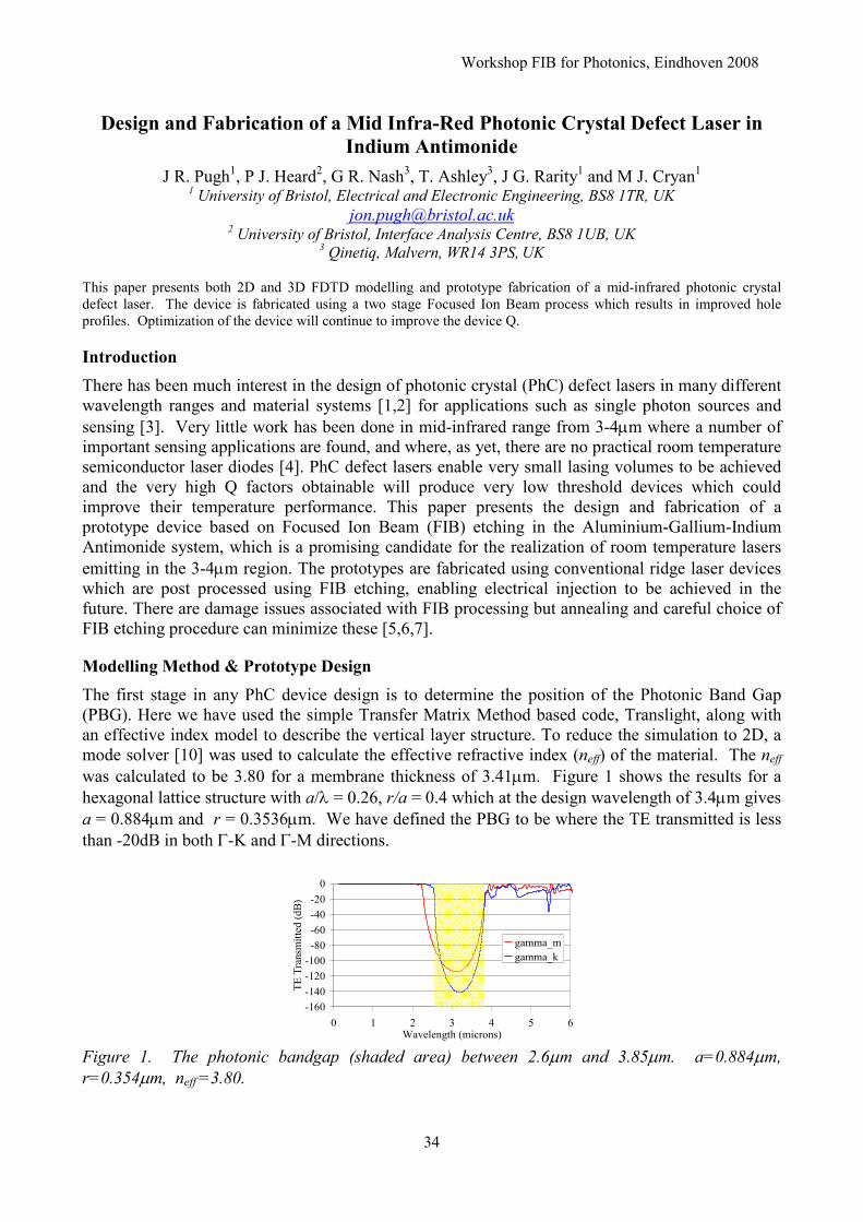
Design and Fabrication of a Mid Infra-Red Photonic Crystal Defect Laser in
Indium Antimonide
J R. Pugh1, P J. Heard
2, G R. Nash
3, T. Ashley
3, J G. Rarity
1 and M J. Cryan
1
1 University of Bristol, Electrical and Electronic Engineering, BS8 1TR, UK
[email protected] 2 University of Bristol, Interface Analysis Centre, BS8 1UB, UK
3 Qinetiq, Malvern, WR14 3PS, UK
This paper presents both 2D and 3D FDTD modelling and prototype fabrication of a mid-infrared photonic crystal
defect laser. The device is fabricated using a two stage Focused Ion Beam process which results in improved hole
profiles. Optimization of the device will continue to improve the device Q.
Introduction
There has been much interest in the design of photonic crystal (PhC) defect lasers in many different
wavelength ranges and material systems [1,2] for applications such as single photon sources and
sensing [3]. Very little work has been done in mid-infrared range from 3-4µm where a number of
important sensing applications are found, and where, as yet, there are no practical room temperature
semiconductor laser diodes [4]. PhC defect lasers enable very small lasing volumes to be achieved
and the very high Q factors obtainable will produce very low threshold devices which could
improve their temperature performance. This paper presents the design and fabrication of a
prototype device based on Focused Ion Beam (FIB) etching in the Aluminium-Gallium-Indium
Antimonide system, which is a promising candidate for the realization of room temperature lasers
emitting in the 3-4µm region. The prototypes are fabricated using conventional ridge laser devices
which are post processed using FIB etching, enabling electrical injection to be achieved in the
future. There are damage issues associated with FIB processing but annealing and careful choice of
FIB etching procedure can minimize these [5,6,7].
Modelling Method & Prototype Design
The first stage in any PhC device design is to determine the position of the Photonic Band Gap
(PBG). Here we have used the simple Transfer Matrix Method based code, Translight, along with
an effective index model to describe the vertical layer structure. To reduce the simulation to 2D, a
mode solver [10] was used to calculate the effective refractive index (neff) of the material. The neff
was calculated to be 3.80 for a membrane thickness of 3.41µm. Figure 1 shows the results for a
hexagonal lattice structure with a/λ = 0.26, r/a = 0.4 which at the design wavelength of 3.4µm gives
a = 0.884µm and r = 0.3536µm. We have defined the PBG to be where the TE transmitted is less
than -20dB in both Γ-K and Γ-M directions.
-160
-140
-120
-100
-80
-60
-40
-20
0
0 1 2 3 4 5 6Wavelength (microns)
TE Transm
itted (dB)
gamma_m
gamma_k
Figure 1. The photonic bandgap (shaded area) between 2.6µm and 3.85µm. a=0.884µm,
r=0.354µm, neff =3.80.
34
Workshop FIB for Photonics, Eindhoven 2008
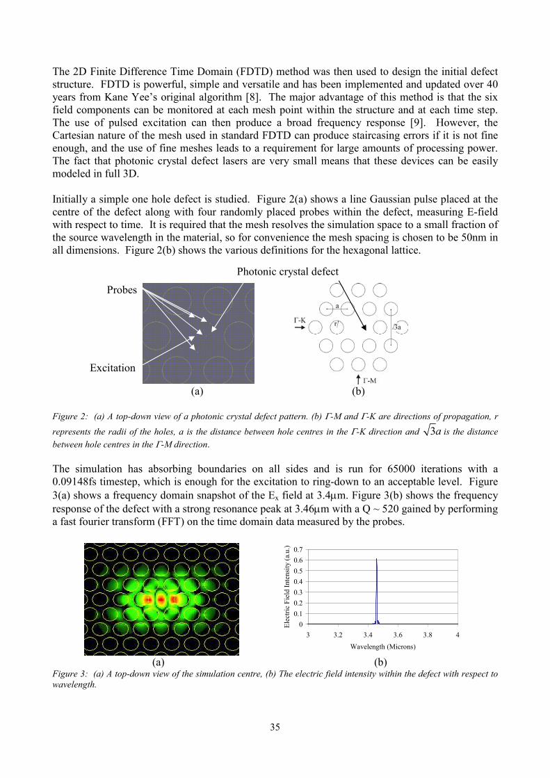
The 2D Finite Difference Time Domain (FDTD) method was then used to design the initial defect
structure. FDTD is powerful, simple and versatile and has been implemented and updated over 40
years from Kane Yee’s original algorithm [8]. The major advantage of this method is that the six
field components can be monitored at each mesh point within the structure and at each time step.
The use of pulsed excitation can then produce a broad frequency response [9]. However, the
Cartesian nature of the mesh used in standard FDTD can produce staircasing errors if it is not fine
enough, and the use of fine meshes leads to a requirement for large amounts of processing power.
The fact that photonic crystal defect lasers are very small means that these devices can be easily
modeled in full 3D.
Initially a simple one hole defect is studied. Figure 2(a) shows a line Gaussian pulse placed at the
centre of the defect along with four randomly placed probes within the defect, measuring E-field
with respect to time. It is required that the mesh resolves the simulation space to a small fraction of
the source wavelength in the material, so for convenience the mesh spacing is chosen to be 50nm in
all dimensions. Figure 2(b) shows the various definitions for the hexagonal lattice.
Figure 2: (a) A top-down view o
represents the radii of the holes,
between hole centres in the Γ-M d
The simulation has absorb
0.09148fs timestep, which i
3(a) shows a frequency dom
response of the defect with a
a fast fourier transform (FFT
(a) Figure 3: (a) A top-down view o
wavelength.
Photonic crystal defect
Probes
Excitation
(
f a p
a is
irec
ing
s en
ain
str
) o
f the
a) (b)
hotonic crystal defect pattern. (b) Γ-M and Γ-K are directions of propagation, r
the distance between hole centres in the Γ-K direction and 3a is the distance
tion.
boundaries on all sides and is run for 65000 iterations with a
ough for the excitation to ring-down to an acceptable level. Figure
snapshot of the Ex field at 3.4µm. Figure 3(b) shows the frequency
ong resonance peak at 3.46µm with a Q ~ 520 gained by performing
n the time domain data measured by the probes.
0
0.1
0.2
0.3
0.4
0.5
0.6
0.7
3 3.2 3.4 3.6 3.8 4
Wavelength (Microns)
Electric Field Intensity (a.u.)
(b)
simulation centre, (b) The electric field intensity within the defect with respect to
35
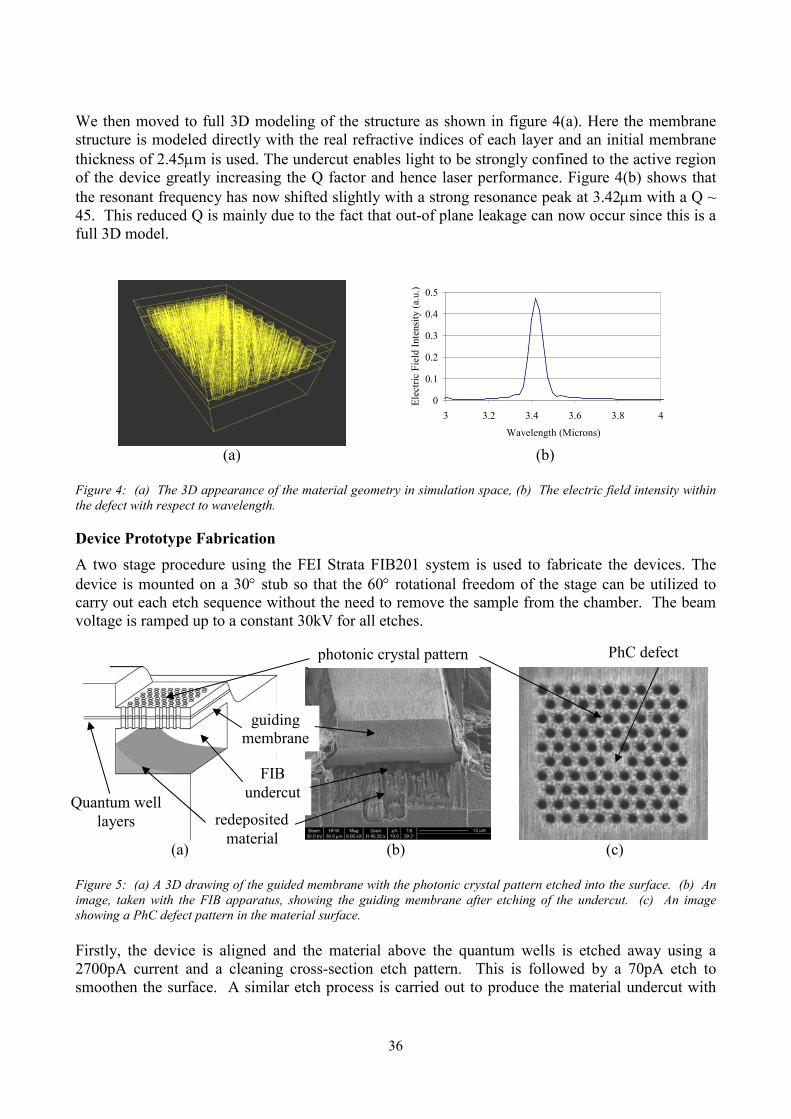
We then moved to full 3D modeling of the structure as shown in figure 4(a). Here the membrane
structure is modeled directly with the real refractive indices of each layer and an initial membrane
thickness of 2.45µm is used. The undercut enables light to be strongly confined to the active region
of the device greatly increasing the Q factor and hence laser performance. Figure 4(b) shows that
the resonant frequency has now shifted slightly with a strong resonance peak at 3.42µm with a Q ~
45. This reduced Q is mainly due to the fact that out-of plane leakage can now occur since this is a
full 3D model.
0
0.1
0.2
0.3
0.4
0.5
3 3.2 3.4 3.6 3.8 4
Wavelength (Microns)
Electric Field Intensity (a.u.)
(a) (b)
Figure 4: (a) The 3D appearance of the material geometry in simulation space, (b) The electric field intensity within
the defect with respect to wavelength.
Device Prototype Fabrication
A two stage procedure using the FEI Strata FIB201 system is used to fabricate the devices. The
device is mounted on a 30° stub so that the 60° rotational freedom of the stage can be utilized to
carry out each etch sequence without the need to remove the sample from the chamber. The beam
voltage is ramped up to a constant 30kV for all etches.
(a) (b)
Figure 5: (a) A 3D drawing of the guided membrane with the photonic crystal pattern etched into
image, taken with the FIB apparatus, showing the guiding membrane after etching of the unde
showing a PhC defect pattern in the material surface.
Firstly, the device is aligned and the material above the quantum wells is etch
2700pA current and a cleaning cross-section etch pattern. This is followed b
smoothen the surface. A similar etch process is carried out to produce the mate
Quantum well
layers
FIB
undercut
redeposited
material
36
PhC defect
photonic crystal patternguiding
membrane
(c)
the surface. (b) An
rcut. (c) An image
ed away using a
y a 70pA etch to
rial undercut with
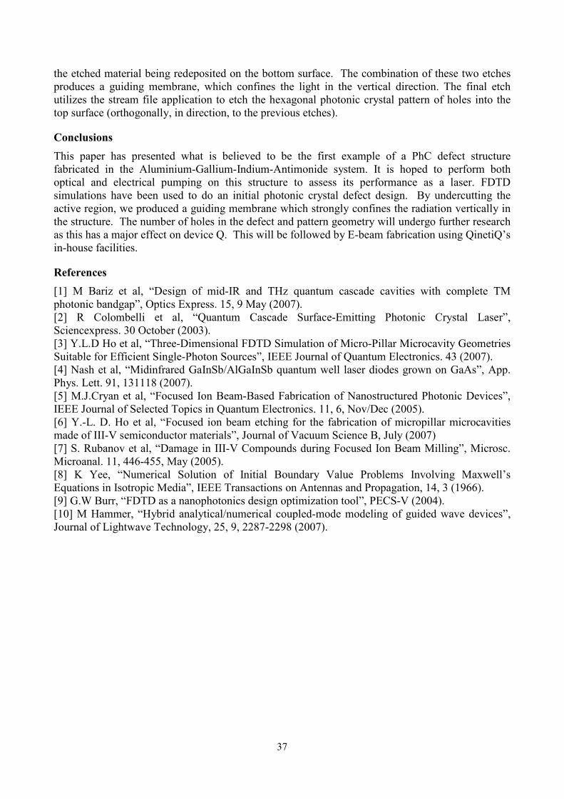
the etched material being redeposited on the bottom surface. The combination of these two etches
produces a guiding membrane, which confines the light in the vertical direction. The final etch
utilizes the stream file application to etch the hexagonal photonic crystal pattern of holes into the
top surface (orthogonally, in direction, to the previous etches).
Conclusions
This paper has presented what is believed to be the first example of a PhC defect structure
fabricated in the Aluminium-Gallium-Indium-Antimonide system. It is hoped to perform both
optical and electrical pumping on this structure to assess its performance as a laser. FDTD
simulations have been used to do an initial photonic crystal defect design. By undercutting the
active region, we produced a guiding membrane which strongly confines the radiation vertically in
the structure. The number of holes in the defect and pattern geometry will undergo further research
as this has a major effect on device Q. This will be followed by E-beam fabrication using QinetiQ’s
in-house facilities.
References
[1] M Bariz et al, “Design of mid-IR and THz quantum cascade cavities with complete TM
photonic bandgap”, Optics Express. 15, 9 May (2007).
[2] R Colombelli et al, “Quantum Cascade Surface-Emitting Photonic Crystal Laser”,
Sciencexpress. 30 October (2003).
[3] Y.L.D Ho et al, “Three-Dimensional FDTD Simulation of Micro-Pillar Microcavity Geometries
Suitable for Efficient Single-Photon Sources”, IEEE Journal of Quantum Electronics. 43 (2007).
[4] Nash et al, “Midinfrared GaInSb/AlGaInSb quantum well laser diodes grown on GaAs”, App.
Phys. Lett. 91, 131118 (2007).
[5] M.J.Cryan et al, “Focused Ion Beam-Based Fabrication of Nanostructured Photonic Devices”,
IEEE Journal of Selected Topics in Quantum Electronics. 11, 6, Nov/Dec (2005).
[6] Y.-L. D. Ho et al, “Focused ion beam etching for the fabrication of micropillar microcavities
made of III-V semiconductor materials”, Journal of Vacuum Science B, July (2007)
[7] S. Rubanov et al, “Damage in III-V Compounds during Focused Ion Beam Milling”, Microsc.
Microanal. 11, 446-455, May (2005).
[8] K Yee, “Numerical Solution of Initial Boundary Value Problems Involving Maxwell’s
Equations in Isotropic Media”, IEEE Transactions on Antennas and Propagation, 14, 3 (1966).
[9] G.W Burr, “FDTD as a nanophotonics design optimization tool”, PECS-V (2004).
[10] M Hammer, “Hybrid analytical/numerical coupled-mode modeling of guided wave devices”,
Journal of Lightwave Technology, 25, 9, 2287-2298 (2007).
37

Focusing diffraction gratings fabricated by FIB for integrated optics applications
Ildar Salakhutdinov, Kalyani Chaganti, Gregory W. Auner
Department of Electrical and Computer Engineering, Wayne State University, Detroit, MI, 48202, USA
Abstract: A sub-micron focusing diffraction grating with 2-D focusing has been designed and fabricated on silicon with focused ion-beam milling. The diffraction grating of size 40 µm by 40 µm focuses He-Ne laser light of wavelength 632.8 nm incident at 75o from the normal to the grating surface at a height of 250 µm to a diffraction limited spot size of about 4 µm. The experimental result matches very well with the expected result from simulation.
1. Introduction Diffractive grating can be used in many integrated optical applications. These applications
include optical disk reading [1], nonlinear integrated optics [2], LED applications [3], and compact integrated topical micro-spectrometer [4]. The challenging part is to minimize the size of integrated topical devices and solution can be with focusing 2-D diffraction gratings [5].
Focusing gratings, in addition to chirp in periodicity, possess curvature of the grooves which together cause two-dimensional focusing of the guided light. E-beam lithography is the most widely-used tool today for the fabrication of two-dimensional gratings [6]. However, e-beam lithography is a multi-step, complex and time-consuming process.
A two-dimensional grating can be fabricated by focused ion-beam milling (FIB), which is a direct-write, single-step process. Even though FIB writing is slower when compared to holographic exposure, it is advantageous since it is a one-step process. Sub-micron patterns can be successfully fabricated on both conducting and non-conducting substrates with FIB technology. Among all substrates, silicon is the most commonly used material for fabrication of structures with FIB. We chose silicon as our substrate for ease of fabrication and designed a two-dimensional grating on it which would focus at a determined height, light of certain wavelength incident at close to grazing angle of incidence. The purpose of this is to closely mimic the scenario of a focusing grating on a thin-film waveguide. This study would give a clear insight not only into the fabrication of sub-micron focusing grating on thin-film waveguides but also into that of sub-micron gratings in general with focused ion-beam milling. Here, we also report the limitations of FIB encountered by us during the fabrication of our two-dimensional focusing grating.
2. Design and fabrication A 40 μm by 40 μm two-dimensional grating was designed to especially focus He-Ne laser
beam (wavelength, λ = 632.8 nm) incident at an angle of 75o from the normal to the grating surface, at a height of 250 μm normally from the center of the grating. The simulation of the grating was done in Matlab considering the focusing grating to be a collection of pixels of size 100nm by 100 nm. Each pixel would be either black or white or in other words, there would be either a peak or a valley at every pixel location. The color of the pixels is determined as follows. The phase P accumulated by light rays emanating from each pixel is calculated as
ba llnP ⋅+⋅=λπ
λπ 22 (1)
38
Workshop FIB for Photonics, Eindhoven 2008
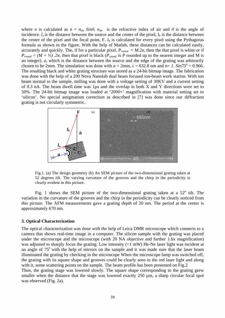
where n is calculated as n = nair Sinθ, nair is the refractive index of air and θ is the angle of incidence. la is the distance between the source and the center of the pixel, lb is the distance between the center of the pixel and the focal point, F. lb is calculated for every pixel using the Pythagoras formula as shown in the figure. With the help of Matlab, these distances can be calculated easily, accurately and quickly. The, if for a particular pixel, Pround = M.2π, then the that pixel is white or if Pround = (M + ½) .2π, then that pixel is black (Pround is P rounded up to the nearest integer and M is an integer). a, which is the distance between the source and the edge of the grating was arbitrarily chosen to be 2mm. The simulation was done with a = 2mm, λ = 632.8 nm and n= 1. Sin75o = 0.966. The resulting black and white grating structure was stored as a 24-bit bitmap image. The fabrication was done with the help of a 200 Nova Nanolab dual beam focused ion-beam work station. With ion beam normal to the sample, milling was done with a voltage setting of 30KV and a current setting of 0.3 nA. The beam dwell time was 1µs and the overlap in both X and Y directions were set to 50%. The 24-bit bitmap image was loaded at ‘2000×’ magnification with material setting set to ‘silicon’. No special astigmatism correction as described in [7] was done since our diffraction grating is not circularly symmetric.
Fig.1. (a) The design geometry (b) An SEM picture of the two-dimensional grating taken at 52 degrees tilt. The varying curvature of the grooves and the chirp in the periodicity is clearly evident in this picture.
Fig. 1 shows the SEM picture of the two-dimensional grating taken at a 52o tilt. The variation in the curvature of the grooves and the chirp in the periodicity can be clearly noticed from this picture. The AFM measurements gave a grating depth of 20 nm. The period at the center is approximately 670 nm.
3. Optical Characterization The optical characterization was done with the help of Leica DMR microscope which connects to a camera that shows real-time image in a computer. The silicon sample with the grating was placed under the microscope and the microscope (with 20 NA objective and further 1.6x magnification) was adjusted to sharply focus the grating. Low intensity (<1 mW) He-Ne laser light was incident at an angle of 75o with the help of mirrors on the sample and it was made sure that the laser beam illuminated the grating by checking in the microscope When the microscope lamp was switched off, the grating with its square shape and grooves could be clearly seen in the red laser light and along with it, some scattering points on the sample. The beam profile has been presented on Fig.2 Then, the grating stage was lowered slowly. The square shape corresponding to the grating grew smaller when the distance that the stage was lowered exactly 250 µm, a sharp circular focal spot was observed (Fig. 2a).
F
lb
C
h
la
40
~ 655nm(a)
a
(b)
39
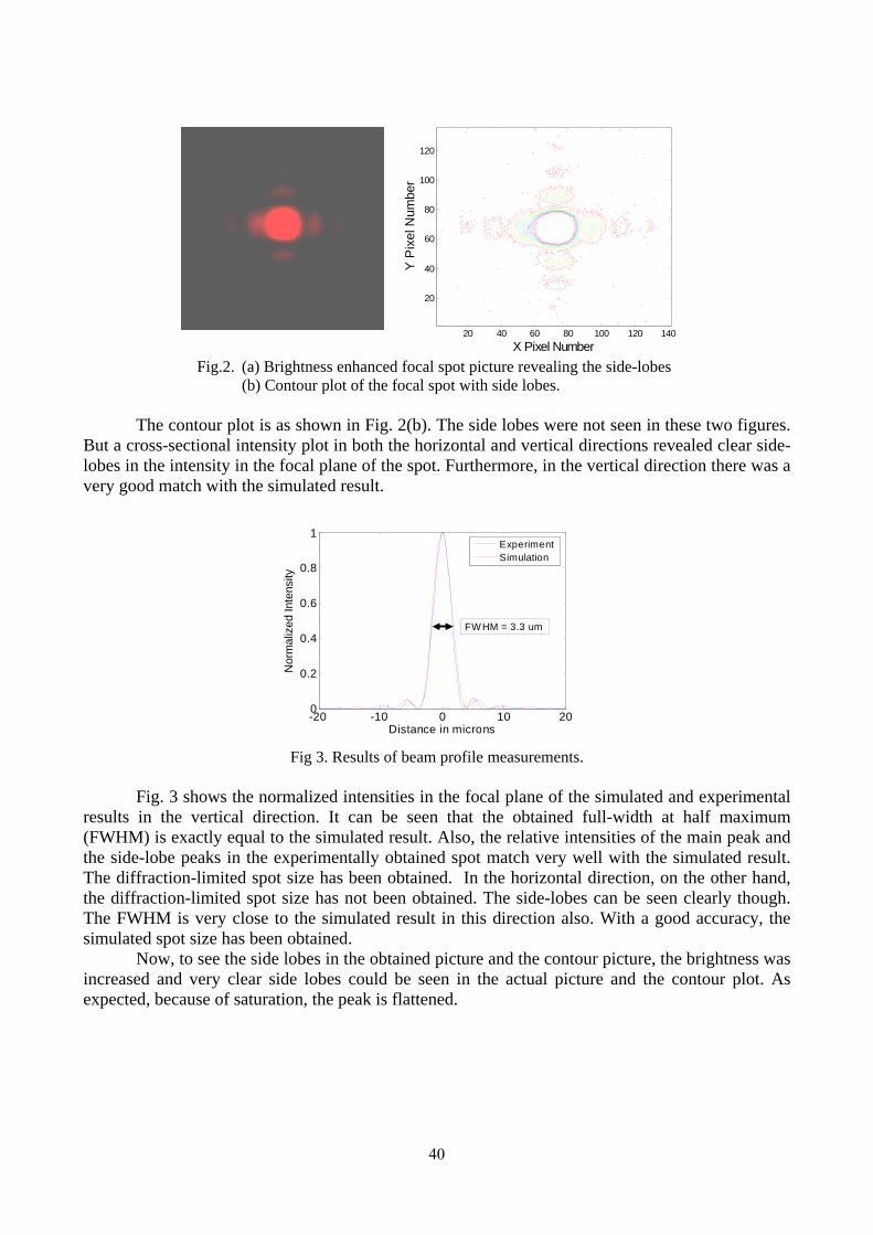
Fig.2. (a) Brightness enhanced focal spot picture revealing the side-lobes (b) Contour plot of the focal spot with side lobes.
The contour plot is as shown in Fig. 2(b). The side lobes were not seen in these two figures.
But a cross-sectional intensity plot in both the horizontal and vertical directions revealed clear side-lobes in the intensity in the focal plane of the spot. Furthermore, in the vertical direction there was a very good match with the simulated result.
Fig 3. Results of beam profile measurements. Fig. 3 shows the normalized intensities in the focal plane of the simulated and experimental
results in the vertical direction. It can be seen that the obtained full-width at half maximum (FWHM) is exactly equal to the simulated result. Also, the relative intensities of the main peak and the side-lobe peaks in the experimentally obtained spot match very well with the simulated result. The diffraction-limited spot size has been obtained. In the horizontal direction, on the other hand, the diffraction-limited spot size has not been obtained. The side-lobes can be seen clearly though. The FWHM is very close to the simulated result in this direction also. With a good accuracy, the simulated spot size has been obtained.
Now, to see the side lobes in the obtained picture and the contour picture, the brightness was increased and very clear side lobes could be seen in the actual picture and the contour plot. As expected, because of saturation, the peak is flattened.
X Pixel Number
Y P
ixel
Num
ber
20 40 60 80 100 120 140
20
40
60
80
100
120
-20 -10 0 10 200
0.2
0.4
0.6
0.8
1
Distance in microns
Nor
mal
ized
Inte
nsity
Experiment Simulation
FW HM = 3.3 um
40

4. Discussion and conclusion Thus, we demonstrated the possibility of fabricating 2-D focused diffraction gratings with FIB. It was shown earlier that FIB can be used for waveguide grating fabrication [8,9]. Thus, this technology can be easily transformed fro integrated optical applications.
We believe also that with FIB, the fabrication procedure becomes much simpler and the goal is to try to achieve a diffractive-limited spot size. Then, it means, the diffraction grating gives an aberration-free performance in the paraxial approximation. For other wavelengths, the performance is yet to be studied.
Acknowledgements This work was supported by U.S. Army TACOM DAAE07-03-C-L140. The authors would like to thank Haiping Sun and Kai Sun of University of Michigan for their help with focused ion-beam milling.
References 1. Ura S., T. Suhara, H. Nishihara, “Aberration characteristics of a focusing grating coupler in an integrated-optic disk
pickup device” Applied Optics, 26, 4777-4782, (1987). 2. Salakhutdinov I.F., Kotačka L., Hoekstra H.J.W.M., Čtyroky J., Sychugov V.A., Parriaux O. “The abnormal
reflecting mirror structure for intra-cavity Čerenkov SHG” Applied Physics B73, 541-545 (2001). 3. Baidus N.V., Salakhutdinov I.F., Hoekstra H.J.W.M., Zvonkov B.N., Nekorkin S.M., Sychugov V.A. “A compact,
tunable, narrow band LD based on emission through the substrate and an external abnormal-reflection mirror” IEEE Photonics Technology Letters, 13, No11, pp.1155-1157 (2001).
4. Chaganti K., Salakhutdinov I., Avrutsky, Auner G.W. “A simple miniature optical spectrometer with a planar waveguide grating coupler in combination with a plano-convex lens” Optics Express, 14, No. 9, 4064-4072 (2006).
5. S. Sheard, T. Liao, G. Yang, P. Prewett and J. Zhu, “Focusing waveguide grating coupler using a diffractive doublet,” Appl. Opt. 36, 4349-4353 (1997).
6. Ura S., T. Suhara, H. Nishihara, “Aberration characteristics of a focusing grating coupler in an integrated-optic disk pickup device” Applied Optics, 26, 4777-4782, (1987).
7. Y. Fu and N.K.A. Bryan, “Influence of astigmatism on the fabrication of diffractive structures by use of focused ion-beam milling,” Opt. Express 12, 3954-3965 (2004)
8. K.E. Zinoviev, C. Dominguez, A. Vila, “Diffraction grating couplers milled in Si3N4 rib waveguides with focused ion beam” Optics Express, 13, No. 21, 8618-8624 (2005).
9. K. Chaganti, I. Salakhutdinov, I. Avrutsky, G. Auner, and J. Mansfield, "Sub-micron grating fabrication on hafnium oxide thin-film waveguides with focused ion-beam milling," Opt. Express 14, 1505-1511 (2006)
41

Focused ion beam milling of three dimensional nanostructures with high precision
R.W. Tjerkstra1, F.B. Segerink2, J.J. Kelly3 and W.L. Vos1,4
1Complex Photonic Systems (COPS), MESA+ Institute for Nanotechnology and Department of Science and
Technology, University of Twente, Enschede. 2Optical Sciences (OS), MESA+ Institute for Nanotechnology and Department of Science and Technology,
University of Twente, Enschede. 3Condensed Matter and Interfaces, Debye Institute, University of Utrecht, Utrecht
4FOM Institute for Atomic and Molecular Physics (AMOLF), Amsterdam.
Abstract The fabrication of an extended three-dimensional nanostructure with dimensions much larger than the feature size using a focused ion beam is described. By milling two identical patterns of pores with a designed diameter of 460 nm in orthogonal directions, a photonic crystal with an inverse woodpile structure was made in a gallium phosphide single crystal. The patterns are aligned with an unprecedented accuracy of 30 nm with respect to each other. The influence of GaP redeposition on the depth, shape, and size of the pores is described. The work is published in J. Vac. Sci. Technol. B [1].
An inverse woodpiles tructure was milled in GaP. We chose GaP because of its high index of refraction and large electronic gap, with a view to eventually making photonic crystals for the visible range. There are few alternative methods to focused ion beam milling in GaP, in contrast to Si, for which many different processing techniques have been developed [2,3]. This makes the study of the milling of GaP with a focused ion beam relevant. The parameters of the inverted woodpile structure that was milled were chosen such that a photonic band gap would, in principle, be centered at wavelengths around 2000 nm. Therefore the diameter D of the pores was 460 nm, and the lattice parameters were a = 958 nm, and c = 677 nm. The thickness of the GaP walls between the pores is only 253 nm. When three-dimensional structures with dimensions that are large compared to their smallest features have to be fabricated, the mutual alignment of the various parts poses a challenge. The orthogonal components are aligned with an accuracy better than 30 nm by using simple
5 mµ
xz
y
Figure 1: Three dimensional inverse woodpile nanostructure made by focused ion beam milling. The x, y, and z axes are indicated.
42
Workshop FIB for Photonics, Eindhoven 2008

alignment marks. This is the first time a nanostructure was made by milling with FIB in two orthogonal directions and aligning the two patters with respect to each other with very high precision using alignment marks. We will call the pores that traverse the slab in the y- direction the y-pores, and the pores that traverse the slab in the z- direction the z-pores. To investigate the influence of porosity on milling, we performed experiments both on bulk wafers and in slabs with a thickness below 2 μm. The diameter of the pores in bulk GaP was designed to be 483 nm. Since the best results were obtained with slabs, we now describe their fabrication. In the first step of the fabrication process a slab was made by milling a large rectangular hole at a distance of about 2 μm from the cleaved edge of the sample. The slab had two faces: the front face, (the cleaved surface of the sample), and the back face, (one of the walls of the rectangular hole). The back face of the slab was smoothened with the “polish mill” option of the focused ion beam apparatus. In this way a slab with the desired thickness of 1.6 to 1.9 μm could be made. After the slab was formed the sample was rotated and the first hole pattern of the structure was milled in the y-direction. Automatic drift correction was applied during milling, using specially milled square markers. In this way a two-dimensional crystal structure of 9 by 9 unit cells with parameters D = 460 nm, a = 958 nm, and c = 677 nm was formed in the slab. In the next step, alignment marks, consisting of two narrow lines with a width of approximately 50 nm and a spacing of 340 nm, were milled in the side of the sample. The sample was again rotated to be able to mill on the top of the slab. Using a cross-shaped alignment mark we aligned the second pattern of pores with respect to the first pattern, and milled it parallel to the front face of the slab, perpendicular to the previously drilled pores, and in the desired places. The diameter of the pores made in bulk material decreased rapidly with depth at the top of the pore, close to the surface of the sample, and more slowly at distances further from the surface (fig. 2, circles). In the slab, however, the diameter of the second set of pores was nearly constant over their whole length. Fig. 2 shows that the average diameter of the z- pores is approximately 300 nm, independant of the distance from the top of the slab. The walls between the pores are 413 nm thick. We observe that the pore diameter is significantly smaller than the designed value of 460 nm. This result is remarkable because the diameter of pores milled in this way is usually slightly larger than the designed diameter, due to beam- and stage drift. Here, stage drift is negligible, and the reduction in the diameter is caused by redeposition during milling.
0 1 2 3 4
1200
1000
800
600
400
200
0
Dia
met
er (n
m)
Depth z ( m)µ
Porous slabBulk
Figure 2: The average diameter of all z- pores in the slab as a function of the depth z inside the pore (connected squares). The average diameter of 5 pores made in bulk material as a function of the depth is shown as connected circles. The tapering of the pores in the slab is much less than that of the pores in bulk material.
43

Fig. 3 shows the final diameter of the y- pores, measured after the z- pores were milled, as a function of the distance z from the top of the wall. The thickness of the redeposited layer inside the pores was calculated on the basis of the initial diameter of the pores (460 nm). The figure clearly shows that the pores located near the top of the wall have the smallest diameter (approximately 30 nm). With increasing depth, the pore diameter increases to approximately 140 nm, which is much smaller than the initial diameter of 460 nm. Fig. 2 shows that the thickness of the redeposited layer in the pores decreases with depth from 220 nm to 160 nm. This result can be explained as follows: when the second set of pores is milled, the y- pores closest to the top of the slab are penetrated first. These y- pores suffer the most from redeposition because they are more exposed to sputtered material during milling. Redeposition of sputtered material during focused ion beam milling of GaP tends to deteriorate the quality of the final structures. Three-dimensional nanostructures were created in single-crystal GaP wafers using focused ion beam milling in two orthogonal directions. A special holder was designed for the process. The two orthogonal patterns of pores were aligned with an accuracy of approximately 30 nm. The highest aspect ratio of pores obtained in bulk GaP was 2.8 ± 0.15, which limits the maximum size of the three dimensional structures. The maximum obtainable aspect ratio in porous material is much larger than 13. References
[1] R.W. Tjerkstra, F.B. Segerink, J.J. Kelly en W.L Vos, J. Vac. Sci. Technol. B. 26, 973-977 (2008)
[2] J. Schilling and A. Scherer, Photonics and Nanostructures - Fundamentals and applications 3, 90 (2005)
[3] L.A. Woldering, R.W. Tjerkstra, H.V. Jansen, I.D. Setija, and W.L. Vos, Nanotechnology 19, 145304: 1-11 (2008)
Distance z from top ( m)µ1 2 3 4 5 6
0
50
100
150
200
250
0
50
100
150
200
250
Dia
met
er (n
m)
Redeposited layer thickness (nm
)
Hole diameterRedeposited layer thickness
Figure 3: Average diameter of the y- pores as a function of their distance z to the top of the porous wall (black squares). The average thickness of the redeposited layers inside the pores is also indicated (red circles).
44

45

Fabrication and characterization of plasmonic nanoresonators using focused-ion-beam-milling
Ernst Jan R. Vesseur, Hans Zeijlemaker and Albert Polman FOM Institute AMOLF, Kruislaan 407, 1098 SJ Amsterdam, The Netherlands
We show how we used focused ion beam (FIB) milling for fabrication of surface plasmon components in a single-crystal Au surface. We used cathodoluminescence (CL) imaging spectroscopy to characterize these structures, which shows confinement of surface plasmons. Moreover, we detected light emission from the sample during FIB fabrication of a plasmonic nanoresonator. The emitted spectrum shows a shift of the resonance as the structure geometry is altered.
Surface plasmons (SPs) are electromagnetic waves that propagate at a metal surface. At
optical frequencies, SPs can carry information at lengths scales below the corresponding optical diffraction limit. If integrated optical components based on SPs could be made, integrated optics at the nanoscale would become a reality.
Focused ion beam milling is an ideal technique to fabricate nanostructured metal surfaces
that carry SPs. Here we show how, by the use of a 30 keV Ga+ ion beam, a single-crystal Au surface is shaped into features that can effectively guide, reflect, confine or outcouple SPs.
Moreover, we characterize the optical properties of our structures during focused ion beam fabrication by detecting light that is emitted from the sample.
A FEI Nova 600 dual-beam workstation was used for
FIB milling. Structures were made in a polished <111> single-crystal Au substrate, grown using the Czochralski process. A 10 pA 30 keV Ga+ beam was scanned over the sample using typically a ~10 nm step size and ~1 μm dwell time. The Ga beam was scanned in rectangular patterns to sputter grooves in the surface, with typical depths and widths in the 100 nm range. Single grooves, groove arrays (gratings), as well as curved grooves and gratings were fabricated. Aside from grooves, also inverse structures were made: rectangular ridges standing out from regions that were sputtered away.
Scanning electron microscopy (SEM) of the ion
milled single-crystal Au shows smooth structures, with high control over the dimensions, and in a very reproducible way. The constant and homogeneous milling rate of single-crystal Au allowed for sub-5 nm depth control.
Cathodoluminescence (CL) imaging spectroscopy was used to study the plasmonic
properties of the ion milled structures. In this technique, a 30 keV electron beam is rastered over the sample, while emitted radiation is collected and dispersed on a CCD array detector. In this setup the electron beam works as a nanoscale SP source, and we detect light emission that is due to outcoupling of SPs. The data show that the structures support distinct resonances that are very sensitive to the fabricated geometry.
Figure 1. Top: a ring groove fabricated in single-crystal Au using focused-ion-beam-milling. The image shows that this substrate allows for reliable and smooth milling. Bottom: cross-section of the ring groove after Pt-deposition, revealing the profile of the grooves.
46
Workshop FIB for Photonics, Eindhoven 2008

In a second experiment, we extended our FIB setup with light detection. By placing a 600-µm core-diameter optical fiber close to the ion and electron beam focus we collect optical radiation emitted under ion and/or electron beam irradiation. The light (spectral range 300-1100 nm), is fiber-guided to a spectrometer equipped with a CCD array for parallel spectral collection, allowing full spectra taken within a second.
We have measured the CL spectrum under 30 keV electron irradiation during 30 keV Ga+ ion beam milling. The CL spectrum serves as a direct probe for the fabricated optical structure during ion milling. We demonstrate this by showing how the CL spectrum of a 300-nm diameter ring-shaped plasmonic nanoresonator fabricated in single-crystal Au shifts by 200 nm by increasing the depth of the ion milled groove.
Our data shows that using focused ion beam milling, single-crystal Au samples can be
accurately milled into structures that support and confine surface plasmons. FIB is therefore an excellent tool for rapid prototyping of nanoscale plasmonic and other optical components.
500 600 700 8000.0
0.2
0.4
0.6
0.8
1.0
1.2
500 nm
Em
issi
on p
roba
bilit
y 10
-3 p
hot.
/ e- /
nm
Wavelength (nm)
Rin
g di
amet
er
100 nm
Figure 2. Cathodoluminescence emission spectra for rings in single-crystal Au with increasing diameter. The spectra show peaks that shift to larger wavelength as the ring diameter increases. Also new peaks appear, showing higher-order resonances.
47
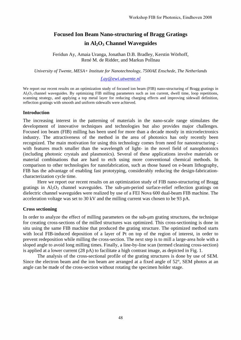
Focused Ion Beam Nano-structuring of Bragg Gratings in Al2O3 Channel Waveguides
Feridun Ay, Amaia Uranga, Jonathan D.B. Bradley, Kerstin Wörhoff, René M. de Ridder, and Markus Pollnau
University of Twente, MESA+ Institute for Nanotechnology, 7500AE Enschede, The Netherlands
We report our recent results on an optimization study of focused ion beam (FIB) nano-structuring of Bragg gratings in Al2O3 channel waveguides. By optimizing FIB milling parameters such as ion current, dwell time, loop repetitions, scanning strategy, and applying a top metal layer for reducing charging effects and improving sidewall definition, reflection gratings with smooth and uniform sidewalls were achieved.
Introduction The increasing interest in the patterning of materials in the nano-scale range stimulates the development of innovative techniques and technologies but also provides major challenges. Focused ion beam (FIB) milling has been used for more than a decade mostly in microelectronics industry. The attractiveness of the method in the area of photonics has only recently been recognized. The main motivation for using this technology comes from need for nanostructuring -with features much smaller than the wavelength of light- in the novel field of nanophotonics (including photonic crystals and plasmonics). Several of these applications involve materials or material combinations that are hard to etch using more conventional chemical methods. In comparison to other technologies for nanofabrication, such as those based on e-beam lithography, FIB has the advantage of enabling fast prototyping, considerably reducing the design-fabrication-characterization cycle time.
Here we report our recent results on an optimization study of FIB nano-structuring of Bragg gratings in Al2O3 channel waveguides. The sub-μm-period surface-relief reflection gratings on dielectric channel waveguides were realized by use of a FEI Nova 600 dual-beam FIB machine. The acceleration voltage was set to 30 kV and the milling current was chosen to be 93 pA.
Cross sectioning In order to analyze the effect of milling parameters on the sub-μm grating structures, the technique for creating cross-sections of the milled structures was optimized. This cross-sectioning is done in situ using the same FIB machine that produced the grating structure. The optimized method starts with local FIB-induced deposition of a layer of Pt on top of the region of interest, in order to prevent redeposition while milling the cross-section. The next step is to mill a large-area hole with a sloped angle to avoid long milling times. Finally, a line-by-line scan (termed cleaning cross-section) is applied at a lower current (28 pA) to facilitate a high contrast image, as depicted in Fig. 1.
The analysis of the cross-sectional profile of the grating structures is done by use of SEM. Since the electron beam and the ion beam are arranged at a fixed angle of 52°, SEM photos at an angle can be made of the cross-section without rotating the specimen holder stage.
48
Workshop FIB for Photonics, Eindhoven 2008

(a) (b) (c)
Pt Pt Al2O3
Fig. 1: Illustration of the cross sectioning procedure: (a) deposition of the Pt layer on top of the grating(top view), (b) milling of a deep sloped hole (top view), (c) final cross-sectional view (at an angle of 52°).
Optimization of the milling process In order to obtain uniform and smooth sidewalls of the grating structures, a study for minimization of the redeposition effects was performed. The dwell time and number of loops were varied while keeping the total dose constant to achieve similar milling depths. In order to avoid charging of the structures a Cr layer with thickness ranging from 10 to 40 nm was sputtered on top. The grating lengths were about 23 μm and waveguides with widths between 2.0 and 3.8 μm were used. The grating period was about 550 nm and the milled depths varied between 150 and 200 nm. The initial thickness of the Al2O3 channel waveguides was about 550 nm [1].
The gratings were realized using a predefined mask file (stream file) that contains milling time, pixel information, and pixel sequence for the desired geometry. The flexibility provided by the stream-file-based patterning allows us to choose the pathway by which the grating is defined on the waveguide. Figure 2(a) shows the cross-section profile of a grating structure obtained with a dwell time of 0.1 ms and 8 loops and in Fig. 2(b) the corresponding profile obtained with a dwell time of 0.001 ms and 800 loops is depicted. The deteriorating effects of redeposition are clearly identified in the first case, dictating that the fabrication process can be optimized by using small dwell times and higher number of loops, thus smoothing out the effects of redeposition. Previous results show that these findings may depend on both, the milled geometry and material used [2].
(a) (b)
Pt Al2O3
Pt Al2O3
Fig. 2: Cross-section profiles of grating structures obtained with (a) a dwell time of 0.1 ms and 8 loops , (b)
a dwell time of 0.001 ms and 800 loops.
49

(a) (b)
Fig. 3: (a) Grating device realized with optimized parameters; (b) cross-sectional profile of the optimized grating structure.
When the scanning is done along a direction perpendicular to the grating grooves, the cross-
sectional profile is distorted due to redeposition effects and the inter-groove space is also milled, resulting in sinking of the entire grating structure. A successful realization of a reflection grating when applying optimized milling parameters is depicted in Fig. 3.
Conclusions By optimizing FIB milling parameters such as ion current, dwell time, loop repetitions, scanning strategy, and applying a top metal layer for reducing charging effects and improving sidewall definition, reflection gratings on Al2O3 channel waveguides with smooth and uniform sidewalls were fabricated.
Acknowledgements This work was supported by the European Union, contract IST-NMP-3-017501 (Photonic Integrated Devices in Activated Amorphous and Crystalline Oxides - PI-OXIDE) and the European Network of Excellence ePIXnet. The authors thank Vishwas Gadgil for his help with operating the FIB machine and Wico Hopman for stimulating discussions.
References [1] J.D.B. Bradley, F. Ay, K. Wörhoff, and M. Pollnau, Appl. Phys. B 89, 311-318 (2007).
[2] W.C.L. Hopman, F. Ay, W. Hu, V.J. Gadgil, L, Kuipers, M, Pollnau, and R.M. de Ridder, Nanotechnol. 18, 195305 (2007).
50

51
Diamond Photonic Crystal: Ultra-high-Q nanocavity FIB assisted fabrication
Igal Bayn1, Boris Meyler
1, Alex Lahav
1, Joseph Salzman
1, Barbara A. Fairchild
2, Steven Prawer
2,
Felix L. Martinez3
1Department of Electrical Engineering and Microelectronics Research Center, Technion Haifa, 32000,
Israel
[email protected] 2Centre for Quantum Computing Technology and Micro Analytical Research Center, School of Physics, The
University of Melbourne 3Department of Electrical Engineering, Polytechnic University of Cartagena
Abstract. We present an ultra-high-Q planar photonic crystal nanocavity fabrication in mono-crystalline diamond. This
fabrication is substantially different from its counterparts, due to extremely high chemical resistance, which makes
standard micro-machining techniques inapplicable. In our processing, the membrane is defined via MeV implantations,
the photonic crystal pattern is FIB milled and the resulting device is relocated onto pre-prepared substrate with Omni-
Probe micromanipulator. Here, we give a detailed description of this process.
Introduction
2D Photonic Crystal Structures in single crystal diamond are being considered as an attractive
architecture for the control and manipulation of atom-photon dressed states [1]. This
implementation requires the capability to couple the optical emission of a single diamond color
center (NV center) to a cavity with a high quality factor (Q) and low mode-volume (Vm). The
photonic crystal (PC) architecture provides integral scalability, which is very important in the
realization of quantum information technology (QIT). Recently, several designs of PC high-Q
cavities on diamond were reported [2-4], while the best cavity is based on the local width
modulation technique [5], exhibiting Q≈1.3×10⁶ and Vm=1.775×(λ/n)
3 [6]. The realization of this
cavity requires precise geometry control over PC-hole's radius, vertical profile, positioning, and
membrane thickness. Due to inherited uncertainty in several critical parameters of diamond
processing, such as membrane thickness, we present here the PC cavities fabrication in a reach NV
center environment designed to be high-Q.
The PC cavity is formed of a membrane suspended in air and periodically modulated by a
triangular array of air holes. The main challenge in diamond-based fabrication is the extreme
chemical resistance of diamond, and the lack of a developed micro-fabrication technology. Here, we
present the manufacturing process of 2D PC devices realized on a mono-crystalline diamond
membrane. The membrane is formed by an ion implantation technique discussed bellow, while the
PC is patterned by FIB milling. The resulting structure is relocated onto a pre-prepared silicon
substrate for further optical characterization. All fabrication processes excluding ion implantation
and essential etching/annealing are performed in situ, in a Strata 400 STEM Dual Beam machine
(FEI). We are not aware of any previous report of mono-crystalline diamond photonic crystal
fabrication.
Membrane Fabrication
The membrane thickness required for a slab PC is ~200 nm. The fabrication of this membrane in
bulk diamond is a technological challenge. Most of existing techniques in diamond micromachining
are based on chemical vapor deposition (CVD) of polycrystalline films with subsequent ablation
process. This polycrystalline diamond has a poor optical transparency and high scattering [7], thus
unsuitable for the PCs. Here, the membrane is fabricated in a single crystalline diamond (Type Ib)
of Sumitomo.
The thin diamond membrane is formed by two consecutive implantations of a high dose of
He+ ions at energies of 2MeV and 1.8MeV. These implantations produce lattice defects, resulting
52
Workshop FIB for Photonics, Eindhoven 2008
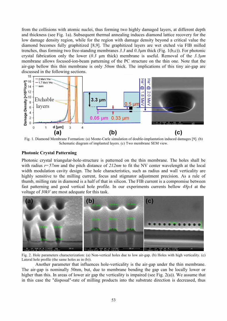
from the collisions with atomic nuclei, thus forming two highly damaged layers, at different depth
and thickness (see Fig. 1a). Subsequent thermal annealing induces diamond lattice recovery for the
low damage density region, while for the region with damage density beyond a critical value the
diamond becomes fully graphitized [8,9]. The graphitized layers are wet etched via FIB milled
trenches, thus forming two free-standing membranes 3.3 and 0.3µm thick (Fig. 1(b,c)). For photonic
crystal fabrication only the lower (0.3 µm thick) membrane is useful. Removal of the 3.3µm
membrane allows focused-ion-beam patterning of the PC structure on the thin one. Note that the
air-gap bellow this thin membrane is only 50nm thick. The implications of this tiny air-gap are
discussed in the following sections.
Fig. 1. Diamond Membrane Formation: (a) Monte-Carle simulation of double-implantation induced damages [9]. (b)
Schematic diagram of implanted layers. (c) Two membrane SEM view.
Photonic Crystal Patterning
Photonic crystal triangular-hole-structure is patterned on the thin membrane. The holes shall be
with radius r=57nm and the pitch distance of 212nm to fit the NV center wavelength at the local
width modulation cavity design. The hole characteristics, such as radius and wall verticality are
highly sensitive to the milling current, focus and stigmator adjustment precision. As a rule of
thumb, milling rate in diamond is a half of that in silicon. The FIB current is a compromise between
fast patterning and good vertical hole profile. In our experiments currents bellow 48pA at the
voltage of 30kV are most adequate for this task.
Fig. 2. Hole parameters characterization: (a) Non-vertical holes due to low air-gap. (b) Holes with high verticality. (c)
Lateral hole profile (the same holes as in (b)).
Another parameter that influences hole-verticality is the air-gap under the thin membrane.
The air-gap is nominally 50nm, but, due to membrane bending the gap can be locally lower or
higher than this. In areas of lower air gap the verticality is impaired (see Fig. 2(a)). We assume that
in this case the "disposal"-rate of milling products into the substrate direction is decreased, thus
53
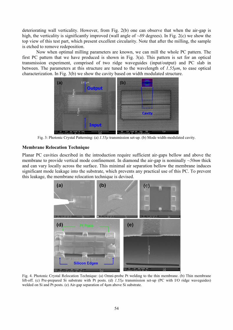
deteriorating wall verticality. However, from Fig. 2(b) one can observe that when the air-gap is
high, the verticality is significantly improved (wall angle of ~89 degrees). In Fig. 2(c) we show the
top view of this test part, which present excellent circularity. Note that after the milling, the sample
is etched to remove redeposition.
Now when optimal milling parameters are known, we can mill the whole PC pattern. The
first PC pattern that we have produced is shown in Fig. 3(a). This pattern is set for an optical
transmission experiment, comprised of two ridge waveguides (input/output) and PC slab in
between. The parameters at this structure are tuned to the wavelength of 1.55µm, to ease optical
characterization. In Fig. 3(b) we show the cavity based on width modulated structure.
Fig. 3: Photonic Crystal Patterning: (a) 1.55µ transmission set-up. (b) Mode width-modulated cavity.
Membrane Relocation Technique
Planar PC cavities described in the introduction require sufficient air-gaps bellow and above the
membrane to provide vertical mode confinement. In diamond the air-gap is nominally ~50nm thick
and can vary locally across the surface. This minimal air separation bellow the membrane induces
significant mode leakage into the substrate, which prevents any practical use of this PC. To prevent
this leakage, the membrane relocation technique is devised.
Fig. 4. Photonic Crystal Relocation Technique: (a) Omni-probe Pt welding to the thin membrane. (b) Thin membrane
lift-off. (c) Pre-prepared Si substrate with Pt posts. (d) 1.55µ transmission set-up (PC with I/O ridge waveguides)
welded on Si and Pt posts. (e) Air-gap separation of 4µm above Si substrate.
54
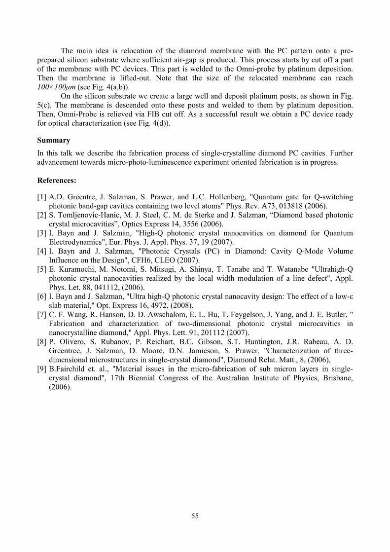
The main idea is relocation of the diamond membrane with the PC pattern onto a pre-
prepared silicon substrate where sufficient air-gap is produced. This process starts by cut off a part
of the membrane with PC devices. This part is welded to the Omni-probe by platinum deposition.
Then the membrane is lifted-out. Note that the size of the relocated membrane can reach
100×100µm (see Fig. 4(a,b)).
On the silicon substrate we create a large well and deposit platinum posts, as shown in Fig.
5(c). The membrane is descended onto these posts and welded to them by platinum deposition.
Then, Omni-Probe is relieved via FIB cut off. As a successful result we obtain a PC device ready
for optical characterization (see Fig. 4(d)).
Summary
In this talk we describe the fabrication process of single-crystalline diamond PC cavities. Further
advancement towards micro-photo-luminescence experiment oriented fabrication is in progress.
References:
[1] A.D. Greentre, J. Salzman, S. Prawer, and L.C. Hollenberg, "Quantum gate for Q-switching
photonic band-gap cavities containing two level atoms" Phys. Rev. A73, 013818 (2006).
[2] S. Tomljenovic-Hanic, M. J. Steel, C. M. de Sterke and J. Salzman, “Diamond based photonic
crystal microcavities”, Optics Express 14, 3556 (2006).
[3] I. Bayn and J. Salzman, "High-Q photonic crystal nanocavities on diamond for Quantum
Electrodynamics", Eur. Phys. J. Appl. Phys. 37, 19 (2007).
[4] I. Bayn and J. Salzman, "Photonic Crystals (PC) in Diamond: Cavity Q-Mode Volume
Influence on the Design", CFH6, CLEO (2007).
[5] E. Kuramochi, M. Notomi, S. Mitsugi, A. Shinya, T. Tanabe and T. Watanabe "Ultrahigh-Q
photonic crystal nanocavities realized by the local width modulation of a line defect", Appl.
Phys. Let. 88, 041112, (2006).
[6] I. Bayn and J. Salzman, "Ultra high-Q photonic crystal nanocavity design: The effect of a low-ε
slab material," Opt. Express 16, 4972, (2008).
[7] C. F. Wang, R. Hanson, D. D. Awschalom, E. L. Hu, T. Feygelson, J. Yang, and J. E. Butler, "
Fabrication and characterization of two-dimensional photonic crystal microcavities in
nanocrystalline diamond," Appl. Phys. Lett. 91, 201112 (2007).
[8] P. Olivero, S. Rubanov, P. Reichart, B.C. Gibson, S.T. Huntington, J.R. Rabeau, A. D.
Greentree, J. Salzman, D. Moore, D.N. Jamieson, S. Prawer, "Characterization of three-
dimensional microstructures in single-crystal diamond", Diamond Relat. Matt., 8, (2006),
[9] B.Fairchild et. al., "Material issues in the micro-fabrication of sub micron layers in single-
crystal diamond", 17th Biennial Congress of the Australian Institute of Physics, Brisbane,
(2006).
55
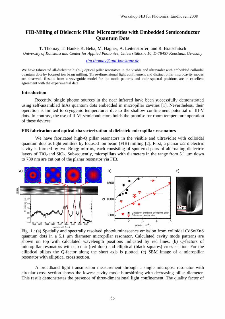
FIB-Milling of Dielectric Pillar Microcavities with Embedded Semiconductor Quantum Dots
T. Thomay, T. Hanke, K. Beha, M. Hagner, A. Leitenstorfer, and R. Bratschitsch University of Konstanz and Center for Applied Photonics, Universitätsstr. 10, D-78457 Konstanz, Germany
We have fabricated all-dielectric high-Q optical pillar resonators in the visible and ultraviolet with embedded colloidal quantum dots by focused ion beam milling. Three-dimensional light confinement and distinct pillar microcavity modes are observed. Results from a waveguide model for the mode patterns and their spectral positions are in excellent agreement with the experimental data
Introduction Recently, single photon sources in the near infrared have been successfully demonstrated
using self-assembled InAs quantum dots embedded in micropillar cavities [1]. Nevertheless, their operation is limited to cryogenic temperatures due to the shallow confinement potential of III-V dots. In contrast, the use of II-VI semiconductors holds the promise for room temperature operation of these devices.
FIB fabrication and optical characterization of dielectric micropillar resonators
We have fabricated high-Q pillar resonators in the visible and ultraviolet with colloidal quantum dots as light emitters by focused ion beam (FIB) milling [2]. First, a planar λ/2 dielectric cavity is formed by two Bragg mirrors, each consisting of sputtered pairs of alternating dielectric layers of TiO2 and SiO2. Subsequently, micropillars with diameters in the range from 5.1 µm down to 780 nm are cut out of the planar resonator via FIB.
Fig. 1.: (a) Spatially and spectrally resolved photoluminescence emission from colloidal CdSe/ZnS quantum dots in a 5.1 µm diameter micropillar resonator. Calculated cavity mode patterns are shown on top with calculated wavelength positions indicated by red lines. (b) Q-factors of micropillar resonators with circular (red dots) and elliptical (black squares) cross section. For the elliptical pillars the Q-factor along the short axis is plotted. (c) SEM image of a micropillar resonator with elliptical cross section.
A broadband light transmission measurement through a single micropost resonator with
circular cross section shows the lowest cavity mode blueshifting with decreasing pillar diameter. This result demonstrates the presence of three-dimensional light confinement. The quality factor of
634 636 638 640 642 644 646 648 65020
30
40
50
60
70
80 PL Intensity
!exc: 532 nmTint = 1500 sI = 400 W/cm2
PL in
tensit
y (a.u
.)
wavelength (nm)
1.91 1.92 1.93 1.94 1.95
energy (eV)
a) b) c)
56
Workshop FIB for Photonics, Eindhoven 2008

the cavity is identical to the value for the planar resonator in case of the 2.4 µm pillar and linearly deteriorates with smaller diameters due to light scattering at the sidewalls of the microresonator. In the photoluminescence emission from a quantum dot ensemble located in the spacer layer, higher cavity modes are clearly visible (Figure 1a). The spectral position of these resonances may be calculated by modeling the micropillar resonator as a waveguide with an effective refractive index. As can be seen in Figure 1a, the theoretical results are in excellent agreement with the experimentally observed pillar mode patterns and frequencies.
Via FIB milling, we have also fabricated micropost resonators with elliptical cross section (Fig. 1c). This shape results in linearly polarized photoluminescence emission from the cavity. We find a systematically higher Q-factor for light polarization along the short axis of the elliptical pillar compared to circular ones (Fig. 1b). This result is different to reports on micropost resonators based on the III-V material system, where the Q-factor in direction of the long axis is favorable.
Fig. 2. (a) SEM image of a coupled pillar microcavity (“photonic molecule”) with embedded colloidal CdSe/ZnSe quantum dots, (b) SEM image of a 3x3 coupled pillar microcavity array.
Figure 2 shows that it is possible to fabricate via FIB-milling even more complex structures of coupled microcavities. Light emission from a ‘photonic molecule’ (Fig. 2a) consists of coupled modes of the two cylindrical pillars. Even more complex structures interesting for quantum information processing such as a microcavity array can be easily milled with the FIB (Fig. 2b).
Extending the pillar microcavity concept to the ultraviolet, we have fabricated the first high-quality dielectric pillar microcavities with embedded colloidal ZnO quantum dots. For low-loss mirrors we use HfO2/SiO2 layer pairs for the Bragg mirrors. Cylindrically-shaped pillars with diameters ranging from 600 nm up to 3.2 µm were milled out of the planar cavity. The photoluminescence emission from a single pillar resonator shows a series of distinct cavity modes in the ultraviolet, indicating three-dimensional light-confinement. The spectral positions and spatial patterns of the pillar modes derived by modelling the pillar cavity as a waveguide with an effective refractive index are in excellent agreement with the experiment.
Conclusions
In summary, we have fabricated high-Q micropillar cavities in the visible and ultraviolet containing colloidal quantum dots in the spacer layer via FIB milling. We find a systematically higher Q-factor along the short axis of the elliptical pillar compared to circular ones. The spectral
a) b)
57

position of the cavity resonances have been calculated by modeling the pillar cavity as a waveguide with an effective refractive index. Theoretical results are in excellent agreement with the experimentally determined mode positions.
References [1] Y. Yamamoto, C. Santori, G. Solomon, J. Vuckovic, D. Fattal, E. Waks, and E. Diamanti, Progress in Informatics, 1, 5 (2005). [2] M. Kahl, T. Thomay, V. Kohnle, K. Beha, J. Merlein, M. Hagner, A. Halm, J. Ziegler, T. Nann, Y Fedutik, U. Woggon, M. Artemyev, F. Pérez-Willard, A. Leitenstorfer, and R. Bratschitsch, Nano Lett. 7(9), 2897 (2007).
58

59

Author index
Abram, I ..............................2 Aigouy, L ............................2 Ashley, T...........................34 Auner, GW........................38 Ay, F .....................III, 12, 48
Baets, R...............................4 Bauerdick, S........................2 Bayn, I...............................52 Beha, K .............................56 Benchabane, S...................16 Bernal, M-P.......................16 Beveratos, A........................2 Bourhis, E ...........................2 Bradley, JDB ....................48 Braive, R .............................2 Bratschitsch, R ..................56 Bruchhaus, L.......................2
Callegari, V.......................30 Causa, F ............................26 Chaganti, K .......................38 Colombelli, R......................2 Courjal, N..........................16 Cryan, MJ..........................34
Dahdah, J ..........................16 de Ridder, RM.......III, 12, 48
Fairchild, BA ...................52 Ferraro, L ..........................26
Gierak, J ..............................2
Hagner, M .........................56 Hanke, T............................56 Heard, PJ...........................34 Hobler, G ............................8 Hopman, WCL..................12
Jäckel, H............................30 Jede, R.................................2
Kaspar, P...........................30 Kauppinen, L.J..................III Kelly, JJ ............................42 Kim, H-B ............................8
Lahav, A ........................... 52 Laurent, S ........................... 2 Leitenstorfer, A................. 56
Mailly, D............................. 2 Martinez, FL ..................... 52 Meyler, B.......................... 52 Milani, M.......................... 26
Nash, GR .......................... 34
Pollnau, M ........................ 48 Polman, A ......................... 46 Prawer, S........................... 52 Pugh, JR............................ 34
Qiu, M............................... 22
Rarity, JG.......................... 34 Robert Philip, I ................... 2
Sagnes, I ............................. 2 Salakhutdinov, I................ 38 Salut, R ............................. 16 Salzman, J......................... 52 Sarma, J ............................ 26 Schrauwen, J....................... 4 Segerink, FB ..................... 42 Sennhauser, U................... 30 Spajer, M .......................... 16 Strasser, P ......................... 30
Tatti, F .............................. 26 Thomay, T ........................ 56 Tian, J ............................... 22 Tjerkstra, RW ................... 42
Ulliac, G ........................... 16 Uranga, A ......................... 48
Van Lysebettens, J.............. 4 Van Thourhout, D............... 4 Vanhoutte, M...................... 4 Vesseur, EJR..................... 46 Vos, WL ........................... 42
Wörhoff, K ....................... 48
Zeijlemaker, H.................. 46

ISBN: 978-90-365-2678-4
University of TwenteEnschede, The NetherlandsJune 2008
Supported by