Crystal defect (Imperfection)
11
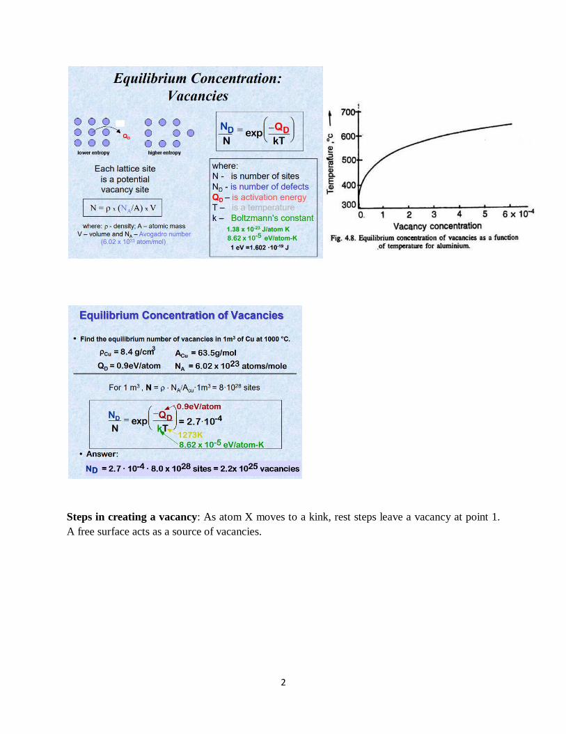
1 Crystal defect (Imperfection) Is imperfection in the regular geometrical arrangement of the atoms in a crystalline solid. These imperfections result from deformation of the solid by: rapid cooling from high temperature, or high-energy radiation (X-rays or neutrons) striking the solid, foreign atoms, external stresses, thermal effect. These defects influence its mechanical, electrical, and optical behavior. Defects included: Point defects, linear defects , surface defects I) Point defects: vacancy types, Frenkel type, the Schottky type, and the impurity type. A point defect is a very localised disruption in the regularity of a lattice. It is a defect of dimensions just like a point (zero dimensions). The size of the defect could be one atom, or two atomic diameters, which is just like a point. A point defect extends its influence only a few atomic diameters beyond its lattice position. 1. Vacancy: When an atom is missing from its lattice site in a crystal structure, it is called a vacancy (or vacant lattice site). The atoms surrounding a vacancy experience a slight displacement into the empty lattice site, and thus, a vacancy is a centre of approximately spherical distortion in the lattice. There could be di-vacancies (an association of two vacancies) or even tri-vacancies. The vacancies equilibrium concentration increases (exponentially) with the increase of temperature
-
Upload
khangminh22 -
Category
Documents
-
view
0 -
download
0
Transcript of Crystal defect (Imperfection)

1
Crystal defect (Imperfection)
Is imperfection in the regular geometrical arrangement of the atoms in a crystalline solid.
These imperfections result from deformation of the solid by:
rapid cooling from high temperature, or high-energy radiation (X-rays or neutrons) striking the
solid, foreign atoms, external stresses, thermal effect.
These defects influence its mechanical, electrical, and optical behavior.
Defects included: Point defects, linear defects , surface defects
I) Point defects: vacancy types, Frenkel type, the Schottky type, and the impurity type. A
point defect is a very localised disruption in the regularity of a lattice. It is a defect of dimensions
just like a point (zero dimensions). The size of the defect could be one atom, or two atomic
diameters, which is just like a point. A point defect extends its influence only a few atomic
diameters beyond its lattice position.
1. Vacancy:
When an atom is missing from its lattice site in a crystal structure, it is called a vacancy (or
vacant lattice site). The atoms surrounding a vacancy experience a slight displacement into the
empty lattice site, and thus, a vacancy is a centre of approximately spherical distortion in the
lattice.
There could be di-vacancies (an association of two vacancies) or even tri-vacancies. The
vacancies equilibrium concentration increases (exponentially) with the increase of temperature
2
Steps in creating a vacancy: As atom X moves to a kink, rest steps leave a vacancy at point 1.
A free surface acts as a source of vacancies.

3
The creation of vacancies becomes easier with the increase of temperature as thermal energy
helps in the diffusion of the atoms.
Vacancies play an important role in the diffusion of atoms in common industrial processes like:
annealing, precipitation hardening, sintering, surface hardening, oxidation and creep of metals.
The number of vacancies can become more than their equilibrium concentration one of the
reasons:
1. A solid hot metal after fast quenching retains the vacancies.
2. Cold working creates vacancies particularly at jogs.
3. Oxidation of some metals such as Cu, Ni, Zn, etc. causes lattice vacancies.
2.Interstitially (Self-Interstitial):
an atom occupies an interstitial site (which is not its normal site), Normally, it requires large
energy to create an interstitially. The size of an interstitial site is very small, particularly in
close-packed crystal structures are much more elastically strained (displaced) than around a
vacancy.
Conditions makes vacancis: exposure to high energy neutrons in a nuclear reactor, or by drastic
cold working.
4
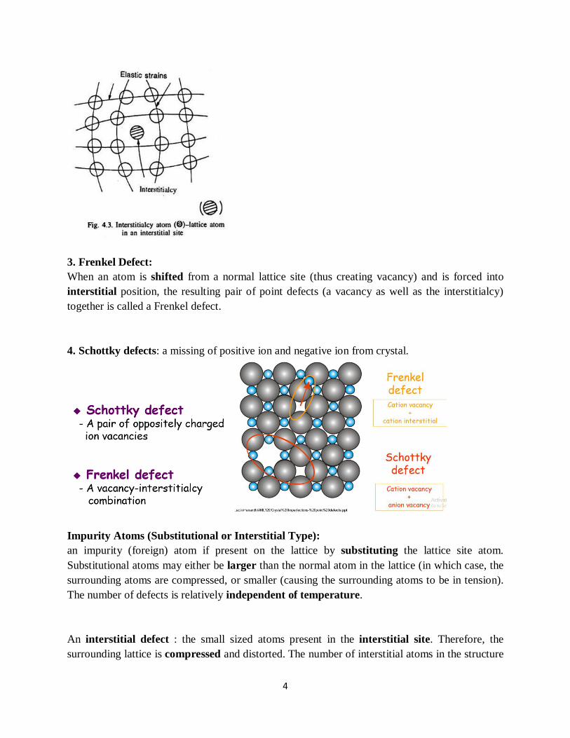
3. Frenkel Defect:
When an atom is shifted from a normal lattice site (thus creating vacancy) and is forced into
interstitial position, the resulting pair of point defects (a vacancy as well as the interstitialcy)
together is called a Frenkel defect.
4. Schottky defects: a missing of positive ion and negative ion from crystal.
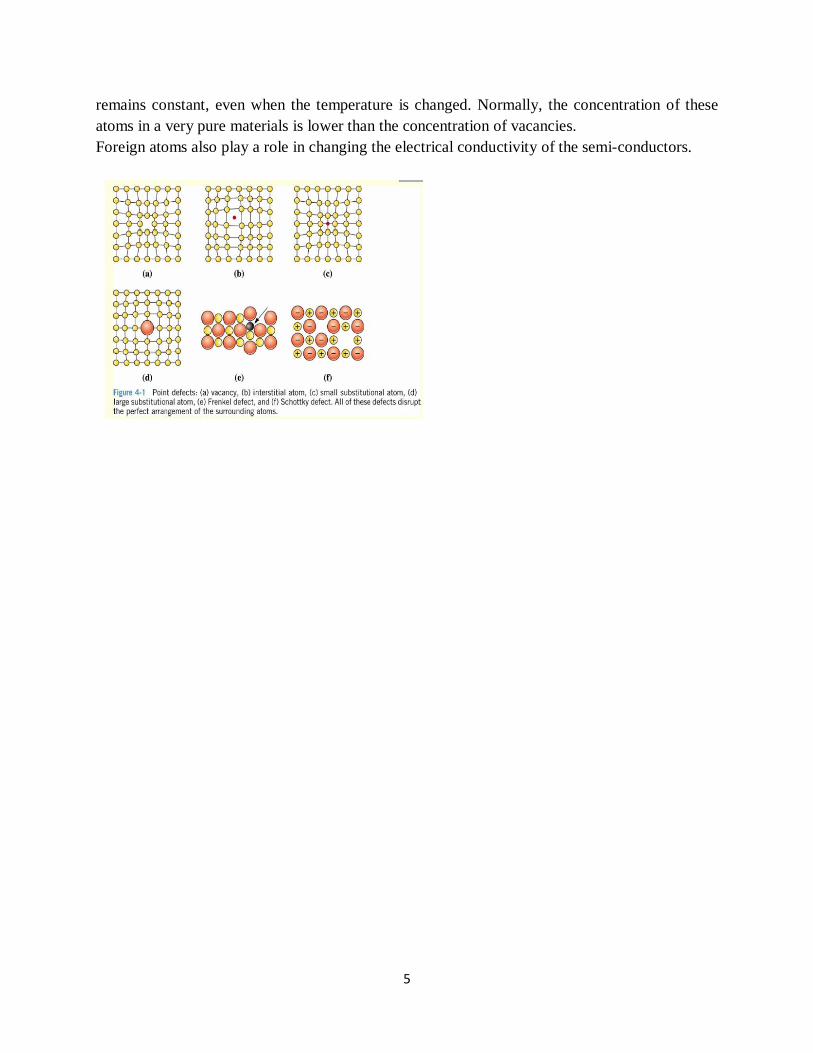
Impurity Atoms (Substitutional or Interstitial Type):
an impurity (foreign) atom if present on the lattice by substituting the lattice site atom.
Substitutional atoms may either be larger than the normal atom in the lattice (in which case, the
surrounding atoms are compressed, or smaller (causing the surrounding atoms to be in tension).
The number of defects is relatively independent of temperature.
An interstitial defect : the small sized atoms present in the interstitial site. Therefore, the
surrounding lattice is compressed and distorted. The number of interstitial atoms in the structure
5
remains constant, even when the temperature is changed. Normally, the concentration of these
atoms in a very pure materials is lower than the concentration of vacancies.
Foreign atoms also play a role in changing the electrical conductivity of the semi-conductors.

6
II) Linear Defects – Dislocations
Line defects, or dislocations, are lines along which whole rows of atoms in a solid are arranged
anomalously. The resulting irregularity in spacing is most severe along a line called the line of
dislocation. Line defects can weaken or strengthen solids. Dislocations are generated and move
when a stress is applied. The motion of dislocations allows slip – plastic deformation to occur.
There are two basic types of dislocations: the edge dislocation and the screw dislocation.
Edge Dislocations
Edge dislocations occur when an extra half -plane is inserted. The slip plane is at the end of the
plane. This line runs along the top of the extra half-plane. The inter-atomic bonds are
significantly distorted only in the immediate around of the dislocation line.
the dislocation moves similarly moves a small amount at a time. The dislocation in the top half
of the crystal is slipping one plane at a time as it moves to the right from its position in image (a)
to its position in image (b) and finally image (c). In the process of slipping one plane at a time
the dislocation propagates across the crystal. The movement of the dislocation across the plane
eventually causes the top half of the crystal to move with respect to the bottom half. However,
only a small fraction of the bonds are broken at any given time. Movement in this manner
requires a much smaller force than breaking all the bonds across the middle plane
simultaneously. the edge dislocation moves parallel to the direction of stress.
7
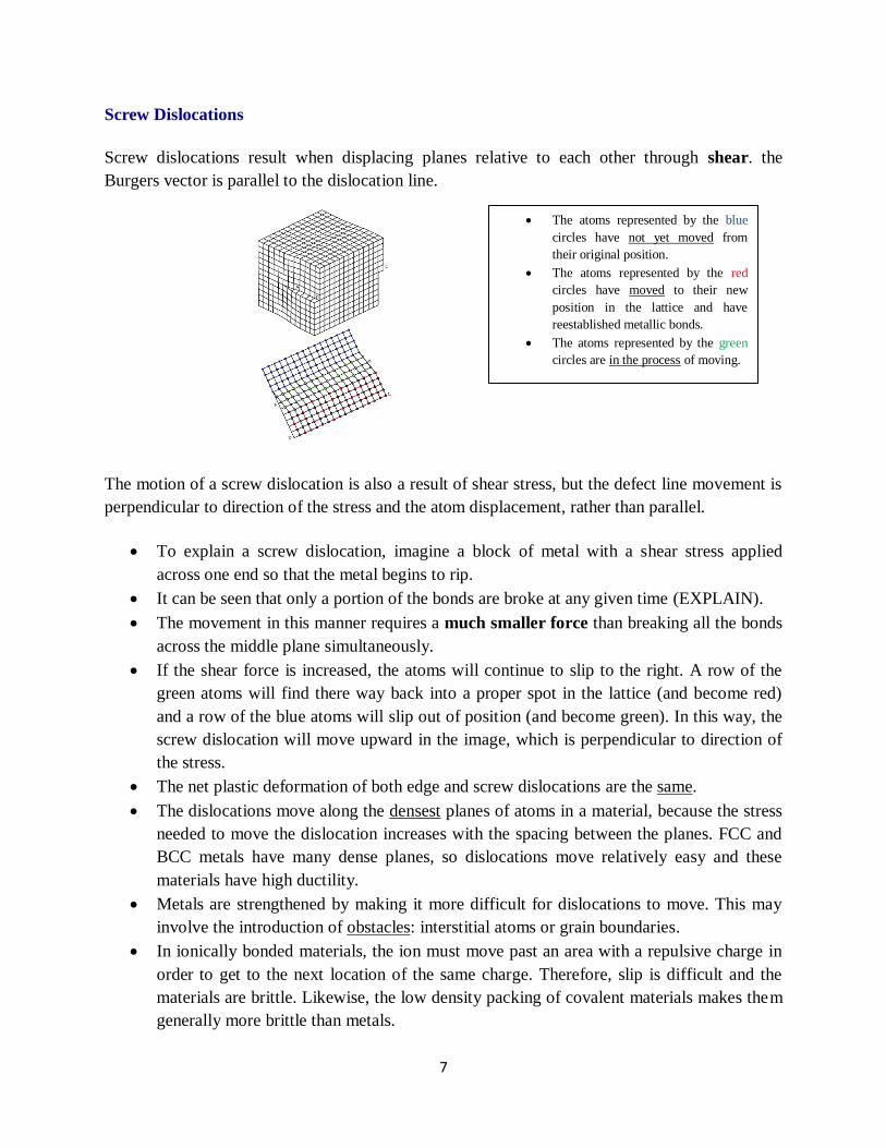
Screw Dislocations
Screw dislocations result when displacing planes relative to each other through shear. the
Burgers vector is parallel to the dislocation line.
The motion of a screw dislocation is also a result of shear stress, but the defect line movement is
perpendicular to direction of the stress and the atom displacement, rather than parallel.
To explain a screw dislocation, imagine a block of metal with a shear stress applied
across one end so that the metal begins to rip.
It can be seen that only a portion of the bonds are broke at any given time (EXPLAIN).
The movement in this manner requires a much smaller force than breaking all the bonds
across the middle plane simultaneously.
If the shear force is increased, the atoms will continue to slip to the right. A row of the
green atoms will find there way back into a proper spot in the lattice (and become red)
and a row of the blue atoms will slip out of position (and become green). In this way, the
screw dislocation will move upward in the image, which is perpendicular to direction of
the stress.
The net plastic deformation of both edge and screw dislocations are the same.
The dislocations move along the densest planes of atoms in a material, because the stress
needed to move the dislocation increases with the spacing between the planes. FCC and
BCC metals have many dense planes, so dislocations move relatively easy and these
materials have high ductility.
Metals are strengthened by making it more difficult for dislocations to move. This may
involve the introduction of obstacles: interstitial atoms or grain boundaries.
In ionically bonded materials, the ion must move past an area with a repulsive charge in
order to get to the next location of the same charge. Therefore, slip is difficult and the
materials are brittle. Likewise, the low density packing of covalent materials makes them
generally more brittle than metals.
The atoms represented by the blue
circles have not yet moved from
their original position.
The atoms represented by the red
circles have moved to their new
position in the lattice and have
reestablished metallic bonds.
The atoms represented by the green
circles are in the process of moving.

8
III) Interfacial Defects (Surface defects):
Come form: between different phases, or between different crystals. It may arise at the boundary
between two grains, or small crystals, within a larger crystal. The rows of atoms in two different
grains may run in slightly different directions, leading to a mismatch across the grain boundary.
The actual external surface of a crystal is also a surface defect because the atoms on the surface
adjust their positions to accommodate for the absence of neighboring atoms outside the surface
1) (External Surfaces) : The environment of an atom at a surface differs from that of an atom in
the bulk, in that the number of neighbors (coordination) decreases. This introduces unbalanced
forces which result in relaxation (the lattice spacing is decreased) or reconstruction (the crystal
structure changes). Surface atoms have unsatisfied atomic bonds, and higher energies than the
bulk atoms ⇒ Surface energy, γ (J/m2)
• Surface areas tend to minimize (e.g. liquid drop)
• Solid surfaces can “reconstruct” to satisfy atomic bonds at surfaces.

9
2) Grain Boundaries : Polycrystalline material comprised of many small crystals or grains. The
grains have different crystallographic orientation. There exist atomic mismatch within the
regions where grains meet. These regions are called grain boundaries. Surfaces and interfaces are
reactive and impurities tend to segregate there. Since energy is associated with interfaces, grains
tend to grow in size at the expense of smaller grains to minimize energy. This is accelerated at
high temperatures. The density of atoms in the region including the grain boundary is smaller
than the bulk value, since void space occurs in the interface.
It is convenient to separate grain boundaries by the extent of the mis-orientation between the
two grains.
•low angle grain boundaries : are those with a misorientation less than about 11 degrees.
• high angle grain boundaries : whose misorientation is greater than about 11 degrees
3. Twin boundaries
10
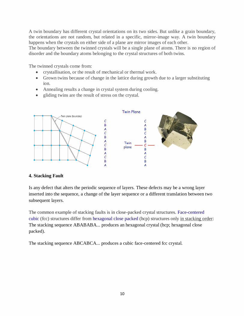
A twin boundary has different crystal orientations on its two sides. But unlike a grain boundary,
the orientations are not random, but related in a specific, mirror-image way. A twin boundary
happens when the crystals on either side of a plane are mirror images of each other.
The boundary between the twinned crystals will be a single plane of atoms. There is no region of
disorder and the boundary atoms belonging to the crystal structures of both twins.
The twinned crystals come from:
crystallisation, or the result of mechanical or thermal work.
Grown twins because of change in the lattice during growth due to a larger substituting
ion.
Annealing results a change in crystal system during cooling.
gliding twins are the result of stress on the crystal.
4. Stacking Fault
Is any defect that alters the periodic sequence of layers. These defects may be a wrong layer
inserted into the sequence, a change of the layer sequence or a different translation between two
subsequent layers.
The common example of stacking faults is in close-packed crystal structures. Face-centered
cubic (fcc) structures differ from hexagonal close packed (hcp) structures only in stacking order:
The stacking sequence ABABABA... produces an hexagonal crystal (hcp; hexagonal close
packed).
The stacking sequence ABCABCA... produces a cubic face-centered fcc crystal.

11
IV)Volume defects
Are two-dimensional such as cracks may arise in crystals during the process of crystal
growth.
While growing, any possible small electrostatic dissimilarity between the stacking layers
may result in crack.
A large vacancy may arise due to missing of clusters of atoms which is a volume defect.
Inclusion of foreign particles or non- crystalline regions of dimensions of at least 10-30Å
also belong to the category of volume defects.