Effect of a micro dielectric barrier discharge plasma actuator on quiescent flow
Upload
independentCategory
view
4download
0
1
Defect Detection Using Quiescent Signal Analysis
Chintan Patel, Abhishek Singh and Jim PlusquellicDepartment of CSEE, University of Maryland, Baltimore County
Paper No: JETT808-02
Contact Author:
Chintan Patel
University of Maryland Baltimore County
ITE 322, CSEE Dept.,
1000 Hilltop Circle,
Baltimore, MD 21250.
Phone: 410-455-3963.
E-mail: [email protected].
Fax: 410-455-3969.

2
Defect Detection Using Quiescent Signal Analysis
Authors:
Chintan Patel, [email protected]
Abhishek Singh, [email protected]
Jim Plusquellic, [email protected]
Address:Department of CSEE, University of Maryland, Baltimore County
1000 Hilltop Circle, Baltimore, MD - 21250.
Abstract
IDDQ or steady state current testing has been extensively used in the industry as a mainstream defect detec-
tion and reliability screen. The background leakage current has increased significantly with the advent of ultra deep
submicron technologies. This increased background leakage noise makes it difficult to differentiate defect-free devices
from those with defects that draw significantly small amount of currents. Therefore it is impossible to use single
threshold IDDQ testing for today’s technologies. Several techniques that improve the resolution of IDDQ testing have
been proposed to replace the single threshold detection scheme. However, even these techniques are suffering from
loss of resolution that is required for detection of subtle defects in the presence of leakage currents in excess of a few
mA. All these techniques use a single IDDQ measurement for detection and thus the scalability of these techniques is
limited. Quiescent Signal Analysis (QSA) is a novel IDDQ defect detection and diagnosis technique that uses IDDQ
measurements at multiple chip supply pads. Implicit in our methodology is a leakage calibration technique that scales
the total leakage current over multiple simultaneous measurements. This helps in decreasing the background leakage
component in individual measurements and thus increases the resolution of this technique to subtle defects. Defect
detection is accomplished by applying linear regression analysis to the multiple supply port measurements and using
outlier analysis to identify defective devices. The effectiveness of this technique is demonstrated in this paper using
simulation experiments on portion of a production power grid. Predicted chip size and leakage values from the Inter-
national Technology Roadmap for semiconductors (ITRS) are used in these experiments. One of the other major con-
cerns expressed in ITRS is that of significant increase in intra-die process variations. The performance of the

3
proposed technique in presence of such variations is evaluated using three different intra-die process variation distri-
bution models.
1.0 Introduction
The advantages of analyzing power grid signals were recognized more than a decade ago with the introduction of
IDDQ testing. Here, an elevation in the steady-state current of a chip beyond a threshold was determined to be a reli-
able indication of the presence of a shorting defect in the circuit under test (CUT). Unfortunately, advances in silicon
technology, in combination with increases in chip size and transistor density, have caused increases in the background
steady-state current of defect-free chips, making it difficult to distinguish the defective chips using a single threshold
technique [1]. Along with the increase in the magnitude of background leakage current, the variability in the current
value from chip-to-chip (inter-die) as well as between different regions of a particular chip (intra-die) has increased
significantly. However, the properties of the power grid continue to remain attractive from a testing perspective, and
alternative multi-threshold IDDQ methods and novel transient techniques are drawing considerable attention.
Several techniques like Current Signature [2], Delta IDDQ [3] and Current Ratios [4] have been proposed by vari-
ous authors to calibrate for these high subthreshold leakages. These techniques rely on a self-relative or differential
analysis, in which the average IDDQ of each device is factored into the pass/fail threshold. However, these calibration
methods are expected to become increasingly less effective over successive technology generations. The ability of
these techniques to differentiate small subtle defect currents from very high and varying background leakage currents
is expected to reduce. This is due to the fact that the different set of thresholds employed by these techniques will
increase with increasing magnitude and variance of IDDQ. Although these techniques may become infeasible to
employ for high performance ASICs with high background leakage currents their application to low power chips with
relatively low leakage currents will continue.
An alternate calibration strategy that may have better scaling properties is to distribute the total leakage current
across a set of measurements. This is accomplished by introducing probing hardware either on chip or off chip that
allows access to individual power supply ports. The method proposed in this work called Quiescent Signal Analysis
(QSA), is designed to exploit this type of leakage calibration as a means to increase the defect detection capabilities
and resolution. An important application of such a technique, based on the current distribution profile is that it pro-

4
vides information about the defect’s location in the layout [9]-[12].
A linear regression analysis procedure is proposed for QSA that calibrates for high background leakage currents.
This procedure is derived from our previous work on Transient Signal Analysis [13]. In TSA, multiple power supply
transient signals are analyzed simultaneously as a means of both detecting the regional signal variations introduced by
defects and diminishing the signal variations introduced by process variation effects. In QSA, this procedure performs
a similar function of distinguishing globally distributed leakage current from the regional defect current.
In this work, an extensive set of spice simulations are used to demonstrate the defect detection capabilities of QSA
in presence of significant background leakage noise and three different intra-device process variation models. The
analysis is performed on a portion of a Production Power Grid (PPG) referred to as Q9. The simulation models were
derived using projected values for chip size, number of power supply ports and leakage currents obtained from the
International Technology Roadmap for Semiconductors (ITRS) [14]. As it is infeasible to run spice simulations on the
whole chip, the simulation models were derived by scaling the whole chip values by the ratio of size of the chip to
that of the Q9. The Q9 has dimensions of 30000 x 30000 units and consists of 16 VDD C4 pads from which individual
IDDQ measurements are made. The defect-free devices were modeled using leakage values in the range of 1mA to
150mA for the whole chip. These values were determined from the ITRS and cover high and medium performance,
medium power and low power devices. Three different intra-device process variation distributions were used in com-
bination with the above mentioned base leakage values to generate 48 defect free models. Two of the local variation
models were symmetric or regular in nature while the third model was random. The base leakage values were varied
by +/- 2.5% and +/- 5% in each of these models. 1800 defect models were generated using defect values in the range
of 10µA to 100µA in combination with the above mentioned defect-free models to determine the detection sensitivity.
The rest of this paper is organized as follows. Section 2.0 outlines some related work. Section 3.0 describes the
regression analysis procedure for QSA. Section 4.0 describes the production power grid used for the simulations. Sec-
tion 5.0 describes the experimental setup. Section 6.0 presents the experimental results and discusses these results and
Section 7.0 give a summary and conclusions.
2.0 Related Work
Single-threshold IDDQ technique relied on the fact that the steady state current distribution of defect-free devices

5
is distinct from that of the defective ones. A device that draws current that exceeds the defect-free current distribution
by a fixed threshold is deemed as defective. With the advent of deep sub-micron technologies, the overlap in these
distributions makes it difficult to set an absolute pass/fail threshold. The increase in sub-threshold leakage currents in
newer technologies can result in defect-free leakage currents that are significantly higher than the defect current.
Thus, calibration methods are required to reduce the adverse effects of high leakage currents and increase the resolu-
tion to defect currents. Several techniques based on a self-relative or differential analysis are proposed as a solution to
this problem. A current signature method is proposed by Gattiker et. al. [2], that looks for discontinuities in the curve
obtained by sorting IDDQ measurements in ascending order. Delta IDDQ is a differential IDDQ method proposed by
Thibeault [3] in which differences between successive IDDQ measurements are compared to a threshold. Maxwell et.
al. [4], proposed a current ratio method where chip specific thresholds are derived by using vectors that produce the
minimum and maximum IDDQ values. A regression line was drawn through a scatter plot representing the ratio of
minimum to maximum IDDQ of a set of known defect-free chip. The threshold is set by allowing a guard band around
this regression line to account for process variations. A clustering technique that groups good devices separately from
bad devices is proposed by Jandhyala et. al. [5]. Dies in a particular cluster are inherently related to each other. As all
readings from all vectors are used for clustering this technique calibrates for process variations. Daasch et. al. [6]
describe a method that predicts device IDDQ using the spatial proximity correlations among devices on a wafer.
Variyam [7] proposes a linear prediction based technique in which each IDDQ value among a set of values for a given
chip is predicted from the remaining IDDQ values in the set. Singh et. al [8] showed that IDDQ readings of the neigh-
boring die on a wafer can be used for variance reduction.
Many of these process-tolerant IDDQ methods use relative pass/fail thresholds instead of absolute thresholds. Also
the other major similarity in all of the above techniques is that they use a single IDDQ measurement per vector per die.
As variance in the IDDQ values increase it tends to increase the threshold bands in most of these techniques, thus
decreasing their defect resolution. Our method, Quiescent Signal Analysis or QSA, differs from these methods, in
which correlation is carried out between individual supply IDDQs within each state vector. A regression analysis pro-
cedure in combination with outlier analysis is used to differentiate defect-free and defective devices. Therefore, the
cross-correlation performed in QSA additionally calibrates for vector-to-vector variations. This is likely to further

6
improve the process tolerance of the method. Also this method can be used in combination with all of the above men-
tioned vector-to-vector analysis techniques to further improve defect resolution.
Another advantage of a method that uses multiple supply port measurements is the natural scalability that this
approach incorporates. The scalability features of the method should make it possible for it to remain effective at
detecting defects as chips get larger and incorporate larger numbers of more densely packed transistors. QSA is
designed to exploit design trends that add additional supply ports (pads that interface to the external supply) as chip
sizes and current requirements increase. However, it should be noted that this benefit of increased resolution comes
with the cost of increase in the test time as multiple measurements need to be performed per vector.
Perhaps a greater benefit of using multiple power supply signals is that they offer information beyond defect
detection. In our previous work, we have demonstrated the ability of QSA for application to defect diagnosis [9]-[12].
The procedure predicts the (x,y) coordinates at which a defect draws current from the power grid in the layout. To our
knowledge, no other method that is based on the analysis of a chip’s electrical signals is able to provide this type of
information. Such information is extremely useful in failure analysis procedures, which are designed to determine the
root cause of chip failures.
3.0 QSA Detection Procedure
QSA analyzes a set of IDDQ measurements, each obtained from individual supply pads from the Chip-Under-Test
(CUT). The resistive nature of the power grid causes the current drawn by the defect to be non-uniformly distributed
to each of the supply pads. In particular, the defect draws the largest fraction of its current from supply pads topolog-
ically “nearby”. The same is true of the leakage currents. However, only the leakage currents in the vicinity of the
defect contribute to the measured current in these pads. The smaller background leakage component improves the
accuracy of the defect current measurement.
The fraction of the defect current provided by each of the pads in the region of the defect is proportional to the
equivalent resistance between the defect site and each of the pads. Consider the resistance model of a simple power
supply grid as shown in Figure 1.
Figure 1. Equivalent resistance network with defect inside the circuit.
Here, Req0 through Req3 represent the equivalent resistances between each of the supply pads and the defect site

7
shown in the center of the figure. The following set of equations describe the relationship between the power supply
branch currents, I0 through I3, Rp the probe card resistance and Vdef, the voltage at the defect site.
Consider the example shown in Figure 1. As the defect is topologically closer to VDD3, it will have the lowest
equivalent resistance to that pad and thus source the highest amount of current from that pad. Therefore, a defect
causes regional variations where the current drawn from each pad is dependent on the equivalent resistance.
The defective device’s IDDQ consists of two components, the current drawn by the defect, and the process and
technology-related leakage current, e.g. subthreshold leakage current. If the transistor density in the layout is regular,
then the leakage current will be distributed evenly among all the supply ports. Each supply port in this case draws the
same amount of leakage current as the other ports. A defect, in such a scenario, will cause more current to be sourced
from a topologically closer pad and can be detected. However if the transistor density in the layout varies across the
design, shown for example in Figure 2, the leakage current sourced by each supply pad will vary. This is due to the
fact that the leakage current will be distributed by the power grid proportionally, as a function of resistance. This
localized variation of the leakage currents will adversely affect a regional information based defect detection scheme.
Figure 2. Unequal transistor densities in the layout.
The key observation concerning leakage current is that it is effected most significantly by the global variations
introduced by changes in process and technology-related parameters. In other words, the current variations introduced
by variations in these parameters will affect all transistors and junctions in a device in a similar manner. We are not
claiming that intra-device variations do not exist, but rather, they are smaller in magnitude. The global nature of pro-
cess variations scale the leakage currents to all supply ports, making it possible to track it using regression analysis.
Linear regression is used to track these global background leakage currents and provides a means of distinguish-
ing them from the regional defect currents. The procedure is based on the analysis of scatter plots obtained by plotting
the IDDQ values at two supply ports. For example, Figure 3 represents a power grid with 16 VDD supply ports. A set of
defect-free spice simulations are run on the circuit where the leakage under each simulation is varied randomly across
the grid.
Ii Reqi Rp+( )× VDD V–def
= for i = 0,1,2,3 (1)
8
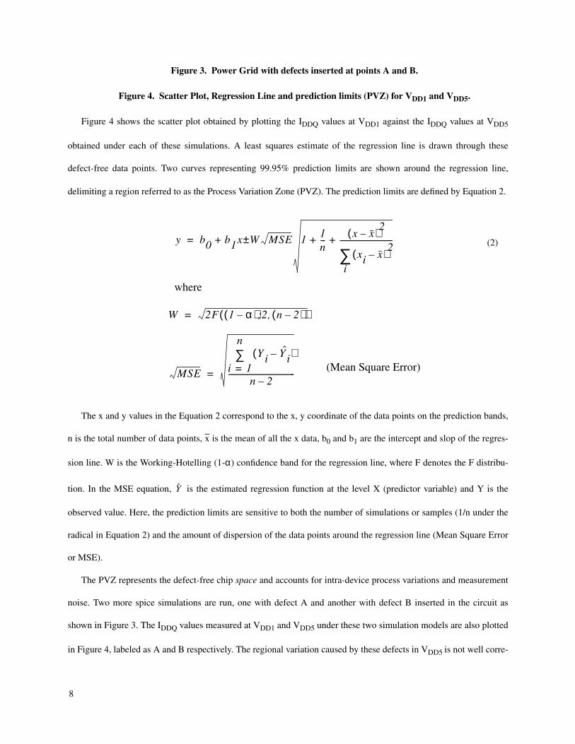
Figure 3. Power Grid with defects inserted at points A and B.
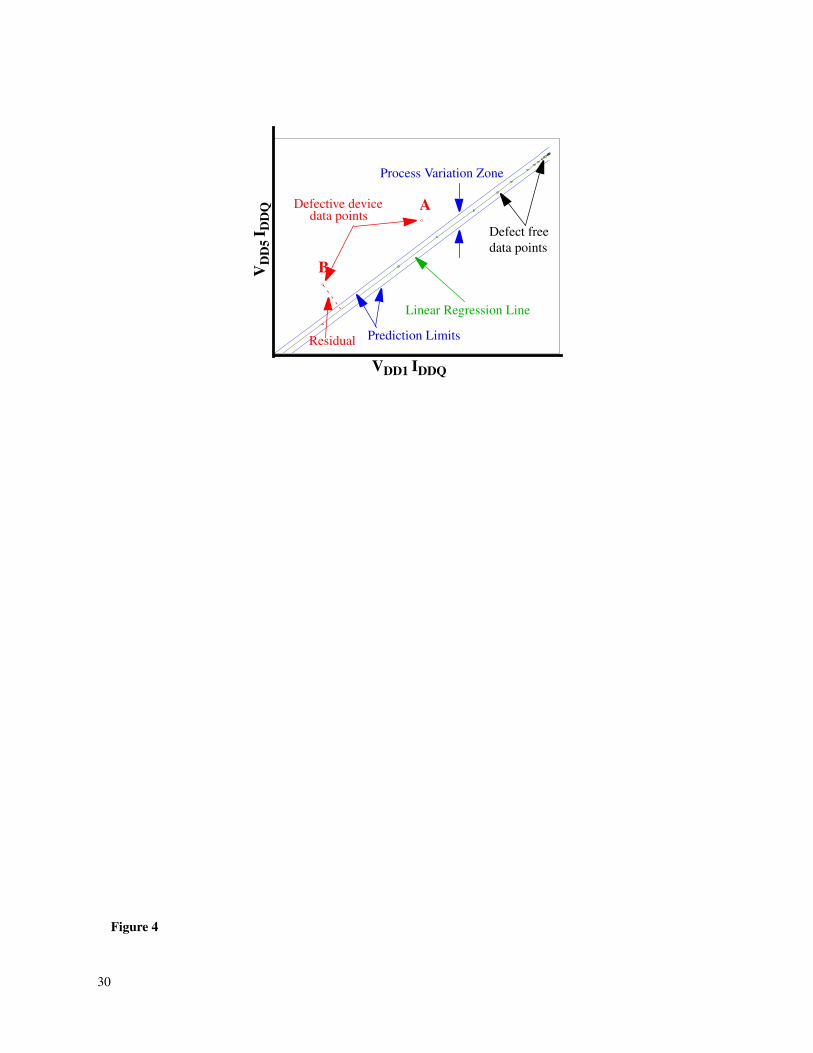
Figure 4. Scatter Plot, Regression Line and prediction limits (PVZ) for VDD1 and VDD5.
Figure 4 shows the scatter plot obtained by plotting the IDDQ values at VDD1 against the IDDQ values at VDD5
obtained under each of these simulations. A least squares estimate of the regression line is drawn through these
defect-free data points. Two curves representing 99.95% prediction limits are shown around the regression line,
delimiting a region referred to as the Process Variation Zone (PVZ). The prediction limits are defined by Equation 2.
The x and y values in the Equation 2 correspond to the x, y coordinate of the data points on the prediction bands,
n is the total number of data points, x is the mean of all the x data, b0 and b1 are the intercept and slop of the regres-
sion line. W is the Working-Hotelling (1-α) confidence band for the regression line, where F denotes the F distribu-
tion. In the MSE equation, is the estimated regression function at the level X (predictor variable) and Y is the
observed value. Here, the prediction limits are sensitive to both the number of simulations or samples (1/n under the
radical in Equation 2) and the amount of dispersion of the data points around the regression line (Mean Square Error
or MSE).
The PVZ represents the defect-free chip space and accounts for intra-device process variations and measurement
noise. Two more spice simulations are run, one with defect A and another with defect B inserted in the circuit as
shown in Figure 3. The IDDQ values measured at VDD1 and VDD5 under these two simulation models are also plotted
in Figure 4, labeled as A and B respectively. The regional variation caused by these defects in VDD5 is not well corre-
y b0 b1x W± MSE 11n---
x x–( )2
xi x–( )2
i∑----------------------------+ ++=
W 2F 1 α–( ) 2 n 2–( ),;( )=
where
MSE
Yi Yiˆ–( )
i 1=
n∑
n 2–-----------------------------------=
(2)
(Mean Square Error)
Y

9
lated with the variation measured at VDD1 on the same chip. The large IDDQ at VDD5 in combination with the small
IDDQ at VDD1 generates data points outside the PVZ. For this pairing of VDDs, the position of the data points outside
the PVZ suggests that the last two circuit models are defective.
The standard statistical method of analyzing variance in scatter plots is through residuals. A residual is defined to
be the shortest distance from a data point to the regression line, as shown in Figure 4. Residual Analysis, used in com-
bination with the 99.95% prediction limits, make it straightforward to decide the pass/fail status of a chip. If more
than one scatter plots are analyzed, a test chip fails if it produces at least one data point outside the corresponding
PVZs.
One metric to evaluate the effectiveness of the technique would be to count the number of pairings for which the
defective device data points fall outside the PVZ. However, in addition to this metric, it is also meaningful to examine
the magnitudes of the residuals. In order to make this value meaningful for comparisons with other values, the magni-
tude of the residuals are normalized or standardized using Equation 2.
Here, MSE is the variance of the defect-free simulation residuals. For the experiments in this paper, the prediction
bands are used as the pass/fail threshold for identifying the defective devices and the ZRES values are used to evalu-
ate the confidence of the prediction. In other words, a device fails if at least one data point falls outside of a predeter-
mined prediction band for any VDD pairing. Moreover, the confidence that a test device is defective is higher for
larger values of ZRES.
4.0 Production Power Grid
Figure 5 shows the 80,000 by 80,000 unit layout of the PPG. The PPG interfaces to a set of external power sup-
plies through an area array of VDD and GND C4 pads. A C4 pad is a solder bump for an area array I/O scheme. The
PPG has 64 VDD C4s and 210 GND C4s (not shown in Figure 5). The 64 VDD C4s divide the PPG into 64 different
regions called Quads. Due to space and time constraints, it was not possible to run spice simulations on the entire
PPG. Rather, a portion of the PPG consisting of 9 quads was simulated using spice. This portion consists of the lower
left 9 Quads as shown in Figure 5, and is subsequently referred to as the Q9. The Q9 occupies a 30,000 by 30,000 unit
ZRESresidual
MSE-------------------= (3)

10
area and has 16 VDD C4’s.
Figure 5. Layout of the PPG.
Figure 6. Detail of the “Quad”: Portion of the PPG.
Figure 6(a) expands on the lower left corner of the PPG by showing a more detailed diagram of the 10,000 by
10,000 unit region called the Quad. This is again expanded in Figure 6(b). At this level, it can be seen that the grid is
constructed over 4 layers of metal with metal 1 and 3 running vertically and metal 2 and 4 running horizontally. The
C4s are connected to wide runners of vertical metal 5, indicated as m5 in Figure 6(a), that are in turn connected to the
m1-m4 grid. In each layer of metal, the VDD and GND rails alternate. In the vertical direction, each metal 1 rail is
separated by a distance of 432 units. The alternating vertical VDD and GND rails are connected together using alter-
nating horizontal metal runners. Stacked contacts are placed at the appropriate crossings of the horizontal and vertical
rails.
The R model of the PPG was obtained from an extraction script using parameters characterizing TSMC’s 0.25µm
process. A well characterized probe card model described in [15] was used to model the tester power supply and
probe card contact resistance to the chip. The combined resistance network contains approximately 27,000 resistors
per quad.
5.0 Simulation Models
The simulation models were derived according to the current technology node, the expected chip size and nominal
IDDQ for different categories of chips as described in the ITRS. The maximum IDDQ for high performance ASICs is
predicted to be anywhere from 70mA to 150mA. IDDQ for low power, low speed chips will be significantly lower than
these values and can be anywhere from 1mA to a few tens of mA. The area of the chip, once is production, is pre-
dicted to stay relatively constant around 140 mm2. The total number of VDD/GND pads would be around 1700 for
high performance ASICs out of which we expect 1/3rd will be VDDs (400 - 500 pads). As mentioned earlier, due to
memory and time constraints it is infeasible to run simulations using the power grid for the whole chip. Therefore a
portion of the chip namely the Q9 is used for running simulations to validate the proposed technique. The IDDQ and
chip area values shown above are scaled to derive the background leakage values for the Q9. The area of Q9, if fabri-

11
cated in the 0.13µm technology node, would be 4.85 mm2. Therefore, if the IDDQ for the whole chip is about 150 mA
the IDDQ for the Q9 will be around 5.2 mA. To ensure that the model is not overly optimistic the number of VDD pads
can be compared. There are 16 VDD pads in the Q9 which would translate to about 340 VDD pads in the whole chip.
This number is lower than the actual number of VDD pads predicted for the whole chip indicating that the model is
not overly optimistic, as it uses less measurement points than available.
As the background leakage current has a wide range depending on the type of chip being tested a range of 1mA to
150mA was used to model the leakage current. 19 values were selected in this range as the base leakage values for
defect-free chips and the corresponding leakage values for the Q9 were derived. 8 of these values were in the range of
70mA to 150mA to model high performance ASICs. The other 11 were from 1mA to 70mA that model medium and
low power chips. The values in each of these subsets model chip-to-chip or inter-device process variations in the base
leakage. The leakage current is modeled by placing about 31,500 current sources on the metal1 rails in the Q9. The
metal1 rails in the layout represent the transistor density in a particular region. Regions with higher transistor densi-
ties have more metal1 rails than regions with lower transistor densities. Placing the leakage sources regularly along
the metal1 rails emulates the effect of having irregular transistor densities in the layout.
With decreasing device dimensions, one of the other major problems facing most parametric testing techniques is
that of intra-device or region-to-region process variations. Although these local variation effects are significantly
lower than the global inter-device leakage variations they cannot be ignored for current and future technology nodes.
These variations can be caused during any of the several complex processing steps and are thus hard to model. They
could either be completely random over the whole chip or could vary in different regions of the chip in a regular fash-
ion. For deriving our simulation models, we consider three different intra-device process variation distributions, one
random and two regular in nature.
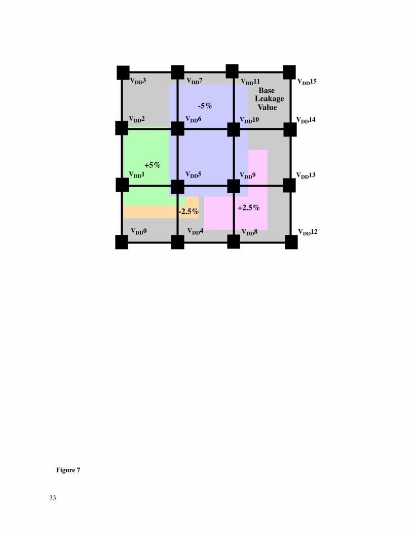
The random distribution is modeled by first creating 4 random boxes with known minimum dimensions over the
Q9 as illustrated in Figure 7. The value of the leakage sources that fall within each of these 4 regions were varied by
+/-2.5% and +/-5%. As the Q9 only models a portion of the chip the total variation in leakage current values and dis-
tribution will be higher when translated to the whole chip. This model is referred to as Random-Boxes.
Figure 7. Random-Boxes (random distribution) model for local variations.

12
The first regular distribution model is called Edge-to-Edge and is illustrated in Figure 8. Here the base leakage
sources are varied from +5% to -5% from one edge to the other. 20 rectangular vertical slices are generated where the
variation in each slice is 0.5%. Although the overall leakage current is not affected significantly, this type of variation
changes the local leakage distribution in different regions of the Q9.
Figure 8. Edge-to-Edge (regular distribution) model for local variations.
The last model is also a regular distribution as shown in Figure 9 and is referred to as Center-Out. Here 20 squares
are generated and the base leakage sources are varied by -5% from the center to +5% at the outermost square, with a
0.5% variation per square. This model will not only change the local leakage distribution but also affect the overall
leakage current as the size of the squares gradually increase as we move away from the center.
Figure 9. Center-Out (regular distribution) model for local variations.
Using the 19 base leakage values mentioned above and the 3 local variation distributions a total of 76 defect free
simulation models were derived. 19 models incorporated no local variations and were just the base leakage values.
The others were combinations of each of these 19 models with (1) Random-Boxes with +/-2.5% and +/-5% variation
regions, (2) Edge-to-Edge variation of +/-5% and (3) Center-Out variation of +/-5%. A defect is modeled by inserting
one extra current source among the 31,500 leakage sources. Defects were placed in the quad located in the center of
Q9 as shown in Figure 10 and referred to as the Center Quad. 100 defect locations were selected in the Center Quad
such that they are regularly distributed in a two-dimensional mesh like structure as shown in the figure. Different
defect current values in combination with a leakage current model from above and the 100 defect locations were used
to generate 1800 defective device simulation models.
Figure 10. Center Quad and defect locations.
6.0 Results and Discussion
Defect simulations were run using six different defect current and base current combinations. The base leakage
boundary values for high performance devices were used for the defect simulations and as described earlier, they
were scaled by the dimensions of Q9. Each of these combinations, shown in Table 1, were used in conjunction with

13
the 100 defect locations and 3 different local variation models to derive the 1800 defective device models.
The defect draws the maximum amount of current from pads topologically closer to the defect site. Thus most of
the defect current sourced by a defect in any quad, is supplied by the four VDD pads that constitute the defective quad.
In other words, the defect causes minimal change in the current sourced by pads outside the defective quad as com-
pared to the defective quad pads. This helps in reducing the number of VDD pairings analyzed for defect detection.
The probability of detection is higher in each of the scatter plots that include one pad from the defective quad in com-
bination with a pad from a neighboring quad. For example, if the defect is located in the Center Quad in Figure 10,
most of the current drawn by the defect is supplied by VDD pads VDD5, VDD6, VDD9 and VDD10. The VDD pairings
with the highest detection probability in this case will be, VDD1-VDD5, VDD4-VDD5, VDD5-VDD9, VDD5-VDD6,
VDD2-VDD6, VDD6-VDD7, VDD6-VDD10, VDD10-VDD11, VDD10-VDD14, VDD10-VDD9, VDD9-VDD13 and
VDD9-VDD8. Thus for any defect in the Center Quad we need to analyze the scatter plots obtained using the above 12
VDD pairings. A similar procedure can be used to construct the scatter plot combinations for defects that occur in
other quads.
This reduced set of scatter plots can be analyzed only if the defective quad can be identified. In most cases, it is
simple to identify the defective quad by sorting the IDDQs drawn from each pad in descending order. If the first three
Defect NumberChip BaseLeakageCurrent
Scaled Q9Base Leakage
Current
DefectCurrent
1 150mA 5.192mA 100µA
2 150mA 5.192mA 50µA
3 150mA 5.192mA 25µA
4 70mA 2.422mA 50µA
5 70mA 2.422mA 25µA
6 70mA 2.422mA 10µA
Table 1: Defect and base leakage combinations used for defect simulations.

14
pads are non-colinear and constitute a quad then that quad is the defective quad. However, if the defect is very close to
the boundary of two quads this condition might not hold. Consider the defect marked A in Figure 10. This defect will
draw maximum current from VDD10. The second and third highest in the list can be VDD9, VDD11, VDD6 or VDD14,
depending on the resistance profile of the grid in that region. In such cases, either all possible scatter plots for each of
these quads can to be considered or a technique similar to the one proposed in our previous work on defect diagnosis
using QSA can be used to identify the defective quad [12]. The second solution requires a small DFT structure to be
inserted under each VDD C4 (see [12] for details).
6.1 Edge-to-Edge Local Variation Model
A total of 600 defect simulation models incorporated this type of local variation. The defect free scatter plots were
generated using 38 defect free models namely, 19 base defect-free models and 19 base defect-free models combined
with Edge-to-Edge variation of +/-5%. The data analysis for these set of simulations is presented in Table 2. As
Defect # 1 Defect # 2 Defect # 3 Defect # 4 Defect # 5 Defect # 6
Total number of defects 100 100 100 100 100 100
Defects detected 100 100 100 100 100 100
Average number ofdetections over all scatterplots
9.03 7.18 6.09 6.91 5.88 5.01
# SP pairing Detections per scatter plot (SP) pairing
1 SP VDD1-VDD5 31 6 0 12 0 0
2 SP VDD4-VDD5 100 100 100 100 100 100
3 SP VDD5-VDD9 40 15 5 14 1 0
4 SP VDD5-VDD6 98 95 86 95 87 63
5 SP VDD2-VDD6 29 5 0 12 0 0
6 SP VDD6-VDD7 100 100 96 100 99 66
Table 2: Edge-to-Edge Local Variation Detection Data

15
shown in the first two rows of the table all the 600 defects were detected in this case. Also shown is the average num-
ber of detections for all the defects over all the scatter plots. A higher number suggests that each defect was detected
multiple number of times in different scatter plots. The efficiency of each scatter plot pairing can be determined by
looking at the total number of detection per scatter plot also shown in the table. As seen from the trends in the first
and last three columns the detection sensitivity is dependent on the magnitude of the defect current. However, in the
case of 150mA base leakage current the change in defect current from 100µA to 25µA, a factor of 4, causes only a
change from 9.06 to 6.09 average detections per defect.
The higher probability of detections in this case would be for scatter-plots between pads that are well correlated in
presence of this type of intra-device process variations. Closely studying Figure 8 reveals that all scatter plots
between VDD pads that are located vertically adjacent to each other should provide the best results. This is confirmed
by looking at the number of detections per scatter plot, where all such scatter plots consistently have higher number of
detections than the ones that analyze horizontally adjacent VDD pads.
Figure 11. Edge-to-Edge model: Maximum Zdiff values and scatter plot distribution for defect # 3.
Figure 11(a) shows the detection sensitivity for all the 100 defect locations over the 12 scatter plot pairings for
defect #3. This defect model has the minimum defect current in the presence of 150mA of base leakage current. The
x and the y axis give the location of the defect in the center quad and the z dimension reports the maximum difference,
7 SP VDD6-VDD10 38 15 3 10 0 0
8 SP VDD8-VDD9 100 100 100 100 100 99
9 SP VDD9-VDD13 84 45 14 27 4 0
10 SP VDD9-VDD10 100 97 93 97 93 75
11 SP VDD10-VDD14 83 40 12 24 4 0
12 SP VDD10-VDD11 100 100 100 100 100 98
Defect # 1 Defect # 2 Defect # 3 Defect # 4 Defect # 5 Defect # 6
Table 2: Edge-to-Edge Local Variation Detection Data

16
Zdiff, between the standardized residuals (ZRES) of a defective device data point and the prediction band. The maxi-
mum Zdiff value gives the measure of confidence with which a device can be deemed as defective. In cases where the
device data point falls outside the prediction bands of more than one scatter plot the probability of false detection is
reduced. However, if the device data point is an outlier in only one or very few scatter plots then a safety threshold can
be used for the minimum value of Zdiff required in at least one scatter plot to deem the device defective. If the maxi-
mum Zdiff value reported here is greater than the threshold the device can be identified as defective. As described ear-
lier in Section 3, the standardized residuals are computed as the ratio of the defective device residual and the square
root of the MSE. The MSE of a particular scatter plot is determined by variance of the defect free residuals. Thus
scatter plots with highly correlated defect free device data points will have lower MSE values and thus higher detec-
tion sensitivity. For the Edge-to-Edge model, the correlation coefficients of SP # 2, 8 and 12 are very high, with 2
being the highest. Thus the maximum Zdiff values are obtained in SP # 2 in most cases as shown in Figure 11(b). Sim-
ilar plots are shown in Figure 12 for the other extreme defect # 6, that has the least defect current with 70mA of base
leakage. The distribution is similar in both cases however, the maximum Zdiff values are lower due to lower defect
current.
Figure 12. Edge-to-Edge model: Maximum Zdiff values and scatter plot distribution for defect #6.
6.2 Center-Out Local Variation Model
A total of 600 defect simulation models incorporated this type of local variation model. The defect free scatter
plots were generated using 38 defect free models namely, 19 base defect-free models and 19 base defect-free models
combined with Center-Out variations of +/-5%. The data analysis for these set of simulations is presented in Table 3.
Defect # 1 Defect # 2 Defect # 3 Defect # 4 Defect # 5 Defect # 6
Total number of defects 100 100 100 100 100 100
Defects detected 100 100 100 100 100 100
Average number ofdetections over all scatterplots
7.21 4.75 3.3 5.41 3.87 3.3
Table 3: Center-Out Local Variation Detection Data

17
As shown in the first two rows of the table all the 600 defects were detected in this case. Also shown is the average
number of detections for all the defects over all the scatter plots. Compared to the previous model, the affect on detec-
tion sensitivity for this model is higher with decreasing defect currents. Also the absolute values suggest that devices
with this type of variations will be harder to screen than former regular type of variation. Close inspection of Figure 9
would suggest that in this case scatter plots between VDD pads that fall inside the same local variation band should
provide better results. In our case, that translates to scatter plots between the four VDD pads that surround the Center
Quad and this trend in also reflected in the table. For the Center-out model, out of the four possible best case scatter
plots, the correlation coefficients of SP # 3 are the highest. The maximum Zdiff values are obtained in SP # 3 for all
the defect locations. Figure 13(a) and (b) plot defect locations on the x and the y axis and maximum Zdiff values along
# SP pairing Detections per scatter plot (SP) pairing
1 SP VDD1-VDD5 40 11 0 17 1 0
2 SP VDD4-VDD5 41 11 0 20 2 0
3 SP VDD5-VDD9 100 100 100 100 100 100
4 SP VDD5-VDD6 97 95 78 96 91 78
5 SP VDD2-VDD6 37 9 0 17 1 0
6 SP VDD6-VDD7 51 17 0 26 4 0
7 SP VDD6-VDD10 100 98 88 98 96 88
8 SP VDD8-VDD9 41 11 0 20 2 0
9 SP VDD9-VDD13 37 9 0 17 1 0
10 SP VDD9-VDD10 98 94 64 95 87 64
11 SP VDD10-VDD14 33 8 0 14 0 0
12 SP VDD10-VDD11 46 12 0 20 2 0
Defect # 1 Defect # 2 Defect # 3 Defect # 4 Defect # 5 Defect # 6
Table 3: Center-Out Local Variation Detection Data

18
the z axis for defect # 3 and defect # 6, respectively. The maximum Zdiff values for defects that are physically closer
to either of the two pads, considered in SP # 3, are higher than those for defects farther away from these pads.
Figure 13. Center-out model: Maximum Zdiff values for defect #3 (a) and defect #6(b).
6.3 Random-Boxes Local Variation Model
Again, a total of 600 defect simulation models incorporated this type of local variation model. The defect free
scatter plots were generated using 38 defect free models namely, 19 base defect-free models and 19 base defect-free
models combined with Random-Boxes type variations of +/-2.5% and +/-5%. The data analysis for these set of simu-
lations is presented in Table 4. As shown in the first two rows of the table all the defects except some in defect #6
Defect # 1 Defect # 2 Defect # 3 Defect # 4 Defect # 5 Defect # 6
Total number of defects 100 100 100 100 100 100
Defects detected 100 100 100 100 100 81
Average number ofdetections over all scatterplots
9.78 6.99 3.58 8.44 5.26 1.41
# SP pairing Detections per scatter plot (SP) pairing
1 SP VDD1-VDD5 63 26 4 93 52 12
2 SP VDD4-VDD5 86 54 18 92 64 16
3 SP VDD5-VDD9 56 33 12 43 29 11
4 SP VDD5-VDD6 54 28 7 41 27 10
5 SP VDD2-VDD6 94 54 20 100 93 40
6 SP VDD6-VDD7 97 73 30 66 24 0
7 SP VDD6-VDD10 69 51 28 44 22 5
8 SP VDD8-VDD9 99 87 58 86 54 11
9 SP VDD9-VDD13 97 60 24 58 23 1
Table 4: Random-Boxes Local Variation Detection Data

19
were detected in this case. Also it should be noted that 2 defect-free devices fall outside the prediction bands by a very
small margin, when 99.95% confidence limits are used. Chips that incorporate these type of intra-device process vari-
ations are the hardest to screen as the change in leakage distribution over different regions of the chip is random in
nature. More significant variations of random nature can reduce the defect detection sensitivity of this technique. Our
extensive literature study has shown that no data exists on the magnitude or distribution of this type of intra-device
process variations. However, this model was incorporated as it is expected to be present in a real processing environ-
ment. +/-2.5% and +/-%5 variations in the base leakage value might be too high or too low depending on the maturity
and the control of the process. Also we have ensured in the model that the boxes affected by the variations are small
enough to affect the leakage characteristics of the Quad and the Q9. If these type of variations are present over larger
regions, such that they encompass regions bigger than that bounded by the 4 surrounding VDD pads, their adverse
effect on the detection sensitivity will be reduced. If these variations are completely random over very small regions
or even at a single transistor level, we expect that they might be averaged out thus again aiding the detection sensitiv-
ity of our technique. For the Random-Boxes model, defects at all locations for defect # 3 were detected. The maxi-
mum Zdiff plot for this defect model is shown in Figure 14(a) and the scatter plots where these Zdiff values occur are
identified in Figure 14(b).
Figure 14. Random-Boxes: Maximum Zdiff values and scatter plot distribution for defect #3.
As this model is random in nature the correlation coefficients of many scatter plots are comparable and so the
maximum Zdiff values are spread over all these scatter plots. In majority of cases, scatter plots that use VDD pads in
vicinity of the defect location are better at detecting the defect. Also it should be noted that the variance in the defect
free data points is the highest for this model and therefore the maximum Zdiff are significantly lower than the other
10 SP VDD9-VDD10 64 43 18 44 21 3
11 SP VDD10-VDD14 100 100 83 100 78 27
12 SP VDD10-VDD11 99 90 56 77 39 5
Defect # 1 Defect # 2 Defect # 3 Defect # 4 Defect # 5 Defect # 6
Table 4: Random-Boxes Local Variation Detection Data

20
two models. For defect # 6, some defects were missed and the locations of the defects that were not detected for this
defect combination are shown in Figure 15.
Figure 15. Plot of defects missed in model # 6 with Random-Boxes variation.
As shown in the figure, defects farther away from VDD pads are harder to detect as the regional variations in the
current are minimal for those defects. Figure 16(a) shows maximum Zdiff values and Figure 16(b) the scatter plot pair-
ings with these maximum values for the next higher defect (defect # 5) current in presence of 70mA of base leakage
current. The size and location of the random variation boxes are different between the 150mA and 70mA models and
therefore the scatter plot distributions are different for defects in these two models.
Figure 16. Random-Boxes: Maximum Zdiff values and scatter plot distribution for defect #5.
6.4 Random-Boxes Local Variation Model II
The second random-boxes simulation model is presented to show the effect of increasing intra-device process
variation and analysis of defects in various Quads. Rather than using 100 regularly placed defects in the Center Quad,
8 defect locations were selected per Quad of the Q9 for a total of 72 defects. The defect locations in each Quad were
picked randomly and the distribution is shown in Figure 17.
Figure 17. Defect locations for Random-Boxes Model II.
Scaled Q9 base leakages from 500µA to 10mA were used to model the defect free devices. Intra-device process
variations were modeled using four random boxes with +/-5% and +/-10% variation in the base leakage values. The
defect and leakage current combinations used for each of the 8 defects per Quad are given in Table 5.
Defect NumberChip Base
Leakage CurrentScaled Q9 Base
Leakage CurrentDefect
Current
1 288mA 10mA 1mA
2 14.45mA 500µA 1mA
3 288mA 10mA 500µA
Table 5: Defect and leakage current combinations used for Random-Boxes Model II.

21
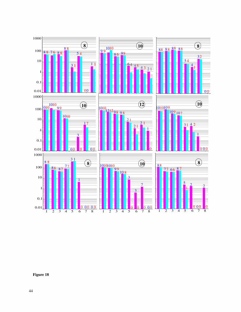
A reduced set of scatter plots were used for the data analysis of each Quad as explained earlier in this Section. The
histogram in Figure 18 summarizes our detection results for all the 72 defects. Each of the histograms in the figure
represents the result in each of the nine Quads. The values on the x-axis are the defect and leakage current combina-
tions given in Table 5. The y-axis has a logarithmic scale and gives the Zdiff of the defective device data point from the
prediction band. The maximum difference from all prediction results is shown as it represents the defect detection
sensitivity of this technique. The values are plotted on a logarithmic scale as a means of improving the visualization
of the wide range of values obtained. The bars on the left in each histogram reports the results when 3σ prediction
limits were used whereas the bar on the right is for 4σ prediction limits. The circled number in the upper right corner
of each graph gives the number of scatter plots considered for the defects in that particular quad. The number on the
top of each defective device bar represents the number of scatter plots in which the defect was detected.
Figure 18. Detection sensitivity and number of detections using 3σ and 4σ prediction bands for all 72defects inserted in the Q9 for Random-Boxes Model II.
Under the 3σ prediction limits, the data points representing two process models fell outside the PVZ for some
pairings of VDDs. Increasing the prediction limits to 4σ was sufficient to encompass all the defect-free device data
points within the PVZ. Given that most production studies find that 3σ prediction limits are adequate, this suggests
that our intra-device leakage variation modeling is worst case. The prediction results are consistent with the defect
and leakage current combinations that were used in the defective simulations. For higher defect current of 1mA and
500µA, the defects are detected multiple times with high confidence levels. Most of them are detected in all the sup-
4 14.45mA 500µA 500µA
5 28.8mA 1mA 100µA
6 14.45mA 500µA 100µA
7 288mA 10mA 50µA
8 28.8mA 1mA 50µA
Defect NumberChip Base
Leakage CurrentScaled Q9 Base
Leakage CurrentDefect
Current
Table 5: Defect and leakage current combinations used for Random-Boxes Model II.

22
ply pad pairings analyzed. The 100µA and 50µA defects are harder to catch due to the small amount of regional vari-
ation that they cause. Also, the closer these defects are to the pads, the higher is the probability of detecting them.
This observations are similar to the ones made in Sections 6.1 through 6.3, thus suggesting that the technique can be
applied to either the Center-Quad or the peripheral Quads on the device. Although, the results might look degraded as
compared to the previous results, one should keep in mind that the chip base leakage has nearly doubled in some
cases for this experiment. Also the intra-device process variation has also been doubled in all these simulations from
+/-2.5% and +/-5% to +/-5% and +/-10%. This suggests that the resolution of the technique will suffer as the amount
of intra-device process variations keep on increasing.
6.5 Discussion
As presented in the previous three subsections, in most cases the proposed QSA technique is able to detect defects
drawing as low as 10µA and 25µA current in the presence of 70mA and 150mA of base leakage current. The major
advantage of this technique is that it is scalable with increasing chip size as it distribute the leakage over a set of mea-
surements. Many defects are detected in more than one scatter plot in most cases. This suggests that a set of experi-
mental test chips can be used to predetermine the number of scatter plots to be analyzed, thus decreasing the number
of current measurements required by this technique. Although the test time is expected to increase at most linearly, it
might not be an exact multiple of the number of measurements made. This is due to the fact that for steady state mea-
surements the setup time for the test is common over all these measurements. These measurements can be made either
using specialized hardware on the ATE, on chip monitors or off chip monitors mounted on the probe card. Some ATE
today have more that one power supply unit and have current measurement capabilities on each of this units. Several
low cost desktop DFT testers have been proposed that will be able to make multiple IDDQ measurements. Along with
the defect detection capabilities, QSA data can provide extra information that can be leveraged for (1) a more bal-
anced power grid design, (2) solving over heating and power dissipation problems associated with scan-based testing,
(3) to study variability in the fabrication process and (4) as described earlier to physically determine the location of
the defect in the device. Like all other IDDQ techniques, this technique will also be affected by the resolution of the
measurement instruments. Although it is desirable to have highly accurate current measurement capabilities to opti-
mally exploit the advantages of this technique, the loss of resolution due to less accurate measurements is of the same

23
order as all other techniques.
A lot of IDDQ techniques have been proposed in the last decade to address the challenges posed by high back-
ground leakage currents and process variations. All these techniques are based on a single IDDQ measurement per
vector. IDDQ thus measured corresponds to the current drawn by the sensitized defect and the leakage current distrib-
uted over the whole chip. To overcome this diluting of defect current contribution, IDDQ measured under different test
vectors is analyzed for detection. It would be difficult for these techniques to detect defects with very low defect cur-
rent in the presence of very high leakage currents. Also these techniques are susceptible to inter-device, state depen-
dent and vector-to-vector variations. For example, if all the devices are affected by these variation effects and have a
1% variance in the base leakage value of 150mA, that translates to 1.5mA of variance between different devices over
one vector. It would be very difficult for any vector-to-vector analysis technique to detect defects that draw a few tens
of µA of defect current. As an alternative, the proposed technique uses multiple measurements for a single vector and
analyzes them to reduce the adverse effects of these type of variations. However, the resolution of QSA will be
affected by the magnitude and the distribution of intra-device process variations. In this paper, we used three
intra-device process variation models with variations in the range of +/-5% to demonstrate the detection capabilities
of QSA. The resolution of this technique is likely to reduce, than reported in this work, with higher values of these
type of variations. Although it is not possible to fairly compare existing techniques that are based on single measure-
ment and vector-to-vector analysis with QSA that uses multiple measurement and per vector analysis, it is clear that
the resolution of QSA will be higher than most of the existing techniques. It must be noted that the increase in resolu-
tion is obtained at the expense of making multiple measurements, which in turn translates to increase in test time.
However, the significant increase in resolution can enable IDDQ testing in present and future technology generations
and can compensate for the increase in the test cost. One other major advantage is that this technique can be used in
combination with any existing vector-to-vector analysis technique to further improve the defect resolution of the
entire IDDQ test suite as conceptually represented in Figure 19.
Figure 19. Combination of QSA and other vector-to-vector analysis techniques in a test suite.
The QSA analysis presented in this work can be used to perform a per vector analysis for each vector. Then either
an enhanced version of QSA or any other pre-existing technique can be used to perform the vector-to-vector analysis.

24
The vector-to-vector analysis can be performed either by adding the currents from all the measurements or individu-
ally at each supply pad.
7.0 Conclusions
A novel defect detection technique based on leakage calibration using multiple IDDQ measurements per vector
called Quiescent Signal Analysis is proposed in this paper. The detection procedure is based on regression analysis in
combination with outlier analysis. The defect detection capabilities of this technique are demonstrated using an exten-
sive set of spice simulations. The robustness of this technique to very high background leakage currents and signifi-
cant inter-device as well as intra-device process variations is presented. The detection sensitivity is analyzed in
presence of three different type of intra-device leakage distribution models. The loss of resolution in the defect detec-
tion capability of the technique due to increasing intra-device process variations has also been evaluated and pre-
sented in this paper. The analysis, however, shows that the scalability and sensitivity of this technique is expected to
be better than existing IDDQ techniques. The increased resolution provided by this method can enable IDDQ testing in
high performance ASICs and can compensate the increase in cost due to multiple measurements. We are currently
developing a test chip to study the effectiveness of this method in silicon. This will also enable us to enhance the tech-
nique and propose a vector-to-vector analysis extension to this work.
8.0 References
[1] T.W.Williams, R.H.Dennard, R.Kapur, M.R.Mercer & W.Maly, “IDDQ test: Sensitivity Analysis of Scaling”, In proceedings
International Test Conference 1996, pp.786-792.
[2] A.E.Gattiker and W.Maly, “Current Signatures”, In proceeding IEEE VLSI Test Symposium, 1996, pp.112-117.
[3] C. Thibeault, “On the Comparison of Delta IDDQ and IDDQ test”, In proceedings IEEE VLSI Test Symposium, 1999, pp.
143-150.
[4] P. Maxwell, P. O’Neill, R. Aitken, R. Dudley, N. Jaarsma, M. Quach, D. Wiseman, “Current Ratios: A self-Scaling Tech-
nique for Production IDDQ Testing”, In proceedings International Test Conference, 1999, pp.738-746.
[5] S. Jandhyala, H. Balachandran, A. P. Jayasumana, “Clustering Based Techniques for IDDQ Testing”, In proceeding Interna-
tional Test Conference, 1999, pp. 730-737.
[6] W. R. Daasch, J. McNames, D. Bockelman, K. Cota, “Variance Reduction Using Wafer Patterns in IDDQ Data”, In proceed-
ing International Test Conference, 2000, pp. 189-198.
[7] P. N. Variyam, “Increasing the IDDQ Test Resolution Using Current Prediction”, In proceeding International Test Conference,
2000, pp. 217-224.
[8] A. Singh, “A Comprehensive Wafer Oriented Test Evaluation (WOTE) Scheme for the IDDQ Testing of Deep Sub-Micron

25
Technologies”, In proceedings IEEE International Workshop on IDDQ Testing, 1997.
[9] J. Plusquellic, “IC Diagnosis Using Multiple Supply Pad IDDQs” IEEE Design and Test, Special Issue on Diagnosis, Oct
2001, pp. 50-61.
[10] C. Patel and J. Plusquellic, “A Process and Technology-Tolerant IDDQ Method for IC Diagnosis” in proceedings VLSI Test
Symposium, 2001, pp. 145-150.
[11] C. Patel, E. Staroswiecki, D. Acharyya, S. Pawar and J. Plusquellic,” A Current Ratio Model for Defect Diagnosis using Qui-
escent Signal Analysis”, In proceedings IEEE International Workshop on Defect Based Testing, 2002.
[12] C. Patel, E. Staroswiecki, S. Pawar, D. Acharyya and J. Plusquellic. “Defect Diagnosis using a Current Ratio based Quiescent
Signal Analysis Model for Commercial Power Grids”, Journal of Electronic Testing, Theory and Applications, Volume 19,
Issue 6, pp. 611-623, Dec 2003.
[13] A. Germida, Zheng Yan, J.F. Plusquellic and F.l Muradali, “Defect Detection using Power Supply Transient Signal Analy-
sis”, In proceeding International Test Conference, 1999, pp. 67-76.
[14] http://public.itrs.net.
[15] D. Acharyya and J. Plusquellic, “Impedance Profile of a Commercial Power Grid and Test System”, In proceedings Interna-
tional Test Conference, 2003, pp. 709-718.

26
Figure Captions
Figure 1: Equivalent resistance network with defect inside the circuit.
Figure 2: Unequal transistor densities in the layout.
Figure 3: Power Grid with defects inserted at points A and B.
Figure 4: Scatter Plot, Regression Line and prediction limits (PVZ) for VDD1 and VDD5.
Figure 5: Layout of the PPG.
Figure 6: Detail of the “Quad”: Portion of the PPG.
Figure 7: Random-Boxes (random distribution) model for local variations.
Figure 8: Edge-to-Edge (regular distribution) model for local variations.
Figure 9: Center-Out (regular distribution) model for local variations.
Figure10: Center Quad and defect locations.
Figure 11: Edge-to-Edge model: Maximum Zdiff values and scatter plot distribution for defect # 3.
Figure 12: Edge-to-Edge model: Maximum Zdiff values and scatter plot distribution for defect # 6.
Figure 13: Center-out model: Maximum Zdiff values for defect #3 (a) and defect #6(b).
Figure 14: Random-Boxes: Maximum Zdiff values and scatter plot distribution for defect #3.
Figure 15: Plot of defects missed in model # 6 with Random-Boxes variation.
Figure 16: Random-Boxes: Maximum Zdiff values and scatter plot distribution for defect #5.
Figure 17: Defect locations for Random-Boxes Model II.
Figure 18: Detection sensitivity and number of detections using 3σ and 4σ prediction bands for all 72
defects inserted in the Q9 for Random-Boxes Model II.
Figure 19: Combination of QSA and other vector-to-vector analysis techniques in a test suite.

27
defect
VDD0VDD2
VDD3VDD1
Req0
Req1 Req3
Req2
Rprobe
Rprobe
Rprobe
VDD
Rdef
I1
I0
I3
I2
Vdeflocation
Rprobe
the probe cardSupply Ring on
Figure 1

28
Figure 2
highestdensity
lowest density
VDD0
VDD1
VDD2 VDD5 VDD8
VDD7
VDD6VDD3
VDD4

29
Figure 3
VDD0
VDD1
VDD7 VDD15
VDD13
VDD8
(y axis)
VDD5
VDD3
VDD6VDD2
VDD9
VDD10
VDD11
VDD12
VDD14
ABVDD4
(x axis)
(defects)
30
Figure 4
VDD1 IDDQ
VD
D5
I DD
Q A
B
Linear Regression Line
Prediction Limits
Defect freedata points
Defective devicedata points
Residual
Process Variation Zone

31
Quad Q9 C4 VDDs
Figure 5

32
Figure 6
Gnd Rails
m1
m2
m3
m4
VDD1
VDD0
VDD3
VDD2
Gnd2
Gnd1
Gnd0
Gnd5
Gnd4
Gnd3
C4Pads
Cen
ter
(a) (b)
m5
m5 Vdd Rails
Contacts
33
Figure 7
-5%
+5%
+2.5%-2.5%
BaseLeakageValue
VDD0
VDD1
VDD2
VDD3
VDD4
VDD5
VDD6
VDD7
VDD8
VDD9
VDD10
VDD11
VDD12
VDD13
VDD14
VDD15

34
Figure 8
-5.0%
5.0%
NominalLeakage
VDD0
VDD1
VDD2
VDD3
VDD4
VDD5
VDD6
VDD7
VDD8
VDD9
VDD10
VDD11
VDD12
VDD13
VDD14
VDD15

35
Figure 9
+5.0%
-5.0%
NominalLeakage
VDD0
VDD1
VDD2
VDD3
VDD4
VDD5
VDD6
VDD7
VDD8
VDD9
VDD10
VDD11
VDD12
VDD13
VDD14
VDD15

36
Figure 10
CenterQuad
100 Defect Locations
VDD0
VDD1
VDD2
VDD3
VDD4
VDD5
VDD6
VDD7
VDD8
VDD9
VDD10
VDD12
VDD13
VDD14
VDD15VDD11
A

37
Figure 11
(a)
(b)
SP # 2
SP # 12
SP # 8
Defect’s X location
Def
ect’
s Y
loca
tion
Zdiff
Defect’s X location
Def
ect’
s Y
loca
tion

38
Figure 12
(a)
(b)
SP # 2
SP # 12
SP # 8
Defect’s X location
Def
ect’
s Y
loca
tion
Zdiff
Defect’s X location
Def
ect’
s Y
loca
tion

39
Figure 13
(a)
(b)
Defect’s X location
Def
ect’
s Y
loca
tion
Zdiff
Defect’s X location
Def
ect’
s Y
loca
tion
Zdiff

40
Figure 14
(a)
(b)
Defect’s X location
Def
ect’
s Y
loca
tion
Zdiff
Defect’s X location
Def
ect’
s Y
loca
tion
SP # 2SP # 6
SP # 5
SP # 11
SP # 9
SP # 8

41
Figure 15
Defect’s X location
Def
ect’
s Y
loca
tion

42
Figure 16
(a)
(b)
Defect’s X location
Def
ect’
s Y
loca
tion
Zdiff
Defect’s X location
Def
ect’
s Y
loca
tion
SP # 1SP # 5
SP # 2
SP # 11
SP # 9
SP # 8

43
Figure 17
VDD2
VDD0
VDD3
VDD1
VDD14
VDD12
VDD15
VDD13
VDD7VDD11
VDD8VDD4
VDD9
VDD10
VDD5
VDD6
44
Figure 18
1
0.01
0.1
1
10
100
1000
1
0.01
0.1
1
10
100
1000
1
0.01
0.1
1
10
100
1000
1 2 3 4 5 6 7 8 1 2 3 4 5 6 7 8
9
3
1
9
7
8 7 88
3
5
1
8 6 88
4
0
1
87 6 8
5 2
0
2
87 6 7
1
0 0 0
1
8
3 1
1
0 0 00
7
778
8
8
8 7
0
10
1010
10
1010
10
0 0 000
1 2 3 4 5 6 7 8
8 8 8 8
54
3
0
8 8 8 8
4
1
2
0
10 1010 10
10
9
99
3
0 0
1
442
4 2
0
10 10
10
10 109 9
83
3
7
0 0 0 00
10
2
2
9
1
2
1210
1
12
1
8
0
1
9 8
910
8 96
6
9
1354
1
0
8 810
12 10
108 8
10

45
Figure 19
QSA analysis per vector
QSA
ana
lysis
per
vect
or
ModifiedQSA
or othertechniques
per pad
Combinedvector-to-vector
analysistechniques
Vector 1
Vector 2
Vector 3
Vector 4
Vector 5
Vector 6
Vector 7
Vector 8
Copyright © 2022 FDOKUMEN