
Digital signal processing
39
Chapter 12 Design of a Digital Communication System The power of digital signal processing can probably be best appreciated in the enormous progresses which have been made in the field of telecom- munications. These progresses stem from three main properties of digital processing: • The flexibility and power of discrete-time processing techniques, which allow for the low-cost deployment of sophisticated and, more importantly, adaptive equalization and filtering modules. • The ease of integration between low-level digital processing and high- level information-theoretical techniques which counteract transmis- sion errors. • The regenerability of a digital signal: in the necessary amplification of analog signals after transmission, the noise floor is amplified as well, thereby limiting the processing gain. Digital signals, on the other hand, can be exactly regenerated under reasonable SNR conditions (Fig. 1.10). The fruits of such powerful communication systems are readily enjoyable in everyday life and it suffices here to mention the fast ADSL connections which take the power of high data rates into the home. ADSL is actually a quantitative evolution of a humbler, yet extraordinarily useful device: the voiceband modem. Voiceband modems, transmitting data at a rate of up to 56 Kbit/sec over standard telephone lines, are arguably the crown achieve- ment of discrete-time signal processing in the late 90’s and are still the cor- nerstone of most wired telecommunication devices such as laptops and fax machines.
-
Upload
independent -
Category
Documents
-
view
2 -
download
0
Transcript of Digital signal processing

Chapter 12
Design of a Digital CommunicationSystem
The power of digital signal processing can probably be best appreciated inthe enormous progresses which have been made in the field of telecom-munications. These progresses stem from three main properties of digitalprocessing:
• The flexibility and power of discrete-time processing techniques,which allow for the low-cost deployment of sophisticated and, moreimportantly, adaptive equalization and filtering modules.
• The ease of integration between low-level digital processing and high-level information-theoretical techniques which counteract transmis-sion errors.
• The regenerability of a digital signal: in the necessary amplificationof analog signals after transmission, the noise floor is amplified aswell, thereby limiting the processing gain. Digital signals, on the otherhand, can be exactly regenerated under reasonable SNR conditions(Fig. 1.10).
The fruits of such powerful communication systems are readily enjoyablein everyday life and it suffices here to mention the fast ADSL connectionswhich take the power of high data rates into the home. ADSL is actually aquantitative evolution of a humbler, yet extraordinarily useful device: thevoiceband modem. Voiceband modems, transmitting data at a rate of up to56 Kbit/sec over standard telephone lines, are arguably the crown achieve-ment of discrete-time signal processing in the late 90’s and are still the cor-nerstone of most wired telecommunication devices such as laptops and faxmachines.

328 The Communication Channel
In this Chapter, we explore the design and implementation of a voice-band modem as a paradigmatic example of applied digital signal process-ing. In principle, the development of a fully-functional device would requirethe use of concepts which are beyond the scope of this book, such as adap-tive signal processing and information theory. Yet we will see that, if we ne-glect some of the impairments that are introduced by real-world telephonelines, we are able to design a working system which will flawlessly modu-lates and demodulates a data sequence.
12.1 The Communication Channel
A telecommunication system works by exploiting the propagation of elec-tromagnetic waves in a medium. In the case of radio transmission, themedium is the electromagnetic spectrum; in the case of land-line communi-cations such as those in voiceband or ADSL modems, the medium is a cop-per wire. In all cases, the properties of the medium determine two funda-mental constraints around which any communication system is designed:
• Bandwith constraint: data transmission systems work best in the fre-quency range over which the medium behaves linearly; over this pass-band we can rely on the fact that a signal will be received with onlyphase and amplitude distortions, and these are “good” types of dis-tortion since they amount to a linear filter. Further limitations on theavailable bandwidth can be imposed by law or by technical require-ments and the transmitter must limit its spectral occupancy to theprescribed frequency region.
• Power constraint: the power of a transmitted signal is inherently lim-ited by various factors, including the range over which the mediumand the transmission circuitry behaves linearly. In many other cases,such as in telephone or radio communications, the maximum poweris strictly regulated by law. Also, power could be limited by the ef-fort to maximize the operating time of battery-powered mobile de-vices. At the same time, all analog media are affected by noise, whichcan come in the form of interference from neighboring transmissionbands (as in the case of radio channels) or of parasitic noise due toelectrical interference (as in the case of AC hum over audio lines). Thenoise floor is the noise level which cannot be removed and must bereckoned with in the transmission scheme. Power constraints limitthe achievable signal to noise ratio (SNR) with respect to the chan-nel’s noise floor; in turn, the SNR determines the reliability of the datatransmission scheme.
Design of a Digital Communication System 329
These constraints define a communication channel and the goal, in the de-sign of a communication system, is to maximize the amount of informationwhich can be reliably transmitted across a given channel. In the design of adigital communication system, the additional goal is to operate entirely inthe discrete-time domain up to the interface with the physical channel; thismeans that:
• at the transmitter, the signal is synthesized, shaped and modulatedin the discrete-time domain and is converted to a continuous-timesignal just prior to transmission;
• at the receiver, the incoming signal is sampled from the channel anddemodulation, processing and decoding is performed in the digitaldomain.
12.1.1 The AM Radio Channel
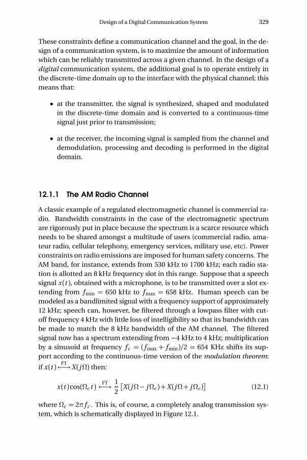
A classic example of a regulated electromagnetic channel is commercial ra-dio. Bandwidth constraints in the case of the electromagnetic spectrumare rigorously put in place because the spectrum is a scarce resource whichneeds to be shared amongst a multitude of users (commercial radio, ama-teur radio, cellular telephony, emergency services, military use, etc). Powerconstraints on radio emissions are imposed for human safety concerns. TheAM band, for instance, extends from 530 kHz to 1700 kHz; each radio sta-tion is allotted an 8 kHz frequency slot in this range. Suppose that a speechsignal x (t ), obtained with a microphone, is to be transmitted over a slot ex-tending from f min = 650 kHz to f max = 658 kHz. Human speech can bemodeled as a bandlimited signal with a frequency support of approximately12 kHz; speech can, however, be filtered through a lowpass filter with cut-off frequency 4 kHz with little loss of intelligibility so that its bandwidth canbe made to match the 8 kHz bandwidth of the AM channel. The filteredsignal now has a spectrum extending from −4 kHz to 4 kHz; multiplicationby a sinusoid at frequency f c = (f max + f min)/2 = 654 KHz shifts its sup-port according to the continuous-time version of the modulation theorem:
if x (t )FT←→X (jΩ) then:
x (t )cos(Ωc t )FT←→ 1
2
�X (jΩ− jΩc )+X (jΩ+ jΩc )
(12.1)
where Ωc = 2π f c . This is, of course, a completely analog transmission sys-tem, which is schematically displayed in Figure 12.1.

330 The Communication Channel
cos(Ωc t )
x (t ) ×
Figure 12.1 A simple AM radio transmitter.
12.1.2 The Telephone Channel
The telephone channel is basically a copper wire connecting two users. Be-cause of the enormous number of telephone posts in the world, only a rel-atively small number of wires is used and the wires are switched betweenusers when a call is made. The telephone network (also known as POTS, anacronym for “Plain Old Telephone System”) is represented schematically inFigure 12.2. Each physical telephone is connected via a twisted pair (i.e. apair of plain copper wires) to the nearest central office (CO); there are a lotof central offices in the network so that each telephone is usually no morethan a few kilometers away. Central offices are connected to each other viathe main lines in the network and the digits dialed by a caller are interpretedby the CO as connection instruction to the CO associated to the called num-ber.
CO Network CO
Figure 12.2 The Plain Old Telephone System (POTS).
To understand the limitations of the telephone channel we have to stepback to the old analog times when COs were made of electromechanicalswitches and the voice signals traveling inside the network were boostedwith simple operational amplifiers. The first link of the chain, the twistedpair to the central office, actually has a bandwidth of several MHz since itis just a copper wire (this is the main technical fact behind ADSL, by the

Design of a Digital Communication System 331
way). Telephone companies, however, used to introduce what are calledloading coils in the line to compensate for the attenuation introduced bythe capacitive effects of longer wires in the network. A side effect of thesecoils was to turn the first link into a lowpass filter with a cutoff frequency ofapproximately 4 kHz so that, in practice, the official passband of the tele-phone channel is limited between f min = 300 Hz and f max = 3000 Hz, for atotal usable positive bandwidth W = 2700 Hz. While today most of the net-work is actually digital, the official bandwidth remains in the order of 8 KHz(i.e. a positive bandwidth of 4 KHz); this is so that many more conversationscan be multiplexed over the same cable or satellite link. The standard sam-pling rate for a telephone channel is nowadays 8 KHz and the bandwidthlimitations are imposed only by the antialiasing filters at the CO, for a maxi-mum bandwidth in excess of W = 3400 Hz. The upper and lower ends of theband are not usable due to possible great attenuations which may take placein the transmission. In particular, telephone lines exhibit a sharp notch atf = 0 (also known as DC level) so that any transmission scheme will have touse bandpass signals exclusively.
The telephone channel is power limited as well, of course, since tele-phone companies are quite protective of their equipment. Generally, thelimit on signaling over a line is 0.2 V rms; the interesting figure howeveris not the maximum signaling level but the overall signal-to-noise ratio ofthe line (i.e. the amount of unavoidable noise on the line with respect tothe maximum signaling level). Nowadays, phone lines are extremely high-quality: a SNR of at least 28 dB can be assumed in all cases and one of 32-34 dB can be reasonably expected on a large percentage of individual con-nections.
12.2 Modem Design: The Transmitter
Data transmission over a physical medium is by definition analog; moderncommunication systems, however, place all of the processing in the digitaldomain so that the only interface with the medium is the final D/A converterat the end of the processing chain, following the signal processing paradigmof Section 9.7.
12.2.1 Digital Modulation and the Bandwidth Constraint
In order to develop a digital communication system over the telephonechannel, we need to re-cast the problem in the discrete-time domain. Tothis end, it is helpful to consider a very abstract view of the data transmitter,

332 Modem Design: The Transmitter
..0110001010...
TX I (t ) s (t )
Fs
s [n ]
Figure 12.3 Abstract view of a digital transmitter.
as shown in Figure 12.3. Here, we neglect the details associated to the dig-ital modulation process and concentrate on the digital-to-analog interface,represented in the picture by the interpolator I (t ); the input to the trans-mitter is some generic binary data, represented as a bit stream. The band-width constraints imposed by the channel can be represented graphicallyas in Figure 12.4. In order to produce a signal which “sits” in the prescribedfrequency band, we need to use a D/A converter working at a frequencyFs ≥ 2f max. Once the interpolation frequency is chosen (and we will seemomentarily the criteria to do so), the requirements for the discrete-timesignal s [n ] are set. The bandwidth requirements become simply
ωmin,max = 2πf min,max
Fs
and they can be represented as in Figure 12.5 (in the figure, for instance, wehave chosen Fs = 2.28 f max).
bandwidth constraint
power constraint
0 Ff min f max Fs
Figure 12.4 Analog specifications (positive frequencies) for the transmitter.
We can now try to understand how to build a suitable s [n ] by lookingmore in detail into the input side of the transmitter, as shown in Figure 12.6.The input bitstream is first processed by a scrambler, whose purpose is torandomize the data; clearly, it is a pseudo-randomization since this opera-tion needs to be undone algorithmically at the receiver. Please note how theimplementation of the transmitter in the digital domain allows for a seam-less integration between the transmission scheme and more abstract data

Design of a Digital Communication System 333
0 πωmin ωmaxωc
ωw
Figure 12.5 Discrete-time specifications (positive frequencies) for Fs = 2.28 f max.
manipulation algorithms such as randomizers. The randomized bitstreamcould already be transmitted at this point; in this case, we would be imple-menting a binary modulation scheme in which the signal s [n ] varies be-tween the two levels associated to a zero and a one, much in the fashion oftelegraphic communications of yore. Digital communication devices, how-ever, allow for a much more efficient utilization of the available bandwidthvia the implementation of multilevel signaling. With this strategy, the bit-stream is segmented in consecutive groups of M bits and these bits selectone of 2M possible signaling values; the set of all possible signaling valuesis called the alphabet of the transmission scheme and the algorithm whichassociates a group of M bits to an alphabet symbol is called the mapper. Wewill discuss practical alphabets momentarily; however, it is important to re-mark that the series of symbols can be complex so that all the signals in theprocessing chain up to the final D/A converter are complex signals.
..0110001010...
Scrambler Mapper
Modulator I (t ) s (t )s [n ]
Figure 12.6 Data stream processing detail.
Spectral Properties of the Symbol Sequence. The mapper producesa sequence of symbols a [n ] which is the actual discrete-time signal whichwe need to transmit. In order to appreciate the spectral properties of this se-

334 Modem Design: The Transmitter
quence consider that, if the initial binary bitstream is a maximum-inform-ation sequence (i.e. if the distribution of zeros and ones looks random and“fifty-fifty”), and with the scrambler appropriately randomizing the inputbitstream, the sequence of symbols a [n ] can be modeled as a stochastici.i.d. process distributed over the alphabet. Under these circumstances, thepower spectral density of the random signal a [n ] is simply
PA (e jω) =σ2A
whereσA depends on the design of the alphabet and on its distribution.
Choice of Interpolation Rate. We are now ready to determine a suit-able rate Fs for the final interpolator. The signal a [n ] is a baseband, fullbandsignal in the sense that it is centered around zero and its power spectral den-sity is nonzero over the entire [−π,π] interval. If interpolated at Fs , such asignal gives rise to an analog signal with nonzero spectral power over theentire [−Fs/2, Fs /2] interval (and, in particular, nonzero power at DC level).In order to fulfill the channel’s constraints, we need to produce a signal witha bandwidth ofωw =ωmax−ωmin centered aroundωc =±(ωmax+ωmin)/2.The “trick” is to upsample (and interpolate) the sequence a [n ], in order tonarrow its spectral support.(1) Assuming ideal discrete-time interpolators,an upsampling factor of 2, for instance, produces a half-band signal; an up-sampling factor of 3 produces a signal with a support spanning one third ofthe total band, and so on. In the general case, we need to choose an upsam-pling factor K so that:
2π
K≤ωw
Maximum efficiency occurs when the available bandwidth is entirely occu-pied by the signal, i.e. when K = 2π/ωw . In terms of the analog bandwidthrequirements, this translates to
K =Fs
f w(12.2)
where f w = f max− f min is the effective positive bandwidth of the transmittedsignal; since K must be an integer, the previous condition implies that wemust choose an interpolation frequency which is a multiple of the positive
(1)A rigorous mathematical analysis of multirate processing of stochastic signals turns outto be rather delicate and beyond the scope of this book; the same holds for the effects ofmodulation, which will appear later on. Whenever in doubt, we may simply visualize theinvolved signals as a deterministic realization whose spectral shape mimics the powerspectral density of their generating stochastic process.

Design of a Digital Communication System 335
passband width f w . The two criteria which must be fulfilled for optimalsignaling are therefore:�
Fs ≥ 2f max
Fs = K f w K ∈� (12.3)
..0110001010...
Scrambler Mapper K ↑a [n ]
G (z ) × Re I (t ) s (t )
e jωc n
b [n ] c [n ] s [n ]
Figure 12.7 Complete digital transmitter.
The Baseband Signal. The upsampling by K operation, used to nar-row the spectral occupancy of the symbol sequence to the prescribed band-width, must be followed by a lowpass filter, to remove the multiple copies ofthe upsampled spectrum; this is achieved by a lowpass filter which, in dig-ital communication parlance, is known as the shaper since it determinesthe time domain shape of the transmitted symbols. We know from Sec-tion 11.2.1 that, ideally, we should use a sinc filter to perfectly remove allrepeated copies. Since this is clearly not possible, let us now examine theproperties that a practical discrete-time interpolator should possess in thecontext of data communications. The baseband signal b [n ] can be expressedas
b [n ] =∑m
a K U [m ] g [n −m ]
where a K U [n ] is the upsampled symbol sequence and g [n ] is the lowpassfilter’s impulse response. Since a K U [n ] = 0 for n not a multiple of K , we canstate that:
b [n ] =∑
i
a [i ] g [n − i K ] (12.4)
It is reasonable to impose that, at multiples of K , the upsampled sequenceb [n ] takes on the exact symbol value, i.e. b [m K ] = a [m ]; this translates tothe following requirement for the lowpass filter:
g [m K ] =
�1 m = 0
0 m �= 0(12.5)

336 Modem Design: The Transmitter
This is nothing but the classical interpolation property which we saw in Sec-tion 9.4.1. For realizable filters, this condition implies that the minimum fre-quency support of G (e jω) cannot be smaller than [−π/K ,π/K ].(2) In otherwords, there will always be a (controllable) amount of frequency leakage out-side of a prescribed band with respect to an ideal filter.
To exactly fullfill (12.5), we need to use an FIR lowpass filter; FIR ap-proximations to a sinc filter are, however, very poor, since the impulse re-sponse of the sinc decays very slowly. A much friendlier lowpass charac-teristic which possesses the interpolation property and allows for a precisequantification of frequency leakage, is the raised cosine. A raised cosine withnominal bandwidth ωw (and therefore with nominal cutoff ωb = ωw /2) isdefined over the positive frequency axis as
G (e jω) =
⎧⎪⎪⎪⎨⎪⎪⎪⎩1 if 0<ω< (1−β )ωb
0 if (1+β )ωb <ω<π1
2+
1
2cos
�πω− (1−β )ωb
2βωb
�if (1−β )ωb <ω< (1+β )ωb
(12.6)
and is symmetric around the origin. The parameter β , with 0 < β < 1, ex-actly defines the amount of frequency leakage as a percentage of the pass-band. The closer β is to one, the sharper the magnitude response; a set offrequency responses forωb =π/2 and various values of β are shown in Fig-ure 12.8. The raised cosine is still an ideal filter but it can be shown that its
0 π-π
0
1
Figure 12.8 Frequency responses of a half-band raised-cosine filter for increasingvalues of β : from black to light gray, β = 0.1, β = 0.2, β = 0.4, β = 0.9.
(2)A simple proof of this fact can be outlined using multirate signal processing. Assumethe spectrum G (e jω) is nonzero only over [−ωb ,ωb ], forωb < π/K ; g [n] can thereforebe subsampled by at least a factor of K without aliasing, and the support of the resultingspectrum is going to be [−Kωb , Kωb ], with Kωb < π. However, g [K n] = δ[n], whosespectral support is [−π,π].

Design of a Digital Communication System 337
impulse response decays as 1/n 3 and, therefore, good FIR approximationscan be obtained with a reasonable amount of taps using a specialized ver-sion of Parks-McClellan algorithm. The number of taps needed to achieve agood frequency response obviously increases as β approaches one; in mostpractical applications, however, it rarely exceeds 50.
The Bandpass Signal. The filtered signal b [n ] = g [n ] ∗ a K U [n ] is now abaseband signal with total bandwidth ωw . In order to shift the signal intothe allotted frequency band, we need to modulate(3) it with a sinusoidal car-rier to obtain a complex bandpass signal:
c [n ] = b [n ]e jωc n
where the modulation frequency is the center-band frequency:
ωc =ωmin+ωmax
2
Note that the spectral support of the modulated signal is just the positiveinterval [ωmin,ωmax]; a complex signal with such a one-sided spectral occu-pancy is called an analytic signal. The signal which is fed to the D/A con-verter is simply the real part of the complex bandpass signal:
s [n ] =Re�
c [n ]�
(12.7)
If the baseband signal b [n ] is real, then (12.7) is equivalent to a standardcosine modulation as in (12.1); in the case of a complex b [n ] (as in our case),the bandpass signal is the combination of a cosine and a sine modulation,which we will examine in more detail later. The spectral characteristics ofthe signals involved in the creation of s [n ] are shown in Figure 12.9.
Baud Rate vs Bit Rate. The baud rate of a communication system is thenumber of symbols which can be transmitted in one second. Consideringthat the interpolator works at Fs samples per second and that, because ofupsampling, there are exactly K samples per symbol in the signal s [n ], thebaud rate of the system is
B =Fs
K= f w (12.8)
where we have assumed that the shaper G (z ) is an ideal lowpass. As a gen-eral rule, the baud rate is always smaller or equal to the positive passbandof the channel. Moreover, if we follow the normal processing order, we can
(3)See footnote (1).

338 Modem Design: The Transmitter
0 π-π ωmin ωmaxωc−ωc
0 π-π ωmin ωmaxωc−ωc
0 π-π ωmin ωmaxωc−ωc
Figure 12.9 Construction of the modulated signal: PSD of the symbol sequencea [n ] (top panel); PSD of the upsampled and shaped signal b [n ] (middle panel);PSD of the real modulated signal s [n ] (bottom panel). The channel’s bandwidthrequirements are indicated by the dashed areas.
equivalently say that a symbol sequence generated at B symbols per secondgives rise to a modulated signal whose positive passband is no smaller thanB Hz. The effective bandwidth f w depends on the modulation scheme and,especially, on the frequency leakage introduced by the shaper.
Design of a Digital Communication System 339
The total bit rate of a transmission system, on the other hand, is at mostthe baud rate times the log in base 2 of the number of symbols in the alpha-bet; for a mapper which operates on M bits per symbol, the overall bitrateis
R =M B (12.9)
A Design Example. As a practical example, consider the case of a tele-phone line for which f min = 450 Hz and f max = 3150 Hz (we will considerthe power constraints later). The baud rate can be at most 2700 symbols persecond, since f w = f max − f min = 2700 Hz. We choose a factor β = 0.125 forthe raised cosine shaper and, to compensate for the bandwidth expansion,we deliberately reduce the actual baud rate to B = 2700/(1+β ) = 2400 sym-bols per second, which leaves the effective positive bandwidth equal to f w .The criteria which the interpolation frequency must fulfill are therefore thefollowing:�
Fs ≥ 2f max = 6300
Fs = K B = 2400 K K ∈�The first solution is for K = 3 and therefore Fs = 7200. With this inter-polation frequency, the effective bandwidth of the discrete-time signal isωw = 2π(2700/7200) = 0.75π and the carrier frequency for the bandpasssignal is ωc = 2π(450+ 3150)/(2Fs ) = π/2. In order to determine the maxi-mum attainable bitrate of this system, we need to address the second majorconstraint which affects the design of the transmitter, i.e. the power con-straint.
12.2.2 Signaling Alphabets and the Power Constraint
The purpose of the mapper is to associate to each group of M input bits avalue α from a given alphabet� . We assume that the mapper includes amultiplicative factor G0 which can be used to set the final gain of the gen-erated signal, so that we don’t need to concern ourselves with the absolutevalues of the symbols in the alphabet; the symbol sequence is therefore:
a [n ] =G0α[n ], α[n ]∈�and, in general, the values α are set at integer coordinates out of conve-nience.
Transmitted Power. Under the above assumption of an i.i.d. uniformlydistributed binary input sequence, each group of M bits is equally probable;since we consider only memoryless mappers, i.e. mappers in which no de-

340 Modem Design: The Transmitter
pendency between symbols is introduced, the mapper acts as the source ofa random process a [n ]which is also i.i.d. The power of the output sequencecan be expressed as
σ2a = E
��a [n ]��2=G 2
0
∑α∈�
��α��2pa (α) (12.10)
=G 20σ
2α (12.11)
where pa (α) is the probability assigned by the mapper to symbol α ∈ � ;the distribution over the alphabet� is one of the design parameters of themapper, and is not necessarily uniform. The variance σ2
α is the intrinsicpower of the alphabet and it depends on the alphabet size (it increases ex-ponentially with M ), on the alphabet structure, and on the probability dis-tribution of the symbols in the alphabet. Note that, in order to avoid wast-ing transmission energy, communication systems are designed so that thesequence generated by the mapper is balanced, i.e. its DC value is zero:
E[α[n ]]=∑α∈�αpa (α) = 0
Using (8.25), the power of the transmitted signal, after upsampling and mod-ulation, is
σ2s =
1
π
∫ ωmax
ωmin
1
2
��G (e jω)��2G 2
0σ2α (12.12)
The shaper is designed so that its overall energy over the passband is G 2 =2π and we can express this as follows:
σ2s =G 2
0σ2α (12.13)
In order to respect the power constraint, we have to choose a value for G0
and design an alphabet� so that:
σ2s ≤ Pmax (12.14)
where Pmax is the maximum transmission power allowed on the channel.The goal of a data transmission system is to maximize the reliable through-put but, unfortunately, in this respect the parameters σ2
α and G0 act uponconflicting priorities. If we use (12.9) and boost the transmitter’s bitrate byincreasing M , then σ2
α grows and we must necessarily reduce the gain G0
to fulfill the power constraint; but, in so doing, we impair the reliability ofthe transmission. To understand why that is, we must leap ahead and con-sider both a practical alphabet and the mechanics of symbol decoding at thetransmitter.

Design of a Digital Communication System 341
QAM. The simplest mapping strategies are one-to-one correspondencesbetween binary values and signal values: note that in these cases the sym-bol sequence is uniformly distributed with pa (α) = 2−M for all α ∈ � . Forexample, we can assign to each group of M bits (b0, . . . ,bM−1) the signed bi-nary number b0b1b2 · · ·bM−1 which is a value between −2M−1 and 2M−1 (b0
is the sign bit). This signaling scheme is called pulse amplitude modula-tion (PAM) since the amplitude of each transmitted symbol is directly deter-mined by the binary input value. The PAM alphabet is clearly balanced andthe inherent power of the mapper’s output is readily computed as(4)
σ2α =
2M−1∑α=1
2−Mα2 =2M (2M + 3)+ 2
24
Now, a pulse-amplitude modulated signal prior to modulation is a base-band signal with positive bandwidth of, say, ω0 (see Figure 12.9, middlepanel); therefore, the total spectral support of the baseband PAM signal is2ω0. After modulation, the total spectral support of the signal actually dou-bles (Fig. 12.9, bottom panel); there is, therefore, some sort of redundancyin the modulated signal which causes an underutilization of the availablebandwidth. The original spectral efficiency can be regained with a signalingscheme called quadrature amplitude modulation (QAM); in QAM the sym-bols in the alphabet are complex quantities, so that two real values are trans-mitted simultaneously at each symbol interval. Consider a complex symbolsequence
a [n ] =G0�αI [n ]+ j αQ [n ]
�= a I [n ]+ j aQ [n ]
Since the shaper is a real-valued filter, we have that:
b [n ] =�
a I ,K U ∗ g [n ]�+ j�
aQ ,K U ∗ g [n ]�= bI [n ]+ j bQ [n ]
so that, finally, (12.7) becomes:
s [n ] =Re�
b [n ]e jωc n�
=b I [n ]cos(ωc n )−bQ [n ]sin(ωc n )
In other words, a QAM signal is simply the linear combination of two pulse-amplitude modulated signals: a cosine carrier modulated by the real part ofthe symbol sequence and a sine carrier modulated by the imaginary part ofthe symbol sequence. The sine and cosine carriers are orthogonal signals,so that b I [n ] and bQ [n ] can be exactly separated at the receiver via a sub-space projection operation, as we will see in detail later. The subscripts I
(4)A useful formula, here and in the following, is∑N
n=1 n 2 =N (N +1)(2N +1)/6.
342 Modem Design: The Transmitter
and Q derive from the historical names for the cosine carrier (the in-phasecarrier) and the sine carrier which is the quadrature (i.e. the orthogonal car-rier). Using complex symbols for the description of the internal signals inthe transmitter is an abstraction which simplifies the overall notation andhighlights the usefulness of complex discrete-time signal models.
1
2
3
4
-1
-2
-3
-4
1 2 3 4-1-2-3-4 Re
Im
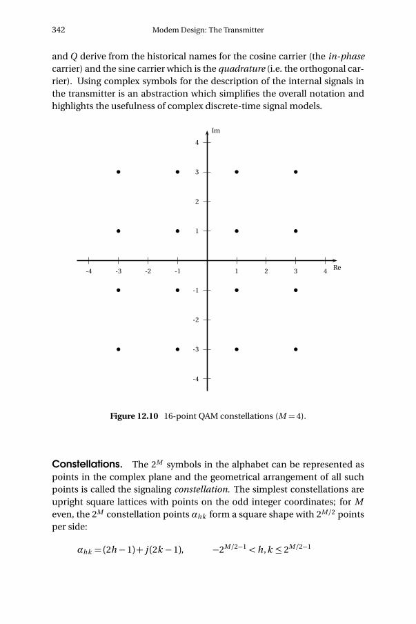
Figure 12.10 16-point QAM constellations (M = 4).
Constellations. The 2M symbols in the alphabet can be represented aspoints in the complex plane and the geometrical arrangement of all suchpoints is called the signaling constellation. The simplest constellations areupright square lattices with points on the odd integer coordinates; for Meven, the 2M constellation points αhk form a square shape with 2M/2 pointsper side:
αhk = (2h − 1)+ j (2k − 1), −2M/2−1 < h,k ≤ 2M/2−1
Design of a Digital Communication System 343
Such square constellations are called regular and a detailed example isshown in Figure 12.10 for M = 4; other examples for M = 2,6,8 are shownin Figure 12.11. The nominal power associated to a regular, uniformly dis-tributed constellation on the square lattice can be computed as the secondmoment of the points; exploiting the fourfold symmetry, we have
σ2α = 4
2M/2−1∑h=1
2M/2−1∑k=1
2−M�
2h − 1�2+
�2k − 1
�2�=
2
3(2M − 1) (12.15)
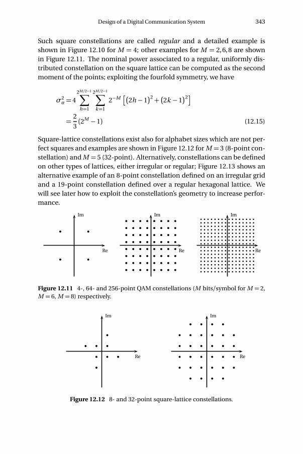
Square-lattice constellations exist also for alphabet sizes which are not per-fect squares and examples are shown in Figure 12.12 for M = 3 (8-point con-stellation) and M = 5 (32-point). Alternatively, constellations can be definedon other types of lattices, either irregular or regular; Figure 12.13 shows analternative example of an 8-point constellation defined on an irregular gridand a 19-point constellation defined over a regular hexagonal lattice. Wewill see later how to exploit the constellation’s geometry to increase perfor-mance.
Re
Im
Re
Im
Re
Im
Figure 12.11 4-, 64- and 256-point QAM constellations (M bits/symbol for M = 2,M = 6, M = 8) respectively.
Re
Im
Re
Im
Figure 12.12 8- and 32-point square-lattice constellations.

344 Modem Design: The Transmitter
Re
Im
Re
Im
Figure 12.13 More exotic constellations: irregular low-power 8-point constellation(left panel) in which the outer point are at a distance of 1+
�3 from the origin ;
regular 19-point hexagonal-lattice constellation (right panel).
Transmission Reliability. Let us assume that the receiver has eliminatedall the “fixable” distortions introduced by the channel so that an “almostexact” copy of the symbol sequence is available for decoding; call this se-quence a [n ]. What no receiver can do, however, is eliminate all the additivenoise introduced by the channel so that:
a [n ] = a [n ]+η[n ] (12.16)
where η[n ] is a complex white Gaussian noise term. It will be clear later whythe internal mechanics of the receiver make it easier to consider a complexrepresentation for the noise; again, such complex representation is a conve-nient abstraction which greatly simplifies the mathematical analysis of thedecoding process. The real-valued zero-mean Gaussian noise introduced bythe channel, whose variance is σ2
0, is transformed by the receiver into com-plex Gaussian noise whose real and imaginary parts are independent zero-mean Gaussian variables with variance σ2
0/2. Each complex noise sampleη[n ] is distributed according to
fη(z ) =1
πσ20
e− |z |2σ2
0 (12.17)
The magnitude of the noise samples introduces a shift in the complexplane for the demodulated symbols a [n ]with respect to the originally trans-mitted symbols; if this displacement is too big, a decoding error takes place.In order to quantify the effects of the noise we have to look more in detailat the way the transmitted sequence is retrieved at the receiver. A boundon the probability of error can be obtained analytically if we consider a sim-ple QAM decoding technique called hard slicing. In hard slicing, a valuea [n ] is associated to the most probable symbol α ∈ � by choosing the al-phabet symbol at the minimum Euclidean distance (taking the gain G0 intoaccount):

Design of a Digital Communication System 345
��a [n ]�= arg min
α∈����a [n ]−G0α
��2�The hard slicer partitions the complex plane into decision regions centeredon alphabet symbols; all the received values which fall into the decision re-gion centered on α are mapped back onto α. Decision regions for a 16-pointconstellation, together with examples of correct and incorrect hard slicingare represented in Figure 12.14: when the error sample η[n ] moves the re-ceived symbol outside of the right decision region, we have a decoding er-ror. For square-lattice constellations, this happens when either the real orthe imaginary part of the noise sample is larger than the minimum distancebetween a symbol and the closest decision region boundary. Said distanceis d min =G0, as can be easily seen from Figure 12.10, and therefore the prob-ability of error at the receiver is
pe = 1−P��
Re�η[n ]
�<G0
�∧�
Im�η[n ]
�<G0
� = 1−
∫D
fη(z )d z
Re
Im
��
��
��
��
��
��
��
��
��
��
��
��
��
��
��
��
*
Re
Im
��
��
��
��
��
��
��
��
��
��
��
��
��
��
��
��
*
Figure 12.14 Decoding of noisy symbols: transmitted symbol is black dot, receivedvalue is the star. Correct decoding (left) and decoding error (right).
where fη(x ) is the pdf of the additive complex noise and D is a square onthe complex plane centered at the origin and 2d min wide. We can obtaina closed-form expression for the probability of error if we approximate thedecision region D by the inscribed circle of radius d min (Fig. 12.15), so:
pe = 1−∫|z |<G0
fη(z )d z
= 1−∫ 2π
0
dθ
∫ G0
0
ρ
πσ20
e− ρ2
σ20
= e−G 2
0σ2
0 (12.18)

346 Modem Design: The Transmitter
where we have used (12.17) and the change of variable z =ρ e j θ . The prob-ability of error decreases exponentially with the gain and, therefore, with thepower of the transmitter.
G0
�� �� ��
�� ��
�� �� ��
Figure 12.15 Decision region and its circular approximation.
The concept of “reliability” is quantified by the probability of error thatwe are willing to tolerate; note that this probability can never be zero, butit can be made arbitrarily low – values on the order of pe = 10−6 are usuallytaken as a reference. Assume that the transmitter transmits at the maxi-mum permissible power so that the SNR on the channel is maximized. Un-der these conditions it is
SNR=σ2
s
σ20
=G 20
σ2α
σ20
and from (12.18) we have
SNR=− ln(pe )σ2α (12.19)
For a regular square-lattice constellation we can use (12.15) to determinethe maximum number of bits per symbol which can be transmitted at thegiven reliability figure:
M = log2
�1− 3
2
SNR
ln(pe )
�(12.20)

Design of a Digital Communication System 347
and this is how the power constraint ultimately affects the maximum achiev-able bitrate. Note that the above derivation has been carried out with veryspecific hypotheses on both the signaling alphabet and on the decoding al-gorithm (the hard slicing); the upper bound on the achievable rate on thechannel is actually a classic result of information theory and is known un-der the name of Shannon’s capacity formula. Shannon’s formula reads
C = B log2
�1+
S
N
�where C is the absolute maximum capacity in bits per second, B is the avail-able bandwidth in Hertz and S/N is the signal to noise ratio.
Design Example Revisited. Let us resume the example on page 339 byassuming that the power constraint on the telephone line limits the max-imum achievable SNR to 22 dB. If the acceptable bit error probability ispe = 10−6, Equation (12.20) gives us a maximum integer value of M = 4 bitsper symbol. We can therefore use a regular 16-point square constellation;recall we had designed a system with a baud rate of 2400 symbols per sec-ond and therefore the final reliable bitrate is R = 9600 bits per second. Thisis actually one of the operating modes of the V.32 ITU-T modem standard.(5)
12.3 Modem Design: The Receiver
The analog signal s (t ) created at the transmitter is sent over the telephonechannel and arrives at the receiver as a distorted and noise-corrupted signals (t ). Again, since we are designing a purely digital communication system,the receiver’s input interface is an A/D converter which, for simplicity, weassume, is operating at the same frequency Fs as the transmitter’s D/A con-verter. The receiver tries to undo the impairments introduced by the chan-nel and to demodulate the received signal; its output is a binary sequencewhich, in the absence of decoding errors, is identical to the sequence in-jected into the transmitter; an abstract view of the receiver is shown in Fig-ure 12.16.
s (t ) RX..0110001010...
Fs
s [n ]
Figure 12.16 Abstract view of a digital receiver.
(5)ITU-T is the Standardization Bureau of the International Telecommunication Union.

348 Modem Design: The Receiver
12.3.1 Hilbert Demodulation
Let us assume for the time being that transmitter and receiver are connectedback-to-back so that we can neglect the effects of the channel; in this cases (t ) = s (t ) and, after the A/D module, s [n ] = s [n ]. Demodulation of theincoming signal to a binary data stream is achieved according to the blockdiagram in Figure 12.17 where all the steps in the modulation process areundone, one by one.
H (z ) e−jωc n
s (t ) � + ×
j
s [n ] c [n ] b [n ]
K ↓ Slicer Descrambler..0110001010...
a [n ]
Figure 12.17 Complete digital receiver.
The first operation is retrieving the complex bandpass signal c [n ] fromthe real signal s [n ]. An efficient way to perform this operation is by ex-ploiting the fact that the original c [n ] is an analytic signal and, therefore,its imaginary part is completely determined by its real part. To see this,consider a complex analytic signal x [n ], i.e. a complex sequence for whichX (e jω) = 0 over the [−π,0] interval (with the usual 2π-periodicity, obvi-ously). We can split x [n ] into real and imaginary parts:
x [n ] = xr [n ]+ j xi [n ]
so that we can write:
xr [n ] =x [n ]+x ∗[n ]
2
xi [n ] =x [n ]−x ∗[n ]
2j
In the frequency domain, these relations translate to (see (4.46)):
Xr (e jω) =�
X (e jω)+X ∗(e−jω)
2(12.21)
Xi (e jω) =�
X (e jω)−X ∗(e−jω)
2j (12.22)

Design of a Digital Communication System 349
0 π-π
0
1
0 π-π
0
1
Figure 12.18 Magnitude spectrum of an analytic signal x [n ].��X ∗(e−jω)
�� (left) and��X ∗(e−jω)�� (right).
Since x [n ] is analytic, by definition X (e jω) = 0 for −π≤ω< 0, X ∗(e−jω) = 0for 0<ω≤π and X (e jω) does not overlap with X ∗(e−jω) (Fig. 12.18). We cantherefore use (12.21) to write:
X (e jω) =
�2Xr (e jω) for 0≤ω≤π0 for−π<ω< 0
(12.23)
Now, xr [n ] is a real sequence and therefore its Fourier transform is conjugate-symmetric, i.e. Xr (e jω) = X ∗r (e−jω); as a consequence
X ∗(e−jω) =
�0 for 0≤ω≤π2Xr (e jω) for−π<ω< 0
(12.24)
By using (12.23) and (12.24) in (12.22) we finally obtain:
Xi (e jω) =
�−j Xr (e jω) for 0≤ω≤π+j Xr (e jω) for −π<ω< 0
(12.25)
which is the product of Xr (e jω) with the frequency response of a Hilbertfilter (Sect. 5.6). In the time domain this means that the imaginary part of ananalytic signal can be retrieved from the real part only via the convolution:
xi [n ] = h[n ] ∗xr [n ]
At the demodulator, s [n ] = s [n ] is nothing but the real part of c [n ] andtherefore the analytic bandpass signal is simply
c [n ] = s [n ]+ j�h[n ] ∗ s [n ]
�In practice, the Hilbert filter is approximated with a causal, 2L+ 1-tap typeIII FIR, so that the structure used in demodulation is that of Figure 12.19.

350 Modem Design: The Receiver
H (z )
s [n ] � + c [n − L]
z−L
j
Figure 12.19 Retrieving the complex baseband signal with an FIR Hilbert filter ap-proximation.
The delay in the bottom branch compensates for the delay introduced bythe causal filter and puts the real and derived imaginary part back in sync toobtain:
c [n ] = s [n − L]+ j�h[n ] ∗ s [n ]
�Once the analytic bandpass signal is reconstructed, it can be brought
back to baseband via a complex demodulation with a carrier with frequency−ωc :
b [n ] = c [n ]e−jωc n
Because of the interpolation property of the pulse shaper, the sequence ofcomplex symbols can be retrieved by a simple downsampling-by-K opera-tion:
a [n ] = b [n K ]
Finally, the slicer (which we saw in Section 12.2.2) associates a group of Mbits to each received symbol and the descrambler reconstructs the originalbinary stream.
12.3.2 The Effects of the Channel
If we now abandon the convenient back-to-back scenario, we have to dealwith the impairments introduced by the channel and by the signal process-ing hardware. The telephone channels affects the received signal in threefundamental ways:
• it adds noise to the signal so that, even in the best case, the signal-to-noise ratio of the received signal cannot exceed a maximum limit;
• it distorts the signal, acting as a linear filter;
• it delays the signal, according to the propagation time from transmit-ter to receiver.
Design of a Digital Communication System 351
Distortion and delay are obviously both linear transformations and, as such,their description could be lumped together; still, the techniques which dealwith distortion and delay are different, so that the two are customarily keptseparate. Furthermore, the physical implementation of the devices intro-duces an unavoidable lack of absolute synchronization between transmit-ter and receiver, since each of them runs on an independent internal clock.Adaptive synchronization becomes a necessity in all real-world devices, andwill be described in the next Section.
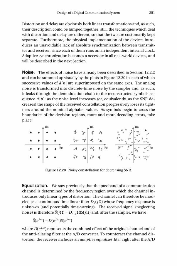
Noise. The effects of noise have already been described in Section 12.2.2and can be summed up visually by the plots in Figure 12.20 in each of whichsuccessive values of a [n ] are superimposed on the same axes. The analognoise is transformed into discrete-time noise by the sampler and, as such,it leaks through the demodulation chain to the reconstructed symbols se-quence a [n ]; as the noise level increases (or, equivalently, as the SNR de-creases) the shape of the received constellation progressively loses its tight-ness around the nominal alphabet values. As symbols begin to cross theboundaries of the decision regions, more and more decoding errors, takeplace.
Re
Im
*
*
*
*
*
*
*
*
*
*
*
*
*
*
*
*
*
*
*
*
*
*
*
*
*
*
*
*
*
*
*
*
*
*
*
*
*
*
*
*
*
*
*
*
*
*
*
*
*
*
*
*
*
*
*
*
*
*
*
*
*
*
*
*
*
*
*
*
*
*
*
*
*
*
*
*
*
*
*
*
Re
Im
*
*
*
*
*
*
*
*
*
*
*
*
*
*
*
*
*
*
*
*
*
*
*
*
*
*
*
*
*
*
*
*
*
*
*
*
*
*
*
*
*
*
*
*
*
*
*
*
*
*
*
*
*
*
*
*
*
*
*
*
*
*
*
*
*
*
*
*
*
*
*
*
*
*
*
*
*
*
*
*
Re
Im
*
*
*
*
*
**
*
*
*
*
*
*
*
*
*
*
*
*
*
*
*
*
*
*
*
*
*
*
*
*
*
*
*
*
*
*
*
*
*
*
*
*
*
*
*
*
*
*
*
*
*
*
**
*
*
*
*
*
*
**
*
*
*
*
*
*
*
*
*
*
*
**
*
*
*
*
Figure 12.20 Noisy constellation for decreasing SNR.
Equalization. We saw previously that the passband of a communicationchannel is determined by the frequency region over which the channel in-troduces only linear types of distortion. The channel can therefore be mod-eled as a continuous-time linear filter Dc (jΩ) whose frequency response isunknown (and potentially time-varying). The received signal (neglectingnoise) is therefore S(jΩ)=Dc (jΩ)S(jΩ) and, after the sampler, we have
S(e jω) =D(e jω)S(e jω)
where D(e jω) represents the combined effect of the original channel and ofthe anti-aliasing filter at the A/D converter. To counteract the channel dis-tortion, the receiver includes an adaptive equalizer E (z ) right after the A/D

352 Modem Design: The Receiver
converter; this is an FIR filter which is modified on the fly so that E (z ) ≈1/D(z ). While adaptive filter theory is beyond the scope of this book, theintuition behind adaptive equalization is shown in Figure 12.21. In fact, thedemodulator contains an exact copy of the modulator as well; if we assumethat the symbols produced by the slicer are error-free, a perfect copy of thetransmitted signal s [n ] can be generated locally at the receiver. The differ-ence between the equalized signal and the reconstructed original signal isused to adapt the taps of the equalizer so that:
d [n ] = s e [n ]− s [n ]−→ 0
Clearly, in the absence of a good initial estimate for D(e jω), the sliced val-ues a [n ] are nothing like the original sequence; this is obviated by havingthe transmitter send a pre-established training sequence which is known inadvance at the receiver. The training sequence, together with other syn-chronization signals, is sent each time a connection is established betweentransmitter and receiver and is part of the modem’s handshaking protocol.By using a training sequence, E (z ) can quickly converge to an approxima-tion of 1/D(z ) which is good enough for the receiver to start decoding sym-bols correctly and use them in driving further adaptation.
s [n ] E (z ) � Demod Slicer �
− Modulator
s e [n ] a [n ]
s [n ]d [n ]
Figure 12.21 Adaptive equalization: based on the estimated symbols the receivercan synthesize the perfect desired equalizer output and use the difference to drivethe adaptation.
Delay. The continuous-time signal arriving at the receiver can be modeledas
s (t ) = (s ∗ v )(t − td )+η(t ) (12.26)
where v (t ) is the continuous-time impulse response of the channel, η(t ) isthe continuous-time noise process and td is the propagation delay, i.e. thetime it takes for the signal to travel from transmitter to receiver. After thesampler, the discrete-time signal to be demodulated is s [n ] = s (nTs ); if weneglect the noise and distortion, we can write
s [n ] = s (nTs − td ) = s�(n −n d )Ts −τTs
�(12.27)

Design of a Digital Communication System 353
where we have split the delay as td = (n d +τ)Ts with n d ∈ � and |τ| ≤ 1/2.The term n d is called the bulk delay and it can be estimated easily in a full-duplex system by the following handshaking procedure:
1. System A sends an impulse to system B at time n = 0; the impulseappears on the channel after a known processing delay tp 1 seconds;let the (unknown) channel propagation delay be td seconds.
2. System B receives the impulse and sends an impulse back to A; theprocessing time tp 2 (decoding of the impulse and generation of re-sponse) is known by design.
3. The response impulse is received by system A after td seconds (prop-agation delay is symmetric) and detected after a processing delay oftp 3 seconds.
In the end, the total round-trip delay measured by system A is
t = 2td + tp 1+ tp 2+ tp 3= 2td + tp
since tp is known exactly in terms of the number of samples, td can be esti-mated to within a sample. The bulk delay is easily dealt with at the receiver,since it translated to a simple z−n d component in the channel’s response.The fractional delay, on the other hand, is a more delicate entity which wewill need to tackle with specialized machinery.
12.4 Adaptive Synchronization
In order for the receiver to properly decode the data, the discrete-timesignals inside the receiver must be synchronous with the discrete-time sig-nals generated by the transmitter. In the back-to-back operation, we couldneglect synchronization problems since we assumed s [n ] = s [n ]. In reality,we will need to compensate for the propagation delay and for possible clockdifferences between the D/A at the transmitter and the A/D at the receiver,both in terms of time offsets and in terms of frequency offsets.
12.4.1 Carrier Recovery
Carrier recovery is the modem functionality by which any phase offset be-tween carriers is estimated and compensated for. Phase offsets between thetransmitter’s and receiver’s carriers are due to the propagation delay and tothe general lack of a reference clock between the two devices. Assume that

354 Adaptive Synchronization
the oscillator in the receiver has a phase offset of θ with respect to the trans-mitter; when we retrieve the baseband signal b [n ] from c [n ] we have
b [n ] = c [n ]e−j (ωc n−θ ) = c [n ]e−j (ωc n−θ ) = b [n ]e j θ
where we have neglected both distortion and noise and assumed c [n ] =c [n ]. Such a phase offset translates to a rotation of the constellation pointsin the complex plane since, after downsampling, we have a [n ] = a [n ]e j θ .Visually, the received constellation looks like in Figure 12.22, where θ =π/20= 9◦. If we look at the decision regions plotted in Figure 12.22, it is clearthat in the rotated constellation some points are shifted closer to the deci-sion boundaries; for these, a smaller amount of noise is sufficient to causeslicing errors. An even worse situation happens when the receiver’s carrierfrequency is slightly different than the transmitter’s carrier frequency; in thiscase the phase offset changes over time and the points in the constellationstart to rotate with an angular speed equal to the difference between fre-quencies. In both cases, data transmission becomes highly unreliable: car-rier recovery is then a fundamental part of modem design.
Re
Im
��
��
��
��
��
��
��
��
��
��
��
��
��
��
��
��
Figure 12.22 Rational effect of a phase offset on the received symbols.
The most common technique for QAM carrier recovery over well-behaved channels is a decision directed loop; just as in the case of the adap-tive equalizer, this works when the overall SNR is sufficiently high and thedistortion is mild so that the slicer’s output is an almost error-free sequenceof symbols. Consider a system with a phase offset of θ ; in Figure 12.23 the

Design of a Digital Communication System 355
Re
Im
*
a 1
a 2
Figure 12.23 Estimation of the phase offset.
rotated symbol α (indicated by a star) is sufficiently close to the transmittedvalue α (indicated by a dot) to be decoded correctly. In the z plane, con-sider the two vectors a 1 and a 2, from the origin to α and α respectively; themagnitude of their vector product can be expressed as�� a 1× a 2
��=Re�α�
Im�α�− Im
�α�
Re�α�
(12.28)
Moreover, the angle between the vectors is θ and it can be computed as�� a 1× a 2
��= �� a 1
�� �� a 2
��sin(θ ) (12.29)
We can therefore obtain an estimate for the phase offset:
sin(θ ) =Re�α�
Im�α�− Im
�α�
Re�α�
| a 1| | a 2| (12.30)
For small angles, we can invoke the approximation sin(θ ) ≈ θ and obtain aquick estimate of the phase offset. In digital systems, oscillators are realizedusing the algorithm we saw in Section 2.1.3; it is easy to modify such a rou-tine to include a time-varying corrective term derived from the estimate of θabove so that the resulting phase offset is close to zero. This works also in thecase of a slight frequency offset, with θ converging in this case to a nonzeroconstant. The carrier recovery block diagram is shown in Figure 12.24.
This decision-directed feedback method is almost always able to “lock”the constellation in place; due to the fourfold symmetry of regular square

356 Adaptive Synchronization
constellations, however, there is no guarantee that the final orientation ofthe locked pattern be the same as the original. This difficulty is overcomeby a mapping technique called differential encoding; in differential encod-ing the first two bits of each symbol actually encode the quadrant offset ofthe symbol with respect to the previous one, while the remaining bits indi-cate the actual point within the quadrant. In so doing, the encoded symbolsequence becomes independent of the constellation’s absolute orientation.
s [n ] E (z ) Demod � Slicer �
e jωc n −
a [n ] a [n ]
Figure 12.24 Carrier recovery by decision-directed loop.
12.4.2 Timing Recovery
Timing recovery is the ensemble of strategies which are put in place to re-cover the synchronism between transmitter and receiver at the level ofdiscrete-time samples. This synchronism, which was one of the assump-tions of back-to-back operation, is lost in real-world situations because ofpropagation delays and because of slight hardware differences between de-vices. The D/A and A/D, being physically separate, run on independentclocks which may exhibit small frequency differences and a slow drift. Thepurpose of timing recovery is to offset such hardware discrepancies in thediscrete-time domain.
A Digital PLL. Traditionally, a Phase-Locked-Loop (PLL) is an analog cir-cuit which, using a negative feedback loop, manages to keep an internal os-cillator “locked in phase” with an external oscillatory input. Since the in-ternal oscillator’s parameters can be easily retrieved, PLLs are used to accu-rately measure the frequency and the phase of an external signal with re-spect to an internal reference.
In timing recovery, we use a PLL-like structure as in Figure 12.25 to com-pensate for sampling offsets. To see how this PLL works, assume that thediscrete-time samples s [n ] are obtained by the A/D converter as
s [n ] = s (tn ) (12.31)
where the sequence of sampling instants tn is generated as
tn+1 = tn +T [n ] (12.32)

Design of a Digital Communication System 357
sin(2π f 0t +θ ) � sin(2πn/N )
� N ↓tn
Figure 12.25 A digital PLL with a sinusoidal input.
Normally, the sampling period is a constant and T [n ] = Ts = 1/Fs but herewe will assume that we have a special A/D converter for which the samplingperiod can be dynamically changed at each sampling cycle. Assume the in-put to the sampler is a zero-phase sinusoid of known frequency f 0 = Fs /Nfor N ∈� and N ≥ 2:
x (t ) = sin(2π f 0t )
If the sampling period is constant and equal to Ts and if the A/D is syn-chronous to the sinusoid, the sampled signal are simply:
x [n ] = sin�2π
Nn�
We can test such synchronicity by downsampling x [n ] by N and we shouldhave xN D [n ] = 0 for all n ; this situation is shown at the top of Figure 12.26and we can say that the A/D is locked to the reference signal x (t ).
If the local clock has a time lag τ with respect to the reference time ofthe incoming sinusoid (or, alternatively, if the incoming sinusoid is delayedby τ), then the discrete-time, downsampled signal is the constant:
xN D [n ] = sin(2π f 0τ) (12.33)
Note, the A/D is still locked to the reference signal x (t ), but it exhibits aphase offset, as shown in Figure 12.26, middle panel. If this offset is suf-ficiently small then the small angle approximation for the sine holds andxN D [n ] provides a direct estimate of the corrective factor which needs to beinjected into the A/D block. If the offset is estimated at time n 0, it will sufficeto set
T [n ] =
�Ts −τ for n = n 0
Ts for n > n 0(12.34)
for the A/D to be locked to the input sinusoid.

358 Adaptive Synchronization
0
1
-1
�� �� �� ��
0
1
-1
�� �� �� ��
0
1
-1
��
��
��
��
Figure 12.26 Timing recovery from a continuous-time sinusoid, with referencesamples drawn as white circles: perfect locking (top); phase offset (middle) andfrequency drift (bottom). All plots are in the time reference of the input sinusoid.
Suppose now that the the A/D converter runs slightly slower than itsnominal speed or, in other words, that the effective sampling frequency isF ′s = βFs , with β < 1. As a consequence the sampling period is T ′s = Ts/β >
Ts and the discrete-time, downsampled signal becomes
xN D [n ] = sin�(2πβ )n
�(12.35)

Design of a Digital Communication System 359
i.e. it is a sinusoid of frequency 2πβ ; this situation is shown in the bottompanel of Figure 12.26. We can use the downsampled signal to estimate β andwe can re-establish a locked PLL by setting
T [n ] =Ts
β(12.36)
The same strategy can be employed if the A/D runs faster than normal, inwhich case the only difference is that β > 1.
A Variable Fractional Delay. In practice, A/D converters with “tunable”sampling instants are rare and expensive because of their design complex-ity; furthermore, a data path from the discrete-time estimators to the analogsampler would violate the digital processing paradigm in which all of thereceiver works in discrete time and the one-way interface from the analogworld is the A/D converter. In other words: the structure in Figure 12.25 isnot a truly digital PLL loop; to implement a completely digital PLL structure,the adjustment of the sampling instants must be performed in discrete timevia the use of a programmable fractional delay.
Let us start with the case of a simple time-lag compensation for acontinuous-time signal x (t ). Of the total delay td , we assume that the bulkdelay has been correctly estimated so that the only necessary compensationis that of a fractional delay τ, with |τ| ≤ 1/2. From the available sampled sig-nal x [n ] = x (nTs )we want to obtain the signal
xτ[n ] = x (nTs +τTs ) (12.37)
using discrete-time processing only. Since we will be operating in discretetime, we can assume Ts = 1 with no loss of generality and so we can writesimply:
xτ[n ] = x (n +τ)
We know from Section 9.7.2 that the “ideal” way to obtain xτ[n ] fromx [n ] is to use a fractional delay filter:
xτ[n ] = dτ[n ] ∗x [n ]
where Dτ(e jω) = e jωτ. We have seen that the problem with this approach isthat Dτ(e jω) is an ideal filter, and that its impulse response is a sinc, whoseslow decay leads to very poor FIR approximations. An alternative approachrelies on the local interpolation techniques we saw in Section 9.4.2. Suppose2N+1 samples of x [n ] are available around the index n =n 0; we could easilybuild a local continuous-time interpolation around n 0 as
x (n 0; t ) =N∑
k=−N
x [n 0−k ]L(N )k (t ) (12.38)

360 Adaptive Synchronization
where L(N )k (t ) is the k -th Lagrange polynomial of order 2N defined in (9.14).The approximation
x (n 0; t )≈ x (n 0+ t )
is good, at least, over a unit-size interval centered around n 0, i.e. for |t | ≤ 1/2and therefore we can obtain the fractionally delayed signal as
xτ[n 0] = xτ(n 0;τ) (12.39)
as shown in Figure 12.27 for N = 1 (i.e. for a three-point local interpolation).
1
2
3
−1
0 1−1
�
�
�
��
τ
Figure 12.27 Local interpolation around n 0 = 0 and Ts = 1 for time lag compensa-tion. The Lagrange polynomial components are plotted as dotted lines. The dashedlines delimit the good approximation interval. The white dot is the fractionally de-layed sample for n =n 0.
Equation (12.39) can be rewritten in general as
xτ[n ] =N∑
k=−N
x [n −k ]L(N )k (τ) = dτ[n ] ∗x [n ] (12.40)
which is the convolution of the input signal with a (2N + 1)-tap FIR whosecoefficients are the values of the 2N + 1 Lagrange polynomials of order 2Ncomputed in t = τ. For instance, for the above three-point interpolator, wehave
dτ[−1] =ττ− 1
2dτ[0] =−(τ+ 1)(τ− 1)
dτ[1] =ττ+ 1
2
The resulting FIR interpolators are expressed in noncausal form purely outof convenience; in practical implementations an additional delay wouldmake the whole processing chain causal.

Design of a Digital Communication System 361
The fact that the coefficients dτ[n ] are expressed in closed form as apolynomial function of τ makes it possible to efficiently compensate for atime-varying delay by recomputing the FIR taps on the fly. This is actuallythe case when we need to compensate for a frequency drift between trans-mitter and receiver, i.e. we need to resample the input signal. Suppose that,by using the techniques in the previous Section, we have estimated that theactual sampling frequency is either higher or lower than the nominal sam-pling frequency by a factor β which is very close to 1. From the availablesamples x [n ] = x (nTs )we want to obtain the signal
xβ [n ] = x
�nTs
β
�using discrete-time processing only. With a simple algebraic manipulationwe can write
xβ [n ] = x
�nTs −n
1−ββ
Ts
�= x (nTs −nτTs ) (12.41)
Here, we are in a situation similar to that of Equation (12.37) but in this casethe delay term is linearly increasing with n . Again, we can assume Ts = 1with no loss of generality and remark that, in general, β is very close to oneso that it is
τ=1−ββ≈ 0
Nonetheless, regardless of how small τ is, at one point the delay term nτwill fall outside of the good approximation interval provided by the localinterpolation scheme. For this, a more elaborate strategy is put in place,which we can describe with the help of Figure 12.28 in which β = 0.82 andtherefore τ≈ 0.22:
1. We assume initial synchronism, so that xβ [0] = x (0).
2. For n = 1 and n = 2, 0< nτ< 1/2; therefore xβ [1] = xτ[1] and xβ [2] =x2τ[2] can be computed using (12.40).
3. For n = 3, 3τ > 1/2; therefore we skip x [3] and calculate xβ [3] from alocal interpolation around x [4]: xβ [3] = x ′τ[4] with τ′ = 1− 3τ since|τ′|< 1/2.
4. For n = 4, again, the delay 4τmakes xβ [4] closer to x [5], with an offsetof τ′ = 1− 4τ so that |τ′|< 1/2; therefore xβ [4] = x ′τ[5].

362 Adaptive Synchronization
1
2
3
−1
0 1 2 3 4 5
�
�
�
�
�
�
���� ��
��
��
+
Ts /β Ts /β Ts /β Ts /β
τ 2τ 3τ τ′
Figure 12.28 Sampling frequency reduction (Ts = 1, β = 0.82) in the discrete-timedomain using a programmable fractional delay; white dots represent the resampledsignal.
In general the resampled signal can be computed for all n using (12.40) as
xβ [n ] = xτn [n +γn ] (12.42)
where
τn = frac�
nτ+1
2
�− 1
2(12.43)
γn =�
nτ+1
2
�(12.44)
It is evident that, τn is the quantity nτ “wrapped” over the [−1/2,1/2] inter-val(6) while γn is the number of samples skipped so far. Practical algorithmscompute τn and (n +γn ) incrementally.
Figure 12.29 shows an example in which the sampling frequency is tooslow and the discrete-time signal must be resampled at a higher rate. In thefigure, β = 1.28 so that τ≈−0.22; the first resampling steps are:
1. We assume initial synchronism, so that xβ [0] = x (0).
2. For n = 1 and n = 2, −1/2 < nτ; therefore xβ [1] = xτ[1] and xβ [2] =x2τ[2] can be computed using (12.40).
3. For n = 3, 3τ<−1/2; therefore we fall back on x [2] and calculate xβ [3]from a local interpolation around x [2] once again: xβ [3] = x ′τ[2] withτ′ = 1+ 3τ and |τ′|< 1/2.
(6)The frac function extracts the fractionary part of a number and is defined as frac(x ) =x −�x �.

Design of a Digital Communication System 363
1
2
3
−1
0 1 2 3 4 5
�
�
�
�
�
�
��
��
��
��
��
��
Ts /β Ts /β Ts /β Ts /β Ts /β
τ 2τ 3ττ′
Figure 12.29 Sampling frequency increase (Ts = 1, β = 1.28) in the discrete-timedomain using a programmable fractional delay.
4. For n = 4, the delay 4τ makes xβ [4] closer to x [3], with an offset ofτ′ = 1+ 4τ so that |τ′|< 1/2; therefore xβ [4] = x ′τ[5].
In general the resampled signal can be computed for all n using (12.40) as
xβ [n ] = xτn [n −γn ] (12.45)
where τn and γn are as in (12.43) and (12.44).
Nonlinearity. The programmable delay is inserted in a PLL-like loop asin Figure 12.30 where � {·} is a processing block which extracts a suitablesinusoidal component from the baseband signal.(7) Hypothetically, if thetransmitter inserted an explicit sinusoidal component p [n ] in the basebandwith a frequency equal to the baud rate and with zero phase offset with re-
s (t ) Dτ(z ) Demod � b [n ]
� N ↓ � {·}τn ,γn
Figure 12.30 A truly digital PLL for timing recovery.
(7)Note that timing recovery is performed in the baseband signal since in baseband every-thing is slower and therefore easier to track; we also assume that equalization and carrierrecovery proceed independently and converge before timing recovery is attempted.

364 Adaptive Synchronization
spect to the symbol times, then this signal could be used for synchronism;indeed, from
p [n ] = sin
�2π fb
Fsn
�= sin
�2π
Kn�
we would have pK D [n ] = 0. If this component was present in the signal,then the block � {·} would be a simple resonator� with peak frequenciesatω=±2π/K , as described in Section 7.3.1.
Now, consider more in detail the baseband signal b [n ] in (12.4); if wealways transmitted the same symbol a , then b [n ] = a
∑i g [n − i K ] would
be a periodic signal with period K and, therefore, it would contain a strongspectral line at 2π/K which we could use for synchronism. Unfortunately,since the symbol sequence a [n ] is a balanced stochastic sequence we havethat:
E�b [n ]
= E[a [n ]]
∑i
g [n − i K ] = 0 (12.46)
and so, even on average, no periodic pattern emerges.(8) The way aroundthis impasse is to use a fantastic “trick” which dates back to the old daysof analog radio receivers, i.e. we process the signal through a nonlinearitywhich acts like a diode. We can use, for instance, the square magnitudeoperator; if we process b [n ] with this nonlinearity, it will be
E���b [n ]��2 =∑
h
∑i
E�
a [h]a ∗[i ]
g [n −hK ]g [n − i K ] (12.47)
Since we have assumed that a [n ] is an uncorrelated i.i.d. sequence,
E�
a [h]a ∗[i ]=σ2
a δ[h − i ]
and, therefore,
E�� �b [n ]�=σ2
a
∑i
�g [n − i K ]
�2 (12.48)
The last term in the above equation is periodic with period K and this meansthat, on average, the squared signal contains a periodic component at thefrequency we need. By filtering the squared signal through the resonator
above (i.e. by setting � �x [n ]�=� ���x [n ]��2�), we obtain a sinusoidal com-
ponent suitable for use by the PLL.
(8)Again, a rigorous treatment of the topic would require the introduction of cyclostation-ary analysis; here we simply point to the intuition and refer to the bibliography for amore thorough derivation.

Design of a Digital Communication System 365
Further Reading
Of course there are a good number of books on communications, whichcover the material necessary for analyzing and designing a communica-tion system like the modem studied in this Chapter. A classic book pro-viding both insight and tools is J. M. Wozencraff and I. M. Jacobs’s Prin-ciples of Communication Engineering (Waveland Press, 1990); despite itsage, it is still relevant. More recent books include Digital Communications(McGraw Hill, 2000) by J. G. Proakis; Digital Communications: Fundamen-tals and Applications (Prentice Hall, 2001) by B. Sklar, and Digital Commu-nication (Kluwer, 2004) by E. A. Lee and D. G. Messerschmitt.
Exercises
Exercise 12.1: Raised cosine. Why is the raised cosine an ideal filter?What type of linear phase FIR would you use for its approximation?
Exercise 12.2: Digital resampling. Use the programmable digital de-lay of Section 12.4.2 to design an exact sampling rate converter from CD toDVD audio (Sect. 11.3). How many different filters hτ[n ] are needed in total?Does this number depend on the length of the local interpolator?
Exercise 12.3: A quick design. Assume the specifications for a giventelephone line are f min = 300 Hz, f max = 3600 Hz, and a SNR of at least28 dB. Design a set of operational parameters for a modem transmitting onthis line (baud rate, carrier frequency, constallation size). How many bitsper second can you transmit?
Exercise 12.4: The shape of a constellation. One of the reasons fordesigning non-regular constellations, or constellation on lattices, differentthan the upright square grid, is that the energy of the transmitted signal is di-rectly proportional to the parameterσ2
α as in (12.10). By arranging the samenumber of alphabet symbols in a different manner, we can sometimes re-duceσ2
α and therefore use a larger amplification gain while keeping the totaloutput power constant, which in turn lowers the probability of error. Con-sider the two 8-point constellations in the Figure 12.12 and Figure 12.13 andcompute their intrinsic power σ2
α for uniform symbol distributions. Whatdo you notice?