IF SIGNAL PROCESSING COMPONENTS & SUBSYSTEMS
72
Definitions and Applications Table of Contents Receivers and Subsystems Detailed Data Sheets Cross Reference Guide Outline Drawings Application Notes
-
Upload
khangminh22 -
Category
Documents
-
view
0 -
download
0
Transcript of IF SIGNAL PROCESSING COMPONENTS & SUBSYSTEMS

IF SIGNAL PROCESSING COMPONENTS & SUBSYSTEMS
Back to
Definitions and Applications
Table of Contents
Receivers and Subsystems
Detailed Data Sheets
Cross Reference Guide
Outline Drawings
Application Notes
Component Home PageComponent Home Page
100 Davids Drive • Hauppauge, NY 11788 • 631-436-7400 • Fax: 631-436-7430 • www.miteq.com

IF SIGNAL PROCESSINGCOMPONENTS ANDSUBSYSTEMS
• Logarithmic Amplifiers• DLVAs• Frequency Discriminators• Constant Phase-Limiting Amplifiers• Linear Gain-Control Amplifiers• Custom Subsystems and Assemblies

CONTENTS PAGE
INTRODUCTIONDefinitions and Applications 3Logarithmic Amplifiers 3Constant Phase-Limiting Amplifiers 4Frequency Discriminators 4Automatic and Voltage Gain-Control Amplifiers 5
DETAILED DATASHEETSHigh-Performance Logarithmic Amplifiers – MLS Series 7Ultrafast Wideband High-Frequency Logarithmic Amplifiers – MLIF Series 9Detector Log Video Amplifiers – FBLA Series 11High-Performance Successive Detection IF Logarithmic Amplifiers – LIFD Series 13Constant Phase-Limiting Amplifiers – LCPM Series 15Frequency Discriminators – FMDM Series 17Ultra-Wideband Frequency Discriminators – FMDMW Series 19Automatic Gain-Control Amplifiers – AGC Series 21Manual Gain-Control Amplifiers – VGC Series 23Limiting Log Discriminator – LAFD Series 25Monopulse Detectors – MMDQ Series 26
RECEIVERS AND SUBSYSTEMSDigital Detector Log Video Amplifier – FBDL Series 29Digital Frequency Discriminator – FDD Series 29L-Band and Three-Channel Monopulse Receiver – MCR Series 30X-Band Upconverter – SP Series 30L-Band FM Video Receiver 31Custom Component Design Capability 31
APPLICATION NOTESSpecification Definitions for Logarithmic Amplifiers 33Introduction 33Terms and Definitions 34Other Considerations 36
Defining Logarithmic Amplifier Accuracy 37Introduction 37
Tradeoff Between Accuracy and Noise Performance in Logarithmic Amplifiers 41Noise Performance of Logarithmic Amplifiers 41Major Source of Noise in ERDLVAs 42Noise-Carrier Term-Noise Downconversion 43Noise-Noise Term-Noise Downconversion 44Video Amplifier Noise Contribution 45Noise-Carrier and Noise-Noise Terms and Their Dependence on Bandwidth 46Contribution of Different Noise Sources 47Reconstruction of the Noise Power Output Versus Input Power Dependence 48Low-Noise ERDLVA Design 48
CROSS REFERENCE GUIDE 53
OUTLINE DRAWINGS 59
ISO 9001 CERTIFIED 69
GENERAL INFORMATION 69
WARRANTY 70
TABLE OF CONTENTS

DEFINITIONS AND APPLICATIONS
The following is a guide to the applications of our standard products. Engineers using our products may find expla-nations of the most common specifications associated with each component. Typical performance measurementsare outlined and descriptions of test configurations are explained.
An important part of almost all radar and ElectronicCountermeasures (ECM) systems, logarithmic ampli-fiers are used to convert a wide dynamic range inputpower to an output voltage that increases linearly withincreasing input power. Additional information on loga-rithmic amplifiers can be found in MITEQ’s applicationnotes: Specification Definitions for LogarithmicAmplifiers and Defining Logarithmic Amplifier Accuracy.
MITEQ offers several types of logarithmic amplifiers inorder to address different system applications. TheSuccessive Detection Log Video Amplifier (SDLVA)offers a wide input dynamic range, superior pulse fideli-ty, exceptional log conformance (commonly known aslog linearity) and a limited IF output. The detector logvideo amplifier (DLVA) offers a broad operational fre-quency range, excellent temperature stability and simi-lar log characteristics.
Typical indication of the performance of a logarithmicamplifier is the measurement of the log transfer function.This is accomplished by the use of computer controlledtest equipment, in which the output of an RF signal gen-erator is stepped over the input dynamic range of the unitunder test. The computer then records the log amplifiersvideo output voltage taken from a digital multimeter andcalculates the slope and deviation from a best-fit straightline using a least-squares method. The result is a plotconsisting of the measured video output voltage and thelog conformance deviation in dB.
Another indication of a logarithmic amplifier’s performanceis its ability to accurately measure pulsed-modulated RFsignals. Typical pulse measurements include rise time, falltime, settling time and recovery time.
An important part of accurate pulse measurement is themeasurement test setup. It must be able to provide anextremely high on-to-off ratio of the pulse-modulated RFsource, and be typically 10 dB greater than the dynamicrange of the unit being measured. The setup must haveadequate rise and fall times several times faster than theunit under test as well. Carefully matched input and outputimpedances are essential to ensure that mismatches donot contribute to distortion of the measured pulseresponse.
The test set is initially calibrated using a Continuous Wave(CW) signal at the highest input power level of the logamplifier under test. The pulse modulation is then appliedto the input of the log amplifier. The video output is mea-sured on an oscilloscope with a bandwidth at least twicethat of video bandwidth of the log amplifier. The fulldynamic range video pulse response is displayed and thecorresponding measurements are taken.
Using either an internal or external step attenuator, the RFlevel is then lowered until the pulse plus noise is justabove the output noise of the log amplifier. The level mea-sured is known as Tangential Signal Sensitivity or TSS.
LOGARITHMIC AMPLIFIERS
3 C-17C100 Davids Drive, Hauppauge, NY 11788 • TEL: (631) 439-9220 • FAX: (631) 436-7430 • www.miteq.com IF
Signal2010
This catalog summarizes the broad array of components and subsystems offered by the IF Signal ProcessingProducts Department. While it would not be practical to present every product manufactured by the department, wehave compiled a listing of our most popular models.
Our high performance, field proven designs are in use in numerous Commercial and Electronic Warfare Systemsworldwide. Our knowledgeable engineering staff is dedicated to providing state-of-the-art designs that consistentlyoutperform our customers’ expectations. Recent additions to our product line include MIC components, enhancedperformance multifunction and digital output components.
INTRODUCTION

CONSTANT PHASE-LIMITING AMPLIFIERS
instrument and collect the data. The result is a plot ofphase shift versus input power level.
Pulse performance of limiting amplifiers is verified in asimilar manner as in testing logarithmic amplifiers withthe exception that the pulse-modulated RF envelope isdisplayed on the oscilloscope. Typical measurements ofan individual unit are rise time, delay time, overshoot andringing (expressed in dB) and recovery time.
To test matched units for phase settling time, a differentsetup is required. This typically consists of two limitingamplifiers driving a double-balanced mixer being usedas a phase detector. Careful calibration is necessary toensure proper drive levels are provided to the mixer. Anin-phase power divider delivers the pulse-modulated RFto the inputs of the limiting amplifiers and the resultingvideo output (from the IF port of the mixer) is displayedon an oscilloscope. Typical measurements are over-shoot and ringing and settling time to a specified per-centage.
Phase settling time measurement is an important para-meter in systems using matched constant phase-limitingamplifiers to drive I/Q demodulators or phase detectors.
MITEQ manufactures two distinctly different types of fre-quency discriminators. Both types are utilized to convertan input frequency to a bipolar DC voltage correspond-ing to frequencies above and below crossover (centerfrequency). Typical applications of frequency discrimi-nators include Automatic Frequency Control (AFC) sys-tems and high-fidelity FM demodulation systems.
The narrow bandwidth type uses an input limitingamplifier to drive two staggered tuned L-C circuits.Opposing rectification of the circuits create the dis-criminator ‘S’ curve. A video amplifier is utilized to pro-vide adequate output slope (specified in mV/MHz).The ability to precisely align the skirts of the tuned cir-cuits, which represents the linear bandwidth, is themajor advantage of this type of design.
The wide bandwidth type of frequency discriminatorsemploy delay line techniques to achieve the desiredfrequency detection. A limiting amplifier drives an in-phase power divider, where one port is delayed anappropriate amount and applied to a double-balancedmixer being used as a phase detector. A wide band-width video amplifier takes advantage of this design’sextremely wide demodulation bandwidth. The ability toprocess narrow input pulse widths with minimal distor-
tion is the fundamental advantage of this type of fre-quency discriminator.
Typical specifications for frequency discriminatorsinclude frequency accuracy within the linear bandwidth(expressed as a percent of deviation from a best-fitstraight line), crossover accuracy and demodulatedvideo bandwidth.
Frequency accuracy (commonly known as linearity)measurement is achieved using a computer-controlledRF generator, which is step incremented through thespecified linear frequency range, and a digital multi-meter to record the video output voltage. The result is aplot of measured output voltage, corresponding to inputfrequency and its deviation from a best-fit straight lineusing a linear regression formula.
In many instances, the demodulated video bandwidthcan be approximated. This is achieved by dividing 0.35by the measured video rise time. Alternatively, a moreappropriate form of measurement is to modulate thecarrier with a suitably wide baseband signal and use aspectrum analyzer to display the modulated video out-put. The -3 dB point of baseband signal can then bemeasured directly.
FREQUENCY DISCRIMINATORS
MITEQ’s constant transmission phase-limiting IF ampli-fiers are intended for use in frequency and phase mea-surement systems. The primary function of these ampli-fiers is to preserve insertion phase shift while maintain-ing output power over a wide input dynamic range. In-phase measurement systems, the phase and outputamplitude matching of two or more units, becomes a crit-ical parameter. Repeatability in manufacturing and test-ing of these components is essential to guarantee iden-tical insertion phase of each. Depending on the locationwithin the signal path, frequency measurement systemsmay also employ more than one limiting amplifier persystem. As in-phase measurement systems, attention tomatching of phase and amplitude is critical to ensuremeasurement accuracy.
Another critical parameter of a constant phase-limitingamplifier’s performance is the phase settling time. UnderRF pulse modulation, matched sets of amplifiers mustexhibit identical phase settling time; otherwise differen-tial phase errors introduced can be misinterpreted as adifference in phase angle.
Phase variation and differential phase (matching) ismeasured using a vector voltmeter and a calibrated CWRF source. A desktop computer is used to control the
4C-17C100 Davids Drive, Hauppauge, NY 11788 • TEL: (631) 439-9220 • FAX: (631) 436-7430 • www.miteq.comIF
Signal2010

AUTOMATIC AND VOLTAGE GAIN-CONTROL AMPLIFIERS
MITEQ’s series of Automatic Gain-Control (AGC) andVoltage Gain-Control (VGC) amplifiers employ cascadedstages of low-noise amplifiers and PIN diode attenua-tors. This combination makes them attractive to systemengineers who require signal amplitude control with min-imal distortion. These amplifiers can be found in a vari-ety of Commercial Communications and ElectronicWarfare Systems. Typical applications include driveramplifiers for AFC, frequency measurement and lineartelecommunication systems.
The automatic gain control series of amplifiers areintended for use in closed-loop operation. Alternatively,closed-loop operation can be disabled allowing manu-al gain control via the control voltage input pin using anexternal AGC driver amplifier or any appropriate powermeasuring control device. The control voltage outputpin can also be used in applications requiring ReceivedSignal Strength Indicator (RSSI) measurements.
The voltage gain control series offers a similar perfor-mance to the open-loop AGC amplifiers with the exceptionof reduced size packages. These amplifiers are intendedfor use in systems with external gain control loops. Thehigh fidelity detected video output can be utilized in vari-ous CW and pulsed RF measurement applications.
Some of the performance measurements are typical tomost linear amplifiers. Some apply to the AGC amplifiersin open-loop operation only. Typical linear amplifier testmay include amplifier gain, noise figure, amplifier fre-quency response and output 1 dB gain compression.Since there are many sources of detailed explanations ofthese performance parameters, they will not beexplained here. Instead, more product specific test datawill be highlighted.
For automatic gain-control amplifiers, the primary appli-cation is to maintain output power over a wide inputdynamic range. This is achieved by controlling amplifiergain using a coupled linear detector to rectify the RF sig-nal and amplify the detected signal, using one or moreoperational amplifiers to provide the appropriate DC-control voltage. Typical specifications for closed-loopAGC amplifiers include acquisition time or AGC timeconstant, and output power variation over a specifiedinput dynamic range.
Acquisition time can range anywhere from microsecondsto hundreds of milliseconds and is therefore an importantparameter to both specify and measure. Using a pulse-modulated RF test setup, as described in limiting ampli-fier testing, the modulated RF is applied to the input ofthe AGC amplifier and the modulated RF envelope out-put is displayed on an oscilloscope.
5 C-17C100 Davids Drive, Hauppauge, NY 11788 • TEL: (631) 439-9220 • FAX: (631) 436-7430 • www.miteq.com IF
Signal2010
The acquisition time is measured from the 50% point of theinput pulse to the point where the RF envelope settles towithin the specified output power variation.
AGC measurement is taken from the same setup and ismeasured from the point before the RF envelope begins tofall outside the specified output power variation to the pointof no signal. Both acquisition and decay times are mea-sured over the entire input dynamic range and the worstcase measurement is recorded. As with previouslydescribed components, the test setup must be capable ofpulse modulating the RF with an on-to-off ratio at least 10dB greater than the dynamic range of the amplifier beingtested.
Output power variation is measured using a CW RF sourcewhose level is adjusted over the specified dynamic rangeuntil the output level drops outside the allowable variation.The output power is measured using an RF power meteror a similar accurate power-measuring device.
As with AGC amplifiers, the VGC series offers gain controlby means of an externally applied DC voltage but does notinclude provision for closed-loop operation. By using aVGC type of amplifier, the system engineer has the flexi-bility to use an external power-measuring device such asan AGC driver or logarithmic amplifier.
A few of the product specific tests performed on the VGCseries of amplifiers may include gain control range, gain tovideo output and video rise time.
Gain control range can be measured using either a sweptor CW source and the appropriate power-measuringdevice. The input level is stepped from minimum to maxi-mum and linear amplification is maintained by adjustingthe externally applied DC voltage. This level is typically 10dB below the output 1 dB gain compression point. Themeasured DC voltage is plotted and a curve representingamplifier gain versus gain control voltage is produced.
Measurement of gain to video and video rise time appliesto VGC amplifiers with optional video output. Both para-meters are measured using the pulse-modulated RF testsetup previously described. The modulated RF signal isapplied to the amplifier input and adjusted until the detect-ed video output voltage reaches the specified output volt-age (typically 4 to 5 volts). The gain to video is then calcu-lated from the expression, 20 log (Vout/Vin) -3 dB. Videorise time is then measured from the 10% point on the lead-ing edge of the detected video output to the 90% point.
Additional measurements may include detector dynamicrange and detector linearity, depending on requestedoptions. Contact the factory for further clarification ofthese terms.


HIGH-PERFORMANCE LOGARITHMIC AMPLIFIERS
MODEL: MLS SERIES
FEATURES• 70 dB dynamic range at 1 GHz• Improved sensitivity• Rise time up to 1 ns• Fast recovery time• ±1.5 dB video flatness over 500 MHz bandwidth• Low output noise for increased accuracy• Improved sensitivity through low noise
figure input stages
OPTIONS• Customized center frequencies and
frequency agility• Dynamic range and operational bandwidth• Custom packaging• Extended environmental limits• Military screening available
NOTE: FOR MODIFICATION OF OUR STANDARD MODELS OR IF YOU HAVE ANY QUESTIONS,PLEASE FEEL FREE TO CONTACT MITEQ.
MLS-130630-60BCL 130 – 630 -60 to 0 -65 1.5 10 25 35 *MLS-350/300-70GC 200 – 500 -70 to 0 -74 1 15 25 30 138482MLS-375/250-70 250 – 500 -70 to 0 -75 1 15 30 40 *MLS-375/250-70G 250 – 500 -70 to 0 -75 1 15 30 40 138482MLS-550/500-70 300 – 800 -70 to 0 -73 1.5 10 25 35 *MLS-550/500-70G 300 – 800 -70 to 0 -73 1 10 25 35 138482MLS-750/500-65NL 500 – 1000 -65 to 0 -70 1.5 10 25 35MLS-1000/1000-65AL 500 – 1500 -60 to +5 -70 1.5 15 20 50 191206MLS-700/250-70 575 – 825 -70 to 0 -73 1 10 25 35 *MLS-800/450-70 575 – 1025 -70 to 0 -73 1 10 25 35 *MLS-1000/500-70 750 – 1250 -67 to +3 -70 1.5 10 25 35 *MLS-1000/500-70A 750 – 1250 -67 to +3 -70 1 10 25 35 191206MLS-1000/500-70AL 750 – 1250 -67 to +3 -70 1 10 25 35 191206MLS-1600/800-65AL 1200 – 2000 -65 to 0 -70 1 10 25 35 191206MLS-1500/500-70 1250 – 1750 -70 to 0 -73 1 10 25 35 *MLS-2000/1000-70 1500 – 2500 -67 to +3 -70 1.5 15 30 40 *MLS-2000/1000-70AL 1500 – 2500 -67 to +3 -70 1.5 15 30 40 191206MLS-2500/500-60AC 2250 – 2750 -60 to 0 -65 1 15 25 35 191206MLS-3000/600-65A 2700 – 3300 -65 to 0 -68 1.5 10 25 35 191206MLS-3000/2000-70 2000 – 4000 -65 to +5 -68 2 10 25 30 *MLS-3000/2000-70A 2000 – 4000 -65 to +5 -68 2 10 25 30 191206MLS-3000/2000-70AL 2000 – 4000 -65 to +5 -68 2 10 25 30 191206MLS-5000/2000-70 4000 – 6000 -65 to +5 -68 2 10 25 35 *MLS-5000/2000-70A 4000 – 6000 -65 to +5 -68 2 10 25 35 191206MLS-6000/4000-60A 4000 – 6000 -55 to +5 -60 2 30 80 30 191206
* The above models are available in outline drawings 123115, 138482, 191206, and 191207.
OPERATIONAL INPUTFREQUENCY DYNAMIC TANGENTIAL VIDEO RISE FALL RECOVERY
MODEL RANGE RANGE SENSITIVITY FLATNESS TIME TIME TIME OUTLINENUMBER (MHz) (dBm) (dBm) (±dB) (ns) (ns) (ns) DRAWING
7 C-17C100 Davids Drive, Hauppauge, NY 11788 • TEL: (631) 439-9220 • FAX: (631) 436-7430 • www.miteq.com IF
Signal2010

MLS SERIES
ADDITIONAL SPECIFICATIONSLog linearity at midband is ≤ ±1 dB at 25°C.Add ±0.5 dB over operating bandwidth and ±0.5 dB over operating temperature of -40 to +85°C.Video flatness is given at 25°C.An additional ±1 dB will occur over operating temperature of -40 to +85°C.Log slope is 25 mV/dB nominal at midband at 25°C.Slope variations of ±5% can be expected over operating bandwidth.An additional ±5% variation will occur over operating temperature range of -40 to +85°C.RF input/output impedance is 50 Ω (VSWR < 2.0:1 typical).Video output is DC coupled and rated into 93 Ω.Optional limited RF output provides excellent phase characteristics while second-harmonic rejectionis typically better than -14 dBc. Limited output level is available from 0 to +10 dBm.
Power: +8 VDC at 475 mA typical, -8 VDC at 45 mA typical.
ORDER OPTIONSFor limited RF output, add suffix “L”.Typical part number: MLS-375/250-70L.
8C-17C100 Davids Drive, Hauppauge, NY 11788 • TEL: (631) 439-9220 • FAX: (631) 436-7430 • www.miteq.comIF
Signal2010

ULTRAFAST WIDEBAND HIGH-FREQUENCY LOGARITHMIC AMPLIFIERS
MODEL: MLIF SERIES
FEATURES• 70 dB dynamic range at 1 GHz• Improved sensitivity• Rise time up to 1 ns• Fast recovery time• ±1.5 dB video flatness over 500 MHz bandwidth• Low output noise for increased accuracy• Improved sensitivity through low noise
figure input stages
OPTIONS• Customized center frequencies and
frequency agility• Dynamic range and operational bandwidth• Custom packaging• Extended environmental limits• Military screening available
MLIF-500/100-70 500 100 -70 to 0 -73 1 5 15 25 *MLIF-500/100-70BC 500 100 -70 to 0 -73 1 5 15 25 120309MLIF-750/500-65 750 500 -65 to 0 -68 1.5 3 10 15 *MLIF-900/100-75 900 100 -70 to +5 -73 1 10 30 45 *MLIF-900/100-75BC 900 100 -70 to +5 -73 1 10 30 45 120309MLIF-1000/500-60 1000 500 -60 to 0 -63 1 3 10 15 *MLIF-1000/500-60BC 1000 500 -60 to 0 -63 1 3 10 15 120309MLIF-1000/500-75 1000 500 -70 to +5 -73 2 10 30 45 *MLIF-1000/500-75BC 1000 500 -70 to +5 -73 2 10 30 45 120309MLIF-1500/500-60 1500 500 -60 to 0 -63 1.5 3 10 15 *MLIF-1500/500-60BC 1500 500 -60 to 0 -63 1.5 3 10 15 120309MLIF-1800/200-70 1800 200 -65 to +5 -68 1 10 30 45 *MLIF-1800/200-70BC 1800 200 -65 to +5 -68 1 10 30 45 120309
* The above models are available in outline drawings 120309, 120721, 120935, 121831, or 123705.
NOTE: FOR MODIFICATION OF OUR STANDARD MODELS OR IF YOU HAVE ANY QUESTIONS,PLEASE FEEL FREE TO CONTACT MITEQ.
INPUTCENTER OPERATIONAL DYNAMIC TANGENTIAL VIDEO RISE FALL RECOVERY
MODEL FREQUENCY FREQUENCY RANGE SENSITIVITY FLATNESS TIME TIME TIME OUTLINENUMBER (MHz) (MHz) (dBm) (dBm) (±dB) (ns) (ns) (ns) DRAWING
9 C-17C100 Davids Drive, Hauppauge, NY 11788 • TEL: (631) 439-9220 • FAX: (631) 436-7430 • www.miteq.com IF
Signal2010

MLIF SERIES TYPICAL TEST DATA
ADDITIONAL SPECIFICATIONSLinearity measured at center frequency and 25°C is ±1 dB.Add ±0.5 dB over operating temperature of -40 to +85°C and ±0.5 dB over operating bandwidth.Slope is 15 mV/dB at center frequency and 25°C.Slope variations of ±5% will occur over operating temperature of -40 to +85°C.An additional ±5% variation will occur over operating bandwidth.Video output is DC coupled and rated into 93 Ω.DC offset drift over operating temperature of -40 to +85°C is ±50 mV typical.Input impedance is 50 Ω (VSWR < 1.5:1 typical).Improved second-harmonic rejection on limited IF out.Power: +12 VDC at 400 mA typical, -12 VDC at 75 mA typical.
ORDER OPTIONSFor ±15 VDC, add suffix “C”.For limited IF output at 0 dBm nominal, (VSWR < 2.0:1 typical) add suffix “L”.Typical part number: MLIF-1000/500-75BCL (for outline drawing 120309 at ±15 VDC with limited IF output).
LOG LINEARITY(MLIF-1000/500-70)
10%
250 mV M 10.0 ns/d
MIL
LIV
OLT
S/D
IV.
∆: 25 mV@: 1.415 V
Ch 1 RISE1.74 ns
Ch 1 FALL4.82 ns
Ch 1 +OVER2.9%
Ch 1-65 -56.25 -47.5 -38.75 -30 -21.25 -12.5 -3.75 +5
2
1.5
1
0.5
0
-0.5
-1
-1.5
2
INPUT POWER (dBm)
LOG
ER
RO
R(d
B)
PULSE RESPONSE(MLIF-1000/300-60)
10C-17C100 Davids Drive, Hauppauge, NY 11788 • TEL: (631) 439-9220 • FAX: (631) 436-7430 • www.miteq.comIF
Signal2010

11 C-17C100 Davids Drive, Hauppauge, NY 11788 • TEL: (631) 439-9220 • FAX: (631) 436-7430 • www.miteq.com IF
Signal2010
DETECTOR LOG VIDEO AMPLIFIERS
MODEL: FBLA SERIES
FEATURES• Ultra-broadband units• Logarithmic linearity ±1.5 dB max.• Temperature range -20 to +90°C• 70 dB dynamic range
OPTIONS• Customized center frequencies and
frequency agility• Extended environmental limits• Military screening available
OPERATIONAL INPUTFREQUENCY DYNAMIC TANGENTIAL VIDEO RISE FALL RECOVERY
MODEL RANGE RANGE SENSITIVITY FLATNESS TIME TIME TIME OUTLINENUMBER (GHz) (dBm) (dBm) (±dB) (ns) (ns) (ns) DRAWING
ADDITIONAL SPECIFICATIONSFor standard and extended dynamic range DLVAs, linearity measured at center frequency and 25°C is ±1 dB.Add ±0.5 dB over operating temperature of -40 to +85°C and ±0.5 dB over operating bandwidth.Logging slope for standard dynamic range DLVA is 100 mV/dB at center frequency and 25°C.Logging slope for extended dynamic range DLVA is 15 mV/dB at center frequency and 25°C.Slope variations of ±5% variation will occur over operating bandwidth.An additional ±5% will occur over operating temperature of -40 to +85°C.Video output is DC coupled and rated into 93 Ω.DC offset drift is ±50 mV typical over operating temperature of -40 to +85°C.Input VSWR < 2.0:1 typical from 0.1 to 4 GHz and < 2.5:1 from 4 to 12 GHz.Power: ±12 VDC at 100 mA typical for standard dynamic range and 200 mA typical for extended dynamic range.
STANDARD DYNAMIC RANGE
FBLA-0.5/2.0-40AC 0.5 – 2 -40 to 0 -44 0.5 30 45 150 127333FBLA-2/4-40AC 2 – 4 -40 to 0 -44 0.5 30 45 150 127333FBLA-4/8-40AC 4 – 8 -40 to 0 -43 0.75 35 50 180 127333FBLA-8/12-40AC 8 – 12 -40 to 0 -43 1 35 50 180 127333
EXTENDED DYNAMIC RANGE
FBLA-0.1/1-70BC 0.1 – 1 -67 to +3 -70 1.5 40 120 350 120309FBLA-0.5/1.5-70BC 0.5 – 1.5 -67 to +3 -70 1.5 40 120 350 120309FBLA-1/2-70BC 1 – 2 -65 to +3 -68 1.5 40 120 350 120309FBLA-2/6-50J 2 – 6 -50 to 0 -55 2 15 25 20 190644
NOTE: FOR MODIFICATION OF OUR STANDARD MODELS OR IF YOU HAVE ANY QUESTIONS,PLEASE FEEL FREE TO CONTACT MITEQ.

FBLA SERIES TYPICAL TEST DATA
12C-17C100 Davids Drive, Hauppauge, NY 11788 • TEL: (631) 439-9220 • FAX: (631) 436-7430 • www.miteq.comIF
Signal2010
ORDER OPTIONSFor ±15 VDC, add suffix “C”.Typical part number: FBLA-0.1/1.0-70BC (for outline drawing 120309 at ±15 VDC).
FBLA-2/6-50J (for outline drawing 190644 at ±15 VDC).
2.0
1.5
1.0
0.5
0
-0.5
-1.0
-1.5
-2.0
2.8
2.6
2.4
2.2
2.0
1.8
1.6
1.4
1.2
1.0
0.8
0.6
0.4
0.2-70 -67.5 -65 -62.5 -60 -57.5 -55 -52.5 -50 -47.5 -45 -42.5 -40 -37.5 -35 -32.5 -30 -27.5
400020006000
400020006000
-25 -22.5 -20
-70 -67.5 -65 -62.5 -60 -57.5 -55 -52.5 -50 -47.5 -45 -42.5 -40 -37.5 -35 -32.5 -30 -27.5 -25 -22.5 -20
LOG. LINEARITY (dB) vs. INPUT POWER (dBm)
OUTPUT VOLTAGE (V) vs. INPUT POWER (dBm)

CENTER 3 dB DYNAMIC RISE FALLMODEL FREQUENCY BANDWIDTH RANGE TIME TIME OUTLINENUMBER (MHz) (MHz) (dBm) (ns) (ns) DRAWING
HIGH-PERFORMANCE SUCCESSIVE DETECTIONIF LOGARITHMIC AMPLIFIERS
MODEL: LIFD SERIES
FEATURES• Up to 85 dB dynamic range• ±0.5 dB linearity• Optimized chassis for VME format• Different packaging options
OPTIONS• Customized center frequencies and
frequency agility• Increased dynamic range• Increased operating bandwidth• Custom packaging• Extended environmental limits• Military screening available
LIFD-1002P-80 10 2 -80 to 0 500 1000 *LIFD-1002P-80BC 10 2 -80 to 0 500 1000 120309LIFD-2105P-80 21.4 5 -80 to 0 200 600 120309LIFD-3010P-80 30 10 -80 to 0 100 300 *LIFD-3010P-80BC 30 10 -80 to 0 100 300 120309LIFD-3010P-80BCL 30 10 -80 to 0 100 300 120309LIFD-3010P-80MC 30 10 -80 to 0 100 300 123705LIFD-6010-70BC 60 10 -80 to 0 50 150 120309LIFD-6020P-80 60 20 -80 to 0 50 150 *LIFD-6020P-80BC 60 20 -80 to 0 50 150 120309LIFD-6020P-80MC 60 20 -80 to 0 50 150 123705LIFD-7030P-80 70 30 -80 to 0 30 90 *LIFD-7030P-80BC 70 30 -80 to 0 30 90 120309LIFD-12020-80BC 120 20 -80 to 0 50 150 120309LIFD-12020P-80 120 20 -80 to 0 50 150 *LIFD-12040P-80BC 120 20 -80 to 0 50 150 120309LIFD-16040-80BC 100 40 -80 to 0 30 90 120309LIFD-16040P-70BC 160 40 -70 to 0 30 90 120309LIFD-16040P-80 160 40 -80 to 0 30 90 *LIFD-16040P-80BC 160 40 -80 to 0 30 90 120309LIFD-16040P-80MC 160 40 -80 to 0 30 90 123705LIFD-150100-70GCL 150 100 -70 to 0 30 90 120721
WIDEBAND MODELS
LIFD-300100P-80 300 100 -80 to 0 100 300 *LIFD-300100-70BC 300 100 -70 to 0 20 60 120309LIFD-300100P-70B 300 100 -70 to 0 20 60 120309LIFD-300100P-70BC 300 100 -70 to 0 20 60 120309LIFD-300100P-70MC 300 100 -70 to 0 20 60 123705LIFD-450300P-70 450 300 -70 to 0 20 60 *LIFD-1000310-060BC 1000 310 -60 to 0 15 25 120309
* The above models are available in outline drawings 120308, 120309, 120721, 120935, 121831, or 123705.
NOTE: FOR MODIFICATION OF OUR STANDARD MODELS OR IF YOU HAVE ANY QUESTIONS,PLEASE FEEL FREE TO CONTACT MITEQ.
13 C-17C100 Davids Drive, Hauppauge, NY 11788 • TEL: (631) 439-9220 • FAX: (631) 436-7430 • www.miteq.com IF
Signal2010

LOGGING ACCURACY(LIFD-3010P-80MC)
ADDITIONAL SPECIFICATIONSLinearity measured at center frequency and 25°C is ≤ ±0.5 dB.Add ±0.5 dB over operating temperature of -40 to +85°C and ±0.5 dB over operating bandwidth.1
Slope is 25 mV/dB nominal (15 mV/dB wideband models) at center frequency and 25°C.Slope variations of ±5% will occur over operating temperature.An additional ±5% variation will occur over operating bandwidth.1
Video output is DC coupled and rated into 93 Ω.Input impedance is 50 Ω (VSWR < 1.5:1 typical).Power: +12 VDC at 65 mA typical, -12 VDC at 120 mA typical.
ORDER OPTIONSFor ±15 VDC, add suffix “C”.For limited IF output at 0 dBm nominal, (VSWR < 2.0:1 typical) add suffix “L”.Typical part number: LIFD-6020P-80BCL (for outlilne drawing 120309 at ±15 VDC with limited IF output).
Note:1 Wideband models are operational over specified bandwidth and have typically greater 3 dB bandwidths.
LIFD SERIES TYPICAL TEST DATA
-80 -60 -40 -20 0
+1
+0.5
-0
-0.5
-1
INPUT POWER (dBm)
LIN
EA
RIT
Y(d
B)
14C-17C100 Davids Drive, Hauppauge, NY 11788 • TEL: (631) 439-9220 • FAX: (631) 436-7430 • www.miteq.comIF
Signal2010

CENTER 3 dB DYNAMIC OUTPUT POWER PHASEMODEL FREQUENCY BANDWIDTH RANGE VARIATION VARIATION OUTLINENUMBER (MHz) (dBm) (dBm) (±dB) (±Deg.) DRAWING
CONSTANT PHASE-LIMITING AMPLIFIERS
MODEL: LCPM SERIES
FEATURES• Up to 70 dB dynamic range• ±3° phase variation• ±5 dB amplitude variation• Fast recovery
OPTIONS• Customized center frequencies• Custom packaging• High-reliability screening• Matched sets
NOTE: FOR MODIFICATION OF OUR STANDARD MODELS OR IF YOU HAVE ANY QUESTIONS,PLEASE FEEL FREE TO CONTACT MITEQ.
LCPM-3010-70 30 10 -70 to 0 0.5 3 *LCPM-3010-70BC 30 10 -70 to 0 0.5 3 120392LCPM-6020-70 60 20 -70 to 0 0.5 3 *LCPM-6020-70BC 60 20 -70 to 0 0.5 3 120392LCPM-7030-70 70 30 -70 to 0 0.5 3 *LCPM-7030-70BC 70 30 -70 to 0 0.5 3 120392LCPM-12020-70 120 20 -65 to +5 0.5 5 *LCPM-12020-70BC 120 20 -65 to +5 0.5 5 120392LCPM-14040-60BC 140 40 -60 to 0 1 5 120392LCPM-14040-70 140 40 -65 to +5 1 5 *LCPM-16040-70 160 40 -65 to +5 1 5 *LCPM-16040-70BC 160 40 -65 to +5 1 5 120392LCPM-200100-60BC 200 100 -65 to +5 1 5 120392LCPM-200100-70 200 100 -65 to +5 1 5 *LCPM-200100-70BC 200 100 -65 to +5 1 5 120392LCPM-320500-50P 320 500 -50 to 0 3 5 *LCPM-400100-60 400 100 -60 to 0 1 5 *LCPM-400100-60BC 400 100 -60 to 0 1 5 120392LCPM-400100-70 400 100 -60 to 0 1 5 *LCPM-1300/03-50 1300 3 -50 to 0 1 15 *
* The above models are available in outline drawings 120392 or 121954.
15 C-17C100 Davids Drive, Hauppauge, NY 11788 • TEL: (631) 439-9220 • FAX: (631) 436-7430 • www.miteq.com IF
Signal2010

LCPM SERIES TYPICAL TEST DATA
ADDITIONAL SPECIFICATIONSPhase variation is measured at center frequency and 25°C.Add ±3° over operating temperature of -40 to +85°C.Output power is 10 dBm nominal at center frequency and 25°C.Additional output power variation of ±1 dB will occur over operating temperature of -40 to +85°C.Input/output impedance is 50 Ω.Input VSWR is < 1.5:1 typical.Output VSWR is < 2.0:1 typical.Noise figure is typically less than 15 dB at center frequency and 25°C.Power: -12 VDC at 150 mA typical.
ORDER OPTIONSFor -15 VDC, add suffix “C”.Matching up to three channels to within ±3° at 25°C is available. Contact factory for details.Typical part number: LCPM-16040-70BC (for outline drawing 120392 at -15 VDC).
Custom housings and electrical specifications are also available. Contact factory for details.
TYPICAL PHASE RESPONSEVS. INPUT POWER
16C-17C100 Davids Drive, Hauppauge, NY 11788 • TEL: (631) 439-9220 • FAX: (631) 436-7430 • www.miteq.comIF
Signal2010
-70 -65 -60 -55 -50 -45 -40 -35 -30 -25 -20 -15 -10
55
50
45
40
35
30
25
20
2
INPUT POWER LEVEL (dBm)
PH
AS
ER
ES
PO
NS
E(D
EG
RE
ES
)

CENTER PEAK-TO-PEAK LINEAR RISE FALLMODEL FREQUENCY BANDWIDTH BANDWIDTH SENSITIVITY TIME TIME OUTLINENUMBER (MHz) (MHz) (MHz) (mV/MHz) (ns) (ns) DRAWING
MODEL: FMDM SERIES
FEATURES• Broadband frequency range• Operating frequencies to 1000 MHz• ±1% frequency linearity• DC-coupled video• Pulse response to 5 ns• Wide temperature range
OPTIONS• Customized center frequencies• Custom packaging• High-reliability screening• Digital output of short pulses
NARROW BANDWIDTH MODELS
FREQUENCY DISCRIMINATORS
FMDM-21.4/4-2 21.4 8 4 1000 200 500 *FMDM-30/16-3 30 25 16 100 120 350 *FMDM-30/6-3 30 10 6 1000 120 350 *FMDM-30/6-3BC 30 10 6 1000 120 350 120309FMDM-60/10-15BC 60 20 10 250 100 300 120309FMDM-60/16-4 60 20 16 250 90 250 *FMDM-60/16-4BC 60 20 16 250 90 250 120309FMDM-70/20-5 70 30 20 150 60 150 *FMDM-70/20-5B 70 30 20 150 60 150 120309FMDM-140/25-10 140 50 25 100 50 150 *FMDM-160/35-15 160 60 35 100 35 100 *FMDM-160/35-15BC 160 60 35 100 35 100 120309FMDM-450/50-20 450 100 50 100 20 60 *FMDM-450/50-20BC 450 100 50 100 20 60 120309FMDM-750/100-20BC 750 150 100 50 20 60 120309FMDM-750/150-20 750 200 150 50 20 60 *FMDM-750/150-20BC 750 200 150 50 20 60 120309
FMDM-30/16-6 30 25 16 100 100 350 **FMDM-30/16-6AC 30 25 16 100 100 350 125068FMDM-60/30-8 60 50 30 50 50 150 **FMDM-60/30-8BC 60 50 30 50 50 150 120309FMDM-70/36-10 70 60 36 50 50 150 **FMDM-70/36-10AC 70 60 36 50 50 150 125068FMDM-70/50-15 70 75 50 50 30 100 **FMDM-70/50-15AC 70 75 50 50 30 100 125068FMDM-160/50-15 160 75 50 50 30 100 **FMDM-160/50-15AC 160 75 50 50 30 100 125068FMDM-300/100-20 300 150 100 20 20 50 **FMDM-300/100-20AC 300 150 100 20 20 50 125068FMDM-750/250-25 750 350 250 20 15 50 **FMDM-750/250-25AC 750 350 250 20 15 50 125068FMDM-1000/300-40 1000 500 300 10 10 30 **FMDM-1000/300-50AC 1000 500 300 10 10 30 125068
* The above narrow bandwidth models are available in outline drawings 120309, 123706 or 124280.* * The above wide bandwidth models are available in outline drawings 120309 or 125068.
NOTE: FOR MODIFICATION OF OUR STANDARD MODELS OR IF YOU HAVE ANY QUESTIONS,PLEASE FEEL FREE TO CONTACT MITEQ.
WIDE BANDWIDTH MODELS
17 C-17C100 Davids Drive, Hauppauge, NY 11788 • TEL: (631) 439-9220 • FAX: (631) 436-7430 • www.miteq.com IF
Signal2010

FMDM SERIES TYPICAL TEST DATA
ADDITIONAL SPECIFICATIONSLinearity:For narrow bandwidth models, error is typically better than ±3% over linear bandwidth at 25°C.For wide bandwidth models, error is ±5% over linear bandwidth at 25°C.
Add ±2% over operating temperature of -40 to +85°C.Rated input is 0 dBm.Usable from -20 to 0 dBm (-10 to 0 dBm for wide bandwidth models).Input impedance is 50 Ω (VSWR < 1.5:1 typical).Video output is DC coupled and rated into 93 Ω.Power: ±12 VDC at 100 mA typical. For wide bandwidth models; +12 VDC at 270 mA typical and -12 VDC at 50 mA typical.
ORDER OPTIONSFor ±15 VDC, add suffix “C”.Typical part number: FMDM-160/35-15BC (for outline drawing 120309 at ±15 VDC).
850 887.5 925 962.5 1000 1038 1075 1113 1150
75
56.25
37.15
18.75
0
-18.75
-37.5
-56.25
-75
FREQUENCY (MHz)
ER
RO
RLI
NE
AR
ITY
(mV
)
Tek Stopped:303 Aquisitions
Ch1RISE4.16 ns
88 mV1.9248 µs1.9648 µs
M 500 ns/dD 5.00 ns/d
Ch1 316 mV
1
TYPICAL ERRORLINEARITY VS. FREQUENCY
TYPICAL VIDEOPULSE PERFORMANCE
18C-17C100 Davids Drive, Hauppauge, NY 11788 • TEL: (631) 439-9220 • FAX: (631) 436-7430 • www.miteq.comIF
Signal2010

ULTRA-WIDEBAND FREQUENCY DISCRIMINATORS
MODEL: FMDMW SERIES
FEATURES• Ultra-wide linear bandwidth• Extreme stability over input power• DC-coupled video• Pulse response to 3 ns• Wide temperature range
OPTIONS• Customized center frequencies• Custom packaging• High-reliability screening• Digital output of short pulses
FMDMW-4/4-5 2 – 6 4000 1.2 5 3 60 125068FMDMW-5.5/9-10 0.8 – 10 9000 32 10 5 30 125068FMDMW-2.75/4.5-10 0.4 – 5 4500 16 10 5 30 125068FMDMW-1.4/2.25-10 0.2 – 2.5 2250 8 10 5 30 125068FMDMW-650/1100-10 0.100 – 1.2 1100 4 10 5 30 120309FMDMW-500/500-5 0.250 – 0.750 500 10 5 3 60 120309FMDMW-600/800-10 0.200 – 1 800 5 10 4 30 120309
OPERATIONALFREQUENCY LINEAR RISE VIDEO
MODEL RANGE BANDWIDTH SENSITIVITY TIME LINEARITY BANDWIDTH OUTLINENUMBER (GHz) (MHz) (±mV/MHz) (ns) (±%) (MHz) DRAWING
ADDITIONAL SPECIFICATIONSInput dynamic range is -10 to +5 dBm. Wider input power ranges available.Output voltage swing (into 50 Ω) is ±2 V.Slope variation over temperature is ±5%.DC offset variation over temperature is ±50 mV.Recovery time is 50 ns.Input impedance is 50 Ω (VSWR < 2.0:1 typical).Power: ±12 or ±15 VDC.
ORDER OPTIONSFor ±15 VDC, add suffix “C”.Typical part number: FMDMW-4/4-5C.
NOTE: FOR MODIFICATION OF OUR STANDARD MODELS OR IF YOU HAVE ANY QUESTIONS,PLEASE FEEL FREE TO CONTACT MITEQ.
19 C-17C100 Davids Drive, Hauppauge, NY 11788 • TEL: (631) 439-9220 • FAX: (631) 436-7430 • www.miteq.com IF
Signal2010

FMDMW SERIES TYPICAL TEST DATA
2000 3500 40002500 3000 4500 5000 5500 6000
6 2.00
1.60
1.20
0.80
0.40
0.00
INPUT FREQUENCY (MHz)
VO
LTA
GE
OU
T(V
)
2000 3500 40002500 3000 4500 5000 5500 6000
+10 dBm-5 dBm-20 dBm-35 dBm
60
40
20
0
-20
-40
-60
INPUT FREQUENCY (MHz)
LIN
EA
RIT
Y(M
Hz)
LINEARITY (MHz) VS.INPUT FREQUENCY (MHz)
OVER DIFFERENT POWER LEVELS(FMDMW-4/4)
Vout (V) VS.INPUT FREQUENCY (MHz)
OVER DIFFERENT POWER LEVELS(FMDMW-4/4)
200 300 400 500 600
20
15
10
5
0
-5
-10
-15
-20
LIN
EA
RIT
Y(M
Hz)
700 800 900 1000
INPUT FREQUENCY (MHz)
+10 dBm-5 dBm-20 dBm-35 dBm
LINEARITY (MHz) VS.INPUT FREQUENCY (MHz)
OVER DIFFERENT POWER LEVELS(FMDMW-600/800)
200 300 400 500 600 700 800 900 1000
2.50
2.00
1.50
1.00
0.50
0.00
INPUT FREQUENCY (MHz)
VO
LTA
GE
OU
T(V
)
Vout (V) VS.INPUT FREQUENCY (MHz)
OVER DIFFERENT POWER LEVELS(FMDMW-600/800)
20C-17C100 Davids Drive, Hauppauge, NY 11788 • TEL: (631) 439-9220 • FAX: (631) 436-7430 • www.miteq.comIF
Signal2010

AUTOMATIC GAIN-CONTROL AMPLIFIERS
MODEL: AGC SERIES
FEATURES• Input dynamic range up to 75 dB• Output variation < 2 dB• Multioctave bandwidth• Improved NPR for spectral purity
OPTIONS• Customized center frequencies• Manual gain control• Open or closed-loop operation• Increased or decreased acquisition time
AGC-5-70/30AC 70 30 -50 to 0 (+/-)1.5 -4 113125AGC-6-140/30AC 140 30 -65 to +5 1 4 113125AGC-6-70/30AC 70 30 -65 to -5 2 3 113125AGC-7-10.7/4A 10.7 4 -70 to 0 0.5 10 113125AGC-7-10.7/4AC 10.7 4 -70 to 0 0.5 10 113125AGC-7-21.4/10A 21.4 10 -70 to 0 0.5 10 113125AGC-7-21.4/10AC 21.4 10 -70 to 0 0.5 10 113125AGC-7-30/10A 30 10 -70 to 0 0.5 10 113125AGC-7-30/10AC 30 10 -70 to 0 0.5 10 113125AGC-7-60/20A 60 20 -70 to 0 0.5 10 113125AGC-7-60/20AC 60 20 -70 to 0 0.5 10 113125AGC-7-70/30A 70 30 -70 to 0 1 5 113125AGC-7-140/40A 140 40 -70 to 0 1 5 113125AGC-7-160/30AC 100 30 -70 to 0 2 8 113125AGC-7-160/40A 160 40 -70 to 0 1 5 113125AGC-7-300/400A 300 400 -65 to 0 1.5 3 113125AGC-7-300/400AC 300 400 -65 to 0 1.5 3 113125AGC-7P-30/15AC 30 15 -60 to +5 2 10 113125AGC-8-70/20AC 70 20 -75 to 0 2 3 113125
CENTER 3 dB DYNAMIC OUTPUT POWER OUTPUTMODEL FREQUENCY BANDWIDTH RANGE VARIATION POWER OUTLINENUMBER (MHz) (MHz) (dBm) (±dB) (dBm) DRAWING
NOTE: FOR MODIFICATION OF OUR STANDARD MODELS OR IF YOU HAVE ANY QUESTIONS,PLEASE FEEL FREE TO CONTACT MITEQ.
21 C-17C100 Davids Drive, Hauppauge, NY 11788 • TEL: (631) 439-9220 • FAX: (631) 436-7430 • www.miteq.com IF
Signal2010

AGC SERIES TYPICAL TEST DATA
ADDITIONAL SPECIFICATIONSOutput power and output power variation is measured at center frequency and 25°C.Additional output power variation of ±0.5 dB will occur over operating temperature of -40 to +85°C.Input/output impedance is 50 Ω.Input VSWR is < 1.5:1 typical.Output VSWR is < 2.0:1 typical.Noise figure is < 6 dB at center frequency and 25°C.Acquisition time is < 500 µs typically at -30 dBm.Power: ±12 VDC at 300 mA typical for models up to 160 MHz and 350 mA typical for 300 MHz model.
ORDER OPTIONSFor ±15 VDC, add suffix “C”.All units are available in phase and gain tracking sets up to three channels to within ±5° and ±1 dB at 25°C.Typical part number: AGC-7-160/40AC (for outline drawing 113125 at ±15 VDC).
Custom housings and electrical specifications are also available. Contact factory for details.
-75 -60 -45 -30 -15 0
T
0
-1.6
-3.2
-4.8
-6.4
-8AG
CO
UT
PU
TV
OLT
AG
E(V
OLT
S)
INPUT POWER (dBm)
TYPICAL MONITOR VS. GAIN(OUTPUT POWER 3 dBm NOMINAL)
22C-17C100 Davids Drive, Hauppauge, NY 11788 • TEL: (631) 439-9220 • FAX: (631) 436-7430 • www.miteq.comIF
Signal2010

MODEL: VGC SERIES
FEATURES• Gain control up to 85 dB• IF gain up to 80 dB• Video gain up to 100 dB• Linear mV/dB curve• Detected video• 1 dB compression maintained over entire
gain control range
OPTIONS• Customized center frequencies• Increased operational bandwidth• Custom packaging• High-reliability screening• Matched sets
MANUAL VOLTAGE GAIN-CONTROL AMPLIFIERS
CENTER 3 dB GAIN TO GAIN CONTROL GAIN TO VIDEOMODEL FREQUENCY BANDWIDTH IF OUT RANGE VIDEO OUT RISE TIME OUTLINENUMBER (MHz) (MHz) (dB) (dB) (dB) (ns) DRAWING
NOTE: FOR MODIFICATION OF OUR STANDARD MODELS OR IF YOU HAVE ANY QUESTIONS,PLEASE FEEL FREE TO CONTACT MITEQ.
VGC-7-250/100BC 250 100 70 60 - - 120391VGC-7-30/10 30 10 70 60 - - *VGC-7-30/10BC 30 10 70 60 - - 120391VGC-7-60/10 60 10 70 60 - - *VGC-7-60/10BC 60 10 70 60 - - 120391VGC-7-60/20 60 2 70 60 - - *VGC-7-60/20BC 60 2 70 60 - - 120391VGC-7-70/10 70 10 70 60 - - *VGC-7-70/10BC 70 10 70 60 - - 120391VGC-7-70/30 70 30 70 60 - - *VGC-7-70/30BC 70 30 70 60 - - 120391VGC-6-70/20BC 70 20 70 60 - - 120391VGC-6-120/20 120 20 60 50 - - *VGC-6-120/20BC 120 20 60 50 - - 120391VGC-6-140/40 140 40 60 50 - - *VGC-6-140/40BC 140 40 60 50 - - 120391VGC-6-160/40 160 40 60 50 - - *VGC-6-160/40BC 160 40 60 50 - - 120391
MODELS WITH VIDEO OUTPUT
VGC-7DV-30/10 30 10 70 60 80 100 *VGC-7DV-30/10BC 30 10 70 60 80 100 120391VGC-7DV-60/10 60 10 70 60 80 100 *VGC-7DV-60/10BC 60 10 70 60 80 100 120391VGC-7DV-60/20 60 2 70 60 80 50 *VGC-7DV-60/20BC 60 2 70 60 80 50 120391VGC-7DV-70/10 70 10 70 60 80 100 *VGC-7DV-70/10BC 70 10 70 60 80 100 120391VGC-7DV-70/30 70 30 70 60 80 30 *VGC-7DV-70/30BC 70 30 70 60 80 30 120391VGC-6DV-120/20 120 20 60 50 70 50 *VGC-6DV-120/20BC 120 20 60 50 70 50 120391VGC-6DV-140/40 140 40 60 50 70 30 *VGC-6DV-140/40BC 140 40 60 50 70 30 120391VGC-6DV-160/40 160 40 60 50 70 30 *VGC-6DV-160/40BC 160 40 60 50 70 30 120391
* The above models are available in outline drawings 120338 or 120391.
23 C-17C100 Davids Drive, Hauppauge, NY 11788 • TEL: (631) 439-9220 • FAX: (631) 436-7430 • www.miteq.com IF
Signal2010

ADDITIONAL SPECIFICATIONSIF output capability is +10 dBm minimum at 1 dB compression.Noise figure is < 4 dB (30~70 MHz); < 5 dB (120~160 MHz)Gain control voltage is 0 to -4 V (minimum gain) over specified control range.Input/output impedance is 50 Ω.Input and output VSWR is ≤ 1.5:1 and ≤ 2.0:1 respectively.Video output capability is ≥ 4 VDC coupled into 93 Ω. DC coupled detected video requires ± VDC supply.Power: +12 VDC at 160 mA typical and ±12 VDC at 185 mA typical for models with detected video.
ORDER OPTIONSFor ±15 VDC, add suffix “C”.Typical part number: VGC-6DV-160/40BC (for outline drawing 113125 with detected video at ±15 VDC).
VGC SERIES TYPICAL TEST DATA
0 -1-0.5 -1.5 -2 -2.5 -3 -3.5 -4 -4.5 -5
T
70
60
50
40
30
20
10
0
GA
IN(d
B)
MAXIMUM GAIN CONTROL (VOLTS)
TYPICAL GAIN CONTROL
24C-17C100 Davids Drive, Hauppauge, NY 11788 • TEL: (631) 439-9220 • FAX: (631) 436-7430 • www.miteq.comIF
Signal2010

LIMITING LOG DISCRIMINATOR
LAFD-7-30/10 30 10 0.5 150 6 150 1000 122045LAFD-7-60/20 60 20 0.5 70 16 70 250 122045LAFD-7-70/30 70 30 0.5 50 20 50 150 122045LAFD-7-120/40 120 40 0.5 40 24 40 100 122045LAFD-7-160/50 160 50 1 30 30 30 100 122045LAFD-6-300/100 300 100 1 20 75 20 50 122045LAFD-6-750/200 750 200 1 15 150 15 20 122045LAFD-6-1000/300 1000 300 1 10 250 10 10 122045
LIMITED IF LOG FREQUENCY FREQUENCYOUTPUT AMP DISCRIMINATOR DISCIMINATOR FREQUENCY
CENTER 3 dB POWER VIDEO LINEAR RISE DISCIMINATORMODEL FREQUENCY BANDWIDTH VARIATION RISE TIME BANDWIDTH Time SLOPE OUTLINENUMBER (MHz) (MHz) (±dB) (nS) (nS) (nS) (mV/MHz) DRAWING
25 C-17C100 Davids Drive, Hauppauge, NY 11788 • TEL: (631) 439-9220 • FAX: (631) 436-7430 • www.miteq.com IF
Signal2010
MODEL: LAFD SERIES
FEATURES• Digital outputs for frequency discriminators
and logarithmic amplifiers• Broadband frequency range• Pulse response to 5 ns• 70 dB dynamic range at 1 GHz• Improved sensitivity
OPTIONS• Customized center frequencies• Increased operational bandwidth• Extended dynamic range• Military screening available
ADDITIONAL SPECIFICATIONSInput dynamic range is -70 to 0 dBm minimum (30 MHz~160 MHz) and -65 to 0 dBm (300 MHz~1000 MHz).Log linearity is ≤ ±1 dB center frequency and 25°C.Add ±0.5 dB over operating temperature of -40 to +85°C.Logging slope is 25 mV/dB typically measured at center frequency and 25°C.Slope variations of ±10% can be expected over operating temperature of -40 to +85°C.Limited IF output power is 10 dBm nominal at center frequency and 25°C.Additional output power variation of ±1 dB will occur over operating temperature of -40 to +85°C.Frequency discriminator linearity is ≤ ±3% (30~70 MHz), ≤ ±5% (120~160 MHz), and ≤ ±7% (300~1000 MHz)over linear bandwidth.
Add ±2% over operating temperature of -40 to +85°C.IF input/output impedance is 50 W (VSWR is < 2.0:1 typical).Log and discriminator video output is DC coupled and rated into 93 W.Power: ± 12 VDC at 500 mA typical.
ORDER OPTIONSFor ±15 VDC, add suffix “C”.Typical part number: LAFD-7-160/50C (for ±15 VDC).
NOTE: FOR MODIFICATION OF OUR STANDARD MODELS OR IF YOU HAVE ANY QUESTIONS,PLEASE FEEL FREE TO CONTACT MITEQ.

26C-17C100 Davids Drive, Hauppauge, NY 11788 • TEL: (631) 439-9220 • FAX: (631) 436-7430 • www.miteq.comIF
Signal2010
MONOPULSE DETECTORS
MODEL: MMDQ SERIES
The use of a complete three-channel monopulse IF processing system removes the critical interface problems normally encoun-tered by the system designer. The block diagram configuration is designed for in-phase signal inputs, and reflects a field proven,straightforward use of the necessary IF elements. Other input phase configurations can also be supplied when required. Packagingis straightforward. An IF matrix, a detector matrix, and three matched limiter channels are all mounted to an aluminum base plate,with all power connectors brought out to a single barrier strip. If desired, all the individual modules can be removed from the plateand be separately mounted in the user’s system.
Sum
Sum
∑ IF Out
SumEL∆
∆
0°
0°
90°
90°
AZ
ELError
AZError
90°
0°
VideoAmplifier
PhaseDetector
IFConstant
PhaseLimiter
VideoAmplifier
PhaseDetector
IFConstant
PhaseLimiter
IFConstant
PhaseLimiter
QuadHybrid
0°PowerDivider
QuadHybrid
QuadHybrid
Σ
MMDQ-3010-65 30 10 0.1 26MMDQ-6020-65 60 20 0.08 26MMDQ-7020-65 70 20 0.08 26MMDQ-16020-60 160 20 0.08 23
OPERATING -3 dB SETTLING RATIOMODEL FREQUENCY BANDWIDTH TIME ACCURACYNUMBER (MHz) (MHz) (µs) (dB)
ADDITIONAL SPECIFICATIONSInput dynamic range is from -60 to +5 dBm (-60 to 0 dBm for 160 MHz model).Input impedance is 50 Ω for DIFFERENCE and SUM IF input ports (VSWR 1.5:1 typical).Supplemental Σ IF output is approximately 7 dB below Σ IF input.Video output is DC coupled and rated into 75 Ω.Video output provides +2, ±0.2 volts at equal level signals and 0° phase between DIFFERENCE and SUM ports, and-2, ±0.2 volts at equal level signals and 180° phase between DIFFERENCE and SUM ports.
Power: +12 VDC at 100 mA typical and -12 VDC at 500 mA typical.
ORDER OPTIONSFor ±15 VDC, add suffix “C”.Typical part number: MMDQ-3010-65C.Other input phase configurations, input dynamic range and operational frequencies can also be provided when specified.Contact factory for availability.
The monopulse detector determines the difference nulls in an amplitudemonopulse system for two axes by measuring the DIFFERENCE (∆) toSUM (Σ) ratio. Each video output is proportional to this ratio and to thecosine of the phase angle between the ∆ and Σ signals. The detector isusually used in a return-to-boresight system, but may be used to deter-mine the angle off boresight.
The output is of the form:E0= 1.4(∆/∑)cosø
[1+2(∆/∑) sinø + (∆/∑)2]1/2Where:
E0= Instantaneous output voltage∆/Σ= Ratio of ∆ input voltage to Σ input voltageø= Phase angle between ∆ and Σ inputs
Ratio Accuracy: On a return-to-boresight system, the monopulse detectoris used to determine the location of the crossover null in the ∆ signal, andalso the polarity of error. The ratio accuracy is a measure of how closelythe system can detect crossover. The accuracy is given as the highestratio of ∆/Σ that will produce a zero output.
E0= 1.4(∆/Σ)cosø[1+2(∆/Σ) sinø + (∆/Σ)2]1/2
NOTE: FOR MODIFICATION OF OUR STANDARD MODELS OR IF YOU HAVE ANY QUESTIONS,PLEASE FEEL FREE TO CONTACT MITEQ.

This page is intentionally blank


Along with high-performance components, MITEQ offers a variety of custom receivers and subsystems. MITEQ’s ability to uti-lize a multitude of in-house manufactured components results in custom designs that typically require little to no nonrecurringengineering. Working closely with our customers enables MITEQ’s engineering staff to offer varying degrees of integration. Thefollowing are samples of the systems the IF Signal Processing Products Department has delivered.
The C-band detector log video amplifier uses a proprietary piecewise summation circuit for extended dynamic range detection(see Application Note: Tradeoff Between Accuracy and Noise Performance in Logarithmic Amplifiers). The analog output is fedto a high speed sampling Analog to Digital Converter (ADC) and digital processing of the signal including temperature com-pensation and error correction is then performed. The output presented is a synchronous 10 bit Transitor-Transitor Logic (TTL)compatible word, which increases in proportion to the amplitude of the input level.
The incorporated noise suppression circuitry enables the log amplifier to capture and accurately measure the amplitude of asingle pulse, as narrow as 150 ns, with a logging error of less than 0.5 dB for over 60 dB input dynamic range.
BLOCK DIAGRAM OF THE FBDL SERIES DIGITALDETECTOR LOG VIDEO AMPLIFIER
RECEIVERS AND SUBSYSTEMS
DIGITAL DETECTOR LOG VIDEO AMPLIFIER
The VHF frequency discriminator incorporates an analog delay line discriminator driven by a low-noise logarithmic limiting ampli-fier. The delay line discriminator provides the desired frequency bandwidth, while the log-limiting amplifier provides the extend-ed dynamic range limiting, as well as the threshold signal derived from the log amp video output. An adaptive analog filter isemployed to improve signal-to-noise ratio without increasing the settling time of the measured pulse. A unique synchronizedencoding circuit, that is independent of input signal level, is utilized prior to the high-speed ADC which enables the discrimina-tor to capture and accurately measure input pulses as narrow as 80 ns.
As with the digital output logarithmic amplifier, the TTL compatible output is a synchronous 10 bit word, which increases in pro-portion to the input frequency.
DIGITAL FREQUENCY DISCRIMINATOR
BLOCK DIAGRAM OF THE FDD SERIES DIGITALFREQUENCY DISCRIMINATOR
29 C-17C100 Davids Drive, Hauppauge, NY 11788 • TEL: (631) 439-9220 • FAX: (631) 436-7430 • www.miteq.com IF
Signal2010
RFIn
CouplerClock
LogVideo
Amplifier
DSP
ADCDigital
TemperatureSensor
10 BitDigitalOutput
AnalogMultiplexer
ThresholdDetector
Wide DynamicRange Encode
High PowerDetector
(Square Law)
Low PowerDetector
(Square Law)RFAmp
Low VideoOutputRF
In
LimiterOutput
10 BitDigitalOutput
Adaptive FilterDelay LineFrequency
Discriminator
ClockEncodeLow-Noise
Logarithmic-LimitingAmplifier
DSP
ADCDigital
TemperatureSensor

This custom-designed receiver is intended for use as a single axis return-to-boresight amplitude comparison receiver. Eachchannel provides a logarithmically detected video output. A monopulse detector compares the DIFFERENCE to SUM to producea video output voltage that is proportional to the ratio of the DIFFERENCE to SUM amplitude and the cosine of the phase anglebetween them. This single conversion receiver with an IF of 60 MHz, has over a 60 dB dynamic range, a TSS of -90 dBm anda monopulse ratio accuracy of > 26 dB.
L-BAND AND THREE-CHANNEL MONOPULSE RECEIVER
BLOCK DIAGRAM OF THE MCR SERIES MONOPULSE RECEIVER
RECEIVERS AND SUBSYSTEMS (CONT.)
This unique subsystem derives its output from a processed VHF intermediate frequency. The IF signal processing consistsof a filtered pass band that is divided into channels and applied to 6 bit digital attenuators that are capable of greater than50 dB attenuation with 1 dB resolution. Their outputs are then combined with two independent audio FM modulators to drivean X-band image reject upconverter. Additionally each attenuator incorporates a coupled detected output for equalizationgain monitoring. The LO input has a coupled detected output as well.
X-BAND UPCONVERTER
BLOCK DIAGRAM OF THE SP SERIES IF SUPERCOMPONENT
30C-17C100 Davids Drive, Hauppauge, NY 11788 • TEL: (631) 439-9220 • FAX: (631) 436-7430 • www.miteq.comIF
Signal2010
∆
Σ
Ω
∆ LogVideoOutput
∆/ΣVideoOutput
Σ LogVideo
Output
Ω LogVideoOutput
LOIn
R
R
R
L
L
L
LogAmplifier
ConstantPhaseLimiter
ConstantPhaseLimiter
PhaseDetector
Gain andPhaseAdjust
Gain andPhaseAdjust
BPF
BPF
PowerDivider
IFMatrix
LogAmplifier
LogAmplifier
BPF
FM Modulator
DigitalAttenuator
DigitalAttenuator
DigitalAttenuator
IF Amp& BPF
IF Amp& BPF
IF Amp& BPF
IF Amp
IF Amp
IF Amp
10 dB Coupler
10 dB Coupler
10 dB Coupler
10 dB Coupler
LO Input
RFOut
Image RejectUpconverter
FM Modulator
Audio Input
Audio Input
Σ
Σ
IFIn
BPF LNA

RECEIVERS AND SUBSYSTEMS (CONT.)
The components and systems presented in this catalog represent only a fraction of the designs available. Many of our productsare customer specific designs that offer tighter tolerances compared to our catalog components. The inclusion of MicrowaveIntegrated Circuit (MIC) capability to the IF Signal Processing Products Department is an example of our on going effort to pro-vide our customers with state-of-the-art hardware at competitive prices. MITEQ encourages dialog with our engineering staff tohelp provide high-performance economic solutions to your component needs.
This high-performance receiver is designed to process FM modulated video and data carriers, and to amplify the recoveredbaseband. The receiver operates with a 20 MHz bandwidth, a noise figure of 8 dB nominal and an image rejection of > 65 dB.Additional specifications include 8 dB carrier to noise threshold, with < 2% differential gain and < 2° differential phase error.
L-BAND FM VIDEO RECEIVER
CUSTOM COMPONENT DESIGN CAPABILITY
BLOCK DIAGRAM OF THE L-BAND RECEIVER
31 C-17C100 Davids Drive, Hauppauge, NY 11788 • TEL: (631) 439-9220 • FAX: (631) 436-7430 • www.miteq.com IF
Signal2010
RFInput
AGCAmp
VideoOutput
LimiterDiscriminator
FrequencyMultiplier
CrystalOscillator
LowNoiseAmp
VideoAmp


SPECIFICATION DEFINITIONS FOR LOGARITHMIC AMPLIFIERS
This application note is presented to engineers who may use logarithmic amplifiers in a variety of system applica-tions. It is intended to help engineers understand logarithmic amplifiers, how to specify them, and how the loga-rithmic amplifiers perform in a system environment. A similar paper addressing the accuracy and error contributingelements in logarithmic amplifiers will follow this application note.
The need to process high-density pulses with narrow pulse widths and large amplitude variations necessitates theuse of logarithmic amplifiers in modern receiving systems. In general, the purpose of this class of amplifier is tocondense a large input dynamic range into a much smaller, manageable one through a logarithmic transfer func-tion. As a result of this transfer function, the output voltage swing of a logarithmic amplifier is proportional to theinput signal power range in dB.
In most cases, logarithmic amplifiers are used as amplitude detectors. Since output voltage (in mV) is proportion-al to the input signal power (in dB), the amplitude information is displayed in a much more usable format thanaccomplished by so-called linear detectors.
INTRODUCTION
LOGARITHMIC TRANSFER FUNCTION
There are three basic types of logarithmic amplifiers. These are:
• Detector Log Video Amplifiers• Successive Detection Logarithmic Amplifiers• True Log Amplifiers
DETECTOR LOG VIDEO AMPLIFIER (DLVA) is a type of logarithmic amplifier in which the envelope of the inputRF signal is detected with a standard "linear" diode detector. The output of the detector is then compressed to sim-ulate a logarithmic input/output relationship in the following video amplifier section. In general, the DLVA offers theadvantage of operating over the widest frequency range, but at the sacrifice of dynamic range.
The linear/square law range of the input diode detector limits the dynamic range of a DLVA. Typical dynamic rangesfor a DLVA are in the order of 40 dB. Very often, the user will parallel two detectors, one with an RF preamplifier,to extend the overall dynamic range to greater than 70 dB. A major limitation of a DLVA results from thegain/bandwidth product of a video amplifier. Because the logarithmic transfer function must be accomplished in thevideo section, a tremendous amount of video gain is required for low-level RF signals (near the diode sensitivity).The amount of gain required causes rise time and recovery time degradation due to the gain/bandwidth constraintsin the video section.
INPUT RF POWER VS. DETECTED OUTPUT VOLTAGE
33 C-17C100 Davids Drive, Hauppauge, NY 11788 • TEL: (631) 439-9220 • FAX: (631) 436-7430 • www.miteq.com IF
Signal2010
250
MIL
LIV
OLT
S/D
IV.
50.0 ns/DIV.
50M
ILLI
VO
LTS
/DIV
.
50.0 ns/DIV.
0V
0V

The detected video sections of a DLVA can be AC coupled, DC coupled, or pseudo DC coupled. Each has itsadvantages, depending upon the application (i.e., CW operation, temperature compensation, etc.).
SUCCESSIVE DETECTION LOG AMPLIFIER (SDLA) uses multiple compressive stages of RF gain to emulate theexponential transfer function. The output of each stage is coupled into a linear detector. The typical dynamic rangeof each amplifier/detector stage is approximately 10 dB, therefore many are required to cover a large dynamic range.The outputs of each detector are then summed in a single video amplifier to provide a single detected output.
The main advantage of an SDLA is seen in the combination of dynamic range and rise/settling times. Because theRF gain stages are compressing and the video amplifier is operating linearly, the SDLA can achieve dynamicranges of greater than 100 dB while retaining rise times of less than 1 ns. An additional advantage of this type oflogarithmic amplifier is that it inherently provides a limited IF output from the cascaded RF gain stages. This out-put is typically used to drive phase detectors or frequency discriminators and as such is extremely valuable in avariety of system applications.
TRUE LOG AMPLIFIER (TLA) is different from the previous two types in that it does not provide an envelopedetected output. The output signal is actually an RF signal compressed in dynamic range by a logarithmic scale.As with both the DLVA and SDLA, the output signal's voltage is proportional to the input signal power in dB. Anadvantage of the TLA is that the output retains both amplitude and phase information for signal processing. Thesetypes of units are typically used in applications where sound is involved (i.e., sonar, IFF and navigation systems),but they also have applications in some of the more advanced signal processing systems. They can be used priorto ultra fast analog-to-digital converters to extend the usable dynamic range of such systems.
Each type has its own characteristics, advantages and disadvantages, which depend upon the specific application.
To properly specify any type of logarithmic amplifier, the user must be familiar with several terms and how they relateto the users’ specific application.
Operational Bandwidth is the range of input frequency over which the electrical parameters of the amplifier are met.
Amplifier Bandwidth includes the operational bandwidth and additional frequency range necessary to accom-modate the pulse width and rise/fall time.
Video Bandwidth is usually specified to address thedetected signal's rise and fall time. It cannot be mea-sured directly via the input RF signal, but must be char-acterized by injecting a swept CW signal into the videosection or by calculations from accurate rise time mea-surements.
Log Slope is the slope of the input/output transfer char-acteristics of the detected signal over the dynamicrange. The log slope is expressed in millivolts per dB ofa best-fit straight line as derived by a least-squaresapproximation of all data points measured over thespecified logging curve.
LOGARITHMIC AMPLIFIER-SPECIFICATIONS
SPECIFICATION DEFINITIONS FOR LOGARITHMIC AMPLIFIERS (CONT.)
TERMS AND DEFINITIONS
34C-17C100 Davids Drive, Hauppauge, NY 11788 • TEL: (631) 439-9220 • FAX: (631) 436-7430 • www.miteq.comIF
Signal2010
INTRODUCTION (CONT.)
CUSTOMER DEFINE OUTPUT
VID
EO
OU
TP
UT
LINEARITY (dB)SLOPE (mV/dB)
ACCURACY (dB)
DYNAMIC RANGE
INPUT POWER (dBm)DC OFFSET
1.8
1.4
1.0
.6
.2
-80 -60 -40 -20 0

SPECIFICATION DEFINITIONS FOR LOGARITHMIC AMPLIFIERS (CONT.)
Log Linearity is the maximum deviation in dB of all measured points from the calculated best-fit straight line.
Dynamic Range is the range of the input signals in dB over which the output linearity requirement is met.
Maximum Input Power is the maximum power that the logarithmic amplifier can withstand without damage.
Output RMS Noise Level is the noise power as measured at the video output with a true RMS voltmeter.
DC Offset is the residual DC output of a logarithmic amplifier when the input is terminated into 50 ohms.
Log Accuracy is the absolute accuracy with which the output voltage represents the input power. It is specifiedtypically over both operating temperature range and input frequencies. It consists of the log linearity, log slope, andthe DC offset (see Application Note: Defining Logarithmic Amplifier Accuracy).
Noise Figure of any amplifier characterizes its noise power spectral density relative to the input of the device. Thisis an RF parameter that cannot be measured on a logarithmic amplifier because the gain stages are nearly intosaturation on their own noise. One way to characterize the noise figure of a logarithmic amplifier is to measure thenoise figure using classical y-factor techniques on the input two or three stages alone. It can also be estimated fromthe device’s TSS.
Tangential Signal Sensitivity (TSS) defines the input level that results in an output signal-to-noise ratio of 8 dB.Tangential sensitivity, which is directly related to noise figure and bandwidth, aids in defining the lower limit of theinput dynamic range of a logarithmic amplifier. TSS is also a convenient way of specifying a logarithmic amplifier'snoise performance since noise figure is not easily measured at the detected video output.
Recovery Time for a logarithmic amplifier may be defined in many ways by different system engineers. The mostcommon is to use multiple pulses and characterize the time between the 90% point on the trailing edge of the firstpulse to the 10% point on the leading edge of the subsequent pulse. An additional method is in defining the timefrom when the trailing edge of the pulse exceeds the settled value by an amount equal to the linearity specified tothe time within 1 dB of specified offset. There are several other definitions; however, it is best to define this for yourapplication based on your particular system requirements.
Rise Time is defined as the difference between the 10 to 90% point on the rising leading edge of the output videopulse.
Fall Time is defined as the difference between the 90 and 10% point on the trailing edge of the output video pulse(typically three to four times the rise time).
Settling Time is defined as the difference between the 10% point on the leading edge of the video pulse to the firstpoint in time where no deviations are outside a +/- dB window of the final settled value.
Minimum Pulse Width is defined as a pulse width for which the amplifier’s settled output differ by no more thana specified amount (typically within the linearity error) from the response to a CW signal. Basically it is the loga-rithmic amplifiers ability to respond to short duration pulses.
TERMS AND DEFINITIONS (CONT.)
35 C-17C100 Davids Drive, Hauppauge, NY 11788 • TEL: (631) 439-9220 • FAX: (631) 436-7430 • www.miteq.com IF
Signal2010

Other items to consider when specifying a logarithmic amplifier are:
• DC power requirements• Size and weight• Operating and storage temperature• Connector types• Environmental requirementsrror is dependent upon both temperature and frequency. As the temperature decreases, the magnitude of the
SPECIFICATION DEFINITIONS FOR LOGARITHMIC AMPLIFIERS (CONT.)
OTHER CONSIDERATIONS
TERMS AND DEFINITIONS (CONT.)
PULSE RESPONSE-SPECIFICATIONS
PULSE RECOVERY TIME
36C-17C100 Davids Drive, Hauppauge, NY 11788 • TEL: (631) 439-9220 • FAX: (631) 436-7430 • www.miteq.comIF
Signal2010
RISETIME
FALLTIME
TIME (N SEC)
RINGING (SETTING TIME)OVERSHOOT %
VID
EO
OU
TP
UT 90 %
10 %
10%
90%
RECOVERY TIME

This section is presented to system engineers who use logarithmic amplifiers as high dynamic range and/or fastsettling-time amplitude detectors. It is designed to better help them understand the design constraints of log ampli-fiers and how they relate to their systems.
In order to properly define the operational accuracy of a logarithmic amplifier, it is important to understand all thesources of potential errors affecting the performance of the device. An engineer must then realize how these errorsrelate to the overall system requirements before defining the component specification. In addition, it is best whenthe engineer understands the practical performance limits of the logarithmic amplifier to avoid overspecifying para-meters and unnecessarily increasing the cost.
In categorizing the types of errors contributing to theaccuracy of the logarithmic amplifier, three majorsources are addressed:
1. Linearity2. Offset variations3. Slope variations
LINEARITY is defined as the difference between themeasured output voltage and the corresponding point ona best-fit straight line derived from the measured data(see Figure 1). Linearity error is dependent upon bothtemperature and frequency. As the temperature decreas-es, the magnitude of the linearity errors increases due tothe increase in the IF gain at cold temperatures whicheffectively magnifies the error (see Figure 2).
Errors are also noticed when the frequency of the inputsignal varies from center frequency of the logarithmicamplifier (see Figure 3). The cause of this error is main-ly due to the tuned frequency response of the individualstages and input filtering.
DEFINING LOGARITHMIC AMPLIFIER ACCURACY
LINEARITY DEFINITION
LINEARITY VS. TEMPERATURE
FIGURE 1
FIGURE 2
INTRODUCTION
37 C-17C100 Davids Drive, Hauppauge, NY 11788 • TEL: (631) 439-9220 • FAX: (631) 436-7430 • www.miteq.com IF
Signal2010
OU
TP
UT
VO
LTA
GE
(V)
INPUT POWER (dBm)
LINEARITY (dB)
IDEAL SLOPE
BEST-FITSTRAIGHTLINE
-80 -60 -40 -20 0
2
1.5
1
0.5
1
LOG
LIN
EA
RIT
Y(d
B)
TEMPERATURE (°C)
ACTUAL DATA
SPEC LIMITS
-55 +25 +85
±1.5
±1.0
±0.5

Typical linearity errors at room temperature over different frequency range are as follows:
Over the operating temperature range of -54 to +85°C, this error will typically double.
ERROR DUE TO OFFSET VARIATIONSOffset variation is the residual DC output voltage present with the input of the logarithmic amplifier is terminatedinto 50 ohms. The error due to offset variations is derived from the following equation:
This DC voltage can usually be adjusted to any reasonable value by means of an external screw adjustment or byadding a resistor to ground on a provided voltage pin. Since the DC offset is independent of the input signal andis measured with the input terminated, it has no frequency dependence, however there is still a variation due totemperature. This variation versus temperature is a direct result of the change in gain of the video amplifier and istypically on the order of ±70 mV over the operating temperature range of -54 to +85°C. This fluctuation can bereduced with the addition of a temperature compensation network to the video section.
ERROR DUE TO SLOPE VARIATIONSlope variation of a logarithmic amplifier is defined as the deviation of the "measured slope" to the specified slope.The slope is the input power versus output voltage transfer function, the "measured slope" is actually calculatedby a least-squares approximation from a series of discrete data points (see Figure 1). This measurement is per-formed with a CW signal at center frequency. Even under these static conditions, the measured slope will deviate
DEFINING LOGARITHMIC AMPLIFIER ACCURACY (CONT.)
± Eoffset (dB) = ± offset voltage (mV)slope (mV/dB)
± Slope variation (%) = measured slope - specified slopespecified slope
± Eslope (dB) = ± slope variation (%) x dynamic range (dB)
LINEARITY VS. FREQUENCY
FIGURE 3
CENTER TYPICAL DYNAMIC ERRORFREQUENCY BANDWIDTH RANGE (dB) (±dB)
10 – 160 MHz 5 – 20% 80 0.5160 – 250 MHz 10 – 30% 75 0.5250 – 500 MHz 20 – 40% 70 0.75500 – 1000 GHz 30 – 50% 65 11000 – 2000 GHz 40 – 75% 60 1
LOG
LIN
EA
RIT
Y(d
B)
PERCENTAGE BANDWIDTH (%)
MLIF SERIES
LIFD SERIES±1.25
±1.0
±0.5
±0.25
-60 -40 -20 0 +20 +40 +60
38C-17C100 Davids Drive, Hauppauge, NY 11788 • TEL: (631) 439-9220 • FAX: (631) 436-7430 • www.miteq.comIF
Signal2010
INTRODUCTION (CONT.)

DEFINING LOGARITHMIC AMPLIFIER ACCURACY (CONT.)
from the specified slope by a certain amount, typically expressed as a percentage.
From the previous equation, it can be seen that the error due to slope variation can become quite large, particu-larly for high dynamic range units. In fact, slope variation is typically the single largest error-contributing factor inlogarithmic amplifiers.
The initial error in the slope is attributed to the video gain and usually can be set internally to a specified value witha reasonable degree of accuracy. Along with this error, a variation in the measured slope can be expected overboth temperature and frequency as the gain of both the IF and video transistors change. With standard log ampli-fiers, the following can be used as estimates for variation in slope over frequency and temperature (see Figure 4):
Slope variation vs. temperature (-54 to +85°C) ±5%Slope variation vs. frequencyrange ±7%
As with the offset variation, the slope variation versus temperature can be reduced with additional temperaturecompensation networks installed in the IF and video section.
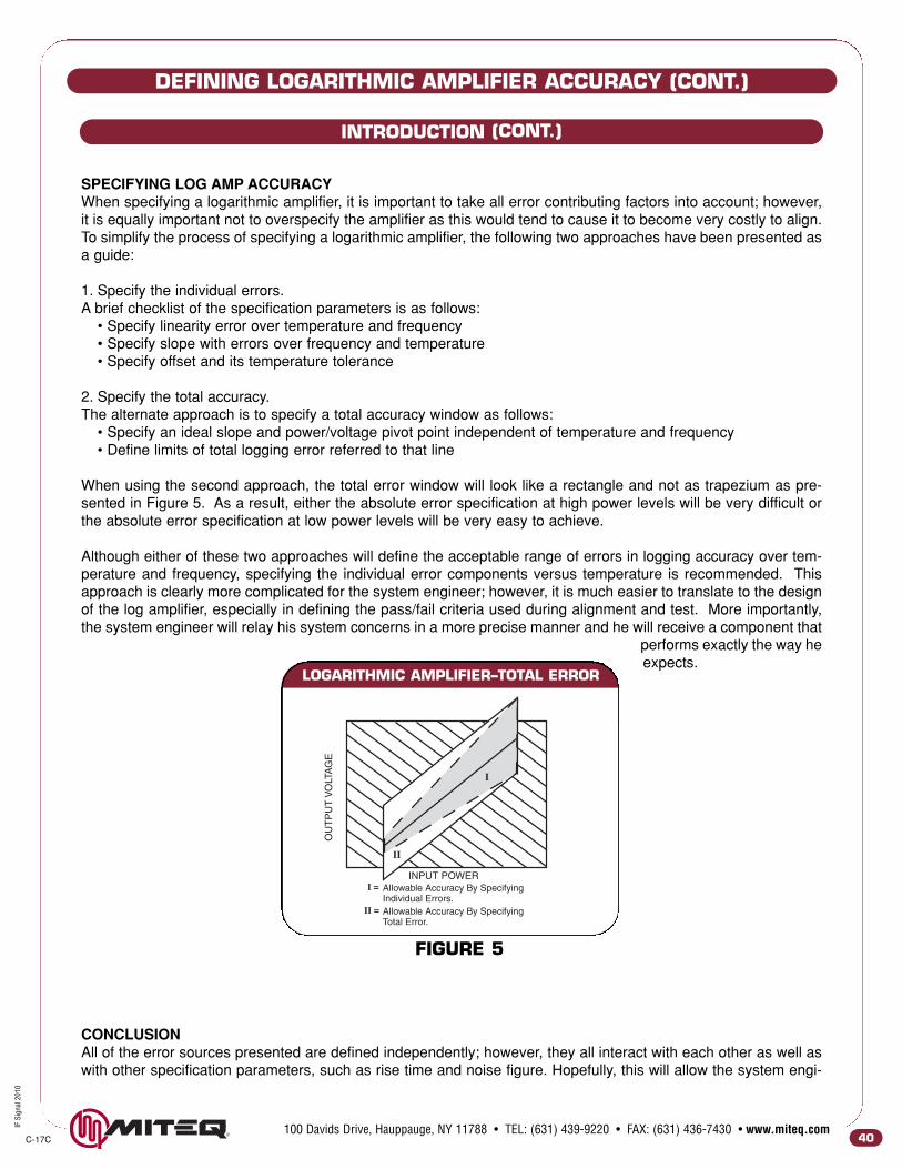
EFFECT OF THREE SOURCES OF ERROR ON OVERALL ACCURACYAll three sources of error will effect a logarithmic amplifier’s overall absolute accuracy. The definition of absoluteaccuracy is simply the difference between the measured output voltage to the ideal output voltage for a given inputpower. Each error will contribute differently over a set of conditions, such as temperature, frequency and powerlevel. The contributions of each error has been discussed with respect to temperature and frequency; however, itis easier to consider several of the errors when discussing their relation to input power.
At lower input signal levels, nearing TSS, the total errors are predominantly a result of the errors in offset and lin-earity; any errors due to slope inaccuracies are negligible. The slope variation versus temperature curve depictstypical logging curves over temperature extremes. From these curves it can be seen that the slope of a logarithmicamplifier tends to pivot about the minimum power point. At this pivot point the slope error is minimized and not afactor. At higher input power levels, the contribution of slope error must again be considered and factored into theoverall accuracy equation.
For clarification, the following is a list of the errors discussed with their relationship to temperature and frequency,as well as a look at how they can be combined to estimate the overall accuracy of a logarithmic amplifier:
TOTAL ERROR = Elinearity + Eoffset + Eslope
Linearity and slope errors are a function of both temperature and frequency, while offset is a function of frequencyalone. This total error can be depicted as in Figure 5. It defines the total range of output voltages that correspondto any input power range, and can be used in worst case system analysis.
FIGURE 4
SLOPE VARIATION VS. TEMPERATURE
39 C-17C100 Davids Drive, Hauppauge, NY 11788 • TEL: (631) 439-9220 • FAX: (631) 436-7430 • www.miteq.com IF
Signal2010
INTRODUCTION (CONT.)
OU
TP
UT
VO
LTA
GE
(V)
INPUT POWER (dBm)
-30°C
+25°C
+70°C
-80 -60 -40 -20 0
2
1.5
1
0.5
DEFINING LOGARITHMIC AMPLIFIER ACCURACY (CONT.)
SPECIFYING LOG AMP ACCURACYWhen specifying a logarithmic amplifier, it is important to take all error contributing factors into account; however,it is equally important not to overspecify the amplifier as this would tend to cause it to become very costly to align.To simplify the process of specifying a logarithmic amplifier, the following two approaches have been presented asa guide:
1. Specify the individual errors.A brief checklist of the specification parameters is as follows:• Specify linearity error over temperature and frequency• Specify slope with errors over frequency and temperature• Specify offset and its temperature tolerance
2. Specify the total accuracy.The alternate approach is to specify a total accuracy window as follows:• Specify an ideal slope and power/voltage pivot point independent of temperature and frequency• Define limits of total logging error referred to that line
When using the second approach, the total error window will look like a rectangle and not as trapezium as pre-sented in Figure 5. As a result, either the absolute error specification at high power levels will be very difficult orthe absolute error specification at low power levels will be very easy to achieve.
Although either of these two approaches will define the acceptable range of errors in logging accuracy over tem-perature and frequency, specifying the individual error components versus temperature is recommended. Thisapproach is clearly more complicated for the system engineer; however, it is much easier to translate to the designof the log amplifier, especially in defining the pass/fail criteria used during alignment and test. More importantly,the system engineer will relay his system concerns in a more precise manner and he will receive a component that
performs exactly the way heexpects.
CONCLUSIONAll of the error sources presented are defined independently; however, they all interact with each other as well aswith other specification parameters, such as rise time and noise figure. Hopefully, this will allow the system engi-
LOGARITHMIC AMPLIFIER–TOTAL ERROR
FIGURE 5
40C-17C100 Davids Drive, Hauppauge, NY 11788 • TEL: (631) 439-9220 • FAX: (631) 436-7430 • www.miteq.comIF
Signal2010
INTRODUCTION (CONT.)
OU
TP
UT
VO
LTA
GE
Allowable Accuracy By SpecifyingIndividual Errors.
INPUT POWERI =
Allowable Accuracy By Specifying Total Error.
II =
I
II
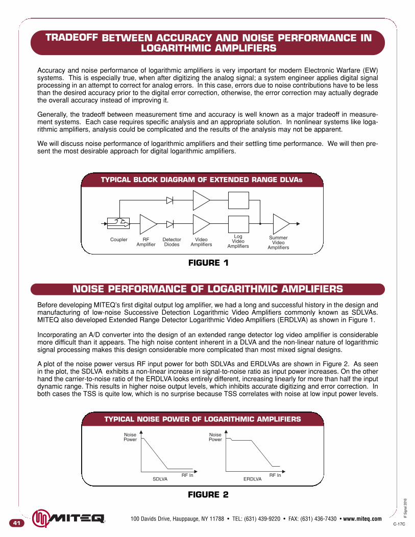
Accuracy and noise performance of logarithmic amplifiers is very important for modern Electronic Warfare (EW)systems. This is especially true, when after digitizing the analog signal; a system engineer applies digital signalprocessing in an attempt to correct for analog errors. In this case, errors due to noise contributions have to be lessthan the desired accuracy prior to the digital error correction, otherwise, the error correction may actually degradethe overall accuracy instead of improving it.
Generally, the tradeoff between measurement time and accuracy is well known as a major tradeoff in measure-ment systems. Each case requires specific analysis and an appropriate solution. In nonlinear systems like loga-rithmic amplifiers, analysis could be complicated and the results of the analysis may not be apparent.
We will discuss noise performance of logarithmic amplifiers and their settling time performance. We will then pre-sent the most desirable approach for digital logarithmic amplifiers.
TRADEOFF BETWEEN ACCURACY AND NOISE PERFORMANCE INLOGARITHMIC AMPLIFIERS
TYPICAL BLOCK DIAGRAM OF EXTENDED RANGE DLVAs
FIGURE 2
TYPICAL NOISE POWER OF LOGARITHMIC AMPLIFIERS
FIGURE 1
NOISE PERFORMANCE OF LOGARITHMIC AMPLIFIERS
Before developing MITEQ’s first digital output log amplifier, we had a long and successful history in the design andmanufacturing of low-noise Successive Detection Logarithmic Video Amplifiers commonly known as SDLVAs.MITEQ also developed Extended Range Detector Logarithmic Video Amplifiers (ERDLVA) as shown in Figure 1.
Incorporating an A/D converter into the design of an extended range detector log video amplifier is considerablemore difficult than it appears. The high noise content inherent in a DLVA and the non-linear nature of logarithmicsignal processing makes this design considerable more complicated than most mixed signal designs.
A plot of the noise power versus RF input power for both SDLVAs and ERDLVAs are shown in Figure 2. As seenin the plot, the SDLVA exhibits a non-linear increase in signal-to-noise ratio as input power increases. On the otherhand the carrier-to-noise ratio of the ERDLVA looks entirely different, increasing linearly for more than half the inputdynamic range. This results in higher noise output levels, which inhibits accurate digitizing and error correction. Inboth cases the TSS is quite low, which is no surprise because TSS correlates with noise at low input power levels.
41 C-17C100 Davids Drive, Hauppauge, NY 11788 • TEL: (631) 439-9220 • FAX: (631) 436-7430 • www.miteq.com IF
Signal2010
Coupler RFAmplifier
DetectorDiodes
VideoAmplifiers
LogVideo
Amplifiers
SummerVideo
Amplifiers
NoisePower
RF InSDLVA
NoisePower
RF InERDLVA

MAJOR SOURCE OF NOISE IN ERDLVAs
There are three major sources of noise that can effect a DLVAs performance. Two sources are the result of RFnoise downconversion. The third source is the video amplifier. To simplify our discussion we will define continu-ous white RF noise as in triple independent sources located equidistant within the frequency spectrum with 1 MHzspacing. This approximation is illustrated in Figure 3.
The definitions are as follows:
• Noise-Carrier Term-Noise Downconversion or N&CResulting from the RF noise downconversion due to beating between the RF carrierand the noise components.
• Noise-Noise Term-Noise Downconversion or N&NResulting from the RF noise downconversion due to beating between the differentnoise components.
• Video Amplifier Noise Contribution
FIGURE 3
NOISE SPECTRUM APPROXIMATION
42C-17C100 Davids Drive, Hauppauge, NY 11788 • TEL: (631) 439-9220 • FAX: (631) 436-7430 • www.miteq.comIF
Signal2010
1 MHzFcFc
PO
WE
R
FREQUENCYFREQUENCY
PO
WE
R

NOISE-CARRIER TERM-NOISE DOWNCONVERSION
Each arbitrarily taken noise component, with frequency Fi beats with carrier Fc and creates a baseband productwith a frequency of Fc - Fi. The resulting Root-Mean Square (RMS) voltage will be proportional to the RMS volt-ages of the carrier and the RF noise component. Therefore the RMS voltage of one beating pair (VoneBP) conver-sion is:
VoneBP = 2√2 (Kd/Rv) • Vc • VRFnoise (1)
The power of this baseband component expressed in mW:
PoneBP = 2(Kd2/Rv) • Pc • PRFnoise = 2M2 • Pc • PRFnoise (2)
Where:
Vc is the RMS voltage of the carrier
Pc is the power of the carrier expressed in mW
VRFnoise is the RMS voltage of the noise within a 1 MHz bandwidth
Kd is the detector’s sensitivity expressed in mV/mW
Rv is the detector’s video resistance in ohms
M is the detector’s figure of merit, which is equal to √(Kd2/Rv)
PRFnoise is noise power in mW within a 1 MHz bandwidth
Noise power in mW in a 1 MHz bandwidth itself depends on RF gain (GRF) and noise figure (NFRF).
PRFnoise = kT • 100.1(GRF + NFRF) (3)
Total noise power density (NPD in mW/MHz) in the baseband depends on the number of beating pairs (N)that will provide the equal baseband frequencies (Fc - Fi ).
NPD = PoneBP • N (4)
In the case of noise-carrier beating, N is frequency independent and equals two because the same product couldbe obtained from the carrier beating with two noise components, first with frequencies lower than the carrier andsecond with frequencies higher than the carrier.
Combining Equations (2) and (4) gives us:
NPD = 4M2 • PRFnoise • Pc(5)
The total noise power in mW of the noise-carrier term (PN&C) in the video bandwidth (BWvid) in MHz is equal to:
PN&C = NPD • BWvid = 4M2 • Pc • PRFnoise • BWvid(6)
PN&C does not depend on the RF bandwidth and is directly proportional to the following:
• The video bandwidth• The RF noise figure as part of Equation (3)• The input signal level
43 C-17C100 Davids Drive, Hauppauge, NY 11788 • TEL: (631) 439-9220 • FAX: (631) 436-7430 • www.miteq.com IF
Signal2010

NOISE-NOISE TERM-NOISE DOWNCONVERSION
Two arbitrarily taken noise components with frequencies Fi and Fj mix with each other to create two products, onewith the RF frequency Fi + Fj and the other with baseband frequency Fbb = Fi - Fj . For our discussion only thebaseband product is of interest.
Equation (2) is applicable to the noise-noise downconversion with the substitution of PC by another PRFnoise. So the power of the baseband product of the noise-noise beating pair is equal to:
PoneBP = 2M2 • P2RFnoise
(7)
Where:
PRFnoise is equal to the noise power in mW within a 1 MHz bandwidth, and expressed by Equation (3).
The number of beating pairs differs from the previous case significantly. In this case N depends on the frequencyof the baseband product Fbb where Fbb = Fi - Fj . It is apparent that each component gives a 1 MHz productwhen beating with adjacent components. Please refer to our approximation which assumes 1 MHz spacingbetween independent noise sources. So where Fbb = 1 MHz
For producing a 2 MHz product, each component has to mix with another one shifted by 2 MHz. In comparisonwith a 1 MHz product, we lose one beating pair.
And so on,
(8)
Combining Equations (4), (7) and (8) we get a baseband noise power density, NPD(Fbb), expressedin mW/MHz.
NPD(Fbb) = 2(Kd2/Rv) • P2
RFnoise • (BWRF - Fbb) (9)
N@Fbb = 2 MHz
BWRF
1 MHz- 1
N@Fbb = 3 MHz
BWRF
1 MHz- 2
N(Fbb)
N@Fbb = 1 MHz
BWRF
1 MHz
BWRF - Fbb
1 MHz
N@Fbb = 2 MHz
BWRF
1 MHz- 1
N@Fbb = 3 MHz
BWRF
1 MHz- 2
N(Fbb)
N@Fbb = 1 MHz
BWRF
1 MHz
BWRF - Fbb
1 MHz
N@Fbb = 2 MHz
BWRF
1 MHz- 1
N@Fbb = 3 MHz
BWRF
1 MHz- 2
N(Fbb)
N@Fbb = 1 MHz
BWRF
1 MHz
BWRF - Fbb
1 MHz
N@Fbb = 2 MHz
BWRF
1 MHz- 1
N@Fbb = 3 MHz
BWRF
1 MHz- 2
N(Fbb)
N@Fbb = 1 MHz
BWRF
1 MHz
BWRF - Fbb
1 MHz
44C-17C100 Davids Drive, Hauppauge, NY 11788 • TEL: (631) 439-9220 • FAX: (631) 436-7430 • www.miteq.comIF
Signal 2010

Therefore the total noise power in mW in the video bandwidth (BWvid in MHz) can be derived from the following:
PN&N = ∑ NPD (Fbb) = M2 (P2RFnoise • (2BWRF • BWvid - BW2
vid) = M2 • P2RFnoise • √BW2
eff (10)
Fbb
Where effective bandwidth BWeff is equal to:
BWeff = √2BWRF • BWvid - BW2vid (11)
PN&N is therefore directly proportional to the following:
• The video bandwidth• The RF noise figure as part of Equation (3)• The RF bandwidth
PN&N, on the other hand, does not depend on input signal level.
The noise power, expressed in mW, of the video amplifier into the video bandwidth is equal to:
PvidAmpNoise = 4kT • Fvid • BWvid (12)
Where the noise factor of the video amplifier (Fvid) is directly related to its noise figure as:
NFvid = 10log (Fvid) (13)
NOISE-NOISE TERM-NOISE DOWNCONVERSION (CONT.)
VIDEO AMPLIFIER NOISE CONTRIBUTION
45 C-17C 100 Davids Drive, Hauppauge, NY 11788 • TEL: (631) 439-9220 • FAX: (631) 436-7430 • www.miteq.com IF
Signal 2010

If the video bandwidth is less than the RF bandwidth, the noise-carrier term is independent of RF bandwidth. Thenoise-noise term is a function of video bandwidth. These differences become clear when we look at the NoisePower Density (NPD) of the terms.
Noise power density of the noise-carrier term is flat because the number of beating pairs equals two and is inde-pendent of the baseband product frequency. Extending the RF noise bandwidth does not increase the NPD,instead it stretches the baseband noise spectrum, as seen in Figure 4. Therefore the portion of the baseband noisespectrum, which remains after video filtering (shown by gray bar) does not depend on the RF bandwidth.
As seen in Figure 5, in the case of noise-noise downconversion, the number of beating pairs does depend on theRF bandwidth, as well as the frequency of the baseband product. Therefore the portion of the baseband noise spec-trum which remains after video filtering (shown by gray bar) increases proportionally with increasing RF bandwidth.
The difference between the N&N term and the N&C term is very important. It shows that by narrowing the RF band-width, one could improve TSS due to the reduction of the N&N term. At the same time it does not reduce noise atthe medium to high input power levels (almost the entire input dynamic range of the log amplifier), where the N&Cterm is dominant.
NOISE-CARRIER AND NOISE-NOISE TERMS AND THEIR DEPENDENCE ON BANDWIDTH
FIGURE 5
FIGURE 4
NOISE-CARRIER TERM
NOISE-NOISE TERM
46C-17C100 Davids Drive, Hauppauge, NY 11788 • TEL: (631) 439-9220 • FAX: (631) 436-7430 • www.miteq.comIF
Signal 2010
BWRF1
BWRF2
BWRF3
PO
WE
R
FREQUENCY
BWvid 0.5 x BWRF1
0.5 x BWRF2
0.5 x BWRF3
PO
WE
R
FREQUENCY
BWRF1
BWvidBW
RF1
PO
WE
R
PO
WE
R
FREQUENCY FREQUENCY
BWRF2
BWRF3
BWRF2
BWRF3

When we understand each noise source, obtain expressions of their noise power density [Equations (5) and (9)]and their noise power in the video bandwidth [Equations (6), (10) and (12)], we are able to compare the contribu-tion of these noise sources and understand which of the noise sources dominates under different conditions.
The N&C term is the only one which is directly proportional to the input power level of the carrier. This means thatat low input power levels, near TSS, the N&C term is insignificant. Therefore, at low power levels, only the N&N[Equation (10)] and the video amplifiers noise [Equation (12)] make significant contributions to the output noisepower.
Since N&C term is directly proportional to the input power, there must be a level (PCcr), where these terms haveequal contribution with the N&C term. Above PCcr, the N&C term will be dominant.
In comparing the three noise terms, the N&N terms contribution is very small (see NOTE 1) and may be disre-garded for practicality. Therefore, PCcr occurs when the N&C term [Equation (6)] is equal to the video amplifiersnoise term [Equation (12)] and can be calculated by the expression:
PCcr = 30 - 2GRF - NFRF + NFvid - 20logM (14)
Critical input power is an important parameter, because noise dependence versus input power level changes sig-nificantly around this point.
To calculate the noise power at the output of the log amplifier, one has to go through a few transformations. Weconvert the noise power at the detector’s output [Equations (6), (10) and (12)] into RMS voltages. We then multi-ply these voltages with the log video transfer function then transform back into power.
Upon completion we get the noise power of the log amplifier’s output, in dBm, for each noise term.
For the video amplifier’s noise term, which dominates when input power is less than the critical point:
PNoiseOut = -95 + 10log(Sl2/Rload) + 10logBWvid + NFvid - 20logM - 2GRF - 2PC (15)VidAmp
Where:
Sl is the slope of the DLVA in mV/dBRload is the video amplifier’s load resistor
The important feature of this equation is the rapid decline of noise power as a function of input power. This is dueto the term of -2PC.
For the N&C term, which dominates when input powers are above the critical point:
PNoiseOut = -125 + 10log(Sl2/Rload) + 10logBWvid + NFRF - PC (16)N&C
The important feature of this equation is a moderate decline of noise power as a function of input power. This isdue to the term of -1PC.
CONTRIBUTION OF DIFFERENT NOISE SOURCES
NOTE 1:This assumes that the RF system noise is insignificant. Usually the RF systems noise is greater than the video amplifier noise. Under this condition the N&C term and the N&N term will be most significant in the noise calculations.
47 C-17C 100 Davids Drive, Hauppauge, NY 11788 • TEL: (631) 439-9220 • FAX: (631) 436-7430 • www.miteq.com IF
Signal 2010

Plots of the output noise power versus input power for the ERDLVA with two detector stages are shown in Figures6A and 6B. Figure 6A presents the results taken on an ERDLVA with a center frequency of 500 MHz, with an inputdynamic range of -70 to 0 dBm. Figure 6B presents the results taken of an ERDLVA with a center frequency of 5.6GHz with an input dynamic range of -54 to +16 dBm.
Both examples demonstrate the measured output noise power correlate with results of our calculations. The impor-tant thing is, that for the high power stage, the noise versus input power degradation exhibits a constant slope of-2 while the low power stage changes its slope. It is -2 at low power levels and -1 at higher input power levels.When the input signal level is within the operating range of the low power stage, the noise from the high powerstage remains at the same high level and dominates over the noise of the low power stage.
Now that we understand all the sources of noise let us analyze the design of a low-noise DLVA.
One can see from Figure 6A and 6B that the high power stage makes a significant contribution in the total outputnoise magnitude even for input powers below this level. This being the case, to design a low-noise DLVA, we mustsuppress the noise from the high power stage over the input dynamic range of the low power stage. By doing thiswe only utilize the low noise portion of the high power stage.
Figure 7 presents the measured results of the DLVAs noise performance under the following conditions:
• The performance of a standard ERDLVA.• The noise performance of the low power stage when the high power stage is disconnected.• The noise performance of the low power stage shifted into the range of the high power stage while the high power stage is disconnected.
The noise reduction then becomes apparent. The only drawback of this approach is a substantial reduction in inputdynamic range of the analog output. However, we have developed a technique that would allow the restoration ofthe entire input dynamic range. This technique substantially improves processing speed and accuracy due to theaforementioned noise reduction.
We have applied this approach of noise reduction to an ERDLVA with a center frequency of 5.6 GHz and an inputdynamic range of -54 to +16 dBm. The results are shown in Figure 8. The first two plots in Figure 8 present the logaccuracy measured at the digital output over temperature, after digital error correction. The last graph presents theRMS error of the digital output, which is directly related to the noise of the analog portion. This RMS error was cal-culated on the basis of 400 samples for each 0.2 dB of input dynamic range. It becomes apparent from this plotthat logarithmic error reduces to less than ±0.25 dB and that three times the RMS error is less than ±0.2 dB.Successful usage of digital error correction is possible only due to the substantial suppression of the RMS noiselevel. A different approach to suppress the noise is using additional filtering. This can be done using either analogor digital techniques. However, additional filtering means narrower video bandwidth, which leads to increased set-tling time thereby increasing the minimum pulse width, which can be accurately measured.
MITEQ has overcome this limitation and offers an ERDLVA, which measures pulses as narrow as 250 ns, with anaccuracy of ±0.25 dB over 70 dB of input dynamic range.
RECONSTRUCTION OF THE NOISE POWER OUTPUTVERSUS INPUT POWER DEPENDENCE
LOW-NOISE ERDLVA DESIGN
48C-17C100 Davids Drive, Hauppauge, NY 11788 • TEL: (631) 439-9220 • FAX: (631) 436-7430 • www.miteq.comIF
Signal 2010

FIGURE 6A
OUTPUT NOISE POWER OF A 500 MHz ERDLVA
FIGURE 6B
OUTPUT NOISE POWER OF A 5.6 GHz ERDLVA
LOW-NOISE ERDLVA DESIGN TYPICAL TEST DATA
49 C-17C 100 Davids Drive, Hauppauge, NY 11788 • TEL: (631) 439-9220 • FAX: (631) 436-7430 • www.miteq.com IF
Signal 2010
0
-10
-20
-30
-40
-50
-60-70 -30-60 -50
INPUT POWER (dBm)
OU
TP
UT
NO
ISE
PO
WE
R (
dBm
)
High Power StageLow Power StageBoth Stages
-20 -10 0-40
-15
-20
-25
-30
-35
-40
-45-70-80 -30-60 -50
INPUT POWER (dBm)
OU
TP
UT
NO
ISE
PO
WE
R (
dBm
)
-20 -10 0-40
High Power StageLow Power StageBoth Stages
0
-10
-20
-30
-40
-50
-60-70 -30-60 -50
INPUT POWER (dBm)
OU
TP
UT
NO
ISE
PO
WE
R (
dBm
)
High Power StageLow Power StageBoth Stages
-20 -10 0-40
-15
-20
-25
-30
-35
-40
-45-70-80 -30-60 -50
INPUT POWER (dBm)
OU
TP
UT
NO
ISE
PO
WE
R (
dBm
)
-20 -10 0-40
High Power StageLow Power StageBoth Stages

High Power StageLow Power StageBoth Stages
High Power StageLow Power StageBoth Stages
High Power StageLow Power Stage
High Power Stage
Low Power Stage
High Power StageLow Power StageBoth Stages
STANDARD DLVA
NO
ISE
VO
LTA
GE
(m
V/R
MS
)
100
10
1-80 -70 -60 -50 -40
INPUT POWER (dBm)
INPUT POWER (dBm)
INPUT POWER (dBm) INPUT POWER (dBm)
INPUT POWER (dBm)
INPUT POWER (dBm)
LOW POWER STAGE W/O HIGH POWER STAGE (dBm)
LOW POWER STAGE SHIFTED INTO HIGH POWER RANGE (dBm) LOW POWER STAGE SHIFTED INTO HIGH POWER RANGE (dBm)
LOW POWER STAGE W/O HIGH POWER STAGE (dBm)
-30 -20 -10 0
NO
ISE
VO
LTA
GE
(m
V/R
MS
)
100
10
1-80 -70 -60 -50 -40 -30 -20 -10 0
NO
ISE
VO
LTA
GE
(m
V/R
MS
)
100
10
1-80 -70 -60 -50 -40 -30 -20 -10 0
OU
TP
UT
VO
LTA
GE
(m
V)
-80 -70 -60 -50 -40 -30 -20 -10 0
-80 -70 -60 -50 -40 -30 -20 -10 0
STANDARD DLVA
OU
TP
UT
VO
LTA
GE
(m
V)
OU
TP
UT
VO
LTA
GE
(m
V)
3000
2500
2000
1500
1000
500
0
3000
2500
2000
1500
1000
500
0
3000
2500
2000
1500
1000
500
0
-80 -70 -60 -50 -40 -30 -20 -10 0
High Power StageLow Power Stage
FIGURE 7
LOW-NOISE ERDLVA DESIGN TYPICAL TEST DATA (CONT.)
50C-17C100 Davids Drive, Hauppauge, NY 11788 • TEL: (631) 439-9220 • FAX: (631) 436-7430 • www.miteq.comIF
Signal 2010

DIGITAL ERDLVA DESIGN TYPICAL TEST DATA
LIN
EA
RIT
Y (
dB)
1
0.5
0
-0.5
-1-60 -50 -40 -30 -10-20 0 10 20
Temperature @ 20°CAbsolute Accuracy, dB
PIN (dBm)
LIN
EA
RIT
Y (
dB)
1
0.5
0
-0.5
-1-60 -50 -40 -30 -10-20 0 10 20
Temperature @ 40°CAbsolute Accuracy, dB
PIN (dBm)
1024
768
512
256
0
1
0
-1/1
-60 -50 -40 -30 -10-20 0 10 20
Temperature Reading @ 40°CDigital Reading
4 Sigma, Min., Max.
MODEL NO. FBDL-5.4/5.9-70SERIAL NO. 489150
PIN (dBm)
-60 -50 -40 -30 -10-20 0 10 20
PIN (dBm)
DIG
ITA
L O
UT
PU
TE
RR
OR
DIS
TR
IBU
TIO
N
FIGURE 8
51 C-17C 100 Davids Drive, Hauppauge, NY 11788 • TEL: (631) 439-9220 • FAX: (631) 436-7430 • www.miteq.com IF
Signal 2010


MITEQ TO RHG IF PRODUCTS CROSS REFERENCE GUIDE
LOGARITHMIC AMPLIFIERSRHG MODEL MITEQ MODEL
ICLW1000 MLIFQ-1000500-60BICLWP300 MLIFQ-300400-60KICLWP400 MLIFQ-400400-60KICLWP750 MLIFQ-750500-60KICLWP1000 MLIFQ-1000500-60KICLWX450 MLIFQ-450500F-60BICLWX750 MLIFQ-750500F-60BICLWX1000 MLIFQ-1000500F-60BICLX1002 LIFDQ-1002P-80BICLX2005 LIFDQ-2005P-80BICLX2105 LIFDQ-2105P-80BICLX3010 LIFDQ-3010P-80BICLX6010 LIFDQ-6010P-80BICLX6020 LIFD-6020P-80BICLX7010 LIFDQ-7010P-80BICLX7030 LIFDQ-7030P-80BICLX12020 LIFDQ-12020P-70BICLX16020 LIFDQ-16020P-70BICLX16040 LIFDQ-16040P-70B ICLX200 LIFDQ-20050P-70BILM3010 LIFDQ-3010-80FILM6020 LIFDQ-6020-80FILM7030 LIFDQ-7030-80FILM12020 LIFDQ-12020-70FILM16040 LIFDQ-16040-70F ILM200 LIFDQ-20050-70FLLT1003 LIFDQ-1003-80HLLT2005 LIFDQ-2005-80HLLT3002 LIFDQ-3002-80HLLT3010 LIFDQ-3010-80HLLT6010 LIFDQ-6010-80H LLT6020 LIFDQ-6020-80HLLT7010 LIFDQ-7010-80HLST1003 LIFDQ-1003-80ILST2005 LIFDQ-2005-80ILST3002 LIFDQ-3002-80ILST3010 LIFDQ-3010-80ILST6010 LIFDQ-6010-80ILST6020 LIFDQ-6020-80ILST7010 LIFDQ-7010-80IML2105 LIFDQ-2105-70CML3010 LIFDQ-3010-70CML6010 LIFDQ-6010-70CML6020 LIFDQ-6020-70CML7010 LIFDQ-7010-70CML12020 LIFDQ-12020-60CML16040 LIFDQ-16040-60C
RHG MODEL MITEQ MODEL
ICLL2105 LIFDQ-2105-80DICLL3010 LIFDQ-3010-80DICLL6010 LIFDQ-6010-80DICLL6020 LIFDQ-6020-80DICLL7030 LIFDQ-7030-80DICLL12020 LIFDQ-12020-70DICLL150 LIFDQ-150100-70DICLL16040 LIFDQ-16040-70DICLL200 LIFDQ-20050-70DICLLW300 MLIFQ-300/400-60DICLLW400 MLIFQ-400/400-60DICLLW750 MLIFQ-750/500-60DCICLP1002 LIFDQ-1002-80KICLP2005 LIFDQ-2005-80KICLP2105 LIFDQ-2105-80KICLP3010 LIFDQ-3010-80KICLP6010 LIFDQ-6010-80KICLP6020 LIFDQ-6020-80KICLP7010 LIFDQ-7010-80KICLP12020 LIFDQ-12020-70KICLP16020 LIFDQ-16020-70KICLP16040 LIFDQ-16040-70KICLP20050 LIFDQ-20050-70KICLT1002 LIFDQ-1002-80BICLT2005 LIFDQ-2005-80BICLT2105 LIFDQ-2105-80BICLT3010 LIFDQ-3010-80BICLT6010 LIFDQ-6010-80BICLT6020 LIFDQ-6020-80BICLT7010 LIFDQ-7010-80BICLT7030 LIFDQ-7030-80BICLT12020 LIFDQ-12020-70BICLT16020 LIFDQ-16020-70BICLT16040 LIFDQ-16040-70BICLT150B LIFDQ-150100-70GLICLT200 LIFDQ-20050-70BICLT300B LIFDQ-300200-60GLICLT375B LIFDQ-375250-60GLICLT450B MLIFQ-450300-60GLICLT475BC MLIFQ-475150-60GLICLT625B MLIFQ-625150-60GLICLT775B MLIFQ-775150-60GLICLT925B MLIFQ-925150-60GLICLT1000B MLIFQ-1000100-60GLICLW300 MLIFQ-300400-65BICLW400 MLIFQ-400400-60BICLW750 MLIFQ-750500-60B
INTRODUCTIONThe MITEQ models noted herein are designed to be form-fit replacements of the referenced RHG counterparts.They are equivalent in all RF and video characteristics; however, there may be some differences in the technolo-gies used to manufacture the MITEQ models, resulting in slight changes in parameters such as DC power con-sumption, thermal dissipation and weight. In addition, you may observe subtle improvements in operating charac-teristics such as bandwidth, 1 dB compression point and pulse rise time. You should be assured that the MITEQunits shall meet or exceed the RHG specified performance.
53 C-17C 100 Davids Drive, Hauppauge, NY 11788 • TEL: (631) 439-9220 • FAX: (631) 436-7430 • www.miteq.com IF
Signal 2010

FREQUENCY DISCRIMINATORS
LIMITING AMPLIFIERS
RHG MODEL MITEQ MODEL
DT1004 FMDMQ-10/4-250I
DT2004 FMDMQ-20/4-250I
DT3006 FMDMQ-30/6-200I
DT6006 FMDMQ-60/6-200I
DT6016 FMDMQ-60/16-100I
DT7020 FMDMQ-70/20-70I
DT13035 FMDMQ-130/35-30I
DT16035 FMDMQ-160/35-30I
ICDL3006 FMDMQ-30/6-200G
ICDL6016 FMDMQ-60/16-100G
ICDL7020 FMDMQ-70/20-70G
ICDL16035 FMDMQ-160/35-15G
ICDL300 FMDMQ-300/70-20G
ICDL400 FMDMQ-400/70-20G
ICDL750 FMDMQ-750/150-20G
ICDLP3006 FMDMQ-30/6-200E
ICDLP6016 FMDMQ-60/16-100E
ICDLP7020 FMDMQ-70/20-70E
ICDLP16035 FMDMQ-160/35-15E
ICDLP300 FMDMQ-300/70-20E
RHG MODEL MITEQ MODEL
ICDLP400 FMDMQ-400/70-20E
ICDLP750 FMDMQ-750/150-20E
ICDS750 FMDMQ-750/250-5B
ICDS1000 FMDMQ-1000/300-5B
ICDT2104 FMDMQ-21/4-250B
ICDT3006 FMDMQ-30/6-200B
ICDT6016 FMDMQ-60/16-100B
ICDT7020 FMDMQ-70/20-70B
ICDT16035 FMDMQ-160/35-30B
ICDT300 FMDMQ-300/70-20B
ICDT450 FMDMQ-450/70-20B
ICDT750 FMDMQ-750/150-20B
ICDX30 FMDMQ-30/10-150A
ICDX60 FMDMQ-60/15-70A
ICDX70 FMDMQ-70/17-70A
ICDX160 FMDMQ-160/50-30A
ICDX300 FMDMQ-300/60-20A
ICDX400 FMDMQ-400/90-20A
ICDX750 FMDMQ-750/250-20A
ICDX1000 FMDMQ-1000/300-20A
RHG MODEL MITEQ MODEL
ICUL400 LCPMQ-400/100-55G
ICULM2105 LCPMQ-21/5-65GM-
ICULM3010 LCPMQ-30/10-65GM-
ICULM6020 LCPMQ-60/20-65GM-
ICULM7010 LCPMQ-70/10-65GM-
ICULM12020 LCPMQ-120/20-65GM-
ICULM16020 LCPMQ-160/20-65GM-
ICULM16040 LCPMQ-160/40-65GM-
ICULM200 LCPMQ-200/50-55GM-
ICULM300 LCPMQ-300/75-55GM-
ICULM400 LCPMQ-400/100-55GM-
ISM3010 LCPMQ-30/10-65D
ISM6010 LCPMQ-60/10-65D
ISM6020 LCPMQ-60/20-65D
ISM7010 LCPMQ-70/10-65D
ISM16020 LCPMQ-160/20-65D
ISM16040 LCPMQ-160/40-65D
ISMP3010 LCPMQ-30/10-65E
ISMP6010 LCPMQ-60/10-65E
ISMP6020 LCPMQ-60/20-65E
ISMP7010 LCPMQ-70/10-65E
ISMP16020 LCPMQ-160/20-65E
ISMP16040 LCPMQ-160/40-65E
RHG MODEL MITEQ MODEL
ICSH2105 LCPMQ-21/5-80B
ICSH3010 LCPMQ-30/10-80B
ICSH6020 LCPMQ-60/20-80B
ICSH7010 LCPMQ-70/10-80B
ICSH12020 LCPMQ-120/20-80B
ICSH16020 LCPMQ-160/20-70B
ICSH16040 LCPMQ-160/40-70B
ICSHM2105 LCPMQ-21/5-80BM-
ICSHM3010 LCPMQ-30/10-80BM-
ICSHM6020 LCPMQ-60/20-80BM-
ICSHM7010 LCPMQ-70/10-80BM-
ICSHM12020 LCPMQ-120/20-80BM-
ICSHM16020 LCPMQ-160/20-70BM-
ICSHM16040 LCPMQ-160/40-70BM-
ICUL2105 LCPMQ-21/5-65G
ICUL3010 LCPMQ-30/10-65G
ICUL6020 LCPMQ-60/20-65G
ICUL7010 LCPMQ-70/10-65G
ICUL12020 LCPMQ-120/20-65G
ICUL16020 LCPMQ-160/20-65G
ICUL16040 LCPMQ-160/40-65G
ICUL200 LCPMQ-200/50-55G
ICUL300 LCPMQ-300/75-55G
MITEQ TO RHG IF PRODUCTS CROSS REFERENCE GUIDE (CONT.)
54C-17C100 Davids Drive, Hauppauge, NY 11788 • TEL: (631) 439-9220 • FAX: (631) 436-7430 • www.miteq.comIF
Signal 2010

MITEQ TO RHG IF PRODUCTS CROSS REFERENCE GUIDE (CONT.)
GAIN-CONTROL AMPLIFIERSRHG MODEL MITEQ MODEL
AGC/10 DRV/10AGC/11 SP-2-30160GCAGC-12C SP-3-30/10GCAGC-12B SP-3-60/20GCAGC-12EF SP-3-160/40GCEST3002 AGCQ-8PDV-30/2EEST3010 AGCQ-8PDV-30/10EEST6010 AGCQ-8PDV-60/10EEST6020 AGCQ-8PDV-60/20EEST7030 AGCQ-6PDV-70/30EEST12020 AGCQ-6PDV-120/20EEST16040 AGCQ-6PDV-160/40EET1002 VGCQ-8-10/2EET2004 VGCQ-8-20/4EET3002 VGCQ-8-30/2EET3010 VGCQ-8-30/10EET6010 VGCQ-8-60/10EET6020 VGCQ-8-60/20EET7010 VGCQ-8-70/10EET7030 VGCQ-6-70/30EET12020 VGCQ-6-120/20EET16040 VGCQ-6-160/40EEVT1002 VGCQ-8DV-10/2EEVT2004 VGCQ-8DV-20/4EEVT3002 VGCQ-8DV-30/2EEVT3010 VGCQ-8DV-30/10EEVT6010 VGCQ-8DV-60/10EEVT6020 VGCQ-8DV-60/20EEVT7010 VGCQ-8DV-70/10EEVT7030 VGCQ-6DV-70/30EEVT12020 VGCQ-6DV-120/20EEVT16040 VGCQ-6DV-160/40EICE2004 VGCQ-7-20/4BICE2104 VGCQ-7-21/4BICE3010 VGCQ-7-30/10BICE6010 VGCQ-7-60/10BICE6020 VGCQ-7-60/20BICE7010 VGCQ-7-70/10BICE7030 VGCQ-7-70/30BICE12040 VGCQ-6-120/40BICE16040 VGCQ-6-160/40BICEGT2104 VGCQ-7PDV-21/4DICEGT3004 VGCQ-7PDV-30/4DICEGT3010 VGCQ-7PDV-30/10DICEGT6010 VGCQ-7PDV-60/10DICEGT6020 VGCQ-7PDV-60/20DICEGT7020 VGCQ-7PDV-70/20DICEGT12040 VGCQ-6PDV-120/40DICEGT16040 VGCQ-6PDV-160/40DICEMT2104 VGCQ-7PDV-21/4DM-ICEMT3004 VGCQ-7PDV-30/4DM-ICEMT3010 VGCQ-7PDV-30/10DM-ICEMT6010 VGCQ-7PDV-60/10DM-ICEMT6020 VGCQ-7PDV-60/20DM-
RHG MODEL MITEQ MODEL
ICEMT7020 VGCQ-7PDV-70/20DM-ICEMT12040 VGCQ-6PDV-120/40DM-ICEMT16040 VGCQ-6PDV-160/40DM-ICEST2104 AGCQ-7PDV-21/4DICEST3004 AGCQ-7PDV-30/4DICEST3010 AGCQ-7PDV-30/10DICEST6010 AGCQ-7PDV-60/10DICEST7020 AGCQ-7PDV-70/20DICEST12040 AGCQ-6PDV-120/40DICEST16040 AGCQ-6PDV-160/40DICEVT2004 VGCQ-7DV-20/4BICEVT2104 VGCQ-7DV-21/4BICEVT3010 VGCQ-7DV-30/10BICEVT6010 VGCQ-7DV-60/10BICEVT6020 VGCQ-7DV-60/20BICEVT7010 VGCQ-7DV-70/10BICEVT7030 VGCQ-7DV-70/30B ICEVT12040 VGCQ-6DV-120/40BICEVT16040 VGCQ-7DV-160/40BICFG3010 SPGQ-30/10-20ICFH2006 SPHQ-20/6-15ICFH2106 SPHQ-21/6-15ICFH3010 SPHQ-30/10-15ICFH6010 SPHQ-60/10-15ICFH6020 SPHQ-60/20-15ICFH6040 SPHQ-60/40-15ICFH7030 SPHQ-70/30-15ICFH120LN SPHQ-120/40-13ICFH160LN SPHQ-160/50-13ICFL3010 SPLQ-30/10-0LNICFT2006 SPTQ-20/6ICFT2106 SPTQ-21/6ICFT3010 SPTQ-30/10ICFT6010 SPTQ-60/10ICFT6020 SPTQ-60/20ICFT6040 SPTQ-60/40ICFT7030 SPTQ-70/30ICFT12040 SPTQ-120/40ICFT16050 SPTQ-160/50ICFT300 SPTQ-145/290CFV2006 VGCQ-2SP-20/6FICFV2106 VGCQ-2SP-21/6FICFV3010 VGCQ-2SP-30/10FICFV6010 VGCQ-2SP-60/10FICFV6020 VGCQ-2SP-60/20FICFV6040 VGCQ-2SP-60/40FICFV7030 VGCQ-2SP-70/30FICFV12040 VGCQ-2SP-120/40FICFV16060 VGCQ-2SP-160/60FICXT2205 AGCQ-7PDV-22/5SPICXT3005 AGCQ-7PDV-30/5SPICXT3010 AGCQ-7PDV-30/10SPICXT6010 AGCQ-7PDV-60/10SPICXT6020 AGCQ-7PDV-60/20SP
55 C-17C 100 Davids Drive, Hauppauge, NY 11788 • TEL: (631) 439-9220 • FAX: (631) 436-7430 • www.miteq.com IF
Signal 2010

MITEQ TO RHG IF PRODUCTS CROSS REFERENCE GUIDE (CONT.)
CUSTOM MODELS
ORDERING INFORMATION• Standard models available with +12 volt power supply
• For +15 volt power supply option, add suffix “C” (no charge)
• Standard operating temperature range is -40 to +70°C, optional temperature ranges are available, contact MITEQ
• For outline drawings, contact MITEQ
AVAILABLE OPTIONS• Customized center frequencies• Alternate operational bandwidth• Customized dynamic ranges• Gain and phase tracking/matching• Hermetically-sealed units• Military screening• Temperature compensation• Fast rise times• Custom-integrated multifunction units
RHG MODEL MITEQ MODEL
EST40A22DB AGC-6PDV-40/10E
EST60V41 VGCQ-8PDV-60/10TR
EST4004 AGCQ-7P-40/4ECTNC
EVT35F89 AGCQ-7DV-35/3.4SP
EVT35CC17A AGCQ-7DV-35/10SP
ICE30C17BH VGCQ-7P-30/12GM
ICE10.7D04RV VGCQ-7PDV-10.7/1D
ICE160J05DA VGCQ-6PDV-160/40B
ICE30BH27 VGC-7P-30/10BC
ICE160J26NA VGC-6PDV-160/50BC
ICE160J25NB VGCQ-6DV-160/100BC
ICF10.7D04RV VGC-2-10/1F
ICD160G20BL FMDMQ-160/35-15B
ICD160F22GB FMDMQ-160/50-25AC
RHG MODEL MITEQ MODEL
ICD160F22GA FMDMQ-160/5-15BC
ICL145A20RA LIFDQ-14510-80B
ICL30M15MB LIFDQ-3010P-80KCL
ICL160J25NA LIFDQ-160100-80BCL
ICL21J21LA LIFDQ-2110-80BL
ICLT160G20BK LIFDQ-16040-70BL
ICL5G10CH LIFDQ-5/0.8-90
ICL145B28JA LIFDQ-14510-080B
ICL21F18CH LIFDQ-21.4/10-70
LST30D09EA LIFD-30/10-080ICL
ILM160C02NA LIFDQ-16040P-070FC
LLT6020/MOD LIFDQ-6020S-80H
ICS160F09GB LCPMQ-160/50-65BC
56C-17C100 Davids Drive, Hauppauge, NY 11788 • TEL: (631) 439-9220 • FAX: (631) 436-7430 • www.miteq.comIF
Signal 2010

This page is intentionally blank

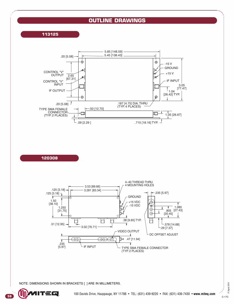
OUTLINE DRAWINGS
59 C-17C100 Davids Drive, Hauppauge, NY 11788 • TEL: (631) 439-9220 • FAX: (631) 436-7430 • www.miteq.com IF
Signal2010NOTE: DIMENSIONS SHOWN IN BRACKETS [ ] ARE IN MILLIMETERS.
-15 V
CONTROL "V"OUTPUT
CONTROL "V"INPUT
.715 [18.16] TYP.
GROUND
+15 V
IF INPUT
IF OUTPUT
1.05 [26.67]
TYPE SMA FEMALECONNECTOR
(TYP. 2 PLACES)
.187 [4.75] DIA. THRU(TYP. 4 PLACES)
1.04[26.42] TYP.
3.05[77.47]
.20 [5.08]
2.65[67.31]
.50 [12.70]
5.85 [148.59]5.45 [138.43].20 [5.08]
.09 [2.29 ]
113125
120308
IF INPUT TYPE SMA FEMALE CONNECTOR(TYP. 2 PLACES)
VIDEO OUTPUT
-15 VDC+15 VDC
GROUND
4–40 THREAD THRU4 MOUNTING HOLES
DC OFFSET ADJUST
.51 [12.95]3.02 [76.71]
.125 [3.18]
1.250[31.75]
1.50[38.10]
.125 [3.18] 3.281 [83.34]3.53 [89.66]
.235[5.97]
.47 [11.94]
.29 [7.37].578 [14.68]
.805[20.45]
1.080[27.43]
.235 [5.97]
.38 [9.65] TYP.

OUTLINE DRAWINGS (CONT.)
60C-17C100 Davids Drive, Hauppauge, NY 11788 • TEL: (631) 439-9220 • FAX: (631) 436-7430 • www.miteq.comIF
Signal2010 NOTE: DIMENSIONS SHOWN IN BRACKETS [ ] ARE IN MILLIMETERS.
IF INPUT SMA FEMALE
GAINCONTROL
+15 VDC-15 VDC
IF OUTPUT SMA FEMALE
I
GROUND1.08
[27.43].805
[20.45]
.578[14.68]
.29[7.37]
IF GAIN
VIDEO OUTPUTSMA FEMALE
4–40 THREAD THRU4 MOUNTING HOLES
.235 [5.97]DC OFFSET
ADJUST
4.62 [117.35]4.38 [111.25]
2.88 [73.15]
1.83 [46.48]
4.17 [105.92]
2.53 [64.26].45 [11.43]
.235 [5.97]
.125 [3.18].125 [3.18]
1.25[31.75]
1.50[38.10]
.47 [11.94]
.32 [8.13] TYP.
120338
120309
IF INPUT TYPE SMA FEMALE CONNECTOR(TYP. 2 PLACES)
VIDEO OUTPUT
-15 VDC+15 VDC
GROUND
4–40 THREAD THRU4 MOUNTING HOLES
DC OFFSET ADJUST
.51 [12.95]3.02 [76.71]
.125 [3.18]
1.250[31.75]
1.50[38.10]
.125 [3.18] 3.281 [83.34]3.53 [89.66]
.235[5.97]
.47 [11.94]
.29 [7.37].578 [14.68]
.805[20.45]
1.080[27.43]
.235 [5.97]
.38 [9.65] TYP.

OUTLINE DRAWINGS (CONT.)
61 C-17C100 Davids Drive, Hauppauge, NY 11788 • TEL: (631) 439-9220 • FAX: (631) 436-7430 • www.miteq.com IF
Signal2010NOTE: DIMENSIONS SHOWN IN BRACKETS [ ] ARE IN MILLIMETERS.
IF INPUT
GROUND
-15 VDC
VIDEO OUTPUT
SMA FEMALE CONNECTOR(2 PLACES)
4–40 THREAD THRU4 MOUNTING HOLES
.51[12.95]
.235[5.97]
1.25[31.75]
1.50[38.10]
.125 [3.18].125 [3.18] .235 [5.97]
.38 [9.65] TYP.
.47 [11.94]
.805 [20.45]
.290 [7.37]3.02
[76.71]
3.281 [83.34]3.53 [89.66]
120392
120391
IF INPUT
GROUND
+15 VDC-15 VDC
IFOUTPUT
GROUND1.08
[27.43].805
[20.45]
.578[14.68]
.29[7.37]
GAIN CONTROL
VIDEOOUTPUT
4–40 THREAD THRU4 MOUNTING HOLES
.235 [5.97]DC OFFSET
ADJUST
3.53 [89.66]3.281 [83.34]
1.50 [38.10]2.33 [59.18]3.02 [76.71]
1.25 [31.75].51 [12.95]
.235 [5.97]
.125 [3.18].125 [3.18]
1.25[31.75]
1.50[38.10]
.47 [11.94]
.38 [9.65] TYP.
TYPE SMA FEMALECONNECTORS(3 PLACES)

OUTLINE DRAWINGS (CONT.)
62C-17C100 Davids Drive, Hauppauge, NY 11788 • TEL: (631) 439-9220 • FAX: (631) 436-7430 • www.miteq.comIF
Signal2010 NOTE: DIMENSIONS SHOWN IN BRACKETS [ ] ARE IN MILLIMETERS.
3.25 [82.55]2.50 [63.50]
.531 [13.49]
.235 [5.97]
1.25[31.75]
1.50[38.10]
.125 [3.18].125 [3.18]
4–40 THREAD THRU4 MOUNTING HOLES3.531 [89.69]
3.78 [96.01]
.235 [5.97]GROUND
+VDC-VDC
.38 [9.65] TYP.
.47 [11.94]
VIDEO OUTPUTLIMITED IFOUTPUT
TYPE SMA FEMALECONNECTORS(3 PLACES)
IF INPUT
.29 [7.37].578 [14.68]
.805[20.45]
1.08[27.43]
DC OFFSETADJUST
120721
2.00[50.80]
4.00 [101.60]GROUND
+VDC-VDC
RFOUTPUT
1.00 [25.40]
RF INPUT .38 [9.65] TYP.
.3750 [9.53]
.35 [8.89]
.13 [3.30]4–40 MOUNTING HOLES(2 PLACES)
.28 [7.11]
.60 [15.24]
1.20[30.48]
1.50[38.10]
TYPE SMA FEMALECONNECTIONBOTH ENDS
1.80[45.72]
.35 [8.89].60 [15.24]
120935

OUTLINE DRAWINGS (CONT.)
63 C-17C100 Davids Drive, Hauppauge, NY 11788 • TEL: (631) 439-9220 • FAX: (631) 436-7430 • www.miteq.com IF
Signal2010NOTE: DIMENSIONS SHOWN IN BRACKETS [ ] ARE IN MILLIMETERS.
IF INPUT.235[5.97]
.47 [11.94]
.125 [3.18].125 [3.18]
1.25[31.75]
1.50[38.10]
GROUND-15 VDC
2.250 [57.15]
2.50 [63.50]
2.03 [51.56].47 [11.94]
.32 [8.13]
.235 [5.97]
IF OUTPUT
TYPE SMA FEMALE CONNECTOR(2 PLACES)
.578 [14.68]
.805 [20.45]
4–40 THREAD THRUW/.156 [3.96] DIA. X .062 [1.57] DEEPC'BORE EACH SIDE(4 MOUNTING HOLES)
121954
1.50[38.10]
1.25[31.75]
.453[11.51]
.234 [5.94]
SMA FEMALECONNECTOR(TYP. 3 PLACES)
CONNECTORCANNONMDM9SH003PMATE & CABLESUPPLIED
.140 [3.56] DIA.MOUNTING HOLES(TYP. 4 PLACES)
IFIN
LIMITEDIF
OUTVIDEOOUT OFFSET
PWR
4.375 [111.13]4.125 [104.78]
3.578 [90.88]3.031 [76.99]
2.375 [60.33]
.125 [3.18].125 [3.18]
121831
* ABOVE DRAWING INCLUDES LIMITED IF OUTPUT (OPTIONAL).
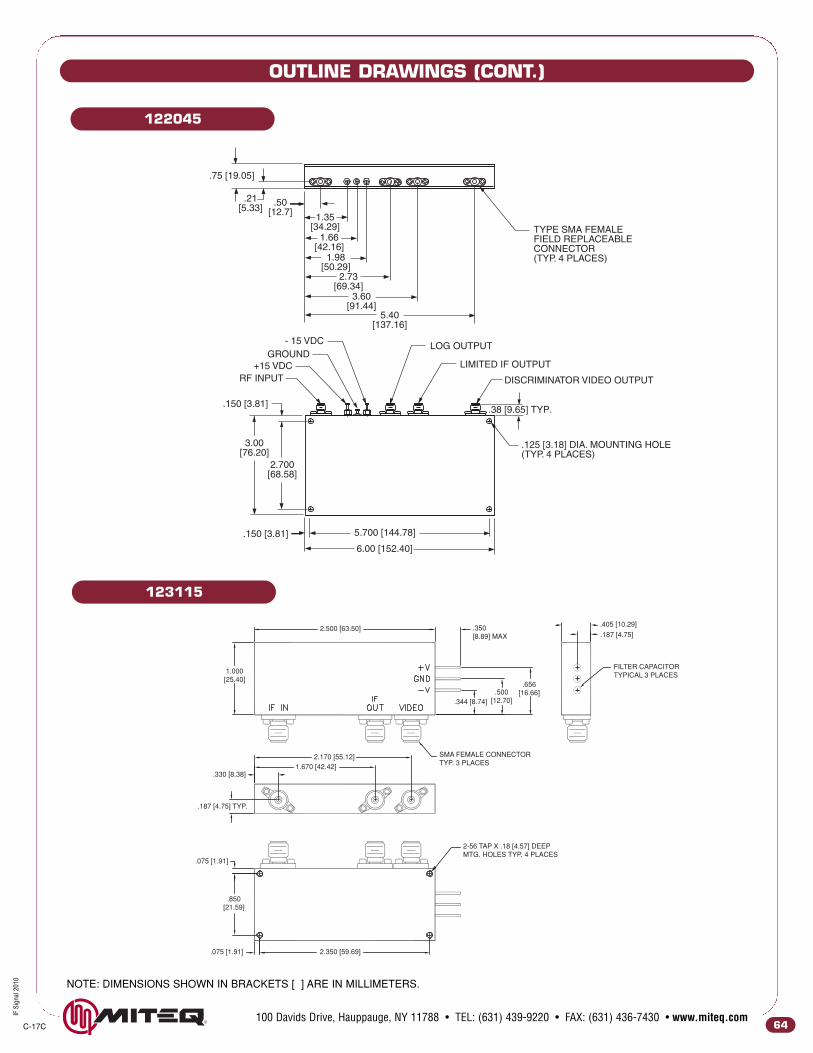
OUTLINE DRAWINGS (CONT.)
64C-17C100 Davids Drive, Hauppauge, NY 11788 • TEL: (631) 439-9220 • FAX: (631) 436-7430 • www.miteq.comIF
Signal2010 NOTE: DIMENSIONS SHOWN IN BRACKETS [ ] ARE IN MILLIMETERS.
5.700 [144.78].150 [3.81]
.150 [3.81]
RF INPUT
LOG OUTPUT
DISCRIMINATOR VIDEO OUTPUT
.38 [9.65] TYP.
.125 [3.18] DIA. MOUNTING HOLE(TYP. 4 PLACES)
TYPE SMA FEMALEFIELD REPLACEABLECONNECTOR(TYP. 4 PLACES)
LIMITED IF OUTPUT+15 VDC
- 15 VDCGROUND
2.700[68.58]
3.00[76.20]
6.00 [152.40]
5.40[137.16]
.75 [19.05]
1.35[34.29]
.50[12.7]
1.66[42.16]
1.98[50.29]
2.73[69.34]
3.60[91.44]
.21[5.33]
122045
.330 [8.38]
.075 [1.91]
2.350 [59.69].075 [1.91]
.187 [4.75] TYP.
1.000[25.40]
.850[21.59]
.656[16.66].500
[12.70].344 [8.74]
2.500 [63.50] .350[8.89] MAX
2.170 [55.12]1.670 [42.42]
.405 [10.29]
.187 [4.75]
SMA FEMALE CONNECTORTYP. 3 PLACES
FILTER CAPACITORTYPICAL 3 PLACES
2-56 TAP X .18 [4.57] DEEPMTG. HOLES TYP. 4 PLACES
123115

OUTLINE DRAWINGS (CONT.)
65 C-17C100 Davids Drive, Hauppauge, NY 11788 • TEL: (631) 439-9220 • FAX: (631) 436-7430 • www.miteq.com IF
Signal2010NOTE: DIMENSIONS SHOWN IN BRACKETS [ ] ARE IN MILLIMETERS.
SPAREOFFSET
RETVIDEO+VDC-VDC
.493 [12.52]
.15 [3.81] MIN.
.075 [1.91].255 [6.48]
3.531 [89.69]3.381 [85.88]3.331 [84.61]
.295 [7.49]
.095 [2.41]
.455 [11.56].615 [15.62]
.775[19.69] .935
[23.75] 1.095[27.81]
.16[4.06]
.30[7.62]
1.35[34.29]
1.50[38.10]
RETIF IN
2–56 THD X .16 [4.06] MIN. DEEP4 MOUNTING HOLES
.03 [.76] DIA. PINS TYP.
123706
OFFSETRET
VIDEO+VDC-VDC
.493 [12.52]
.15 [3.81] MIN.
.075 [1.91].255 [6.48]
3.531 [89.69]3.381 [85.88]3.331 [84.61]
.295 [7.49]
.095 [2.41]
.455 [11.56].615 [15.62]
.775[19.68] .935
[23.75] 1.095[27.81]
.16[4.06]
.30[7.62]
1.35[34.29]
1.50[38.10]
RETIF IN
2–56 THD X .16 [4.06] MIN. DEEP4 MOUNTING HOLES
.03 [.76] DIA. PINS TYP.
SPARE
123705

OUTLINE DRAWINGS (CONT.)
66C-17C100 Davids Drive, Hauppauge, NY 11788 • TEL: (631) 439-9220 • FAX: (631) 436-7430 • www.miteq.comIF
Signal2010 NOTE: DIMENSIONS SHOWN IN BRACKETS [ ] ARE IN MILLIMETERS.
1.000 [25.40]
.150 [3.81]
.075 [1.91].075[1.91]
.375 MAX. [9.53]
2.350±.010 [59.69±.3]2.330 [59.18]
2.500 [63.50]
.030±.002 [0.76±0.05]DIA. (TYP. 7 PLACES)
2.260 [57.40]
.285 [7.24]
.135 [3.43]
.565 [14.35] .715 [18.16].425 [10.80]
.850 [21.59]
GROUND STUD(2 PLACES)
.086(2.18)-56 THD X
.156 (3.96) DEEP MIN.(4 PLACES)
TERMINAL(3 PLACES)RFI FILTER(2 PLACES)
NOTES:1. TERMINAL IDENTIFICATION SHALL BE MARKED IN APPROXIMATE POSITION SHOWN.2. UNLESS OTHERWISE SPECIFIED, ALL DIMENSIONS
ARE ±.015 [.4MM].
.09 [2.29]
OFFSETRET
+12VDC
-12VDC
VID OUTRETIF IN
SEE NOTE 1
SEE NOTE 2
124280
IFINPUT
.225 [5.72].47 [11.94]
.125 [3.18].125 [3.18]
1.250[31.75]
1.500[38.10]
GROUND+VDC-VDC
4.375 [111.13]4.625 [117.48]
4.105 [104.27]
.375 [9.53]
.225 [5.72]
1.080[27.43]
DC OFFSETADJUST
VIDEOOUTPUT
TYPE SMAFEMALE
CONNECTORS(2 PLACES)
.578[14.68]
.29 [7.37]
.805[20.45]
4–40 TAP THRU C'BORE.156 [3.96] DIA. .062 [1.57]DEEP BOTH SIDES
.520 [13.21].256 [6.50]
125068

OUTLINE DRAWINGS (CONT.)
67 C-17C100 Davids Drive, Hauppauge, NY 11788 • TEL: (631) 439-9220 • FAX: (631) 436-7430 • www.miteq.com IF
Signal2010NOTE: DIMENSIONS SHOWN IN BRACKETS [ ] ARE IN MILLIMETERS.
.120 [3.05]
.930[23.62]
OSMP SHROUDMA/COM P/N 2998-5041-02(TYP. 3 PLACES)
.070 [1.78]
2–56 TAP THRU4 PLACES
2.380 [60.45]
2.500 [63.50]
RF IN
LOG OUT+ V- V
RF OUT
138482
2.550 [64.77]
RFIN
GND
VIDEOOUT
-V+V
.100 [2.54].100 [2.54]
1.300[33.02]
.30 [7.62].50 [12.70]
2.75 [69.85]
.45[11.43]
1.50[38.10]
.30 [7.62]
.38 [9.65]TYP.
.22 [5.59]
.40[10.16]
.62 [15.75]
1.05 [26.67]
.120 [3.05] øMOUNTING HOLE(TYP. 4 PLACES)
TYPE SMA FEMALECONNECTOR
(TYP. 2 PLACES)
.25 [6.35]
127333

OUTLINE DRAWINGS (CONT.)
68C-17C100 Davids Drive, Hauppauge, NY 11788 • TEL: (631) 439-9220 • FAX: (631) 436-7430 • www.miteq.comIF
Signal2010 NOTE: DIMENSIONS SHOWN IN BRACKETS [ ] ARE IN MILLIMETERS.
190644
191206
VIDEOOUT
-V +V
RF IN RF OUT
GND
.400[10.16]
.900 [22.86]1.400 [35.56]
.260[6.60]
.725[18.42]
.025[0.64]
.140[3.56]
.890[22.61]
.055 [1.40]
.070[1.78]
.090[2.29]
1.000[25.40]
TYPE SMA FEMALEFIELD REPLACEABLE
CONNECTOR (TYP. 3 PLACES)
.055[1.40]
.185[4.70]
.350[8.89]
1.300 [33.02]1.535 [38.99]
1.800 [45.72]1.690 [42.93]
1.015 [25.78]
1.437 [36.50]±.010 [.25]
1.094 [27.79]±.010 [.25].10 [2.54]
.08 [2.03]
.15 [3.81]
4X .05 [1.27]
4X .19 [4.83]2X .25 [6.35]
.06 [1.52]
2X .070 [1.78]
4X .16 [4.06] TYP.
1.25 [31.75]
1.25[31.75] 1.63
[41.40]
.30 [7.62].50
[12.70]
.70 [17.78]
.15 [3.81]
+V GND -V
RF INVID OUT
Ø.018 [.46] DIA. GOLD PLATEDTYP. AND/OR Sn/Pb SOLDER 3X
Ø.101 [2.57] DIA.MTG. HOLES
TYP. 4 PLACES
MOUNTINGSURFACE
191207
.025 [0.64] DIA. PIN TYP.
2.160 [54.86]
.10 [25.4].090[2.29]
1.00[25.40] .75
[19.05]
.25 [6.35]
.090[2.29]
.090 [2.29]
.910[23.11]
.69[17.53] .56
[14.22]
.44[11.18]
.31 [7.87]2–56UNC X .150 [3.81] DEEP4 PLACES ON FARSIDE
+ V- V
VD OUT
N/C
IF IN
2.500 [63.50]
IF OUT

6569 C-17C100 Davids Drive, Hauppauge, NY 11788 • TEL: (631) 439-9220 • FAX: (631) 436-7430 • www.miteq.com IF
Signal2010
ISO 9001 CERTIFIED
MITEQ attained its original ISO 9001 registration in June 1993, when fewer than1500 companies were registered. ISO 9001 has since become a recognized stan-dard for quality in over 90 countries. Nationally, it is accepted by an ever-increasingnumber of government agencies in place of longstanding military specifications cov-ering quality and inspection criteria. Among those are MIL-Q-9858 and MIL-I-45208.
MITEQ’s quality system is certified to ISO 9001 by National Quality Assurance USA (NQA),an accredited registrar of the American National Standards Institute - Registration Accreditation Board (ANSI-RAB). NQAperforms a quality audit at MITEQ every six months to assure continued compliance to the standard. Additionally, MITEQ’sinternal auditing system, coupled with regular management reviews, assures that the quality system is effective, updated andconstantly improved.
GENERAL INFORMATIONPRICING AND TERMSA quotation on any item in the catalog is available by contacting the factory. All quota-tions, unless otherwise noted, are valid for 60 days from the date of issue, F.O.B. (FCA)Hauppauge, NY 11788. Pricing does not include customer or government source inspec-tion unless otherwise noted. On international orders, an irrevocable letter of credit maybe required. MITEQ accepts these credit cards:
QUANTITY DISCOUNTSA quantity discount is generally available on most catalog items. Due to the wide variety of devices in the catalog, it is not possible toprovide a standard discount schedule. When quantities are involved, please contact MITEQ and the appropriate information will be pro-vided.
SOURCE INSPECTIONGovernment / customer source inspection is available on any item upon receipt of the complete written confirmation of purchaseorder items, including the prime government contract number. Source inspection with respect to some products increases the unitprice and extends delivery because of duplicate standard final inspection and testing. It is recommended wherever possible thata Certificate of Compliance be substituted for source inspection to minimize price and delivery delays.
SHIPPING INFORMATIONUnless instructed otherwise by the customer, we will ship UPS in the U.S. F.O.B. (FCA) Hauppauge. Air freight will be used asthe primary international means of shipment. Please indicate at time of purchase what method of shipment you require.
RETURNED MATERIAL
When returning material for repair or replacement, please ensure that there is complete information included with the shipment,giving a detailed description of the reason for its return, the date and purchase order on which it was obtained, and the exactaddress to which the material is to be reshipped. All returns must arrive freight, postage, duties and handling prepaid.
REPAIR COSTS
Warranty repairs will be made at no cost to the customer. Units out of warranty, or those which have been mishandled, will requireapproval by the customer for the charges involved before the repairs can be accomplished. We will provide an estimate for thecost of the repair, which can be applied to the repair, if approval is granted. For those items that are deemed beyond repair, orwhere the customer may decide not to repair the unit, an evaluation fee and handling charge will be applicable.
APPLICATION ENGINEERINGWe maintain a large support staff of engineers who are experts in specific areas of microwave technology. Each has an engi-neering background that combines both a formal engineering education with training and experience in product design. As furthertechnical support, we make available the services of our engineering and scientific staff, who may be consulted on more advancedcircuit designs or application problems.
DRAWINGS AND SPECIFICATIONSThe material presented in this catalog was current at the time of publication. MITEQ Inc.’s continuing product improvement pro-gram makes it necessary to reserve the right to change our mechanical and electrical specifications without notice. If either of theseparameters is critical, please contact the factory to verify that the information is current.
WelcomeCards®
MasterCard®®
®

OUTLINE DRAWINGS (CONT.)
70C-17C100 Davids Drive, Hauppauge, NY 11788 • TEL: (631) 439-9220 • FAX: (631) 436-7430 • www.miteq.comIF
Signal2010
WARRANTY
1. MITEQ, Inc. warrants to the purchaser that each of its products, when shipped will be free from defects in material andworkmanship and will perform in full accordance with applicable specifications. The limit of liability under this warranty is atMITEQ, Inc.’s option to repair or replace any product or part thereof which shall within: (a) three years of delivery for indoorequipment, (b) two years of delivery for outdoor equipment and (c) one year of delivery for integrated assemblies or equipmenthaving RF output powers equal to or greater than +24 dBm, be returned by the purchaser to MITEQ, Inc., at 100 Davids Drive,Hauppauge, New York, 11788, and shall, as determined by examination by MITEQ, Inc., prove defective in material and/orworkmanship. Warranty returns must first be authorized in writing by MITEQ, Inc. Disassembly of any MITEQ, Inc. product byanyone other than an authorized representative of MITEQ, Inc. voids this warranty in its entirety. MITEQ, Inc. reserves the rightto make changes in any of its products without incurring any obligation to make the same changes on previously deliveredproducts.
2. Components and subsystems having been repaired by MITEQ, Inc. shall be warranted for that repair for ninety(90) days. For products that are still within the original warranty period as described above, the original warranty(if longer) will take precedence. For all SATCOM products, that portion of the system that is repaired, will bewarrantied for one year.
3. As a condition to the warranties provided for herein, the Buyer will prepay the shipping charges for all products returned toMITEQ, Inc. for repair and MITEQ, Inc. will pay the return shipping with the exception of rack mountable hardware returnedfrom outside the United States in which case the buyer will pay the shipping charges.
4. The buyer will pay the cost of inspecting and testing any goods returned under the warranty or otherwise which are found tomeet the applicable specifications or which are not defective or not covered by the warranty.
5. Products sold by MITEQ, Inc. shall not be considered defective or non-conforming to the Buyers’ order if they (a) satisfactorilyfulfill the performance requirements that were (i) provided by the Buyer to MITEQ, Inc. or (ii) as published in the Sellers’ productspecification literature, or (b) or in accordance with any written or verbal agreement between the Buyer and MITEQ, Inc., or (c)are in accordance with samples approved by the Buyer.This warranty shall not apply to any products or parts thereof which have been subject to accident, negligence, alteration,abuse or misuse. MITEQ, Inc. makes no warranty whatsoever in respect to accessories or parts not supplied by it.
6. Limitations of Warranty, Damages and LiabilityEXCEPT AS EXPRESSLY SET FORTH HEREIN, THERE ARE NO WARRANTIES, CONDITIONS, GUARANTEES ORREPRESENTATIONS AS TO MERCHANTABILITY, FITNESS FOR A PARTICULAR PURPOSE OR OTHER WARRANTIES,CONDITIONS, GUARANTEES OR REPRESENTATIONS, WHETHER EXPRESSED OR IMPLIED, IN LAW OR IN FACT,ORAL OR IN WRITING.
MITEQ, INC.’S AGGREGATE LIABILITY IN DAMAGES OR OTHERWISE SHALL NOT EXCEED THE PAYMENT, IF ANY,RECEIVED BY MITEQ, INC. FOR THE UNIT OF PRODUCT OR SERVICE FURNISHED OR TO BE FURNISHED, AS THECASE MAY BE, WHICH IS THE SUBJECT OF CLAIM OR DISPUTE. IN NO EVENT SHALL MITEQ, INC. BE LIABLE FORINCIDENTAL, CONSEQUENTIAL, OR SPECIAL DAMAGES, HOWSOEVER CAUSED.
7. All matters regarding this warranty shall be interpreted in accordance with the laws of the State of New York and any controversythat cannot be settled directly shall be settled by arbitration in New York, New York in accordance with the rules then prevailingof the American Arbitration Association, and judgement upon the award rendered may be entered in any court havingjurisdiction thereof.
8. As required by Article 10(3) and Article 11(2) of Directive 2002/96/EC (WEEE Directive) of the EuropeanParliament and the Council of the European Union, and in accordance with European Standard EN 50419,MITEQ Inc. labels its products with the following symbol:
This symbol indicates that the product cannot be thrown into the trash, and must be collected and treatedin accordance with Directive 2002/96/EC and local regulations.
FEDERAL SUPPLY CODE
Our Federal Supply Code is: 33592

C-17C • 02/10
100 Davids Drive, Hauppauge, NY 11788TEL: (631) 436-7400 • FAX: (631) 436-7430
www.miteq.com
100 Davids Drive • Hauppauge, NY
330 Oser Avenue • Hauppauge, NY
320 Oser Avenue • Hauppauge, NY 380 Oser Avenue • Hauppauge, NY