Magnetic microwires as macrospins in a long-range dipole-dipole interaction

Wide Range Photodetector Based on Catalyst Free Grown IndiumSelenide MicrowiresZulfiqar Ali,† Misbah Mirza,‡ Chuanbao Cao,*,† Faheem K. Butt,† M. Tanveer,† Muhammad Tahir,†
Imran Aslam,† Faryal Idrees,† and Muhammad Safdar‡
†Research Centre of Materials Science, School of Materials Science and Engineering, Beijing Institute of Technology, Beijing100081,People’s Republic of China‡National Center for Nanoscience and Technology, Chinese Academy of Sciences, Beijing 100190, People’s Republic of China
ABSTRACT: We first report the catalyst free growth of indium selenidemicrowires through a facile approach in a horizontal tube furnace using indiumand selenium elemental powders as precursors. The synthesized microwires areγ-phase, high quality, single crystalline and grown along the [112 ̅0] direction.The wires have a uniform diameter of ∼1 μm and lengths of severalmicrometers. Photodetectors fabricated from synthesized microwires showreliable and stable photoresponse exhibiting a photoresponsivity of 0.54 A/W,external quantum efficiency of 1.23 at 633 nm with 4 V bias. Thephotodetector has a reasonable response time of 0.11 s and specific detectivityof 3.94 × 10¹⁰ Jones at 633 nm with a light detection range from 350 to 1050nm, covering the UV−vis-NIR region. The photoresponse shown by singlewire is attributed to direct band gap (Eg = 1.3 eV) and superior singlecrystalline quality. The photoresponsive studies of single microwires clearlysuggest the use of this new and facile growth technique without using catalysts for fabrication of indium selenide microwires innext-generation sensors and detectors for commercial and military applications.
KEYWORDS: indium selenide, catalyst free growth, microwires, photodetector, semiconductor
■ INTRODUCTION
One-dimensional (1D) crystal structures are important foroptoelectronics and future nanoscale devices as they allowinterconnections within their size limits.1−9 There are reportson nanoscale device fabrication and these devices have shownsignificant progress in building a new generation of electronicand photoelectronic systems.10−14 Photodetectors are necessarydevices in memory storage and optoelectronic circuits andvarious semiconducting materials like group III-V compoundsand group II-VI compounds15−17 have been used in fabricatingphotodetectors but are limited due to poor efficiency.Indium selenide (In2Se3) is an important narrow band gap
III-V semiconducting material with a layered crystal structure. Itusually crystallizes into double layers consisting of the [Se−In−Se−In-Se] stacked together through Se atoms along the c-axis.18 Highly anisotropic structural, electrical, optical andmechanical characteristics of this material19 make the phaseattractive for photovoltaic solar cells, ionic batteries, optoelec-tronic and phase change memory devices.20−25 However, mostof the work is reported on indium selenide thin films;26−29 onlya limited number of reports focus on 1D growth of indiumselenide nanostructures and its potential properties forapplications in electronic, optoelectronic, phase changememory and thermoelectric devices. All such reports accentuateon the catalyst assisted growth of wires or rods through a VLSgrowth mechanism,30−34 thus obtaining the α-phase of thismaterial. There is only one report on catalyst free growth of
indium selenide35 using In2Se3 as a precursor but the phasereported is InSe in 1:1 stoichiometric ratios. The reason for nosuch reports has been the difficulty in controlling the chemicalreaction and morphology at the same time.On the other hand, using a catalyst (usually Au) for 1D
nanostructures not only makes the growth expensive but alsoAu particles are incorporated in the crystal during the growth,thus adding impurity in the crystal structure. The photo-response exhibited by such structures cannot be consideredpurely due to indium selenide.We report here for the first time, the growth of pure phase γ-
In2Se3 without utilizing any catalyst; we not only control thechemical reaction but also obtain high yield, ultralong and highquality indium selenide (In2Se3) microwires using elementalindium and selenium powders as precursors through a vapor−solid (VS) approach. Furthermore, single microwire In2Se3photodetectors are fabricated and photoresponse characteristicswere schematically examined under a broad light range from350 to 1050 nm. The photodetector shows appreciableperformance in this broad wavelength range. The resultssuggest that catalyst free growth of In2Se3 in a 1D structurewith controlling diameters will open a gateway toward the
Received: March 30, 2014Accepted: May 17, 2014Published: May 17, 2014
Research Article
www.acsami.org
© 2014 American Chemical Society 9550 dx.doi.org/10.1021/am501933p | ACS Appl. Mater. Interfaces 2014, 6, 9550−9556
nanodevice fabrication and research on photodetectors of thismaterial.
■ EXPERIMENTAL SECTIONA mixture of indium (In) and selenium (Se) powders (99.99%) in 2:3mol ratios was placed in a quartz crucible to prepare single crystallinehigh quality indium selenide microwires. The quartz crucible wassealed air tight and further wrapped with aluminum foil to preserve theinert environment for the system. This crucible was placed in thecenter of a horizontal tube furnace with a 50 mm inner diameter. Thefurnace tube was first evacuated using a mechanical rotary pump andpurged heavily with high purity Ar gas for 3 h in order to eliminate anyoxygen contents in the tube. The flow rate and pressure in the furnacetube were kept 60 sccm and 200 Torr, respectively. The system washeated gradually at the rate of 2 °C/min to reach a target temperatureof 700 °C and kept at this temperature for 24 h. Then it was cooleddown to room temperature naturally.Characterizations. The synthesized products were characterized
by field emission scanning electron microscopy (FESEM, Hitachi S-4800) and high resolution transmission electron microscopy(HRTEM, FEI F20) with X-ray energy dispersive spectrometry(EDS). The structure and phase purity was tested by X-ray powderdiffraction (XRD, Philips X’Pert Pro MPD) with Cu Kα radiation (λ =0.154 06 nm).Fabrication of Single In2Se3 Microwire Device and Its I−V
Measurements. The In2Se3 microwires were dispersed in ethanol bysonification and drops were casted on silicon wafers with a 300 nmthick thermal oxide layer. The electrical contacts to individual In2Se3
microwire were defined by a copper grid shadow mask with the typicalgaps of 15 or 20 μm, and subsequently 8 nm Cr and 100 nm Au wasevaporated, respectively. The transport characteristics of these deviceswere measured at room temperature in the ambient air using an everbeing manual probe station equipped with a Keithley 4200semiconductor characterization system. To initiate the photocurrent,we measured DC photoconductivity at room temperature in ambientair by illuminating the devices using a relative light source.
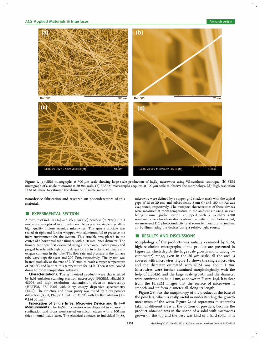
■ RESULTS AND DISCUSSIONSMorphology of the products was initially examined by SEM,high resolution micrographs of the product are presented inFigure 1a, which depicts the large scale growth and ultralong (∼centimeter) range, even in the 30 μm scale, all the area iscovered with microwires. Figure 1b shows the single microwire,and the diameter estimated with SEM was about 1 μm.Microwires were further examined morphologically with thehelp of FESEM and the large scale growth and the diameterwere confirmed to be ∼1 um, as shown in Figure 1c,d. It is clearfrom the FESEM images that the surface of microwires issmooth and uniform diameter all along its length.Figure 2 shows the morphology of the product at the base of
the powders, which is really useful in understanding the growthmechanism of the wires. Figure 2a−d represents micrographstaken at different areas at the bottom of powders, because theproduct obtained was in the shape of a solid with microwiresgrown on the top and the base was kind of a hard solid. This
Figure 1. (a) SEM micrographs at 300 μm scale showing large scale production of In2Se3 microwires using VS synthesis technique. (b) SEMmicrograph of a single microwire at 20 μm scale. (c) FESEM micrographs acquires at 100 μm scale to observe the morphology. (d) High resolutionFESEM image to estimate the diameter of single microwire.
ACS Applied Materials & Interfaces Research Article
dx.doi.org/10.1021/am501933p | ACS Appl. Mater. Interfaces 2014, 6, 9550−95569551

figure clearly suggests that at the start, the mixture of powdersfirst solidifies in the shape of bundles and chemical reactiontakes place at this stage. As the internal energy of the systemincreases because the product was placed at 700 °C for 24 h,these solid bundles break up into 1D structures. At the finalstage, these wires grow longer on the upper portion andbreakup from the solid bundles. Because no catalyst was usedfor fabrication, the vapor−solid (VS) growth mechanism isproposed for In2Se3 microwires. We have performed a numberof experiments in order to reduce the diameter of the wires bytuning experimental conditions and could only obtain thediameter of 1 μm.Material characterization of the as grown In2Se3 microwires
was conducted to determine the crystallographic phase and theresults are presented in Figure 3. Figure 3a shows the TEMimage of a single microwire, which shows the length in severalmicrometers. The inset of the figure presents the image at a 1μm scale showing the smooth surface of the as grown wires.The high resolution TEM (HRTEM) analysis (Figure 3b)
reveals the expected hexagonal lattice fringes with a latticespacing of 0.35 nm, consistent with the (110) plane in XRDspectrum highest intensity peak. The corresponding selectedarea electron diffraction (SAED) pattern is shown in Figure 3c.The SAED spot pattern confirms the hexagonal crystallinestructure of high quality. All the directions of the planes aremarked according to the d-spacing and angles as depicted from
XRD spectrum analysis. The SAED pattern clearly demon-strates that the microwires are not mixed phase but in fact highcrystalline in nature. There exists at least five different phases(α, β, γ, κ and δ) of stoichiometric In2Se3 with varying latticeparameters: α-phase, a = 4.02 Å, c = 19.23 Å;36 β-phase, a =4.01 Å, c = 19.22 Å;37 γ-phase, a = 7.12 Å, c = 19.38 Å;38 κ-phase, a = 8.09 Å, c = 19.85 Å;39 δ-phase, a = 4.00 Å, c = 19.28Å.40 Although, discrepancies do exist in the literature. Figure 3dshows the XRD spectrum of as-synthesized In2Se3 microwiresin furnace tube using elemental In and Se powders asprecursors. Millar indices of every peak are indexed in thefigure and it is observed that the main peaks located at 2θ =24.94, 27.54, 37.46, 43.90 and 52.54° corresponding to the(110), (006), (116), (207) and (306) planes, respectively, havethe highest intensity. All the peaks match well with the peaks ofhexagonal In2Se3 except one peak present at 2θ = 21° whichcorrespond to indium oxide. The slight extra amounts inindium powders present in the crucible might have beenconverted to indium oxide as the upper empty portion of thecrucible contained air before placing in the furnace tube.Although the tube was heavily flushed with high purity Ar, stillthere might be a chance of air trapping. The lattice parameterscalculated for hexagonal In2Se3 are a =7.1286 Å and c =19.3810Å, which correspond to the standard values of JCPDS card No.89-0658 for In2Se3. It is clearly evident from the crystallo-graphic lattice parameters that the γ-phase evolves as a result of
Figure 2. (a) SEM micrographs of the product at base showing large scale production in the form of bundles. (b) High resolution micrograph ofbundles. (c) SEM micrographs of bundles from the middle showing ultralong microwires. (d) Different view of bundle formation.
ACS Applied Materials & Interfaces Research Article
dx.doi.org/10.1021/am501933p | ACS Appl. Mater. Interfaces 2014, 6, 9550−95569552
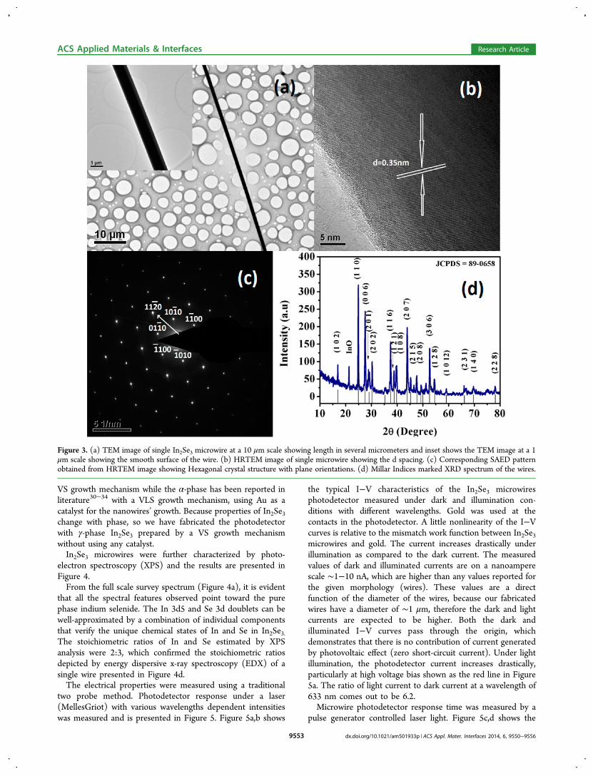
VS growth mechanism while the α-phase has been reported inliterature30−34 with a VLS growth mechanism, using Au as acatalyst for the nanowires’ growth. Because properties of In2Se3change with phase, so we have fabricated the photodetectorwith γ-phase In2Se3 prepared by a VS growth mechanismwithout using any catalyst.In2Se3 microwires were further characterized by photo-
electron spectroscopy (XPS) and the results are presented inFigure 4.From the full scale survey spectrum (Figure 4a), it is evident
that all the spectral features observed point toward the purephase indium selenide. The In 3d5 and Se 3d doublets can bewell-approximated by a combination of individual componentsthat verify the unique chemical states of In and Se in In2Se3.The stoichiometric ratios of In and Se estimated by XPSanalysis were 2:3, which confirmed the stoichiometric ratiosdepicted by energy dispersive x-ray spectroscopy (EDX) of asingle wire presented in Figure 4d.The electrical properties were measured using a traditional
two probe method. Photodetector response under a laser(MellesGriot) with various wavelengths dependent intensitieswas measured and is presented in Figure 5. Figure 5a,b shows
the typical I−V characteristics of the In2Se3 microwiresphotodetector measured under dark and illumination con-ditions with different wavelengths. Gold was used at thecontacts in the photodetector. A little nonlinearity of the I−Vcurves is relative to the mismatch work function between In2Se3microwires and gold. The current increases drastically underillumination as compared to the dark current. The measuredvalues of dark and illuminated currents are on a nanoamperescale ∼1−10 nA, which are higher than any values reported forthe given morphology (wires). These values are a directfunction of the diameter of the wires, because our fabricatedwires have a diameter of ∼1 μm, therefore the dark and lightcurrents are expected to be higher. Both the dark andilluminated I−V curves pass through the origin, whichdemonstrates that there is no contribution of current generatedby photovoltaic effect (zero short-circuit current). Under lightillumination, the photodetector current increases drastically,particularly at high voltage bias shown as the red line in Figure5a. The ratio of light current to dark current at a wavelength of633 nm comes out to be 6.2.Microwire photodetector response time was measured by a
pulse generator controlled laser light. Figure 5c,d shows the
Figure 3. (a) TEM image of single In2Se3 microwire at a 10 μm scale showing length in several micrometers and inset shows the TEM image at a 1μm scale showing the smooth surface of the wire. (b) HRTEM image of single microwire showing the d spacing. (c) Corresponding SAED patternobtained from HRTEM image showing Hexagonal crystal structure with plane orientations. (d) Millar Indices marked XRD spectrum of the wires.
ACS Applied Materials & Interfaces Research Article
dx.doi.org/10.1021/am501933p | ACS Appl. Mater. Interfaces 2014, 6, 9550−95569553
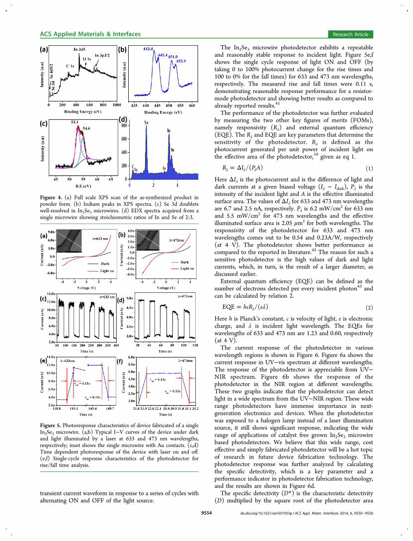
transient current waveform in response to a series of cycles withalternating ON and OFF of the light source.
The In2Se3 microwire photodetector exhibits a repeatableand reasonably stable response to incident light. Figure 5e,fshows the single cycle response of light ON and OFF (bytaking 0 to 100% photocurrent change for the rise times and100 to 0% for the fall times) for 633 and 473 nm wavelengths,respectively. The measured rise and fall times were 0.11 s,demonstrating reasonable response performance for a resistor-mode photodetector and showing better results as compared toalready reported results.41
The performance of the photodetector was further evaluatedby measuring the two other key figures of merits (FOMs),namely responsivity (Rλ) and external quantum efficiency(EQE). The Rλ and EQE are key parameters that determine thesensitivity of the photodetector. Rλ is defined as thephotocurrent generated per unit power of incident light onthe effective area of the photodetector,10 given as eq 1.
= Δλ λ λR P AI /( ) (1)
Here ΔIλ is the photocurrent and is the difference of light anddark currents at a given biased voltage (Iλ − Idark), Pλ is theintensity of the incident light and A is the effective illuminatedsurface area. The values of ΔIλ for 633 and 473 nm wavelengthsare 6.7 and 2.5 nA, respectively. Pλ is 6.2 mW/cm2 for 633 nmand 5.5 mW/cm2 for 473 nm wavelengths and the effectiveilluminated surface area is 2.05 μm2 for both wavelengths. Theresponsivity of the photodetector for 633 and 473 nmwavelengths comes out to be 0.54 and 0.23A/W, respectively(at 4 V). The photodetector shows better performance ascompared to the reported in literature.42 The reason for such asensitive photodetector is the high values of dark and lightcurrents, which, in turn, is the result of a larger diameter, asdiscussed earlier.External quantum efficiency (EQE) can be defined as the
number of electrons detected per every incident photon43 andcan be calculated by relation 2.
λ= λhcR eEQE /( ) (2)
Here h is Planck’s constant, c is velocity of light, e is electroniccharge, and λ is incident light wavelength. The EQEs forwavelengths of 633 and 473 nm are 1.23 and 0.60, respectively(at 4 V).The current response of the photodetector in various
wavelength regions is shown in Figure 6. Figure 6a shows thecurrent response in UV−vis spectrum at different wavelengths.The response of the photodetector is appreciable from UV−NIR spectrum. Figure 6b shows the response of thephotodetector in the NIR region at different wavelengths.These two graphs indicate that the photodetector can detectlight in a wide spectrum from the UV−NIR region. These widerange photodetectors have immense importance in next-generation electronics and devices. When the photodetectorwas exposed to a halogen lamp instead of a laser illuminationsource, it still shows significant response, indicating the widerange of applications of catalyst free grown In2Se3 microwirebased photodetectors. We believe that this wide range, costeffective and simply fabricated photodetector will be a hot topicof research in future device fabrication technology. Thephotodetector response was further analyzed by calculatingthe specific detectivity, which is a key parameter and aperformance indicator in photodetector fabrication technology,and the results are shown in Figure 6d.The specific detectivity (D*) is the characteristic detectivity
(D) multiplied by the square root of the photodetector area
Figure 4. (a) Full scale XPS scan of the as-synthesized product inpowder form. (b) Indium peaks in XPS spectra. (c) Se 3d doubletswell-resolved in In2Se3 microwires. (d) EDX spectra acquired from asingle microwire showing stoichiometric ratios of In and Se of 2:3.
Figure 5. Photoresponse characteristics of device fabricated of a singleIn2Se3 microwire. (a,b) Typical I−V curves of the device under darkand light illuminated by a laser at 633 and 473 nm wavelengths,respectively; inset shows the single microwire with Au contacts. (c,d)Time dependent photoresponse of the device with laser on and off.(e,f) Single-cycle response characteristics of the photodetector forrise/fall time analysis.
ACS Applied Materials & Interfaces Research Article
dx.doi.org/10.1021/am501933p | ACS Appl. Mater. Interfaces 2014, 6, 9550−95569554

(A) (D* = D√A). Here D is the inverse of noise-equivalentpower (NEP). The NEP, defined as the minimum input opticalpower to generate photocurrent equal to the RMS noisecurrent in 1 Hz bandwidth,44 is essentially the minimumdetectable signal. The specific detectivity allows differentsystems to be compared independent of device area and bandwidth. The specific detectivity (D*) in the unit of Jones wascalculated using D* = RλA
1/2/(2eIdark)1/2, where Rλ is the
responsivity, A is the device effective area and Idark is the darkcurrent.45 The specific detectivity (at 4 V) was calculated to be∼3.94 × 10¹⁰ Jones at 633 nm and 1.67 × 10¹⁰ Jones at 473 nmwavelengths, respectively. Figure 6d shows the EQE andspecific detectivity at each wavelength under monochromaticillumination and demonstrates the reasonable response fromcatalyst free grown In2Se3 single microwire based photo-detectors.
■ CONCLUSIONFor the first time, we present the synthesis of high qualityIn2Se3 microwires by a vapor−solid approach without using anycatalyst and demonstrate the photoconductive characteristics ofan individual microwire. The high quality microwires aresynthesized on a large scale and single crystalline in nature. Thewires have a uniform diameter of ∼1 μm and length of severalmicrometers. These ultralong wires have never been reportedto date. The photodetector based on catalyst free grownmicrowires possess fast, reversible and stable photoresponsewhen exposed to different wavelengths of light. To investigatethe performance of the photodetector, the key figure of meritswere calculated. The photodetector exhibits a photoresponsiv-ity of 0.54 A/W and an external quantum efficiency (EQE) of1.23 at 633 nm with 4 V bias. The photodetector has areasonable response time of 0.11 s and a specific detectivity of3.94 × 1010 Jones at 633 nm with a light detection range from350 to 1050 nm. The results indicate that the catalyst freegrowth mechanism for In2Se3 microwires with high quality andsingle-crystallographic phase has immense potential in futuredevices such as UV−vis-NIR detectors, biomedical imaging,high-resolution video recording, astronomy and photovoltaics.
■ AUTHOR INFORMATION
Corresponding Author*Chuanbao Cao. E-mail: [email protected]. Tel: +86 1068913792. Fax: +86 10 68912001.
NotesThe authors declare no competing financial interest.
■ ACKNOWLEDGMENTS
This work was supported by National Natural ScienceFoundation of China (21371023, 50972017) and the ResearchFund for the Doctoral Program of Higher Education of China(20101101110026)
■ REFERENCES(1) Fang, X. S.; Bando, Y.; Liao, M. Y.; Zhai, T. Y.; Gautam, U. K.; Li,L.; Koide, Y.; Golberg, D. An Efficient Way to Assemble ZnSNanobelts as Ultraviolet-Light Sensors with Enhanced Photocurrentand Stability. Adv. Funct. Mater. 2010, 20, 500−508.(2) Zhai, T. Y.; Fang, X. S.; Bando, Y.; Dierre, B.; Liu, B. D.; Zeng, H.B.; Huang, Y.; Xu, X. J.; Yuan, X. L.; Sekiguchi, T.; Golberg, D.Characterization, Cathodoluminescence, and Field-Emission Proper-ties of Morphology-Tunable CdS Micro/Nanostructures. Adv. Funct.Mater. 2009, 19, 2423−30.(3) Fang, X. S.; Xiong, S. L.; Zhai, T. Y.; Bando, Y.; Liao, M. Y.;Gautam, U. K.; Koide, Y.; Zhang, X. G.; Qian, Y. T.; Golberg, D. High-Performance Bule/Ultraviolet-Light-Sensitive ZnSe-Nanobelt Photo-detectors. Adv. Mater. 2009, 21, 5016−5021.(4) Pan, Z. W.; Dai, Z. R.; Wang, Z. L. Nanobelts of SemiconductingOxides. Science 2001, 291, 1947−49.(5) Zhai, T. Y.; Zhong, H. Z.; Gu, Z. J.; Peng, A. D.; Fu, H. B.; Ma,Y.; Li, Y. F.; Yao, J. N. Manipulation of the Morphology of ZnSeSubmicron Structures Using CdSe Nanocrystals as the Seeds. J. Phys.Chem. C 2007, 111, 2980−86.(6) Ye, C. H.; Fang, X. S.; Hao, Y. F.; Teng, X. M.; Zhang, L. D. ZincOxide Nanostructures: Morphology Derivation and Evolution. J. Phys.Chem. B 2005, 109, 19758−65.(7) Ali, Z.; Cao, C. B.; Li, L. J.; Wang, Y. L.; Cao, T.; Tahir, M.;Idrees, F.; Butt, F. K. Effect of Synthesis Technique on Electro-chemical Performance of Bismuth Selenide. J. Power Sources 2013, 29,216−212.(8) Ali, Z.; Cao, C. B.; Khan, W. S.; Butt, F. K.; Hussain, S.;Mahmood, T.; Nabi, G.; Usman, Z. Simultaneous Growth of ZnSeCactus-Like Structures and Novel Microflowers of Selenium. J. AlloysCompd. 2012, 513, 620−625.(9) Xuelian, Y.; Cao, C. B.; Zhu, H. S. Synthesis and Photo-luminescence Properties of Bi2S3 Nanowires via Surfactant Micelle-Template Inducing Reaction. Solid. State Commun. 2005, 134, 239−243.(10) Zhai, T. Y.; Fang, X. S.; Liao, M. Y.; Xu, X. J.; Li, L.; Liu, B. D.;Koide, Y.; Ma, Y.; Yao, J.; Bando, Y.; Golberg, D. Fabrication of High-Quality In2Se3 Nanowire Arrays toward High-Performance Visible-Light Photodetectors. ACS Nano 2010, 4, 1596−1602.(11) Jie, J. S.; Zhang, W. J.; Jiang, Y.; Meng, X. M.; Li, Y. Q.; Lee, S.T. Photoconductive Characteristics of Single-Crystal CdS Nanorib-bons. Nano Lett. 2006, 6, 1887−92.(12) Lin, D. D.; Wu, H.; Pan, W. Photoswitches and MemoriesAssembled by Electrospinning Aluminum-Doped Zinc Oxide SingleNanowires. Adv. Mater. 2007, 19, 3968−72.(13) Xuelian, Y.; Cao, C. B. Photoresponse and Field-EmissionProperties of Bismuth Sulfide Nanoflowers. Cryst. Growth Des. 2008, 8,3951−3955.(14) Butt, F. K.; Mirza, M.; Cao, C.B.; Idrees, F.; Tahir, M.; Safdar,M.; Ali, Z.; Tanveer, M.; Aslam, I. Synthesis of Mid-Infrared SnSeNanowires and their Optoelectronic Properties. CrystEngComm 2014,16, 3470−3473.
Figure 6. (a) Photoresponse of the photodetector at differentwavelengths showing UV−vis range. (b) Photoresponse at NIRregion. (c) Photoresponse at different intensities of halogen lamp. (d)EQE and specific detectivity curves showing the sensitivity of thedetector.
ACS Applied Materials & Interfaces Research Article
dx.doi.org/10.1021/am501933p | ACS Appl. Mater. Interfaces 2014, 6, 9550−95569555

(15) Jiang, Y.; Zhang, W. J.; Jie, J. S.; Meng, X. M.; Fan, X.; Lee, S. T.Photoresponse Properties of CdSe Single-Nanoribbon Photodetectors.Adv. Funct. Mater. 2007, 17, 1795−1800.(16) Liao, M. Y.; Koide, Y.; Alvarez, J.; Imura, M.; Kleider, J. P.Persistent Positive and Transient Absolute Negative PhtoconductivityObserved in Diamond Photodetectors. Phys. Rev. B 2008, 78, 045112−19.(17) Zhai, T. Y.; Fang, X. S.; Liao, M. Y.; Xu, X. J.; Zeng, H. B.;Bando, Y.; Golberg, D. Comprehensive Review of One-DimensionalMetal-Oxide Nanostructure Photodetectors. Sensors 2009, 9, 6504−29.(18) Julien, C.; Hatzikraniotis, E.; Kambas, K. Electrical Transport-Properties of Impurity-Doped In2Se3. Phys. Status Solidi A 1986, 97,579−585.(19) Shen, G. Z.; Chen, D.; Chen, P. C.; Zhou, C. W. Vapor-SolidGrowth of One-Dimensional Layer-Structured Gallium SulfideNanostructures. ACS Nano 2009, 3, 1115−1120.(20) Lyu, D. Y.; Lin, T. Y.; Lin, J. H.; Tseng, S. C.; Hwang, J. S.;Chiang, H. P.; Chiang, C. C.; Lan, S. M. Growth and Properties ofSingle-Phase γ-In2Se3 Thin Films on (111) Si Substrate by AP-MOCVD using H2Se Precursor. Sol. Energy Mater. Sol. Cells 2007, 91,888−92.(21) Peng, H. L.; Schoen, D. T.; Meister, S.; Zheng, X. F.; Cui, Y. J.Synthesis and Phase Transformation of In2Se3 and CuInSe2 Nano-wires. J. Am. Chem. Soc. 2007, 129, 34−35.(22) Vaidyanathan, R.; Stickney, J. L.; Cox, S. M.; Compton, S. P.;Happek, U. Formation of In2Se3 Thin Films and Nanostructures UsingElectrochemical Atomic Layer Epitaxy. J. Electroanal. Chem. 2003, 559,55−61.(23) Lai, K. J.; Peng, H. L.; Kundhikanjana, W.; Schoen, D. T.; Xie,C.; Meister, S.; Cui, Y.; Kelly, M. A.; Shen, Z. X. Nanoscale ElectronicInhomogeneity in In2Se3 Nanoribbons Revealed by MicrowaveImpedance Microscopy. Nano Lett. 2009, 9, 1265−69.(24) Peng, H. L.; Xie, C.; Schoen, D. T.; Cui, Y. Large Anisotropy ofElectrical Properties in Layer-Structured In2Se3 Nanowires. Nano Lett.2008, 8, 1511−16.(25) Yu, B.; Ju, S.; Sun, X. H.; Ng, G.; Nguyen, T. D.; Meyyappan,M.; Janes, D. B. Indium Selenide Nanowire Phase-Charge Memory.Appl. Phys. Lett. 2007, 91, 133119−21.(26) Chang, K. J.; Lahn, S. M.; Chang, J. Y. Growth of Single-Phaseby Using Metal Organic Chemical Vapor Deposition with Dual-SourcePrecursors. Appl. Phys. Lett. 2006, 89, 182118−21.(27) Cheon, J. W.; Arnold, J.; Yu, K. M.; Bourret, E. D. MetalorganicChemical Vapor Deposition of Semiconducting III/VI In2Se3 ThinFilms from the Single-Source Precursor: In[SeC(SiMe3)3]3. Chem.Mater. 1995, 7, 2273−76.(28) De Groot, C. H.; Moodera, J. S. Growth and Characterization ofa Novel In2Se3 Structure. J. Appl. Phys. 2001, 89, 4336−40.(29) Stoll, S. L.; Barron, A. R. Metal-Organic Chemical VaporDeposition of Indium Selenide (InSe) thin Films. Chem. Mater. 1998,10, 650−57.(30) Schoen, D. T.; Peng, H.; Cui, Y. Anisotropy of ChemicalTransformation from In2Se3 to CuInSe2 Nanowires through SolidState Reaction. J. Am. Chem. Soc. 2009, 131, 7973−7975.(31) Mafi, E.; Soudi, A.; Gu, Y. Electronically Driven Amorphizationin Phase-Change In2Se3 Nanowires. J. Phys. Chem. C 2012, 116,22539−22544.(32) Sun, X. H.; Yu, B.; Garrick, N. G.; Nguyen, T. D.; Meyyappan,M. III-VI Compound Semiconductor Indium Selenide (In2Se3)Nanowires: Synthesis and Characterization. Appl. Phys. Lett. 2006,89, 233121−23.(33) Baek, C. K.; Kang, D. G.; Kim, J. S.; Jin, B.; Rim, T.; Park, S. Y.;Meyyappan, M.; Jeong, Y. H.; Lee, J. S. Improved Performance ofIn2Se3 Nanowire Phase-Change Memory with SiO2 Passivation. Solid-State Electron. 2013, 80, 10−13.(34) Li, Y.; Gao, J.; Li, Q. L.; Peng, M. F.; Sun, X. H.; Li, Y. Y.; Yuan,G.; Wen, W.; Meyyappan, M. J. Thermal Phase Transformation ofIn2Se3Nanowires Studied by in situ Synchrotron Radiation X-rayDiffraction. Mater. Chem. 2011, 21, 6944−6947.
(35) Wang, J. J.; Cao, F. F.; Jiang, L.; Guo, Y. G.; Hu, W. P.; Wan, L.J. High Performance Photodetectors of Individual InSe SingleCrystalline Nanowire. J. Am. Chem. Soc. 2009, 131, 15602−15603.(36) Popovic, S.; Tonejc, A.; Grzeta-Plenkovic, B.; Celustka, B.;Trojko, R. Revised and New Crystal Data for Indium Selenides. J.Appl. Crystallogr. 1979, 12, 416−420.(37) Lutz, H.; Fischer, M.; Baldus, H.-P.; Blachnik, R. ZurPolymorphie des In2Se3. J. Less-Common Met. 1988, 143, 83−92.(38) Pfitzner, A.; Lutz, H. D. Redetermination of the CrystalStructure of Gamma-In2Se3 by Twin Crystal X-Ray Method. J. SolidState Chem. 1996, 124, 305−308.(39) Jasinski, J.; Swider, W.; Washburn, J.; Liliental-Weber, Z.;Chaiken, A.; Nauka, K.; Gibson, G. A.; Yang, C. C. Crystal Structure ofk-In2Se3. Appl. Phys. Lett. 2002, 81, 4356−4358.(40) Drapak, S. I.; Kovalyuk, Z. D. Asymmetric Current Flow in aNative Oxide/Indium Selenide Heterostructure. Inorg. Mater. 2011,47, 1178−1182.(41) Zhai, T. Y.; Ma, Y.; Li, L.; Fang, X. S.; Liao, M. Y.; Koide, Y.;Yao, J. N.; Bando, Y.; Goldberg, D. Morphology-tunableIn2Se3Nanostructures with Enhanced Electrical and PhotoelectricalPerformances via Sulfur Doping. Mater. Chem. 2010, 20, 6630−6637.(42) Zhai, T. Y.; Fang, X. S.; Liao, M. Y.; Xu, X. J.; Li, L.; Liu, B. D.;Koide, Y.; Ma, Y.; Yao, J. N.; Bando, Y.; Golberg, D. Fabrication ofHigh-Quality In2Se3Nanowire Arrays Towards High-PerformanceVisible-Light Photodetectors. ACS Nano 2010, 4, 1596−1602.(43) Wang, Z. X.; Safdar, M.; Jiang, C.; He, J. High-Performance UVVisible NIR Broad Spectral Photodetectors Based on One-Dimen-sional In2Te3 Nanostructures. Nano Lett. 2012, 12, 4715−4721.(44) Li, Q. L.; Li, Y.; Gao, J.; Wang, S. D.; Sun, X. H. HighPerformance Single In2Se3Nanowire Photodetector. Appl. Phys. Lett.2011, 99, 243105−08.(45) Hu, P.; Wang, L.; Yoon, M.; Zhang, J.; Feng, W.; Wang, X.;Wen, Z.; Idrobo, J. C.; Miyamoto, Y.; Geohegan, D. B. HighlyResponsive Ultrathin GaS Nanosheet Photodetectors on Rigid andFlexible Substrates. Nano Lett. 2013, 13, 1649−1654.
ACS Applied Materials & Interfaces Research Article
dx.doi.org/10.1021/am501933p | ACS Appl. Mater. Interfaces 2014, 6, 9550−95569556
Copyright © 2022 FDOKUMEN