Synthesis and characterization of cadmium selenide nanostructures on porous aluminum oxide templates...
7
Synthesis and characterization of cadmium selenide nanostructures on porous aluminum oxide templates by high frequency alternating current electrolysis P. Ram Sankar a, *, Pragya Tiwari a , Ravi Kumar a , Tapas Ganguli a , C. Mukherjee a , A.K. Srivastava a , S.M. Oak a , Rajesh K. Pathak b a Raja Ramanna Centre for Advanced Technology, Indore 452 013, India b Department of Chemistry, Government Holkar Science College, Indore, India 1. Introduction Nanostructured materials are drawing much attention due to their potential applications in electronic, optical and magnetic devices [1]. Metals and semiconductor films, wires and particles with nanoscale dimensions show novel electronic, optical and chemical behavior due to quantum confinement of electrons [2]. Several techniques ranging from epitaxial growth to chemical and lithographic methods are available for preparing nanostructured materials. The shape and size of nanostructures formed depend on the method used for synthesizing and their operating conditions. Significant progress has already been made in the field of zero- and two-dimensional nanostructures such as quantum dots and quantum wells respectively [3]. Synthesis of one-dimensional nanoscale structures such as nanowires, nanorods and nanotubes is of considerable interest due to their applications in the field of catalysis, electrochemistry, energy storage, nanoelectronics and optoelectronics [1,4]. Template based synthesis of nanomaterials is a versatile and simple approach for the preparation of one- dimensional metal nanowires and tubes [5]. Tracketch polymeric membranes and porous alumina are generally used as templates for the deposition of metals and semiconductors [6]. Porous aluminum oxide is obtained by anodic oxidation of aluminum in a solution of sulfuric, oxalic or phosphoric acid [7–10]. The diameter and length of the pores can be altered by modifying the operating conditions such as anodizing time, temperature and concentration of the electrolyte. The pores in anodic alumina are uniform, parallel and open only at the oxide–electrolyte interface. Self-organized formation of hexagonal pores is due to the development of repulsive forces between neighboring pores. These repulsive forces are created because of mechanical stress developed by expansion of aluminum due to oxide formation [11]. It has been shown that metallic nanowires of nickel [12], cobalt [12,14], copper [13], iron [14] and molybdenum [15] can be formed by electrochemically depositing respective metal into the pores. Development of thin nanostructured semiconductor films has potential applications in chemical sensors, microelectronics, electrooptics imaging science, photovoltaics and photocatalysis. Applied Surface Science 256 (2010) 2097–2103 ARTICLE INFO Article history: Received 2 May 2009 Received in revised form 15 September 2009 Accepted 15 September 2009 Available online 24 September 2009 PACS: 81.16c 82.45Aa Keywords: Anodic oxide template High frequency alternating current Cadmium selenide End standing nanostrips Optical studies Band gap Quantum confinement ABSTRACT We have successfully deposited nanostructured cadmium selenide (CdSe) inside anodic aluminum oxide (AAO) templates from aqueous electrolyte containing cadmium sulfate, selenium oxide and mercuric chloride by using high frequency alternating current (19 V rms , 200 Hz). Addition of mercury ions aids in the deposition of CdSe inside anodic oxide pores. Scanning and transmission electron microscopy studies of the deposit etched in phosphoric acid showed the presence of end standing nanostrips. Energy dispersive X-ray analysis of the deposit confirmed the presence of cadmium and selenium in the deposit. X-ray diffraction (XRD) studies of the deposit showed small but broad diffraction peaks consistent with the presence of hexagonal CdSe. Optical studies revealed blue shift in band gap energy due to quantum confinement. ß 2009 Elsevier B.V. All rights reserved. * Corresponding author at: Chemical Treatment Laboratory, Raja Ramanna Centre for Advanced Technology, RRCAT Post, Indore 452 013, Madhya Pradesh, India. Tel.: +91 731 2488092; fax: +91 731 2488091. E-mail address: [email protected] (P.R. Sankar). Contents lists available at ScienceDirect Applied Surface Science journal homepage: www.elsevier.com/locate/apsusc 0169-4332/$ – see front matter ß 2009 Elsevier B.V. All rights reserved. doi:10.1016/j.apsusc.2009.09.054
-
Upload
independent -
Category
Documents
-
view
0 -
download
0
Transcript of Synthesis and characterization of cadmium selenide nanostructures on porous aluminum oxide templates...
Synthesis and characterization of cadmium selenide nanostructures on porousaluminum oxide templates by high frequency alternating current electrolysis
P. Ram Sankar a,*, Pragya Tiwari a, Ravi Kumar a, Tapas Ganguli a, C. Mukherjee a,A.K. Srivastava a, S.M. Oak a, Rajesh K. Pathak b
a Raja Ramanna Centre for Advanced Technology, Indore 452 013, Indiab Department of Chemistry, Government Holkar Science College, Indore, India
Applied Surface Science 256 (2010) 2097–2103
A R T I C L E I N F O
Article history:
Received 2 May 2009
Received in revised form 15 September 2009
Accepted 15 September 2009
Available online 24 September 2009
PACS:
81.16c
82.45Aa
Keywords:
Anodic oxide template
High frequency alternating current
Cadmium selenide
End standing nanostrips
Optical studies
Band gap
Quantum confinement
A B S T R A C T
We have successfully deposited nanostructured cadmium selenide (CdSe) inside anodic aluminum oxide
(AAO) templates from aqueous electrolyte containing cadmium sulfate, selenium oxide and mercuric
chloride by using high frequency alternating current (19 Vrms, 200 Hz). Addition of mercury ions aids in
the deposition of CdSe inside anodic oxide pores. Scanning and transmission electron microscopy studies
of the deposit etched in phosphoric acid showed the presence of end standing nanostrips. Energy
dispersive X-ray analysis of the deposit confirmed the presence of cadmium and selenium in the deposit.
X-ray diffraction (XRD) studies of the deposit showed small but broad diffraction peaks consistent with
the presence of hexagonal CdSe. Optical studies revealed blue shift in band gap energy due to quantum
confinement.
� 2009 Elsevier B.V. All rights reserved.
Contents lists available at ScienceDirect
Applied Surface Science
journa l homepage: www.e lsev ier .com/ locate /apsusc
1. Introduction
Nanostructured materials are drawing much attention due totheir potential applications in electronic, optical and magneticdevices [1]. Metals and semiconductor films, wires and particleswith nanoscale dimensions show novel electronic, optical andchemical behavior due to quantum confinement of electrons [2].Several techniques ranging from epitaxial growth to chemical andlithographic methods are available for preparing nanostructuredmaterials. The shape and size of nanostructures formed depend onthe method used for synthesizing and their operating conditions.Significant progress has already been made in the field of zero- andtwo-dimensional nanostructures such as quantum dots andquantum wells respectively [3]. Synthesis of one-dimensionalnanoscale structures such as nanowires, nanorods and nanotubesis of considerable interest due to their applications in the field of
* Corresponding author at: Chemical Treatment Laboratory, Raja Ramanna
Centre for Advanced Technology, RRCAT Post, Indore 452 013, Madhya Pradesh,
India. Tel.: +91 731 2488092; fax: +91 731 2488091.
E-mail address: [email protected] (P.R. Sankar).
0169-4332/$ – see front matter � 2009 Elsevier B.V. All rights reserved.
doi:10.1016/j.apsusc.2009.09.054
catalysis, electrochemistry, energy storage, nanoelectronics andoptoelectronics [1,4]. Template based synthesis of nanomaterials isa versatile and simple approach for the preparation of one-dimensional metal nanowires and tubes [5]. Tracketch polymericmembranes and porous alumina are generally used as templatesfor the deposition of metals and semiconductors [6]. Porousaluminum oxide is obtained by anodic oxidation of aluminum in asolution of sulfuric, oxalic or phosphoric acid [7–10]. The diameterand length of the pores can be altered by modifying the operatingconditions such as anodizing time, temperature and concentrationof the electrolyte. The pores in anodic alumina are uniform, paralleland open only at the oxide–electrolyte interface. Self-organizedformation of hexagonal pores is due to the development ofrepulsive forces between neighboring pores. These repulsive forcesare created because of mechanical stress developed by expansionof aluminum due to oxide formation [11]. It has been shown thatmetallic nanowires of nickel [12], cobalt [12,14], copper [13], iron[14] and molybdenum [15] can be formed by electrochemicallydepositing respective metal into the pores.
Development of thin nanostructured semiconductor films haspotential applications in chemical sensors, microelectronics,electrooptics imaging science, photovoltaics and photocatalysis.
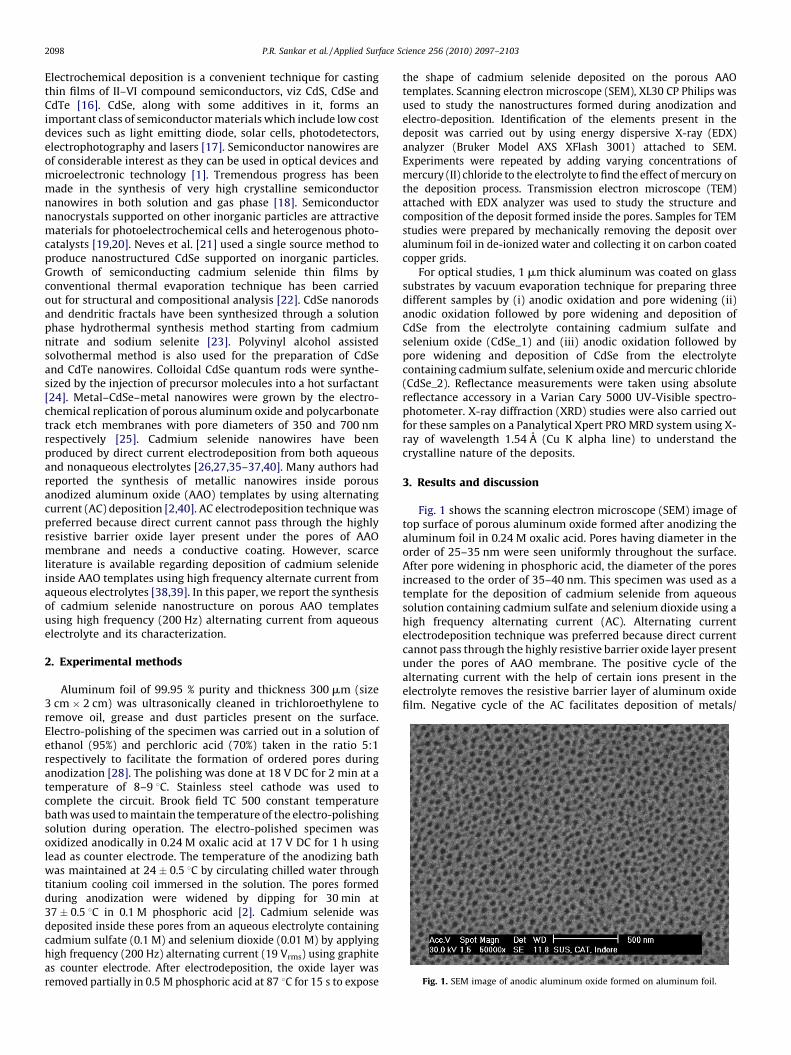
Fig. 1. SEM image of anodic aluminum oxide formed on aluminum foil.
P.R. Sankar et al. / Applied Surface Science 256 (2010) 2097–21032098
Electrochemical deposition is a convenient technique for castingthin films of II–VI compound semiconductors, viz CdS, CdSe andCdTe [16]. CdSe, along with some additives in it, forms animportant class of semiconductor materials which include low costdevices such as light emitting diode, solar cells, photodetectors,electrophotography and lasers [17]. Semiconductor nanowires areof considerable interest as they can be used in optical devices andmicroelectronic technology [1]. Tremendous progress has beenmade in the synthesis of very high crystalline semiconductornanowires in both solution and gas phase [18]. Semiconductornanocrystals supported on other inorganic particles are attractivematerials for photoelectrochemical cells and heterogenous photo-catalysts [19,20]. Neves et al. [21] used a single source method toproduce nanostructured CdSe supported on inorganic particles.Growth of semiconducting cadmium selenide thin films byconventional thermal evaporation technique has been carriedout for structural and compositional analysis [22]. CdSe nanorodsand dendritic fractals have been synthesized through a solutionphase hydrothermal synthesis method starting from cadmiumnitrate and sodium selenite [23]. Polyvinyl alcohol assistedsolvothermal method is also used for the preparation of CdSeand CdTe nanowires. Colloidal CdSe quantum rods were synthe-sized by the injection of precursor molecules into a hot surfactant[24]. Metal–CdSe–metal nanowires were grown by the electro-chemical replication of porous aluminum oxide and polycarbonatetrack etch membranes with pore diameters of 350 and 700 nmrespectively [25]. Cadmium selenide nanowires have beenproduced by direct current electrodeposition from both aqueousand nonaqueous electrolytes [26,27,35–37,40]. Many authors hadreported the synthesis of metallic nanowires inside porousanodized aluminum oxide (AAO) templates by using alternatingcurrent (AC) deposition [2,40]. AC electrodeposition technique waspreferred because direct current cannot pass through the highlyresistive barrier oxide layer present under the pores of AAOmembrane and needs a conductive coating. However, scarceliterature is available regarding deposition of cadmium selenideinside AAO templates using high frequency alternate current fromaqueous electrolytes [38,39]. In this paper, we report the synthesisof cadmium selenide nanostructure on porous AAO templatesusing high frequency (200 Hz) alternating current from aqueouselectrolyte and its characterization.
2. Experimental methods
Aluminum foil of 99.95 % purity and thickness 300 mm (size3 cm � 2 cm) was ultrasonically cleaned in trichloroethylene toremove oil, grease and dust particles present on the surface.Electro-polishing of the specimen was carried out in a solution ofethanol (95%) and perchloric acid (70%) taken in the ratio 5:1respectively to facilitate the formation of ordered pores duringanodization [28]. The polishing was done at 18 V DC for 2 min at atemperature of 8–9 8C. Stainless steel cathode was used tocomplete the circuit. Brook field TC 500 constant temperaturebath was used to maintain the temperature of the electro-polishingsolution during operation. The electro-polished specimen wasoxidized anodically in 0.24 M oxalic acid at 17 V DC for 1 h usinglead as counter electrode. The temperature of the anodizing bathwas maintained at 24 � 0.5 8C by circulating chilled water throughtitanium cooling coil immersed in the solution. The pores formedduring anodization were widened by dipping for 30 min at37 � 0.5 8C in 0.1 M phosphoric acid [2]. Cadmium selenide wasdeposited inside these pores from an aqueous electrolyte containingcadmium sulfate (0.1 M) and selenium dioxide (0.01 M) by applyinghigh frequency (200 Hz) alternating current (19 Vrms) using graphiteas counter electrode. After electrodeposition, the oxide layer wasremoved partially in 0.5 M phosphoric acid at 87 8C for 15 s to expose
the shape of cadmium selenide deposited on the porous AAOtemplates. Scanning electron microscope (SEM), XL30 CP Philips wasused to study the nanostructures formed during anodization andelectro-deposition. Identification of the elements present in thedeposit was carried out by using energy dispersive X-ray (EDX)analyzer (Bruker Model AXS XFlash 3001) attached to SEM.Experiments were repeated by adding varying concentrations ofmercury (II) chloride to the electrolyte to find the effect of mercury onthe deposition process. Transmission electron microscope (TEM)attached with EDX analyzer was used to study the structure andcomposition of the deposit formed inside the pores. Samples for TEMstudies were prepared by mechanically removing the deposit overaluminum foil in de-ionized water and collecting it on carbon coatedcopper grids.
For optical studies, 1 mm thick aluminum was coated on glasssubstrates by vacuum evaporation technique for preparing threedifferent samples by (i) anodic oxidation and pore widening (ii)anodic oxidation followed by pore widening and deposition ofCdSe from the electrolyte containing cadmium sulfate andselenium oxide (CdSe_1) and (iii) anodic oxidation followed bypore widening and deposition of CdSe from the electrolytecontaining cadmium sulfate, selenium oxide and mercuric chloride(CdSe_2). Reflectance measurements were taken using absolutereflectance accessory in a Varian Cary 5000 UV-Visible spectro-photometer. X-ray diffraction (XRD) studies were also carried outfor these samples on a Panalytical Xpert PRO MRD system using X-ray of wavelength 1.54 A (Cu K alpha line) to understand thecrystalline nature of the deposits.
3. Results and discussion
Fig. 1 shows the scanning electron microscope (SEM) image oftop surface of porous aluminum oxide formed after anodizing thealuminum foil in 0.24 M oxalic acid. Pores having diameter in theorder of 25–35 nm were seen uniformly throughout the surface.After pore widening in phosphoric acid, the diameter of the poresincreased to the order of 35–40 nm. This specimen was used as atemplate for the deposition of cadmium selenide from aqueoussolution containing cadmium sulfate and selenium dioxide using ahigh frequency alternating current (AC). Alternating currentelectrodeposition technique was preferred because direct currentcannot pass through the highly resistive barrier oxide layer presentunder the pores of AAO membrane. The positive cycle of thealternating current with the help of certain ions present in theelectrolyte removes the resistive barrier layer of aluminum oxidefilm. Negative cycle of the AC facilitates deposition of metals/
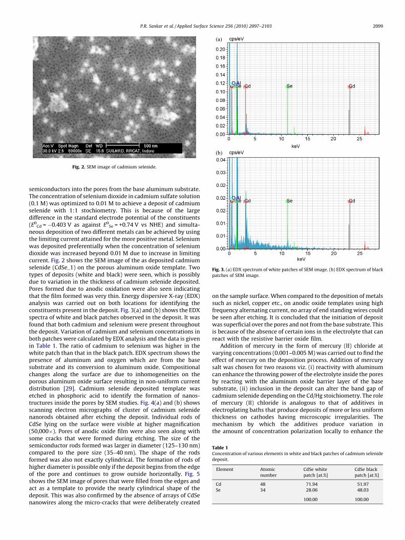
Fig. 2. SEM image of cadmium selenide.
Fig. 3. (a) EDX spectrum of white patches of SEM image. (b) EDX spectrum of black
patches of SEM image.
Table 1Concentration of various elements in white and black patches of cadmium selenide
deposit.
Element Atomic
number
CdSe white
patch [at.%]
CdSe black
patch [at.%]
Cd 48 71.94 51.97
Se 34 28.06 48.03
100.00 100.00
P.R. Sankar et al. / Applied Surface Science 256 (2010) 2097–2103 2099
semiconductors into the pores from the base aluminum substrate.The concentration of selenium dioxide in cadmium sulfate solution(0.1 M) was optimized to 0.01 M to achieve a deposit of cadmiumselenide with 1:1 stochiometry. This is because of the largedifference in the standard electrode potential of the constituents(E0
Cd = �0.403 V as against E0Se = +0.74 V vs NHE) and simulta-
neous deposition of two different metals can be achieved by usingthe limiting current attained for the more positive metal. Seleniumwas deposited preferentially when the concentration of seleniumdioxide was increased beyond 0.01 M due to increase in limitingcurrent. Fig. 2 shows the SEM image of the as deposited cadmiumselenide (CdSe_1) on the porous aluminum oxide template. Twotypes of deposits (white and black) were seen, which is possiblydue to variation in the thickness of cadmium selenide deposited.Pores formed due to anodic oxidation were also seen indicatingthat the film formed was very thin. Energy dispersive X-ray (EDX)analysis was carried out on both locations for identifying theconstituents present in the deposit. Fig. 3(a) and (b) shows the EDXspectra of white and black patches observed in the deposit. It wasfound that both cadmium and selenium were present throughoutthe deposit. Variation of cadmium and selenium concentrations inboth patches were calculated by EDX analysis and the data is givenin Table 1. The ratio of cadmium to selenium was higher in thewhite patch than that in the black patch. EDX spectrum shows thepresence of aluminum and oxygen which are from the basesubstrate and its conversion to aluminum oxide. Compositionalchanges along the surface are due to inhomogeneities on theporous aluminum oxide surface resulting in non-uniform currentdistribution [29]. Cadmium selenide deposited template wasetched in phosphoric acid to identify the formation of nanos-tructures inside the pores by SEM studies. Fig. 4(a) and (b) showsscanning electron micrographs of cluster of cadmium selenidenanorods obtained after etching the deposit. Individual rods ofCdSe lying on the surface were visible at higher magnification(50,000�). Pores of anodic oxide film were also seen along withsome cracks that were formed during etching. The size of thesemiconductor rods formed was larger in diameter (125–130 nm)compared to the pore size (35–40 nm). The shape of the rodsformed was also not exactly cylindrical. The formation of rods ofhigher diameter is possible only if the deposit begins from the edgeof the pore and continues to grow outside horizontally. Fig. 5shows the SEM image of pores that were filled from the edges andact as a template to provide the nearly cylindrical shape of thedeposit. This was also confirmed by the absence of arrays of CdSenanowires along the micro-cracks that were deliberately created
on the sample surface. When compared to the deposition of metalssuch as nickel, copper etc., on anodic oxide templates using highfrequency alternating current, no array of end standing wires couldbe seen after etching. It is concluded that the initiation of depositwas superficial over the pores and not from the base substrate. Thisis because of the absence of certain ions in the electrolyte that canreact with the resistive barrier oxide film.
Addition of mercury in the form of mercury (II) chloride atvarying concentrations (0.001–0.005 M) was carried out to find theeffect of mercury on the deposition process. Addition of mercurysalt was chosen for two reasons viz. (i) reactivity with aluminumcan enhance the throwing power of the electrolyte inside the poresby reacting with the aluminum oxide barrier layer of the basesubstrate, (ii) inclusion in the deposit can alter the band gap ofcadmium selenide depending on the Cd/Hg stoichiometry. The roleof mercury (II) chloride is analogous to that of additives inelectroplating baths that produce deposits of more or less uniformthickness on cathodes having microscopic irregularities. Themechanism by which the additives produce variation inthe amount of concentration polarization locally to enhance the
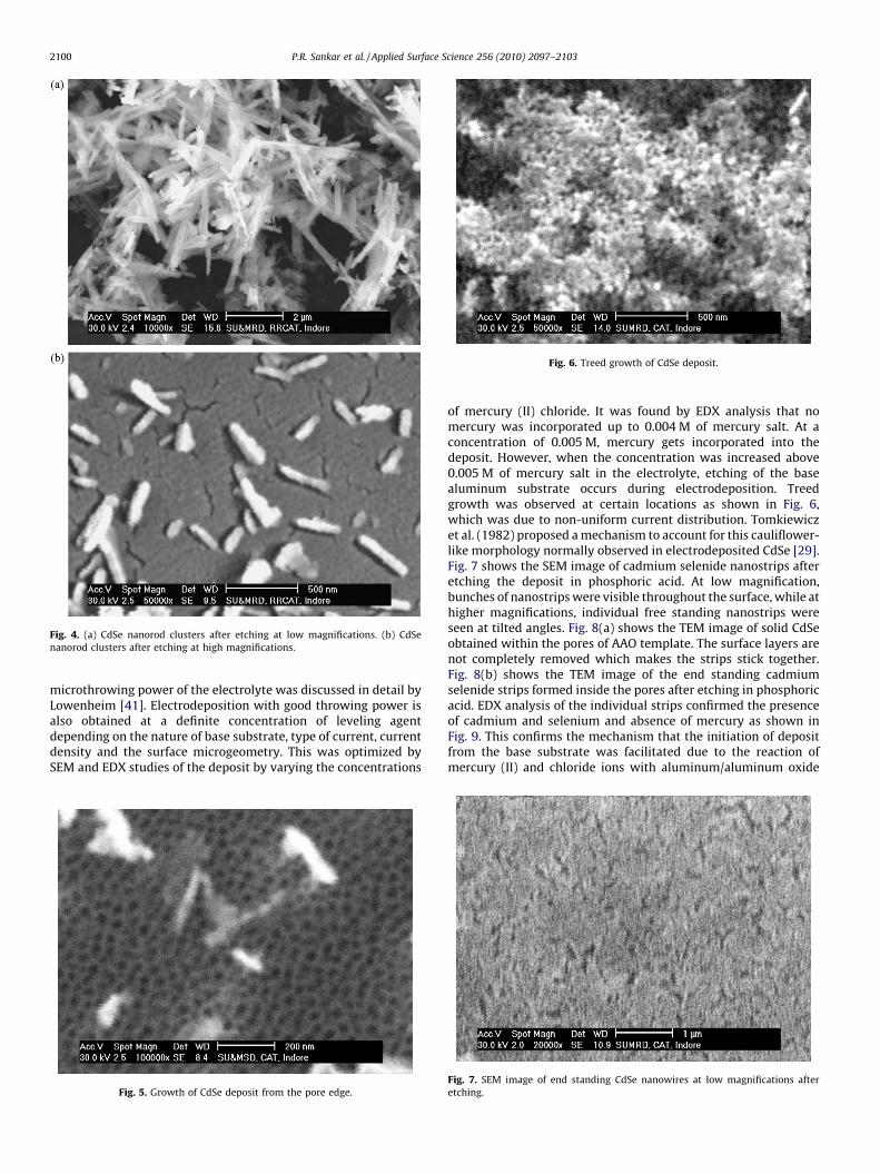
Fig. 4. (a) CdSe nanorod clusters after etching at low magnifications. (b) CdSe
nanorod clusters after etching at high magnifications.
Fig. 6. Treed growth of CdSe deposit.
P.R. Sankar et al. / Applied Surface Science 256 (2010) 2097–21032100
microthrowing power of the electrolyte was discussed in detail byLowenheim [41]. Electrodeposition with good throwing power isalso obtained at a definite concentration of leveling agentdepending on the nature of base substrate, type of current, currentdensity and the surface microgeometry. This was optimized bySEM and EDX studies of the deposit by varying the concentrations
Fig. 5. Growth of CdSe deposit from the pore edge.
of mercury (II) chloride. It was found by EDX analysis that nomercury was incorporated up to 0.004 M of mercury salt. At aconcentration of 0.005 M, mercury gets incorporated into thedeposit. However, when the concentration was increased above0.005 M of mercury salt in the electrolyte, etching of the basealuminum substrate occurs during electrodeposition. Treedgrowth was observed at certain locations as shown in Fig. 6,which was due to non-uniform current distribution. Tomkiewiczet al. (1982) proposed a mechanism to account for this cauliflower-like morphology normally observed in electrodeposited CdSe [29].Fig. 7 shows the SEM image of cadmium selenide nanostrips afteretching the deposit in phosphoric acid. At low magnification,bunches of nanostrips were visible throughout the surface, while athigher magnifications, individual free standing nanostrips wereseen at tilted angles. Fig. 8(a) shows the TEM image of solid CdSeobtained within the pores of AAO template. The surface layers arenot completely removed which makes the strips stick together.Fig. 8(b) shows the TEM image of the end standing cadmiumselenide strips formed inside the pores after etching in phosphoricacid. EDX analysis of the individual strips confirmed the presenceof cadmium and selenium and absence of mercury as shown inFig. 9. This confirms the mechanism that the initiation of depositfrom the base substrate was facilitated due to the reaction ofmercury (II) and chloride ions with aluminum/aluminum oxide
Fig. 7. SEM image of end standing CdSe nanowires at low magnifications after
etching.
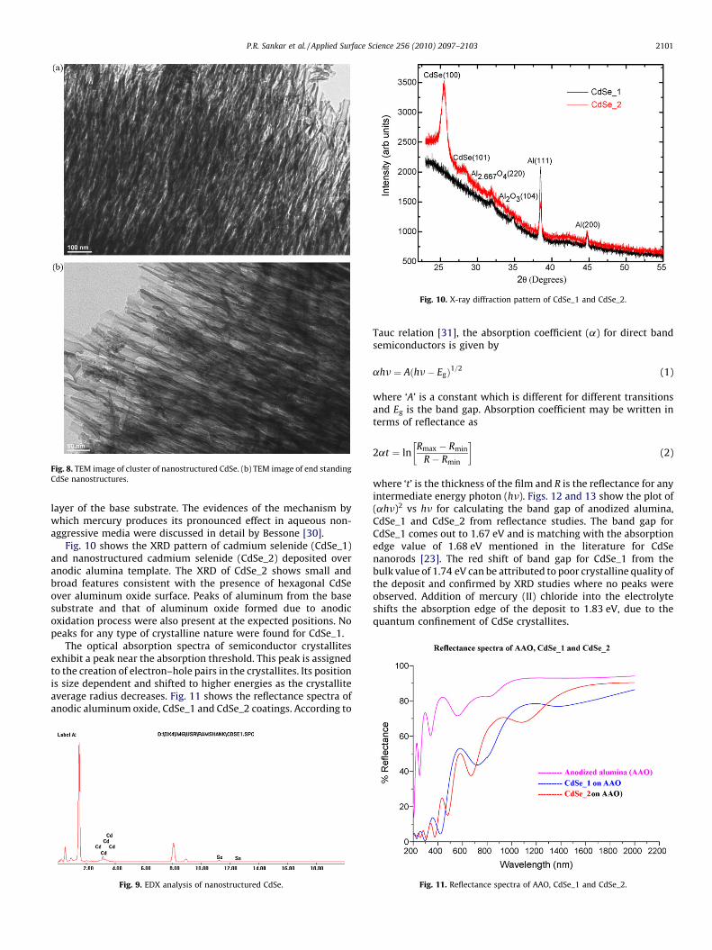
Fig. 8. TEM image of cluster of nanostructured CdSe. (b) TEM image of end standing
CdSe nanostructures.
Fig. 10. X-ray diffraction pattern of CdSe_1 and CdSe_2.
P.R. Sankar et al. / Applied Surface Science 256 (2010) 2097–2103 2101
layer of the base substrate. The evidences of the mechanism bywhich mercury produces its pronounced effect in aqueous non-aggressive media were discussed in detail by Bessone [30].
Fig. 10 shows the XRD pattern of cadmium selenide (CdSe_1)and nanostructured cadmium selenide (CdSe_2) deposited overanodic alumina template. The XRD of CdSe_2 shows small andbroad features consistent with the presence of hexagonal CdSeover aluminum oxide surface. Peaks of aluminum from the basesubstrate and that of aluminum oxide formed due to anodicoxidation process were also present at the expected positions. Nopeaks for any type of crystalline nature were found for CdSe_1.
The optical absorption spectra of semiconductor crystallitesexhibit a peak near the absorption threshold. This peak is assignedto the creation of electron–hole pairs in the crystallites. Its positionis size dependent and shifted to higher energies as the crystalliteaverage radius decreases. Fig. 11 shows the reflectance spectra ofanodic aluminum oxide, CdSe_1 and CdSe_2 coatings. According to
Fig. 9. EDX analysis of nanostructured CdSe.
Tauc relation [31], the absorption coefficient (a) for direct bandsemiconductors is given by
ahn ¼ Aðhn� EgÞ1=2 (1)
where ‘A’ is a constant which is different for different transitionsand Eg is the band gap. Absorption coefficient may be written interms of reflectance as
2at ¼ lnRmax � Rmin
R� Rmin
� �(2)
where ‘t’ is the thickness of the film and R is the reflectance for anyintermediate energy photon (hn). Figs. 12 and 13 show the plot of(ahn)2 vs hn for calculating the band gap of anodized alumina,CdSe_1 and CdSe_2 from reflectance studies. The band gap forCdSe_1 comes out to 1.67 eV and is matching with the absorptionedge value of 1.68 eV mentioned in the literature for CdSenanorods [23]. The red shift of band gap for CdSe_1 from thebulk value of 1.74 eV can be attributed to poor crystalline quality ofthe deposit and confirmed by XRD studies where no peaks wereobserved. Addition of mercury (II) chloride into the electrolyteshifts the absorption edge of the deposit to 1.83 eV, due to thequantum confinement of CdSe crystallites.
Fig. 11. Reflectance spectra of AAO, CdSe_1 and CdSe_2.
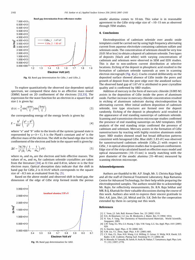
Fig. 12. Band gap determination for CdSe_1 and CdSe_2.
P.R. Sankar et al. / Applied Surface Science 256 (2010) 2097–21032102
To explore quantitatively the observed size dependent opticalspectrum, we compared these data to an effective mass model(EMM) based on 2D confinement of the electrons [32,33]. Theexpression for the wave function for an electron in a square box ofsize L is given by:
cðxÞ ¼ 2
Lsin
apx
L
� �sin
bpy
L
� �(3)
the corresponding energy of the energy levels is given by:
E ¼ h2
8m�a2 þ b2
L2
!(4)
where ‘‘a’’ and ‘‘b’’ refer to the levels of the system (ground state isrepresented by a = b = 1), h is the Plank’s constant and m* is theeffective mass of the electron. The shift in the band edge due to theconfinement of the electron and hole in the square well is given by:
DE ¼ 74:79
L2ðAÞ1
meþ 1
mh
� �ðeVÞ (5)
where me and mh are the electron and hole effective masses. Thevalues of me and mh for cadmium selenide crystallites are takenfrom the literature [34] as 0.13m and 0.41m, where m is the freeelectron mass. Optical absorption data indicate that the shift inband gap for CdSe_2 is 0.14 eV which corresponds to the squaresize of �8.5 nm as evaluated from Eq. (5).
Based on the above model and observed shift in band gap, thedimension of the edge of CdSe strip formed inside the porous
Fig. 13. Band gap determination for AAO.
anodic alumina comes to 10 nm. This value is in reasonableagreement to the CdSe strip edge size of �10–15 nm as observedthrough TEM studies.
4. Conclusions
Electrodeposition of cadmium selenide over anodic oxidetemplates could be carried out by using high frequency alternatingcurrent from aqueous electrolyte containing cadmium sulfate andselenium oxide. The concentration of selenium should be very low(0.01 M or less) to obtain a deposit of cadmium selenide. Two typesof deposits (black and white) with varying concentrations ofcadmium and selenium were observed in SEM and EDX studies.This is due to non-uniform current distribution at selectivelocations. Etching of the deposit in phosphoric acid resulted in theformation of cadmium selenide nanorods as seen in scanningelectron micrograph (Fig. 4(a)). Cracks created deliberately on thedeposited surface showed absence of CdSe inside the pores andgrowth of deposit from the pore edge over the anodized surface.The observed band gap of 1.67 eV is attributed to poor crystallinequality and is confirmed by XRD studies.
Addition of mercury in the form of mercuric chloride (0.005 M)assists in the deposition of CdSe inside the pores of aluminumoxide. Further increase in mercury chloride concentration resultedin etching of aluminum substrate during electrodeposition byalternating current. After initial uniform deposition of cadmiumselenide, tree type structures are formed over the depositrandomly. Etching of the deposit in phosphoric acid resulted inthe appearance of end standing nanostrips of cadmium selenide.Scanning and transmission electron microscope studies confirmedthe presence of end standing nanostrips on AAO templates. EDXanalysis of the end standing strips confirmed the presence ofcadmium and selenium. Mercury assists in the formation of CdSenanostructures by reacting with highly resistive aluminum oxidelayer. XRD studies showed small but broad diffraction patternsconsistent with hexagonal CdSe. Blue shift (1.83 eV) was observedfor nanostructured cadmium selenide (CdSe_2) with respect toCdSe_1 in optical absorption studies due to quantum confinement.Edge size of the strip calculated based on effective mass model andoptical measurements (10–15 nm) is nearly matching with thepore diameter of the anodic alumina (35–40 nm) measured byscanning electron microscope.
Acknowledgements
Authors are thankful to Mr. A.P. Singh, Mr. S. Christu Raja Singhand all the staff of Chemical Treatment Laboratory, Raja RamannaCentre for Advanced Technology, for their help while preparing theelectrodeposited samples. The authors would like to acknowledgeMr. Rajiv, for reflectivity measurements, Dr. B.N. Raja Sekhar andMR. B.Q. Khattak for their valuable discussions during the course ofthis work. Authors also wish to express their sincere gratitude toShri. A.K. Jain, Shri. J.K. Mittal and Dr. S.K. Deb for the cooperationextended by them in carrying out this work.
References
[1] C. Yoon, J.S. Suh, Bull. Korean Chem. Soc. 23 (2002) 1519.[2] D.A. Al-Mawlawi, C.Z. Liu, M. Moskovits, J. Mater. Res. 9 (1994) 1014.[3] H. Yan, P. Yang, The Chemistry of Nanostructured Materials, World Scientific,
Singapore, 2003.[4] L.W. Yang, X.L. Wu, G.S. Huang, T. Qiu, Y.M. Yang, G.G. Siu, Appl. Phys. A 81 (2005)
929.[5] A. Huezko, Appl. Phys. A 70 (2000) 365.[6] X.M. Liu, Y.C. Zhou, Appl. Phys. A 81 (2005) 685.[7] C.Y. Han, Z.L. Xiao, H.H. Wang, G.A. Willing, U. Geisar, U. Welp, W.K. Kwok, S.D.
Bader, G.W. Crabtree, Plating Surf. Finishing 91 (7) (2004) 40.[8] H. Masuda, H. Yamada, M. Satoh, H. Asoh, M. Nakao, T. Tamamura, Appl. Phys. Lett.
71 (19) (1997) 2770.
P.R. Sankar et al. / Applied Surface Science 256 (2010) 2097–2103 2103
[9] G. Zangari, D.N. Lambeth, IEEE Trans. Magn. 33 (5) (1997) 3010.[10] H. Masuda, K. Fakuda, Science 268 (1995) 1466.[11] O. Jessensky, F. Muller, U. Gosele, Appl. Phys. Lett. 72 (10) (1998) 1173.[12] T. Ohgai, L. Gravier, X. Hoffer, M. Lindeberg, K. Hjort, R. Spohr, J.-Ph. Ansermet, J.
Phys. D: Appl. Phys. 36 (2003) 3109.[13] T. Gao, G.W. Meng, J. Zhang, C.H. Liang, J.C. Fan, L.D. Zhang, Appl. Phys. A 73 (2001)
251.[14] X. Bao, F. Li, R.M. Metzger, J. Appl. Phys. 79 (1996) 4866.[15] M.P. Zach, K.H. Ng, R.M. Penner, Science 290 (2000) 2120.[16] P.V. Kamat, Electrochemistry of Nanomaterials, Wiley–VCH, Weinheim, 2001
(Chapter 8).[17] P.P. Hankare, V.M. Bhuse, K.M. Garadkar, S.D. Delekar, I.S. Mulia, Mater. Chem.
Phys. 82 (2003) 711.[18] H. Yan, P. Yang, The Chemistry of Nanostructured Materials, World Scientific,
Singapore, 2003 (Chapter 7).[19] H. Weller, Adv. Mater. 5 (1993) 88.[20] M. Anpo, H. Yamashita, Heterogenous Photocatalysis, Wiley, England, 1997.[21] M.C. Neves, J. Soares, R. Hempelmann, T. Monteiro, T. Trindade, J. Cryst. Growth
279 (2005) 433.[22] K.N. Shreekanthan, B.V. Rajendra, V.B. Kasturi, G.K. Shivakumar, Cryst. Res.
Technol. 38 (2003) 30.[23] Q. Peng, Y. Dong, Z. Deng, Y. Li, Inorg. Chem. 41 (2002) 5249.[24] C.N.R. Rao, A. Govindaraj, Nanotubes and Nanowires, RSC Publishing, Cambridge,
UK, 2005 (Chapter 3).[25] D.J. Pena, J.K.N. Mbindyo, A.J. Carado, T.E. Mallouk, C.D. Keating, B. Razavi, T.S.
Mayer, J. Phys. Chem. B 106 (2002) 7458.
[26] D. Xu, D. Chen, Y. Xu, X. Shi, G. Guo, L. Gui, Y. Tang, Pure. Appl. Chem. 72 (2000)127.
[27] D. Xu, X. Shi, G. Guo, L. Gui, Y. Tang, J. Phys. Chem. B 104 (2000) 5061.[28] D. Routkevitch, et al. J. Phys. Chem. 100 (1996) 14037.[29] Micha Tomkiewicz, Ivy Ling, S. William, Parsons, J. Electrochem. Society 129
(1982) 2016.[30] J.B. Bessone, Corros. Sci. 48 (12) (2006) 4243.[31] S.K. Sharma, L. Kumar, S. Kumar, T.P. Sharma, Chalcogenide Lett. 5 (4) (2008)
73.[32] L.D. Landau, E.M. Lifshitz, Quantum Mechanics, 3rd edition, Butterworth Hei-
memann Publications, Oxford, 1977, p. 63.[33] M.S. Gudiksen, J. Wang, C.M. Lieber, J. Phys. Chem. B 106 (2002) 4036.[34] P.E. Lippens, M. Lannoo, Phys. Rev. B 41 (9) (1990) 6079.[35] G. Riveros, J. Vasquez, H. Gomez, T. Makoarova, D. Silva, R.E. Marotti, E.A.
Dalchiele, Appl. Phys. A 90 (2008) 423.[36] X.S. Peng, J. Zhang, X.F. Wang, Y.W. Wang, L.X. Zhao, G.W. Meng, L.D. Zhang, Chem.
Phys. Lett. 343 (2001) 470.[37] L.K. The, V. Furin, A. Martucci, M. Guglielmi, C.C. Wong, F. Romanato, Thin Solid
Films 515 (2007) 5787.[38] D. Routkevitch, A.A. Tager, J. Haruyama, D. Almawlawi, M. Moskovits, J.M. Xu, IEEE
Trans. Electron Devices 43 (10) (1996) 1646.[39] J Sherman, Materials, 2007 REU Research accomplishments.[40] J. Sarkar, G. Gopal Khan, A. Basumallick, Bull. Bull. Mater. Sci. 30 (June (3)) (2007)
271–290.[41] F.A. Lowenheim, Modern Electroplating, A Wiley–Interscience Publication, New
York, 1973 (Chapter 1).