Self-heating of silicon microwires: Crystallization and thermoelectric effects
11
INVITED FEATURE PAPER Self-heating of silicon microwires: Crystallization and thermoelectric effects Gokhan Bakan a) , Niaz Khan, Adam Cywar, Kadir Cil, Mustafa Akbulut, Ali Gokirmak, and Helena Silva b) Department of Electrical and Computer Engineering, University of Connecticut, Storrs, Connecticut 06269 (Received 24 September 2010; accepted 18 January 2011) We describe experiments on self-heating and melting of nanocrystalline silicon microwires using single high-amplitude microsecond voltage pulses, which result in growth of large single-crystal domains upon resolidification. Extremely high current densities (.20 MA/cm 2 ) and consequent high temperatures (1700 K) and temperature gradients (1 K/nm) along the microwires give rise to strong thermoelectric effects. The thermoelectric effects are characterized through capture and analysis of light emission from the self-heated wires biased with lower magnitude direct current/ alternating current voltages. The hottest spot on the wires consistently appears closer to the lower potential end for n-type microwires and to the higher potential end for p-type microwires. The experimental light emission profiles are used to verify the mathematical models and material parameters used for the simulations. Good agreement between experimental and simulated profiles indicates that these models can be used to predict and design optimum geometry and bias conditions for current-induced crystallization of microstructures. I. INTRODUCTION Polycrystalline silicon (poly-Si), amorphous silicon (a- Si), and nanocrystalline silicon (nc-Si) are commonly used for large-area electronics such as flat panel dis- plays, 1 x-ray imaging arrays, 2 and solar cells. Currently, a-Si is used in Si thin-film transistors for large-area electronics 1 due to its uniformity and low-temperature pro- cessing, despite its relatively low electrical carrier mobil- ity. 3 There is a growing demand for displays and sensors on larger areas, using flexible and shatter-proof substrates like plastics, that can operate at higher speeds and sensi- tivities. Large areas require uniformity; flexible substrates require low-temperature processing; and higher speed and sensitivity require use of crystalline material instead of amorphous material. Cost-effective techniques to achieve single-crystal Si on arbitrary substrates will also enable significant technological advancements, such as integra- tion of high performance circuitry with displays or sensor arrays as complete systems. The interest in achieving high-speed circuitry for large- area electronics has motivated studies on crystal growth on glass and plastics, 4 transfer of crystalline structures onto glass and plastic substrates, and crystallization of low temperature-deposited Si. 1,2,5 Vapor–liquid–solid growth 4 of Si nanowires leads to single-crystal structures, 6 which are compatible with glass and potentially with plastic substrates. The remaining challenges for this approach are related to orientation and placement control. Transfer of single-crystal islands or large areas can be achieved with silicon-on-insulator (SOI) wafers and using layer transfer techniques, which allow good control over orientation and placement. This is achieved by bonding a handle wafer to the top Si layer, etching of the underlying oxide, bonding of the thin Si layer to the host substrate, and detaching from the handle wafer. This approach, requiring SOI wafers, is cost prohibitive. 7 Crystallization of low temperature-deposited a-Si films is a promising approach that has been studied in the past decades. This requires thermal processing of a-Si. High temperature annealing of a-Si films typically results in polycrystalline films. However, it has been reported that patterning the films to form microstructures with widths smaller than 250 nm can result in the growth of single crystal along the length with preferred crystal orientation. Metal-induced crystallization 8,9 reduces the required tem- perature significantly, making it more compatible with low temperature substrates, but there are some concerns re- garding the metal contamination in the crystallized films. 10 Local heating techniques, where the energy required for heating is directly delivered to the film or the patterned structures, allow the substrate to remain at room tempera- ture. These techniques include sequential lateral solidifica- tion using an excimer laser, 11,12 rapid melting and growth from melt using self-heating, 13 or microfabricated heaters atop the structures. 14 Some of the laser annealing techniques, such as sequential lateral crystallization, are currently in industrial use. Address all correspondence to these authors. a) e-mail: [email protected] b) e-mail: [email protected] This paper has been selected as an Invited Feature Paper. DOI: 10.1557/jmr.2011.32 J. Mater. Res., Vol. 26, No. 9, May 14, 2011 Ó Materials Research Society 2011 1061
-
Upload
independent -
Category
Documents
-
view
1 -
download
0
Transcript of Self-heating of silicon microwires: Crystallization and thermoelectric effects
INVITED FEATURE PAPER
Self-heating of silicon microwires: Crystallization and thermoelectriceffects
Gokhan Bakana), Niaz Khan, AdamCywar, Kadir Cil, Mustafa Akbulut, Ali Gokirmak, andHelena Silvab)
Department of Electrical and Computer Engineering, University of Connecticut, Storrs, Connecticut 06269
(Received 24 September 2010; accepted 18 January 2011)
We describe experiments on self-heating and melting of nanocrystalline silicon microwires usingsingle high-amplitude microsecond voltage pulses, which result in growth of large single-crystaldomains upon resolidification. Extremely high current densities (.20 MA/cm2) and consequenthigh temperatures (1700 K) and temperature gradients (1 K/nm) along the microwires give rise tostrong thermoelectric effects. The thermoelectric effects are characterized through capture andanalysis of light emission from the self-heated wires biased with lower magnitude direct current/alternating current voltages. The hottest spot on the wires consistently appears closer to the lowerpotential end for n-type microwires and to the higher potential end for p-type microwires. Theexperimental light emission profiles are used to verify the mathematical models and materialparameters used for the simulations. Good agreement between experimental and simulated profilesindicates that these models can be used to predict and design optimum geometry and bias conditionsfor current-induced crystallization of microstructures.
I. INTRODUCTION
Polycrystalline silicon (poly-Si), amorphous silicon (a-Si), and nanocrystalline silicon (nc-Si) are commonlyused for large-area electronics such as flat panel dis-plays,1 x-ray imaging arrays,2 and solar cells. Currently,a-Si is used in Si thin-film transistors for large-areaelectronics1 due to its uniformity and low-temperature pro-cessing, despite its relatively low electrical carrier mobil-ity.3 There is a growing demand for displays and sensorson larger areas, using flexible and shatter-proof substrateslike plastics, that can operate at higher speeds and sensi-tivities. Large areas require uniformity; flexible substratesrequire low-temperature processing; and higher speed andsensitivity require use of crystalline material instead ofamorphous material. Cost-effective techniques to achievesingle-crystal Si on arbitrary substrates will also enablesignificant technological advancements, such as integra-tion of high performance circuitry with displays or sensorarrays as complete systems.
The interest in achieving high-speed circuitry for large-area electronics has motivated studies on crystal growthon glass and plastics,4 transfer of crystalline structuresonto glass and plastic substrates, and crystallization of lowtemperature-deposited Si.1,2,5
Vapor–liquid–solid growth4 of Si nanowires leads tosingle-crystal structures,6 which are compatible with glass
and potentially with plastic substrates. The remainingchallenges for this approach are related to orientationand placement control.Transfer of single-crystal islands or large areas can be
achieved with silicon-on-insulator (SOI) wafers and usinglayer transfer techniques, which allow good control overorientation and placement. This is achieved by bondinga handle wafer to the top Si layer, etching of theunderlying oxide, bonding of the thin Si layer to the hostsubstrate, and detaching from the handle wafer. Thisapproach, requiring SOI wafers, is cost prohibitive.7
Crystallization of low temperature-deposited a-Si filmsis a promising approach that has been studied in the pastdecades. This requires thermal processing of a-Si. Hightemperature annealing of a-Si films typically results inpolycrystalline films. However, it has been reported thatpatterning the films to form microstructures with widthssmaller than 250 nm can result in the growth of singlecrystal along the length with preferred crystal orientation.Metal-induced crystallization8,9 reduces the required tem-perature significantly, making it more compatible with lowtemperature substrates, but there are some concerns re-garding themetal contamination in the crystallized films.10
Local heating techniques, where the energy requiredfor heating is directly delivered to the film or the patternedstructures, allow the substrate to remain at room tempera-ture. These techniques include sequential lateral solidifica-tion using an excimer laser,11,12 rapid melting and growthfrom melt using self-heating,13 or microfabricated heatersatop the structures.14 Some of the laser annealing techniques,such as sequential lateral crystallization, are currently inindustrial use.
Address all correspondence to these authors.a)e-mail: [email protected])e-mail: [email protected] paper has been selected as an Invited Feature Paper.DOI: 10.1557/jmr.2011.32
J. Mater. Res., Vol. 26, No. 9, May 14, 2011 �Materials Research Society 2011 1061

The approach described in this article is crystallizationof nc-Si microwires through single microsecond voltagepulses, leading to self-heating, melting, and growth frommelt in a very short time (1 ls). The short duration localheating of the structures to be crystallized makes thisapproach compatible with low temperature substrates.Real-time current–voltage measurements can be madeon these structures during the crystallization process,which can help in understanding the mechanisms in-volved. The extreme thermal gradients (1 K/nm) and theshort time scales involved in these experiments are similarto those in pulse laser annealing. The main differences inthis case are due to formation of molten filaments in thecurrent path and thermoelectric effects, which appear to bevery strong under the extremely high electric currentdensities (.20 MA/cm2) during the voltage pulse. Here,we give an overview of our experimental observations onmelting, growth from melt and thermoelectric effects, andcomputational studies on heating and cooling of the wires,including the role of thermoelectric effects.
II. EXPERIMENTAL
A. Fabrication
The microwires are patterned on n- and p-type nc-Sifilms deposited on oxidized single-crystal Si wafers(500-nm SiO2) in a low pressure chemical vapor de-position system at 580 or 600 °Cwith phosphorous dopingor at 560 °C with boron doping ([P], [B] . 1020 cm�3).The room temperature resistivities of the n- and p-typefilms are 22.956 0.29 mX�cm and 12.886 0.26 mX�cm,respectively. Some of the microwires are suspended byetching the underlying oxide using buffered oxide etch.Dimensions of the wires range from 0.5 to 25 lm in lengthand from 100 nm to 1 lm inwidth.Metal extensions (Ti/Nior Ti/Al stacks) are deposited to form ohmic contacts to theSi pads. The fabrication process is shown in Fig. 1. Figure 2shows scanning electron microscope (SEM) images of twoas-fabricated microwires.
B. Microsecond voltage pulse crystallization
The experiments are conducted using a semiconductorprobe station, a parameter analyzer, a pulse generator
unit, and an oscilloscope. The setup is configured as seenin Fig. 3(a) for experiments on crystallization through self-heating. The I–V characteristics of the microwires aremeasured before and after the voltage pulses using theparameter analyzer. The applied voltage (VPulse) andvoltage across the 50 X termination (VG) are measuredby the oscilloscope during the pulse. Current through thewire is calculated as the resistive current through the 50 Xtermination (VG/50) because the capacitive current iscalculated to be less than 1% of the resistive current.Tungsten needles are used to probe the metal contacts orthe Si contact regions of microwires without metalextensions.15
A single high-amplitude voltage pulse applied to a wireresults in a characteristic nonlinear increase in currentthrough the wire because of self-heating during thevoltage pulse [Fig. 4(i)]. Figure 4 shows that the peakcurrent levels increase with wire width and all other thanthe narrowest structure break during the voltage pulse ascan be seen in the sudden drop in the current during thevoltage pulse. I–t plots show stable plateaus [Fig. 4(i)]with corresponding peak current densities in the order of10 MA/cm2. The SEM images of these structures after thepulse suggest that the wires melt before breaking, andmelting is more severe for wider structures [Figs. 4(g) and4(h)]. Narrower microwires show two smooth, crystallizedwire segments at the two ends [Figs. 4(b)–4(f)]. Thenarrowest microwire shows only the formation of narrowfilaments on the Si pads and surface modification on thewire [Fig. 4(a)].
The melting of the wires is verified by extracting thewire resistivity during the pulse when I–t plots showa plateau. This is achieved by calculating the resistance(VPulse/IWire) of a number of structures with different widthsand lengths. The solid-state microwire lengths and thick-nesses are known accurately; however, widths (W ) aresignificantly smaller than the design widths (WD) due tooverexposure of photoresist duringmaskmaking and patterntransfer processes. The actual wire widths are calculatedfrom electrical measurements performed on an array ofdevices with varyingwidths and lengths. Linear fits aremadeto room temperature resistance versus length for differentwidths [Fig. 5(a)].The slopes from those fits plotted asa function of design width are used to extract the difference
FIG. 1. Device fabrication schematics: (a) silicon dioxide (SiO2) growth and nanocrystalline silicon (nc-Si) deposition; (b) patterning of the nc-Sifilm; (c) forming of metal extensions.
G. Bakan et al.: Self-heating of silicon microwires: Crystallization and thermoelectric effects
J. Mater. Res., Vol. 26, No. 9, May 14, 20111062

between design and actual widths (DW) [Fig. 5(b)]. Theactual wire dimensions and the resistance (VPulse/IWire) ofthe wires at the plateau of the I–t plots are used to calculatethe resistivity,15,19 yielding 73.3 6 3.9 lX�cm. This valueis in good agreement with previous reports on liquid Siresistivity of 83 lΩ�cm byGlazov et al.,16 75.26 0.6 lΩ�cmby Schnyders and Van Zytveld,17 and 72 lΩ�cm by Sasakiet al.18 Liquid Si at melting temperature is reported to be10% denser than Si at solid phase at room temperature.16
Liquid Si resistivity is extracted to be 66.0 6 3.5 l�cm,accounting for 10% volume reduction in liquid phase fromthese microsecond voltage pulse experiments.
The resistance of Si pads, the y-intercept in the resistanceversus length plots of wires in liquid state, is on the order of50 X, suggesting highly conductive continuous liquid Sipaths between the twometal contacts [Fig. 5(c)]. Themoltenand resolidified filaments, indicating the percolation paths20
between the metal contacts and the wire, are visible in theSEM images (Fig. 4). Faster increase in the temperature ofthe least resistive percolation path and negative temperaturecoefficient of the nc-Si films result in a positive feedback,leading to an increase in both current density and temperatureon this path as most of the current collapses on a narrowfilament on the Si pads. Themoltenfilaments resolidify upontermination of the voltage pulse. The filamentation processtakes place in less than 1 ls for the microwires seen in Fig. 4for the given voltage pulse conditions.
Melting of the wires requires less current, and themechanical stress induced by the substrate is eliminated ifthe wires are suspended by removing some of theunderlying oxide. The heat loss from the suspended
FIG. 2. Scanning electron microscope (SEM) images of as-fabricated(a) suspended microwire and (b) microwire on oxide with metalextensions. The parts of the structure that are released from theunderlying oxide appear as lighter color.
FIG. 3. (a) Schematic of the experimental setup. RMetal and RSi areresistances of metal extension and total Si resistance (contact pad andwire), respectively. C is the coaxial cable capacitance (100 pF). (b)Example of voltage pulse with 16 V amplitude and 1 ls duration.
FIG. 4. (a)–(h) SEM images of 5.5-lm long, p-type microwires after20 V, 1 ls pulses. Wide microwires show breaking and crystallizedsegments or Si accumulation on Si pads under the same pulse condition.(i) I–t plots of the microwires show two transitions and a flat regionbefore the wires break.
G. Bakan et al.: Self-heating of silicon microwires: Crystallization and thermoelectric effects
J. Mater. Res., Vol. 26, No. 9, May 14, 2011 1063

wires is predominantly to the contact regions at the twoends. The as-fabricated suspended microwires, wide andthin with uniform nanocrystalline texture as seen underSEM [Fig. 6(a)], acquire a cylindrical shape with smoothsurfaces (due to surface tension) and a lump in the middle[Fig. 6(b)] upon melting and resolidification. The as-fabricated structures have compressive stress, seen assagging of the structures after the release [Fig. 6(a)]. Therecrystallized wires are stretched between the contactpads, indicating a tensile stress. The resolidification pro-cess starts from the Si pads and move toward the middle ofthe microwire. Some of the liquid Si cannot fit in themiddle as the two solid–liquid fronts meet because Si
expands as it solidifies. Excess Si is ejected and formsa lump after resolidification [Fig. 6(b)]. The microwiresthat experience longer duration pulses show tapering andbreaking [Fig. 6(c)] through Si migration toward the Sipads. Strong thermal gradient along the suspended micro-wires, owing to low heat loss to the substrate, is expectedto suppress nucleation along the wire and consequentlylimits the number of grains to two, one starting from eachend. Microwires on oxide, experiencing smaller thermalgradients during cooling, may resolidify to formmore thantwo grains along the wire [Fig. 4(a)].
The conductance of the microwires is enhanced afterthe voltage pulse. Figure 6(b) shows a 3.5-lm-long
FIG. 5. (a) Room temperature resistance of microwires with different widths as a function of length from one test site. The y-intercept corresponds tothe Si pad resistance, which is expected to be approximately the same for all microwires. (b) Reciprocal of a as a function of design width, obtainedfrom the linear fits in (a). The x-intercept corresponds to the difference between design and actual widths. (c) Resistance of the liquid path for differentwidths as a function of length as extracted from the flat regions of the I–t plots. (d) Calculated liquid Si resistivity from three different test sites. Dashedlines indicate previous liquid Si resistivity reports: (i) Ref. 16 (ii) Ref. 17, and (iii) Ref. 18.
FIG. 6. (a) An as-fabricated, n-type, suspended microwire and two microwires after (b) 40 V, 1 ls and (c) 40 V, 2 ls pulse. Resistance of the wire in(b) decreased significantly after the pulse.
G. Bakan et al.: Self-heating of silicon microwires: Crystallization and thermoelectric effects
J. Mater. Res., Vol. 26, No. 9, May 14, 20111064

microwire with prepulse total resistance of 56.7 kX. Thetotal resistance (RSi) consists of the microwire (10 kX) andSi pad resistances (40 kX). After the voltage pulse, thetotal resistance of the microwire in Fig. 6(b) was measuredas 22.2 kΩ, which is smaller than the prepulse Si padresistance. Low postpulse resistance is attributed toconductance enhancement in both the microwires andthe contact regions, even though the changes in the contactregions are not observable under SEM in this case.Resistivity of the pulsed, unbroken microwires is reducedby a factor of up to10�,21 indicating crystal growth ratherthan solidification in amorphous form.
Crystallization is also verified with transmission elec-tron microscope (TEM) studies on a long (20 lm),suspended, p-type microwire, which experienced a singlevoltage pulse. A short segment of long microwire touchesthe underlying oxide after the release of the wire due tocompressive stress as observed under SEM before thepulse [Fig. 7(a)]. After the pulse, the microwires showsmooth surfaces with multiple lumps along the length[Figs. 7(b) and 7(c)]. This wire was cut and placed ona TEM sample holder using a focused ion beam system.Figure 8 shows a bright field TEM image and electrondiffraction analysis of a section of the microwire seen inFig. 7, which shows existence of a single crystal in theimaged area.
C. Capture and analysis of light emission from themicrowires under long duration biases
The microsecond pulsing of the microwires results invery high current densities (.20 MA/cm2). The peaktemperature on the wire reaches the melting temperature ofSi (1690 K), while the contact pads remain at roomtemperature, leading to thermal gradients on the order of1 K/nm. Thermoelectric effects are expected to be very
significant at such current densities and thermal gra-dients.22,23 The transient effects in the short time scalesinvolved in melting and crystallization in these experi-ments are difficult to probe. However, it is possible to gainsome information about the steady-state temperature pro-file and the thermoelectric effects from the light emittedfrom the wire as it is heated up to 1000 K and beyond. Thisallows for verification of the high temperature materials’parameters and models used for the computational studies.
The first optical observation of thermoelectric effectsin a single material system (Thomson effect) was reportedby Mastrangelo et al.24 The authors observed that the peaklight intensity (hottest spot) on p-type poly-Si microlampswas shifted from the center toward the higher potential end(V+). Englander et al.25 observed a similar asymmetriclight emission profile shifted toward the lower potentialterminal in n-type poly-Si microheaters. Jungen et al.26
also reported a shift toward the lower potential end for self-heated, n-type poly-Si, microbridges.
Thermoelectric effects (thermoelectricity) is due to thecoupling of electronic and heat transport through heattransfer by charge carriers. Direct electrical–thermalenergy conversion for power generation, solid-state cool-ing,22,23 and characterization of semiconductor materials27
are the most common applications of thermoelectricity.Thermoelectricity can be observed as an open-circuitvoltage across a temperature difference in a circuit oftwo different materials (Seebeck effect), heating or cool-ing at a current-passing junction between two differentmaterials (Peltier effect), and heating or cooling alonga current-carrying homogeneous material under a temper-ature gradient (Thomson effect). The Seebeck voltagepolarity and heating versus cooling for Peltier and Thom-son effects depend on temperature-dependent thermoelec-tric properties of the material and directions of temperaturegradient and electric current. The three thermoelectriceffects are characterized by the Seebeck (S), Peltier (P),and Thomson (b) coefficients, which are interrelated bythe fundamental Kelvin relationships23:
FIG. 7. SEM image of a (a) 25-lm long, suspended, p-type microwire,(b) 20-lm long, suspended, p-type microwire after a 25 V, 1 ls pulsewith current direction during the pulse as indicated. (c) Closeup image ofleft end of the microwire. (d) I–t plot of the microwire during pulse,showing onset of melting as a sudden increase in current.
FIG. 8. Bright field transmission electron microscope image of a sec-tion of a 20-lm long crystallized microwire and corresponding electrondiffraction pattern (inset).
G. Bakan et al.: Self-heating of silicon microwires: Crystallization and thermoelectric effects
J. Mater. Res., Vol. 26, No. 9, May 14, 2011 1065

P5 ST ; ð1Þ
b5TdS
dT: ð2Þ
Thomson effect results in skewing of temperatureprofiles and is typically very small in macroscopicstructures; however, it is significant in self-heatedsmall-scale structures such as microlamps24 and micro-heaters25,26 as mentioned earlier, as well as phase-changememory (PCM) elements,28 owing to the large currentdensities and temperature gradients. In all these cases ofself-heating at high temperatures, the hottest spot along thestructures appears closer to the lower potential end (V�)for n-type structures and closer to the higher potential end(V+) for p-type structures, in agreement with expectedhigh-temperature positive Thomson coefficient for n-type(b . 0) and high–temperature negative Thomson co-efficient for p-type (b , 0) materials (Fig. 12).
Castro et al.28 have calculated a Thomson coefficient of�100 lV/K for SbTe above room temperature using ananalytical solution for the hottest spot location and in-dicated that a 5% reduction in RESET current wasobtained in asymmetric PCM structures due to Thomsoneffect. However, changes in the material during theheating process can contribute to the asymmetry in thetemperature profile, and hence, the observed asymmetriesmay be larger than what is due to the pure contribution ofthermoelectric effects.
In our experiments, we have recorded videos of lightemission from self-heated nc-Si microwires using a highmagnification optical setup and a commercial high-definition (full HD) camcorder at 30 frames per second.The wires self-heated to sufficiently high temperatures(T. 800 °C25) emit light in the visible range. The speed ofthe measurement is limited by the sensitivity and the framerate of the camera. Hence, the light emission from thewires was observed with slow voltage sweeps and alter-nating current (AC) signals at 1 Hz frequency. The lightintensity profiles along the microwires and shift in thebrightest (hottest) spot are extracted from the videos usingMATLAB.
As the current increases, the hottest spot on themicrowires always shifts toward the lower potential endfor n-type microwires and to the higher potential end forp-type microwires, in agreement with the previousreports.24–26 Figure 9 shows two sets of video framesand corresponding light intensity profiles along 4-lm-long, n- and p-type microwires as current increases. Thehottest spot is shifted 1.5 lm away from the center of the n-type microwire (37% of the length) and by 1.15 lm from
the center of the p-type microwire (30% of the length) forthe highest current achieved (.1 MA/cm2). These resultsare higher than those of previous reports of 5% on p-type,poly-Si microlamps and;20% on n-type, poly-Si heaters.We attribute the larger shifts in our experiments on nc-Simicrowires to the larger current densities and local de-formation of the microwires where the hottest spot wasobserved (Fig. 10). This local deformation suggests in-creased resistance at this location, leading to increasedlocal heating and a positive feedback for the shift in thelocation of the hottest spot.
FIG. 9. Two sets of video frames showing glow of (a) an n-type and (b)a p-type microwire as current through the microwires increases asindicated. Electrical bias conditions are shown on the top frames.Microwires’ dimensions (L, W, t) are (4, 0.41, 0.08) lm and (4, 0.42,0.12) lm for the n- and p-type microwires, respectively. Evolution ofglow intensity for the (c) n- and (d) p-type microwires. Wire centers arelocated at x 5 0. Dashed lines indicate ends of the microwires. Curvesare smoothened with 5-point adjacent averaging filter.
FIG. 10. SEM image of a p-type microwire after a slow voltage sweep,with current direction as indicated. The higher potential end of themicrowire, which coincides with the hottest region as observedoptically, shows significant modification and fractures.
G. Bakan et al.: Self-heating of silicon microwires: Crystallization and thermoelectric effects
J. Mater. Res., Vol. 26, No. 9, May 14, 20111066

The effect of changes in the material can be identifiedand eliminated to some degree by alternating the currentdirection using an AC signal. Figures 11(a) and 11(b)
show glowing of a 2.5-lm-long, suspended, n-type micro-wire during positive and negative cycles of an AC signalgenerated by a parameter analyzer. The hottest spot on themicrowire alternates position as the current directionchanges, confirming that the shift of the hottest spot isnot caused by any asymmetric geometrical or thermalboundaries but by thermoelectric effects. Figure 11(c)shows current through the microwire and the shift in thehottest spot location as a function of time. The shift in thehottest spot for either cycle of the AC signal is ;250 nm(10% of the length). The shift in the hottest spot for thenegative cycle gradually increases over time, showinga memory effect. Similar behavior is observed on otherwires when they are biased with opposite polarity of theprevious bias. Suspended microwires exhibit smallerasymmetries compared to unsuspended ones because theyreach glowing temperatures for lower current levels;hence, they show weaker thermoelectric effects.
D. Numerical modeling
The experimental results are complemented by finiteelement analysis of a 2.5-lm-long, suspended, n-typemicrowire using COMSOL Multiphysics software,29 in-cluding the thermoelectric effects, using the parametersavailable in the literature. The thermoelectric effects areincluded in both current continuity and heat transferequations30:
FIG. 12. Experimental Seebeck coefficient of Si as a function of temperature from the literature. Crystallinity, dopant type, and doping level orresistivity of the samples are indicated in the legend. nb-Si is used for nanobulk Si. aRef. 34, bRef. 32, cRef. 33, dRef. 35, and eRef. 36.
FIG. 11. A 2.5-lm-long, suspended, n-type microwire during the(a) positive and (b) negative cycle of an applied square wave with0.95 mA amplitude. Current levels and directions are as indicated. Wirecenter is located at x5 0. (c) Current (I) through the microwire and shift(Dx) in the hottest spot location as a function of time.
G. Bakan et al.: Self-heating of silicon microwires: Crystallization and thermoelectric effects
J. Mater. Res., Vol. 26, No. 9, May 14, 2011 1067

=:J5 � =:=V þ S=T
q
� �5 0 ; ð3Þ
dSiCP
dT
dt� =:ðk=TÞ5qJ:J � TJ:=S ; ð4Þ
where dSi is the density, CP is the specific heat, k is thethermal conductivity, q is the electrical resistivity, and S isthe Seebeck coefficient. The thermoelectric term (�TJ=S)in Eq. (4) reduces to the Thomson heat for homogeneousstructures �T ðdS
dTÞJ=T� �
.The resistivity of the microwire is modeled as an
exponentially decaying function from its room tempera-ture value of 23 mX�cm to the melting temperature valueof 3 mX�cm, following the trend of the measured re-sistivity in the 300–650 K range (q 5 3.2 + 195.5 e�T/142
mX�cm).18 Temperature-dependent thermal conductivityand Seebeck coefficient are not yet characterized for theheavily doped nc-Si used for the fabrication of the wires,nor are there any thermal conductivity or Seebeck co-efficient data available in the literature on nc-Si, to the bestof our knowledge. Hence, an inverse polynomial extrap-olation function given in Ref. 31, fitting the experimentalthermal conductivity of heavily doped poly-Si in the 300–800 K range, is used. Similarly, Seebeck coefficient ofheavily doped poly-Si ([P] ~ 1020 cm�3) is used at lowtemperature range (150–450 K)32 and Seebeck coefficientof poly-Si with [P] 5 6 � 1017 cm�3 is used at hightemperature range (700–1350 K) for modeling.33 TheSeebeck coefficient in the 450–700 K range is extrapolatedlinearly from these two poly-Si datasets, which intersect at800 K, and it is also linearly extrapolated in the rangebetween 1350 and 1690 K using the high temperature data(Fig. 12). Density and specific heat of c-Si are close tothose of poly-Si and a-Si37 and change only slightly withtemperature; therefore, constant (room temperature) c-Sivalues29 are used. The room temperature values of themodeling parameters of nc-Si, SiO2, and c-Si layers areshown in Table I. Figure 13 shows the three-dimensionalstructure used for the modeling of the microwire and theelectrical and thermal boundaries. A 5.8 V, 1 ls voltagepulse or square wave (AC) with increasing amplitude is
applied across the wire. The current continuity and heattransfer equations including thermoelectric effects aresolved self-consistently [Eqs. (3) and (4)]. The modelingof pulsed wires is also performed without thermoelectriceffects for comparison.
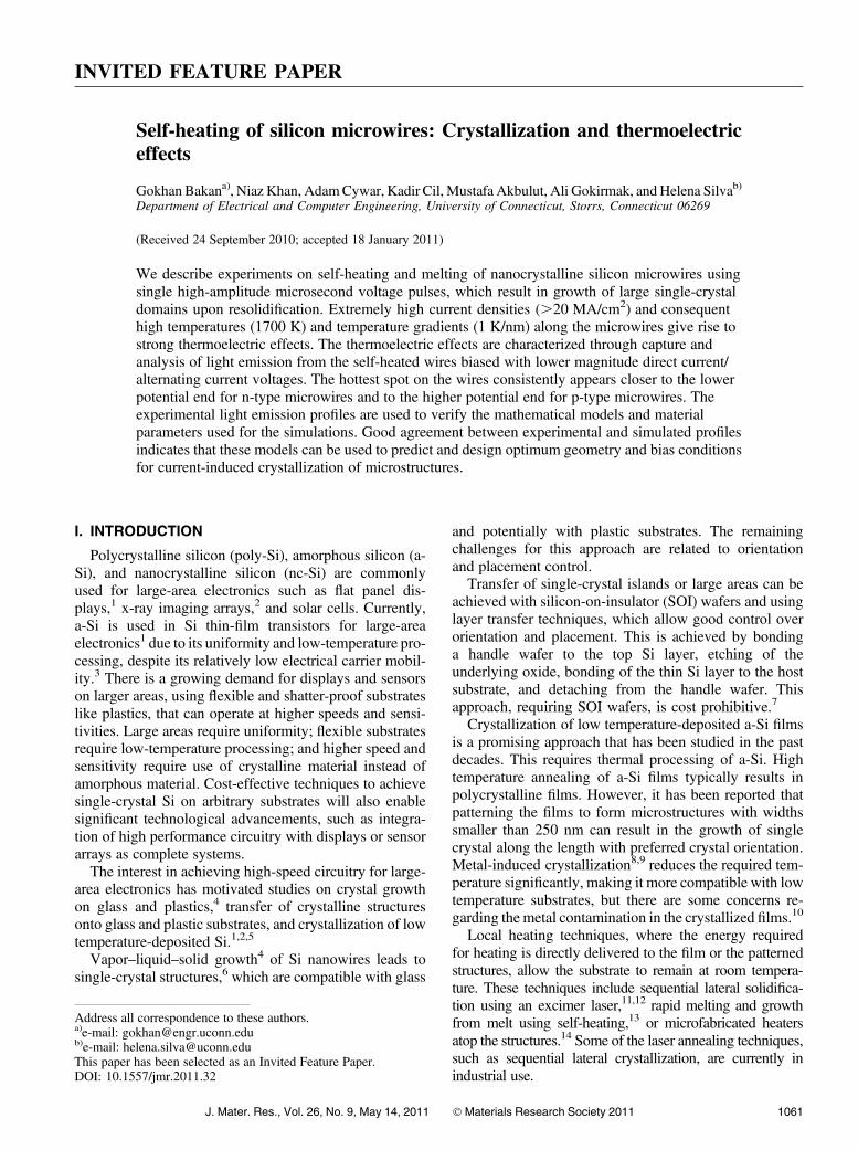
Simulation results for the pulsed wire are seen inFig. 14. The peak temperature on the wire reaches meltingtemperature of Si (1690 K) in 1 ls for 5.8 V, 1 ls voltagepulse [Fig. 14(a)]. The voltage pulse amplitude is chosento keep the peak temperature on the wire below the meltingtemperature because the phase change is not included inthe modeling. The time to reach the melting temperaturescales down as the voltage pulse amplitude is increased[Fig. 14(b)]. The simulations suggest that the peaktemperature on the wire can reach the melting temperaturein less than 10 ns for voltage pulse amplitudes larger than30 V. The cooling time of the wire is less than 250 ns forthe given geometry. The simulated temperature profilealong the wire just before melting is significantly skewedcompared to the profile simulated without thermoelectriceffects [Fig. 14(c)]. The peak temperature is closer tolower potential end of the wire, which is in agreement withprevious reports and our optical observations. Figure 14(c)suggests that the melting of the wire starts on one end andcontinues until the whole wire melts.
The light emission from the self-heated microwires isexpected to be due to blackbody radiation.24 The lightemission intensity profiles corresponding to the simulatedtemperature profiles are calculated using Eq. (5)24 in thevisible range to compare the simulated and experimentallight intensity results.
EðTÞ5Zk
eðk; TÞEðk;TÞ dk ; ð5Þ
where ε(k,T) is the emissivity of the microwires, which isassumed to be constant as it changes only very slightlythroughout the visible range for Si.38 E(k,T) is theblackbody radiation from the microwire as a function of
TABLE I. Room temperature values of the physical parameters usedfor the modeling.
ρ (X�cm) k (W/m�K) CP (J/kg�K) d (kg/m3) S (lV/K)
nc-Si 23 � 10�3a,b 54c 703d 2330d �105e,f
SiO2 1016d 1.38d 703d 2203d –
Si 10�1d 163d 703d 2330d –
aThis work, bRef. 18, cRef. 31, dRef. 29,eRef. 32, and fRef. 33.nc-Si, nanocrystalline silicon; SiO2, silicon dioxide; Si, silicon.
FIG. 13. Three-dimensional structure used for numerical modeling:a 2.5-lm long, suspended nc-Si microwire and pads on SiO2 over c-Sisubstrate. A single voltage pulse or a square signal with increasingamplitude is applied to the square section of the left pad, while thesquare section on the right pad and the bottom surface of the substrateare set to 0 V. The temperature at these electrical boundaries is kept at300 K.
G. Bakan et al.: Self-heating of silicon microwires: Crystallization and thermoelectric effects
J. Mater. Res., Vol. 26, No. 9, May 14, 20111068
radiation wavelength and temperature. The calculatedlight emission is convoluted using a point source approachto emulate the diffraction-limited experimental light in-tensity profiles.39 Each 1-nm segment of the microwire isassumed to be a point light source with a Gaussianintensity profile as given in Eq. (6).
IGaussianðxÞ5 IðxcenterÞffiffiffiffiffiffiffiffiffiffiffi2pr2
p e�ðx�xcenterÞ2
2r2 ; ð6Þ
where xcenter is the point where the Gaussian profile isevaluated, I(xcenter) is the blackbody radiation from thatpoint, and σ is the width for the profile. The opticalresolution of our system, calculated as 1.11k, where k isthe wavelength of the emitted light,39 was used for r. The
intensity profiles from each point source are addedtogether and scaled to have the same peak intensity asthe experimental profile.
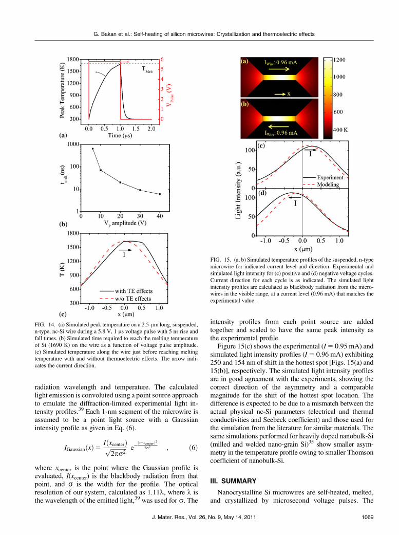
Figure 15(c) shows the experimental (I5 0.95 mA) andsimulated light intensity profiles (I5 0.96 mA) exhibiting250 and 154 nm of shift in the hottest spot [Figs. 15(a) and15(b)], respectively. The simulated light intensity profilesare in good agreement with the experiments, showing thecorrect direction of the asymmetry and a comparablemagnitude for the shift of the hottest spot location. Thedifference is expected to be due to a mismatch between theactual physical nc-Si parameters (electrical and thermalconductivities and Seebeck coefficient) and those used forthe simulation from the literature for similar materials. Thesame simulations performed for heavily doped nanobulk-Si(milled and welded nano-grain Si)35 show smaller asym-metry in the temperature profile owing to smaller Thomsoncoefficient of nanobulk-Si.
III. SUMMARY
Nanocrystalline Si microwires are self-heated, melted,and crystallized by microsecond voltage pulses. The
FIG. 14. (a) Simulated peak temperature on a 2.5-lm long, suspended,n-type, nc-Si wire during a 5.8 V, 1 ls voltage pulse with 5 ns rise andfall times. (b) Simulated time required to reach the melting temperatureof Si (1690 K) on the wire as a function of voltage pulse amplitude.(c) Simulated temperature along the wire just before reaching meltingtemperature with and without thermoelectric effects. The arrow indi-cates the current direction.
FIG. 15. (a, b) Simulated temperature profiles of the suspended, n-typemicrowire for indicated current level and direction. Experimental andsimulated light intensity for (c) positive and (d) negative voltage cycles.Current direction for each cycle is as indicated. The simulated lightintensity profiles are calculated as blackbody radiation from the micro-wires in the visible range, at a current level (0.96 mA) that matches theexperimental value.
G. Bakan et al.: Self-heating of silicon microwires: Crystallization and thermoelectric effects
J. Mater. Res., Vol. 26, No. 9, May 14, 2011 1069

crystallized microwires are under tensile stress andtypically acquire a cylindrical shape with smooth surfa-ces. Highly conductive continuous liquid Si paths formbetween the metal contacts and the wire followingpercolation paths on the Si pads. Significant reductionin resistivity and TEM analysis of a section of a pulsed,suspended microwire indicate crystallization of themicrowires upon resolidification, with growth of largesingle-crystal domains.
The extremely high current densities (.20 MA/cm2)and temperature gradients (~1 K/nm) reached along themicrowires result in strong thermoelectric effects asobserved through asymmetric heating of the microwires.These thermoelectric effects are analyzed through captureof asymmetric light emission from both n- and p-typemicrowires during slow voltage sweeps and low frequencyAC signals. The hottest spot is always closer to the lowerpotential end for n-type microwires and closer to thehigher potential end for p-type microwires. Low frequencyAC voltage applied to the microwires results in alternatinglocation of the hottest spot, confirming the thermoelectricnature of the observed asymmetric self-heating, rather thanbeing due to any asymmetric geometrical or thermalboundary condition. Characterization of Thomson effectthrough analysis of light emission from self-heated small-scale structures can be used as a tool to study non-equilibrium thermoelectric properties of materials andconfined geometries as compared to the equilibrium (nocurrent) Seebeck voltage.
Numerical modeling of the thermoelectric transport inan n-type microwire during an AC signal, includingtemperature-dependent physical parameters, shows goodagreement with the experiments. Simulation results fora microsecond voltage-pulsed microwire show signifi-cantly skewed temperature profiles for temperatures closeto melting temperature of Si, suggesting that this model canbe used to predict the heating and cooling of microwiresduring the rapid self-heating and crystallization process.
The findings of this work are relevant for studies oncrystallization techniques and thermoelectric effects un-der high current densities and thermal gradients. Higherperformance may be achieved for small-scale electronicdevices, such as PCMs, by accounting for thermoelectriceffects in device design.
ACKNOWLEDGMENTS
The devices were fabricated at the Cornell NanoScaleScience & Technology Facility. SEM imaging was par-tially performed at the Harvard Center for NanoScaleSystems. We thank Nathan Henry and Cicek Boztugfor their help with design and fabrication of the micro-wires. We also thank the CNF staff for their support forthe fabrication of the structures and Roger Ristau with theUniversity of Connecticut Institute of Materials Science
for TEM sample preparation and analysis. This work wassupported by the National Science Foundation (ECCS0702307, 0824171 and 0925973), the Department ofEnergy (DE-SC0005038) and the University of Connect-icut Research Foundation.
REFERENCES
1. S. Wagner, H. Gleskova, I.C. Cheng, and M. Wu: Silicon for thin-film transistors. Thin Solid Films 430, 15 (2003).
2. R.H. Reuss, B.R. Chalama, A.Moussessian, M.G. Kane, A. Kumar,D.C. Zhang, J.A. Rogers, M. Hatalis, D. Temple, G. Moddel, B.J.Eliasson, M.J. Estes, J. Kunze, E.S. Handy, E.S. Harmon, D.B.Salzman, J.M. Woodall, M.A. Alam, J.Y. Murthy, S.C. Jacobsen,M. Olivier, D. Markus, P.M. Campbell, and E. Snow: Macro-electronics: Perspectives on technology and applications. Proc.IEEE 93, 1239 (2005).
3. T. Makino and H. Nakamura: Electrical and optical properties ofboron doped amorphous silicon films prepared by CVD. Jpn. J.Appl. Phys. 17, 1897 (1978).
4. R.S. Wagner and W.C. Ellis: Vapor-liquid-solid mechanism ofsingle crystal growth. Appl. Phys. Lett. 4, 89 (1964).
5. T.I. Kamins: Polycrystalline Silicon for Integrated Circuits andDisplays (Kluwer Academics Publishers, Norwell, MA, 1998), p. 378.
6. Y. Cui, Z. Zhong, D. Wang, W.U. Wang, and C.M. Lieber: Highperformance silicon nanowire field effect transistors. Nano Lett. 3,149 (2003).
7. X. Shi, K. Henttinen, T. Suni, I. Suni, S.S. Lau, and M. Wong:Characterization of low-temperature processed single-crystallinesilicon thin-film transistor on glass. IEEE Electron Device Lett. 24,574 (2003).
8. Y.C. Wu, T.C. Chang, P.T. Liu, Y.C. Wu, C.W. Chou, C.H. Tu,J.C. Lou, and C.Y. Chang: Mobility enhancement of polycrystal-line-Si thin-film transistors using nanowire channels by pattern-dependent metal-induced lateral crystallization. Appl. Phys. Lett.87, 143504 (2005).
9. C.J. Su, H.C. Lin, and T.Y. Huang: High-performance TFTs with Sinanowire channels enhanced by metal-induced lateral crystalliza-tion. Electron Device Lett. IEEE 27, 582 (2006).
10. J.Y. Kim, J.W. Han, J.M. Han, Y.H. Kim, B.Y. Oh, B.Y. Kim, S.K.Lee, and D.S. Seo: Nickel oxide-induced crystallization of siliconfor use in thin film transistors with a SiN diffusion filter. Appl. Phys.Lett. 92, 143501 (2008).
11. R.S. Sposili and J.S. Im: Sequential lateral solidification of thinsilicon films on SiO. Appl. Phys. Lett. 69, 2864 (1996).
12. J.S. Im, R.S. Sposili, and M.A. Crowder: Single-crystal Si films forthin-film transistor devices. Appl. Phys. Lett. 70, 3434 (1997).
13. T. Sameshima, N. Andoh, and H. Takahashi: Rapid crystallizationof silicon films using electrical-current-induced joule heating.J. Appl. Phys. 89, 5362 (2001).
14. N. Andoh, T. Sameshima, and K. Kitahara: Crystallization ofsilicon films by rapid joule heating method. Thin Solid Films 487,118 (2005).
15. G. Bakan, A. Cywar, H. Silva, and A. Gokirmak: Melting andcrystallization of nanocrystalline silicon microwires through rapidself-heating. Appl. Phys. Lett. 94, 251910 (2009).
16. V.M. Glazov, S.N. Chizhevskaya, and N.N. Glagoleva: LiquidSemiconductors (Plenum Press, New York, 1969), p. 362.
17. H.S. Schnyders and J.B. Van Zytveld: Electrical resistivity andthermopower of liquid Ge and Si. J. Phys. Condens. Matter 8,10875 (1996).
18. H. Sasaki, A. Ikari, K. Terashima, and S. Kimura: Temperaturedependence of the electrical resistivity of molten silicon. Jpn. J.Appl. Phys. 34, 3426 (1995).
G. Bakan et al.: Self-heating of silicon microwires: Crystallization and thermoelectric effects
J. Mater. Res., Vol. 26, No. 9, May 14, 20111070

19. G. Bakan, K. Cil, A. Cywar, H. Silva, and A. Gokirmak: Measure-ments of liquid silicon resistivity on silicon microwires, in Semi-conductor Nanowires–Growth, Size-Dependent Properties andApplications, edited by P.C. McIntyre, J.M. Redwing, V. Schmidt,and S. Gradecak (Mater. Res. Soc. Symp. Proc. 1178E, Warrendale,PA, 2009), p. AA06-06.
20. S. Ayas, G. Bakan, N.E. Williams, A. Gokirmak, and H. Silva:Finite element simulation of filamentation in nanocrystalline siliconfilms under electrical stress. Presented at the 2010 MRS FallMeeting, Boston, MA, 2010; (AA17, 64).
21. N.E. Williams, E. Carpena, K. Cil, H. Silva, and A. Gokirmak:Temperature dependent electrical characterization and crystalliza-tion of nanocrystalline silicon. Presented at the 2010 MRS SpringMeeting, San Francisco, CA, 2010: (A17.9).
22. D.M. Rowe: Thermoelectrics Handbook: Macro to Nano (CRCPress, Florida, 2006).
23. D.K.C. MacDonald: Thermoelectricity: An Introduction to thePrinciples (Dover Publications, Mineola, NY, 2006), p. 133.
24. C.H. Mastrangelo, J.H.J. Yeh, and R.S. Muller: Electrical andoptical characteristics of vacuum-sealed polysiliconmicrolamps.IEEE Trans. Electron. Dev. 39, 1363 (1992).
25. O. Englander, D. Christensen, and L. Lin: Local synthesis of siliconnanowires and carbon nanotubes on microbridges. Appl. Phys. Lett.82, 4797 (2003).
26. A. Jungen, C. Stampfer, and C. Hierold, Thermography ona suspended microbridge using confocal Raman scattering. Appl.Phys. Lett. 88, 191901, 05/08 (2006).
27. D.K. Schroder: Semiconductor Material and Device Characteriza-tion (Wiley-Interscience, New York, 2006).
28. D. Tio Castro, L. Goux, G.A.M. Hurkx, K. Attenborough, R.Delhougne, J. Lisoni, F.J. Jedema, M.A.A. in9t Zandt, R.A.M.Wolters, D.J. Gravesteijn, M.A. Verheijen, M. Kaise, R.G.R.Weemaes, and D.J. Wouters: Evidence of the thermo-electric
Thomson effect and influence on the program conditions and celloptimization in phase-change memory cells, in IEEE InternationalElectron Devices Meeting, 2007, pp. 315–318.
29. COMSOL-Multiphysics Modeling Library, http://www.comsol.com.
30. E.M. Lifshitz, L.D. Landau, and L.P. Pitaevskii: Electrodynamicsof Continuous Media, 2nd ed. (Pergamon Press, MA, 1984),p. 455.
31. A.A. Geisberger, N. Sarkar, M. Ellis, and G.D. Skidmore: Electro-thermal properties and modeling of polysilicon microthermalactuators. J. Microelectromech. Syst. 12, 513 (2003).
32. M. Von Arx, O. Paul, and H. Baltes: Test structures to measure theSeebeck coefficient of CMOS IC polysilicon. IEEE Trans. Semi-cond. Manuf. 10, 201 (1997).
33. W. Fulkerson, J.P. Moore, R.K. Williams, R.S. Graves, and D.L.McElroy: Thermal conductivity, electrical resistivity, and seebeckcoefficient of silicon from 100 to 1300° K. Phys. Rev. 167, 765(1968).
34. T.H. Geballe and G.W. Hull: Seebeck effect in silicon. Phys. Rev.98, 940 (1955).
35. S.K. Bux, R.G. Blair, P.K. Gogna, H. Lee, G. Chen, M.S.Dresselhaus, R.B. Kaner, and J.P. Fleurial: Nanostructured bulksilicon as an effective thermoelectric material. Adv. Funct. Mater.19, 2445 (2009).
36. D.I. Jones, P.G. Le Comber, and W.E. Spear: Thermoelectric powerin phosphorus doped amorphous silicon.Philos. Mag. 36, 541 (1977).
37. C. Ong, E. Sin, and H. Tan: Heat-flow calculation of pulsed excimerultraviolet laser’s melting of amorphous and crystalline siliconsurfaces. J. Opt. Soc. Am. B 3, 812 (1986).
38. T. Sato: Spectral emissivity of silicon. Jpn. J. Appl. Phys. 6, 339(1967).
39. D.G. Brandon and W.D. Kaplan:Microstructural Characterizationof Materials, 2nd ed. (Wiley, New York, 1999), p. 536.
G. Bakan et al.: Self-heating of silicon microwires: Crystallization and thermoelectric effects
J. Mater. Res., Vol. 26, No. 9, May 14, 2011 1071