Corrugated Quantum-Well Infrared Photodetector Focal Plane Arrays
13
Corrugated Quantum Well Infrared Photodetector Focal Plane Array Test Results August 1999 A. Goldberg and K. K. Choi EO/IR Technology Branch, Army Research Laboratory, Adelphi, MD 20783 & N.C. Das, A. La, and M. Jhabvala, NASA Goddard Space Flight Center, Greenbelt, MD 20771 & R.B. Bailey, and K.Vural Rockwell Science Center, Thousand Oaks, CA 91360 ABSTRACT The corrugated quantum-well infrared photodetector (C-QWIP) uses total inter- nal reflection to couple normal incident light into the optically active quantum wells. The coupling efficiency has been shown to be relatively independent of the pixel size and wavelength thus making the C-QWIP a candidate for detectors over the entire infrared spectrum. The broadband coupling efficiency of the C-QWIP makes it an ideal candidate for multiwavelength detectors. We fabricated and tested C-QWIP focal plane arrays (FPAs) with cutoff wavelengths of 11.2 and 16.2 µm. Each FPA has 256 × 256 pixels that are bump-bonded to a direct injection readout circuit. Both FPAs provided Infrared imagery with good aesthetic attributes. For the 11.2-µm FPA, background-limited per- formance (BLIP) was observed at 60 K with f/3 optics. For the 16.2-µm FPA, BLIP was observed at 38 K. Besides the reduction of dark current in C-QWIP structures, the meas- ured internal quantum efficiency (η) remains to be high. The values for responsivity and quantum efficiency obtained from the FPA results agree well with those measured for single devices. 1. INTRODUCTION Over the past few years, quantum-well infrared photodetectors (QWIPs) have developed to the point that they can now be considered a serious alternative to the incumbent mercury-cadmium telluride (MCT) technology for infrared detection. This is especially true in multicolor applications and for wave- lengths beyond 12 μm (very long wavelength infrared or VLWIR), where MCT focal plane arrays (FPAs) become difficult to fabricate owing to the large relative changes in bandgap for small variations in mate- rial composition. In contrast, QWIP structures use the III-V material system for which the material growth and device processing technologies are more mature relative to those of II-VI materials like MCT. For detection of infrared wavelengths beyond 12 μm, the energy gap becomes less than 0.1 eV. The fabrication of uniform, large-format arrays of MCT photodiodes for such applications has proven to be difficult. QWIPs hold great promise in this arena for two reasons. First, the material composition Approved for public release; distribution is unlimited.
-
Upload
independent -
Category
Documents
-
view
3 -
download
0
Transcript of Corrugated Quantum-Well Infrared Photodetector Focal Plane Arrays

Corrugated Quantum Well Infrared Photodetector Focal Plane Array Test Results
August 1999
A. Goldberg and K. K. ChoiEO/IR Technology Branch, Army Research Laboratory, Adelphi, MD 20783
&N.C. Das, A. La, and M. Jhabvala,
NASA Goddard Space Flight Center, Greenbelt, MD 20771&
R.B. Bailey, and K.Vural
Rockwell Science Center, Thousand Oaks, CA 91360
ABSTRACTThe corrugated quantum-well infrared photodetector (C-QWIP) uses total inter-
nal reflection to couple normal incident light into the optically active quantum wells. Thecoupling efficiency has been shown to be relatively independent of the pixel size andwavelength thus making the C-QWIP a candidate for detectors over the entire infraredspectrum. The broadband coupling efficiency of the C-QWIP makes it an ideal candidatefor multiwavelength detectors. We fabricated and tested C-QWIP focal plane arrays(FPAs) with cutoff wavelengths of 11.2 and 16.2 µm. Each FPA has 256 × 256 pixelsthat are bump-bonded to a direct injection readout circuit. Both FPAs provided Infraredimagery with good aesthetic attributes. For the 11.2-µm FPA, background-limited per-formance (BLIP) was observed at 60 K with f/3 optics. For the 16.2-µm FPA, BLIP wasobserved at 38 K. Besides the reduction of dark current in C-QWIP structures, the meas-ured internal quantum efficiency (η) remains to be high. The values for responsivity andquantum efficiency obtained from the FPA results agree well with those measured forsingle devices.
1. INTRODUCTIONOver the past few years, quantum-well infrared photodetectors (QWIPs) have developed to the
point that they can now be considered a serious alternative to the incumbent mercury-cadmium telluride(MCT) technology for infrared detection. This is especially true in multicolor applications and for wave-lengths beyond 12 µm (very long wavelength infrared or VLWIR), where MCT focal plane arrays (FPAs)become difficult to fabricate owing to the large relative changes in bandgap for small variations in mate-rial composition. In contrast, QWIP structures use the III-V material system for which the materialgrowth and device processing technologies are more mature relative to those of II-VI materials like MCT.
For detection of infrared wavelengths beyond 12 µm, the energy gap becomes less than 0.1 eV.The fabrication of uniform, large-format arrays of MCT photodiodes for such applications has proven tobe difficult. QWIPs hold great promise in this arena for two reasons. First, the material composition
Approved for public release; distribution is unlimited.

Form SF298 Citation Data
Report Date("DD MON YYYY") 00081999
Report TypeN/A
Dates Covered (from... to)("DD MON YYYY")
Title and Subtitle Corrugated Quantum Well Infrared Photodetector Focal PlaneArray Test Results
Contract or Grant Number
Program Element Number
Authors Project Number
Task Number
Work Unit Number
Performing Organization Name(s) and Address(es) EO/IR Technology Branch Army Research Laboratory Adelphi,MD 20783
Performing Organization Number(s)
Sponsoring/Monitoring Agency Name(s) and Address(es) Monitoring Agency Acronym
Monitoring Agency Report Number(s)
Distribution/Availability Statement Approved for public release, distribution unlimited
Supplementary Notes
Abstract
Subject Terms
Document Classification unclassified
Classification of SF298 unclassified
Classification of Abstract unclassified
Limitation of Abstract unlimited
Number of Pages 12

(percentage of aluminum in the barrier layers) is not very challenging for the commonly used molecularbeam epitaxy (MBE) technique. Second, the quantum-well widths needed for such detectors are gener-ally greater than those used for QWIPs in the 8 to 12 µm region of the spectrum. This allows for lessvariation of the well widths (as a percentage of the mean) for long wavelength QWIPs relative to thosedesigned for shorter wavelengths.
There are, however, several issues that have kept QWIPs from being generally accepted as a de-tector structure for VLWIR applications. These issues are basically the same ones that confront QWIPsoperating in the more conventional 3 to 5 µm (mid-wave infrared or MWIR) and 8 to 12 µm (long waveinfrared or LWIR) bands. The two most important of these issues are: (1) high dark current and (2) lowresponsivity of QWIPs relative to MCT detectors operating in the same wavelength range and at the sametemperature.
The first issue, that of the relatively high dark current of QWIPs with respect to MCT, does nothave the overriding importance for VLWIR applications as it does for LWIR systems. Typically, VLWIRsystems are designed for space-based platforms (since very little VLWIR light penetrates the atmos-phere). That being the case, users are often willing to cool FPAs to temperatures as low as 40 K at whichpoint the noise due to the dark current of VLWIR QWIPs is expected to be lower than noise from othersources.
The problem of low quantum efficiency of QWIPs relative to MCT is very important. QWIPs donot respond well to normally incident light because of the electric dipole quantum mechanical selectionrule. Intersubband electron transitions (from the quantum-well ground state to an excited state) are al-lowed only if some component of the photon’s electric field is perpendicular to the barrier. To absorbnormally-incident light (for which the electric field is parallel to the barrier) some kind of optical cou-pling structure that rotates the propagation vector of the light must be incorporated in the pixel. Severaldifferent optical coupling structures have been proposed and demonstrated such as one-dimensional (lin-ear) diffraction gratings,1 two-dimensional gratings,2 and “random” gratings.3
In this paper we will present test results from QWIP FPAs made with a relatively new opticalcoupling scheme, the corrugated QWIP (or C-QWIP). Two FPAs were fabricated and hybridized to aread-out integrated circuit (ROIC) chip. The first of these arrays had a wavelength of maximum responseof 10.7 µm with a long wavelength cutoff of 11.2 µm; the second of these arrays had its peak wavelengthat 15.0 µm and a long wavelength cutoff of 16.2 µm.
2. Device FabricationTwo wafers, designated sample A and sample B, were grown and processed for this work. The
details of the growth and fabrication processes have been discussed elsewhere4 and will only be summa-rized here. The device structures, the so-called bound-to-quasibound QWIPs, were grown by MBE on
1 G. Hasnain, B. F. Levine, C. G. Bethea, R. A. Logan, J. Walker, and R. J. Malik, Appl. Phys. Lett., 54, 2515, 1989.2 J. Y. Anderson, L. Lundqvist, and Z. F. Paska, Appl. Phys. Lett., 59, 857, 1991.3 G. Sarusi, B. F. Levine, S. J. Pearton, S. V. Bandera, and R. E. Liebenguth, Appl. Phys. Lett., 64, 960, 1994.4 N.C. Das, K.K. Choi, A. C. Goldberg, A. La, M. Jhabvala, R.B. Bailey, and K.Vural, Fabrication and evaluation of11.2 and 16.2 µm cutoff C-QWIP arrays, Proceedings of the SPIE, Infrared Technology and Applications XXV, Vol.3387, Orlando, FL, 1999.

semi-insulating GaAs substrates. The well widths and barrier heights were designed such that sample Awould have maximum response at 10.7 µm and sample B would have maximum response at 15.0 µm. Inthe fabrication of a C-QWIP, wet chemical etching is used which leaves the surface with triangular corru-gations (hence the name corrugated QWIP) as shown in Figure 1 (a). Figure 1 (b) shows a top view ofmany pixels in an FPA. There is an unetched region in the center of each pixel where ohmic contactmetal and the indium bump are deposited. The size of the unetched island generally depends on the in-dium bump size.
Ohmic Contact
Substrate
QWIP
(a) (b)
Figure 1. The C-QWIP pixel in cross-section (a) showing a ray diagram of normally incident light as itsuffers total internal reflection inside the pixel and a top view of several pixels in a focal plane array (b).The pixel size is 40×40 µm2. There is an unetched island for the top contact metal and an unetched bridgeto group several corrugations into one pixel.
The detectors were processed into arrays of 256 × 256 pixels and then were hybridized to Rock-well TCM2550 ROICs. Due to problems with wafer processing, the hybridization of sample A was donewith no indium bumps on the detector side of the hybrid. As a result, large areas of the perimeter of thearray, about 20 percent of the total number of pixels, were inoperable. The hybridization of sample B wasmuch better, with only 1.6 percent of the pixels being inoperable.
A small piece of each wafer was used for single-pixel measurements. The results of these meas-urements are presented in detail elsewhere.5 The wavelength of maximum response was 10.7 µm forsample A and 14.9 µm for sample B with long wavelength cutoffs of 11.2 µm and 16.2 µm, respectively.These results match the spectral responses predicted from the design recipe. The spectral response oftypical devices from each wafer are shown in Figure 2.
The response spectra of the C-QWIP are compared with spectra from devices fabricated with nocorrugation. Light was coupled to the noncorrugated devices through 45° wedges polished in the sides oftheir substrates. It is evident that the C-QWIP design preserves the entire response spectrum of thequantum well (as opposed to diffraction gratings, which tend to be highly resonant).
5 K. K. Choi, C. J. Chen, L. P. Rohkinson, D. C. Tsui, N. C. Das, M. Jhobvala, M. Jiang, and T. Tamir, “CorrugatedQuantum Well Infrared Detector Arrays,” IRIS Proceedings of the Specialty Group on Detectors, Lexington, MA,1999.

(a)
8 9 10 11 12
Wavelength (µm)
0.0
0.1
0.2
0.3
0.4
0.5
Res
pons
ivity
(A/W
)
C-QWIP
45o coupling x 1.5
V = -2 V
(b)
10 11 12 13 14 15 16 17 18 19 20
Wavelength (µm)
0
1
2
3
4
Res
pons
ivity
(A/W
)
C-QWIP
45° COUPLING
V = +2 V
Figure 2. Spectral responsivity of samples A (a) and B (b). The wavelengths of maximum response are10.7 µm and 14.9 µm, respectively.
3. FPA Test Results3.1 Test Setup
Figure 3 is a block diagram of the system used to test the FPAs. The infrared source used was aCI-Systems Model SR-70 extended-area blackbody. Typically, the source temperature was varied from

20 °C to 40 °C. The system is capable of capturing many consecutive frames of images, either to theframegrabber’s memory (at the frame rate of the camera) or directly to the hard disk (at a reduced rate).
Clock card
Bias card
Dewar (MTD-150)A/D card, 12 bits @ 12 Mpixels/s
FPA
Camera head
Extended-areaBlackbody
Computerwith frame-grabber andsignalprocessor
RS-422
Figure 3. Block diagram of the FPA test setup. The clock card provides the six clock signals necessaryto run the FPA and the bias card provides the 6 required DC bias levels. The signals from A/D card aretransmitted to a computer over an RS-422 cable where they are converted to images by a framegrabber.The image data may then be stored to hard disk and/or displayed on a monitor.
The FPA drive electronics were built by SE-IR Corporation. The clock and bias generator cardsare located in the "camera head" just outside the dewar. These cards provide the six clock signals (pixelclock, line clock, frame clock, etc.) and the dc bias levels (VDD, detector bias, etc.) necessary to run theFPA. The FPA output is fed into a 12-bit analog-to-digital (A/D) converter that is rated at 1.2 × 10⁷ pix-els/s with less than 1 count of noise in the least significant bit (LSB). The input-referred noise level isapproximately 100 µV. The digitized signals from the A/D are transmitted to the computer over an RS-422 cable where they are converted to images by the framegrabber. The image data may then be stored toa hard disk and/or displayed on a monitor.
The tests on the arrays were done with the FPA installed in a liquid helium flow-through cryostat(Lakeshore MTD-150). The cryostat was equipped with an internal cooled aperture wheel that allowedfor operation of the FPA under a wide range of background flux conditions (including zero-backgroundfor dark current measurements). The widest cold aperture corresponded to a field of view of f/3.
3.2 Results and Discussion
The bias conditions for the FPAs are shown in table 1. The bias function DSUB is the substratebias. The actual bias across the detector is the difference between the value of DSUB and VDDA (theanalog power bias). The conditions shown in Table 1 correspond to a bias across the detectors of –2 V(as measured from the indium bump contact on the detectors to the substrate). A small amount of biasmay also be provided through the use of the DIGATE (direct injection gate) voltage. The other voltagelevels on the ROIC do not significantly affect the bias on the detectors.

Table 1. Bias conditions used for the C-QWIP FPAs.
Bias name Value (V)VDDA 5.058VDDD 4.998DIGATE 3.135COLPLUS 2.674DEADPOT 2.502DSUB 7.007
Generally, the FPA was run at a frame rate of 60 Hz. However, at low temperatures (~40 K)frame rates as low as 1 Hz were needed achieve integration times long enough to measure the dark current(under zero background conditions). For dark current measurements, the 0 field-of-view cold stop wasplaced in front of the FPA. The current was measured by integrating charge from the detectors for as longa time as necessary to fill the integration capacitor approximately half way to saturation. A number offrames (typically 50) were then collected and averaged. The current was then calculated using the ex-pression
I NG CAD=
τAmp (1)
where N is the number of counts, GAD is the gain of the A/D converter (volts/count), C is the capacitanceand τ is the integration time. The charge well capacity is 2 × 10⁷ electrons when FPA is run in snapshotmode. The output voltage swing was 2.2 V. The well capacitance, therefore, was 1.45 pF. Similar datawere collected with the shutter open (f/3 aperture) to measure the sum of the dark current and photocur-rent.
3.2.1 Dark Current and BLIP Temperature
We show the results of dark current and photocurrent measurements on samples A and B in Fig-ures 4 and 5, respectively. The dark current shows a clearly exponential dependence with temperature inboth samples. The deviation from this behavior at the lowest temperatures may be due to the photon fluxfrom the cold shield surfaces, which were at a temperature of approximately 80 K. If we define the tem-perature at which the current in the detectors generated by the background photon flux is equal to the darkcurrent as the background-limited infrared performance (BLIP) temperature, then the BLIP temperaturefor sample A is approximately 60 K and that for sample B is 39 K. We can calculate the conversion effi-ciency (quantum efficiency × photoconductive gain) from the amount of photocurrent when the device iswell below the BLIP temperature. For sample A, the background-induced current level is approximately400 pA. This implies a peak conversion efficiency of 9 percent. Taking into account that the photocon-ductive gain measured on single-pixel devices from the same wafer was 0.25 at –2 V bias, the quantumefficiency is 20 percent. This value of quantum efficiency takes into account the 70 percent transmissionof the dewar window but does not take into account the 30 percent loss of light from reflection off thesubstrate. The thermal activation energy calculated from the slope of the log of the dark current vs. 1/kTwas 91 meV for sample A and 67 meV for sample B. These correspond to wavelengths of 13.6 µm and18.5 µm, respectively. The background-induced photocurrent for sample B was 1.6 × 10⁻⁹ A and this im-plies a conversion efficiency of approximately 9 percent (similar to sample A). The gain measured onsingle pixels of sample B was approximately 1.0 at –2 V bias.4 The quantum efficiency is therefore ap-proximately 9 percent.

Figure 4. Mean dark current (squares) and total current (circles) for C-QWIP sample A as a function oftemperature (described as 1/kT). The logarithmic behavior of the dark current with 1/kT defines a thermalactivation energy of 96.6 meV.
Since the thermal activation energy depends strongly on the material growth parameters (wellwidth, barrier height, etc.) its uniformity is a good indication of the quality of the epitaxial growth. Fig-ure 6 shows a histogram (a) and an image (b) of the activation energy values for the pixels in sample Aand Figure 7 shows the same information for sample B. We see that the standard deviation of the activa-tion energy for the operable pixels of sample A (10.7 µm peak) was 1.5 meV, which was 1.55 percent ofthe mean. The standard deviation of the activation energy for sample B (15 µm peak) was 4.5 meV,which was 6.7 percent of the mean. This indicates that the QWIP structure parameters (well widths, Al-GaAs composition, etc.) were very uniform in sample A but not nearly so in sample B.

Figure 5. Mean dark current (squares) and total current (circles) for C-QWIP sample B as a function oftemperature (described as 1/kT). The logarithmic behavior of the dark current with 1/kT defines a thermalactivation energy of 67 meV.
(a)
92 94 96 98 100 1020.0
126.4
252.8
379.2
505.6
632.0
Thermal activation energy (meV)
Cou
nt
(b)
0 25 50 75 100 125 150 175 200 225
0
50
100
150
200
250
Column
Row
Figure 6. The histogram (a) and image (b) of the thermal activation energies for the pixels in sample A.The mean activation energy was 96.6±1.5 meV. The black areas in the image are the regions where theROIC and the detector array failed to contact each other during hybridization.

(a)
50 55 60 65 70 75 800
100
200
300
400
500
600
700
800
Thermal activation energy (meV)
Cou
nt
(b)
0 25 50 75 100 125 150 175 200 225
0
25
50
75
100
125
150
175
200
225
250
Column
Row
Figure 7. The histogram (a) and image (b) of the thermal activation energies for the pixels in sample B.The mean activation energy was 67±4.5 meV.
3.2.2 Noise-Equivalent Temperature Difference
Owing to an extraneous noise source inside the dewar, we were not able to accurately measurethe noise-equivalent temperature difference on these arrays. This noise has also prevented us from per-forming accurate 3D-noise analysis on the FPAs as of this writing. However, we can estimate the valueof the temporal NE∆T by making some reasonable assumptions. The noise of the A/D converter, Z0, isknown to be 0.6 -0.8 counts in the least significant bit when no signal is applied. The temporal noise atthe input of the A/D will be proportional to the square root of the number of electrons that are collected inthe charge well during each frame time. We assume that the number of electrons due to current from thedetector is much greater than the number due to noise generated in the ROIC. The number of noisecounts in each frame is then given by
Z Z Ie
eC G
Z NG Ce
eCG
Z NeCGtotal
AD
AD
AD AD
= + = + FHG
IKJFHG
IKJ = +0 0 0
1ττ
τCounts (2)
where we have substituted the expression for the current in equation (1). If the number of signal counts isapproximately 2000 (half of the total A/D range), the expected number of noise counts is approximately2. The NE∆T can then be calculated by multiplying the noise by the measured temperature sensitivity.That is, the temperature difference represented by each A/D count. The temperature sensitivity was cal-culated from uncorrected image data taken at different scene temperatures. The estimated temporalNE∆T is then given by
NE T Z T TN Ntotal
HIGH LOW
HIGH LOW
∆ ≈ −−
FHG
IKJ °C (3)

where THIGH and TLOW are the high and low scene temperatures, respectively and NHIGH and NLOW are thehigh and low response counts, respectively. Using equation (3), the NE∆Τ was calculated for samples Aand B. The results of these calculations are shown in Figure 8 for sample A at an operating temperatureof 50 K and Figure 9 for sample B at T = 30 K. At the respective temperatures, both FPAs were back-ground-limited. The mean NE∆T for the operable pixels of sample A was 30±2 mK and that for the en-tire array of sample B was 30±1.5 mK. The standard deviations of the NE∆T values imply that the uncor-rected response nonuniformity was 6.67 percent for sample A and 5.0 percent for sample B. In Figure 10,we show the variation of the NE∆T of both FPAs with operating temperature. Figure 11 shows the varia-tion of the nonuniformity of response (the standard deviation of the NE∆T distribution divided by themean value of NE∆T) for each array as functions of temperature. The uncorrected nonuniformity im-proves (decreases) as the temperature is lowered, even for temperatures well below the BLIP temperature.
(a)
24 26 28 30 32 340
125
250
375
500
625
750
NE∆T (m K)
Cou
nt
(b)0 25 50 75 100 125 150 175 200 225
0
50
100
150
200
250
Column
Row
Figure 8. Estimated NE∆T histogram (a) and image (b) for sample A at a temperature of 50K. The meanNE∆T was 30±2 mK.
(a)
25 27 29 31 33 350.0
102.6
205.3
307.9
410.5
513.1
615.8
718.4
821.0
NE∆T (mK)
Coun
t
(b) 0 25 50 75 100 125 150 175 200 225
0
25
50
75
100
125
150
175
200
225
250
Column
Row
Figure 9. Estimated NE∆T histogram (a) and image (b) for sample B at a temperature of 30K. The meanNE∆T was 30±1.5 mK.
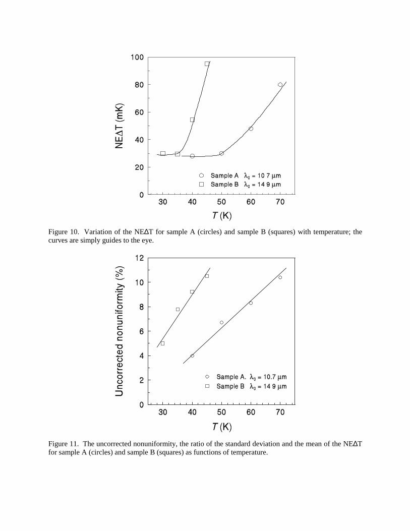
Figure 10. Variation of the NE∆T for sample A (circles) and sample B (squares) with temperature; thecurves are simply guides to the eye.
Figure 11. The uncorrected nonuniformity, the ratio of the standard deviation and the mean of the NE∆Tfor sample A (circles) and sample B (squares) as functions of temperature.

4. Summary and ConclusionsWe have measured the imaging characteristics of two C-QWIP focal plane arrays. The FPAs ex-
hibit relatively high values of quantum efficiency in agreement with previous single-pixel test results.The background-limited operating temperature (BLIP temperature) was found to be 60 K for the arraywith a peak wavelength of 10.7 µm and 39 K for the array with peak wavelength of 15 µm (for room-temperature background and an aperture of f/3) at a detector bias of –2 V. For an f/2 optical system, theBLIP temperatures for the arrays are expected to be slightly higher. Direct measurements of NE∆T couldnot be made due to extraneous system noise. However, under reasonable assumptions, NE∆T values forboth FPAs were calculated to be approximately 30 mK at temperatures below the BLIP temperature. Theuncorrected response nonuniformity at temperatures below the BLIP temperature was approximately 5percent for both arrays. This shows that the wet chemical etch needed to form the corrugations is uniformenough to produce FPAs with good uniformity. The pixel operability of sample A (peak wavelength 10.7µm) was only about 80 percent owing to the fact that it was hybridized with bumps only on the ROIC sideof the hybrid. The operability of sample B (15 µm peak wavelength) was much better being 98.4 percent.In the coming year, we hope to fabricate and test FPAs with peak wavelength less than 9 µm. Given thehigh quantum efficiency seen in C-QWIP detectors, these FPAs are expected to have BLIP temperaturesat or above 77 K. Finally, we show uncorrected laboratory images taken with the FPAs described in thispaper in Figure 12.
(a). (b).
Figure 12. Uncorrected IR imageries of a person taken with the 10.7 µm C-QWIP FPA at 64 K (a), and animage of a person’s hand taken by the 15 µm C-QWIP FPA at 38 K (b).