Highly efficient and low-cost multispectral photodetector based on ...
52
1 Highly efficient and low-cost broadband multispectral photodetector based on RF sputtered a-Si/Ti structure F. Djeffal 1, *, N. Boubiche 2 , H. Ferhati 1 , J. Faerber 3 , F. Le Normand 2 , N. Javahiraly 2 and T. Fix 2 1 LEA, Department of Electronics, University of Batna 2, Batna 05000, Algeria 2 MaCEPV/ ICube, Université de Strasbourg and CNRS, Strasbourg, France 3 IPCMS, Université de Strasbourg and CNRS, Strasbourg, France E-mails: [email protected] Tel/Fax: 0021333805494 Abstract In this paper, a new cost-effective multispectral photodetector (PD) based on amorphous- silicon (a-Si)/titanium (Ti) structure, which achieves a high UV-Visible-NIR photoresponse is elaborated. A new design strategy based on combining FDTD (Finite Difference Time Domain) with GA (Genetic Algorithm) was used to determinate the a-Si/Ti multilayer geometry providing the highest photoresponsivity in UV, Visible and NIR regions. The optimized structure is then fabricated using RF magnetron sputtering technique. A comprehensive analysis of the photodetector electrical, optical and structural properties was carried out. The sputtered a-Si/Ti multilayer was characterized by Scanning Electron Microscopy (SEM), X-ray diffraction (XRD), and UV-Visible-NIR absorption spectroscopy. The a-Si/Ti multilayer PD exhibits a high broadband absorbance of 80% over the UV and even NIR spectrum ranges [200nm-1100nm]. Moreover, photoelectrical characterization showed that the developed device exhibits an improved responsivity under UV, Visible and NIR lights (1.9 A/W at 365nm, 1.24 A/W at 550 nm and 0.93 A/W at 900 nm) and a high ION/IOFF ratio of 68 dB. The broadband multispectral photodetection property offered by the proposed a-Si/Ti multilayer PD opens a new route for the fabrication of promising alternative photodetectors for future high-performance and cost-effective optoelectronic systems. Key words: broadband; RF sputtering; multispectral; photodetector; a-Si/Ti. Manuscript Click here to access/download;Manuscript;aSi-Ti-photode.docx Click here to view linked References
-
Upload
khangminh22 -
Category
Documents
-
view
0 -
download
0
Transcript of Highly efficient and low-cost multispectral photodetector based on ...

1
Highly efficient and low-cost broadband multispectral photodetector
based on RF sputtered a-Si/Ti structure
F. Djeffal1,*, N. Boubiche2, H. Ferhati1, J. Faerber3, F. Le Normand2,
N. Javahiraly2 and T. Fix2
1 LEA, Department of Electronics, University of Batna 2, Batna 05000, Algeria 2MaCEPV/ ICube, Université de Strasbourg and CNRS, Strasbourg, France
3 IPCMS, Université de Strasbourg and CNRS, Strasbourg, France
E-mails: [email protected]
Tel/Fax: 0021333805494
Abstract
In this paper, a new cost-effective multispectral photodetector (PD) based on amorphous-
silicon (a-Si)/titanium (Ti) structure, which achieves a high UV-Visible-NIR photoresponse is
elaborated. A new design strategy based on combining FDTD (Finite Difference Time
Domain) with GA (Genetic Algorithm) was used to determinate the a-Si/Ti multilayer
geometry providing the highest photoresponsivity in UV, Visible and NIR regions. The
optimized structure is then fabricated using RF magnetron sputtering technique. A
comprehensive analysis of the photodetector electrical, optical and structural properties was
carried out. The sputtered a-Si/Ti multilayer was characterized by Scanning Electron
Microscopy (SEM), X-ray diffraction (XRD), and UV-Visible-NIR absorption spectroscopy.
The a-Si/Ti multilayer PD exhibits a high broadband absorbance of 80% over the UV and
even NIR spectrum ranges [200nm-1100nm]. Moreover, photoelectrical characterization
showed that the developed device exhibits an improved responsivity under UV, Visible and
NIR lights (1.9 A/W at 365nm, 1.24 A/W at 550 nm and 0.93 A/W at 900 nm) and a high
ION/IOFF ratio of 68 dB. The broadband multispectral photodetection property offered by the
proposed a-Si/Ti multilayer PD opens a new route for the fabrication of promising alternative
photodetectors for future high-performance and cost-effective optoelectronic systems.
Key words: broadband; RF sputtering; multispectral; photodetector; a-Si/Ti.
Manuscript Click here to access/download;Manuscript;aSi-Ti-photode.docx
Click here to view linked References

2
1. Introduction
Optoelectronic systems based on the Silicon-photonics platform are predicted to be the
most practical technology to meet the cost-effective, large bandwidth, and low power
consumption requirements [1-4]. Photodetectors (PDs), which are the key components of
optoelectronic communication systems, have received an important research interest due to
their large applications in biomedical imaging, optical wireless communication, light-
detection and robotics [4-8]. Several published works have developed new PD devices, which
can detect different wavelength bands ranging from UV to infrared by using adequate
semiconductor photosensitive materials with appropriate band-gap values [7-10]. Moreover,
the PDs can become more efficient in extensive applications when they are able to detect the
broadband multispectral radiations (UV-Visible-NIR) [10-12]. However, the development of
multispectral and broadband PDs mainly depends on the control and selection of the suitably
matched band-gap materials in order to cover the multispectral range, which is regarded quite
challenging. Several works have been proposed to overcome this challenge suggested
developing alternative materials and device structures for broadband multispectral
photosensing applications. In this context, new design methodologies and structures including
plasmonic nanoparticles, core-shell nanostructures, nanowires, metal oxides-based
heterojunction and quantum dots have been developed to achieve high broadband absorbance
characteristics [10-20]. Despite the capability of these designs to provide the broadband
multispectral photodetection, they require costly fabrication techniques and high thermal
budget. Additionally, the interface defects associated with different heterostructure materials
can affect the carrier transport efficiency and light trapping mechanism, thus limiting the
sensor photoresponsivity. In this context, researchers have turned out their focus towards the
use of 2D-materials and mono-layers in order to overcome these limitations. This is mainly
due to their broadband absorption capability, flexibility and high electron mobility [21-23].

3
Nevertheless, PDs based on 2D-materials reveal a low responsivity due to severe charge
recombination effects and its weak absorption behavior. Therefore, the development of novel
efficient and low-cost broadband multispectral photodetectors is required to improve the
capabilities of optoelectronic technology. Motivated by this concept, the present work aims at
developing a new low-cost and highly efficient multispectral photodetector based on RF
sputtered a-Si/Ti multilayer structure for Si-photonic applications. To the best of our
knowledge, no design techniques based on experiments assisted by numerical optimization
using FDTD and GA computations were conducted to develop broadband multispectral PDs
using a-Si/Ti multilayer structure. Accordingly, the optimized a-Si/Ti multilayer structure was
prepared using RF magnetron sputtering technique. Structural, optical and electrical
characterizations of the elaborated a-Si/Ti-based PD were carried out. It is revealed that the
developed PD demonstrates outstanding broadband multispectral absorption capabilities over
a wide spectrum range with high electrical performances. Therefore, the proposed approach
provides a sound pathway for developing broadband sensors based on simple and low-cost
structures for high performance Si-photonics applications.
2. Device design and experiments
The development of Broadband multispectral PDs based on a-Si material is extremely
difficult. This constraint is mainly due to the intrinsic limited absorption edge of this material.
To overcome this absorption limitation, in this work we investigate a new multispectral PD
based on non-hydrogenated a-Si dwells on introducing intermediate Ti ultra-thin layers. In
this context, Fig.1 (a) illustrates a cross-sectional view of the investigated a-Si/Ti multilayer-
based PD device, where highly transparent ITO thin layer is deposited at the top of the
structure to reduce the optical reflection losses [4]. The a-Si/Ti multilayer structure is
sputtered considered on a glass substrate. As it is shown in this Figure,
],...,,[],...,,[ 2121 TijTiTiTiSinSiSiSia ttttanddddd represent the thickness victor values

4
associated with the silicon and titanium layers, respectively. The thickness of the PD device is
ta-Si/Ti. For the numerical simulation framework, the optical properties (absorbance, reflectance
and transmittance) of the investigated PD structure are calculated using FDTD method
provided SILVACO software [24].
As far as we are concerned, the development of highly efficient and low-cost
multispectral sensors through intuiting the multi-layer structural, geometrical and electrical
parameters by using the well-known optical and electrical properties of PDs is not sufficient
to achieve the best electrical performances and highest photoresponsivity over a wide
spectrum range. Alternatively, we believe that sophisticated numerical optimization strategies
behaving like predictive simulations are required to forecast the sensor performance. In this
context, the use metaheuristic optimization approaches such as GA technique is a powerful
tool for identifying the optimal geometrical configuration of the a-Si/Ti multilayer structure to
achieve the highest multispectral photoresponsivity. To do so, Fig.1 (b) shows the flowchart
of the adopted hybrid design approach based on combined GA and numerical simulation
techniques. The optical device properties are simulated using 2D-FDTD method. More details
regarding the suggested modeling approach can be found in our previously published works
[25-27].
The simulated spectral absorbance using FDTD technique is explored to formulate the
objective (fitness) function, which will be minimized using GA-based optimization method.
The fitness function is given by the following formula
maxmin ,
1)(
AXFitness i (1)
where A represents the average absorbance over the spectral range of maxmin , with
nm200min and nm1100max are respectively the minimum and the maximum
wavelength values considered for broadband photosensing of PDs, Xi denotes the design

5
parameter vector. Various metals (Ag, Au, Ni and Ti) are introduced in the optimization
procedure. After carrying out the optimization procedure, the resulted design parameter victor
of the investigated a-Si/Ti multilayer active-film is given by
)3],7,8,9[,20],40,50,36,20[( jnmnmnmtnmtnmnmnmnmdX TiITOSiai . While the
optimized metal is the Titanium, the optimized PD structure reveals a very high average
absorbance of 83.6% over UV-Vis-NIR spectral range, indicating its broadband sensing
properties. This makes it a promising candidate for elaborating highly efficient and low-cost
multispectral photodetectors. This enhancement is attributed to the role of GA-based
optimization tool in selecting the appropriate multilayer structure through promoting
enhanced light-scattering effects. The obtained design will be used to elaborate the optimized
a-Si/Ti multilayer sensor, which is the main objective of the next part.
The elaboration of the optimized PD is based on three-step manufacturing processes. In
the beginning, glass substrates were ultrasonically cleaned up using an ultrasonic bath and
commercial detergent and then dried under a nitrogen jet procedure. Afterwards, successive
deposition of the optimized a-Si and Ti thin-films on the glass substrate was carried out using
RF magnetron sputtering technique (MOORFIELD MiniLab 060). To do so, p-type Si and Ti
targets with high purity of 99.99% were used. This experimental technique is commonly used
to elaborate high-quality thin-layers [28-30]. The sputtering process was performed in a pure
Ar atmosphere with a pressure of 1.5 Pa. The deposition parameters were carefully tuned in
order to obtain unhydrogenated a-Si state, Besides, the targets to substrate distances were kept
at 6.5 cm and 5.1 cm for the Titanium and Si materials, respectively. The sputtering
deposition parameters for all sub-layers are summarized in Table.1. The ITO ultrathin film
was deposited on the sputtered a-Si/Ti multilayer by using targets with 90 wt% In2O3 and 10
wt% SnO2. It is worthy to note that the RF sputter was calibrated before the deposition of

6
deferent thin films, where each layer was separately grown on glass substrates to select the
appropriate deposition parameters.
In order to assess the optoelectronic performances of the fabricated sensor, structural and
optical characterizations were conducted using X-ray diffraction measurements (ARL
Equinox 3000) for 2 diffraction angle scans of [25°-80°] and UV-Visible-NIR
spectrophotometer (F10-RT-UV). The morphological characteristics of the prepared sample
were analyzed using scanning electron microscopy (SEM), where the surface (top) was
imaged with a Zeiss Gemini SEM 500 with a field emission Schottky source. The
semiconductor characterization system (Keithley 4200-SCS) was employed to measure the
current-voltage characteristics of the prepared device under dark and illumination conditions.
3. Results and discussions
The aim of this work is to investigate the role of introducing a-Si/Ti multilayered
structure with optimized geometry in improving the photosensing performances of PDs over a
wide spectral range. The structural properties of the prepared sample based on embedded a-Si
and Ti sputter-deposited thin-films are investigated using XRD technique. In this context,
Fig.2 (a) shows XRD measurements for (2) diffraction angle scanning from 25° to 80° of the
prepared samples based on ITO/a-Si thin-film and a-Si/Ti multilayered structure. The XRD
pattern of the elaborated sample with ITO/a-Si shows a low-intensity XRD peak indexed to
the (222) crystal plane of the ITO material. It can be also seen from this spectra the presence
of a diffraction peak at 28.5° angle, corresponding the (111) facets of silicon. This indicates
that the sputtering of thick Si films (ta-Si=130 nm) enables the formation of Si microcrystals.
However, it can be noticed from the XRD pattern of the elaborated a-Si/Ti multilayer
structure depicted in Fig.2 (a), the amorphous state of the silicon and ITO sputtered layers,
where no coherent XRD peaks are matching these materials. The obtained crystalline
characteristics can be explained by the ultralow thickness of the deposited silicon sub-layers,

7
which can prevent reaching the crystallization phase of the Si material. On the other hand, this
pattern demonstrates the presence of crystallized Ti metal, manifesting (101)-oriented film at
the diffraction angle of 39.5°. This highlights the beginning of the crystallization phase of the
deposited Ti inter-layers. Fig.2 (b) shows the SEM top surface image of the fabricated ITO/a-
Si/Ti multilayered sample. It can be seen from this micrograph that granulated ITO surface
with roughness characteristics is observed. This indicates that the growth is essentially
columnar for the embedded a-Si and Ti sub-layers, which further explains the obtained
amorphous state of the sputtered silicon thin-films as it is shown in Fig.2 (a). In other words,
as the a-Si and Ti thin-films are embedded by RF sputtering technique, the structure
roughness significantly increases and when the grain size is superior to the film thickness, the
growth becomes columnar particularly for the deposited layers closest to the surface.
One of the most important criteria that active layers of multispectral PDs should satisfy is
to offer a broadband absorption property. To assess the absorption capabilities of the prepared
sample based on stacked a-Si and Ti sub-layers with optimized geometry, the absorbance
spectra of the elaborated samples were extracted and illustrated in Fig.3. It can be observed
from this figure that significant changes concerning the optical behavior of the PD active film
are achieved by inserting an optimized a-Si/Ti multilayer. It demonstrates highly improved
absorption efficiency exceeding 80% over UV-Vis-NIR spectral range as compared to that of
a-Si thin-film (28.2%). This yields a high relative enhancement of 183%. In addition, the
obtained experimental results are found in a good agreement with the theoretical ones, thus
indicating the accuracy of the exploited numerical modeling technique. This achievement is
due to the effectiveness of the introduced FDTD-GA hybrid approach in promoting enhanced
light trapping capabilities of embedded a-Si and Ti sub-layers with suitable geometry. In other
words, the introduction of Ti intermediate metal films within the a-Si layer can generate
optical micro-cavities, which leads to extend the optical path in the PD active layer thereby

8
resulting in a broadband absorption characteristic. Therefore, the fabrication of such an
optimized a-Si/Ti multilayered structure as an MSM photodetector can extend the light
harvesting capability into the visible and NIR spectral ranges, making it very promising
candidate for the development of high-responsivity broadband PDs at low-cost.
To further investigate the multispectral photoresponse of the prepared PD based on
stacked a-Si and Ti thin-films, the sample is realized as an MSM photodetector. In this
framework, top and bottom gold contacts were evaporated via E-beam evaporation technique
as it is shown in Fig.1 (a). The fabricated device was then illuminated by monochromatic light
signals with wavelength values of 365 nm, 550 nm and 900 nm using LED lamps.
Consequently, the measured I-V characteristics in darkness and under illumination conditions
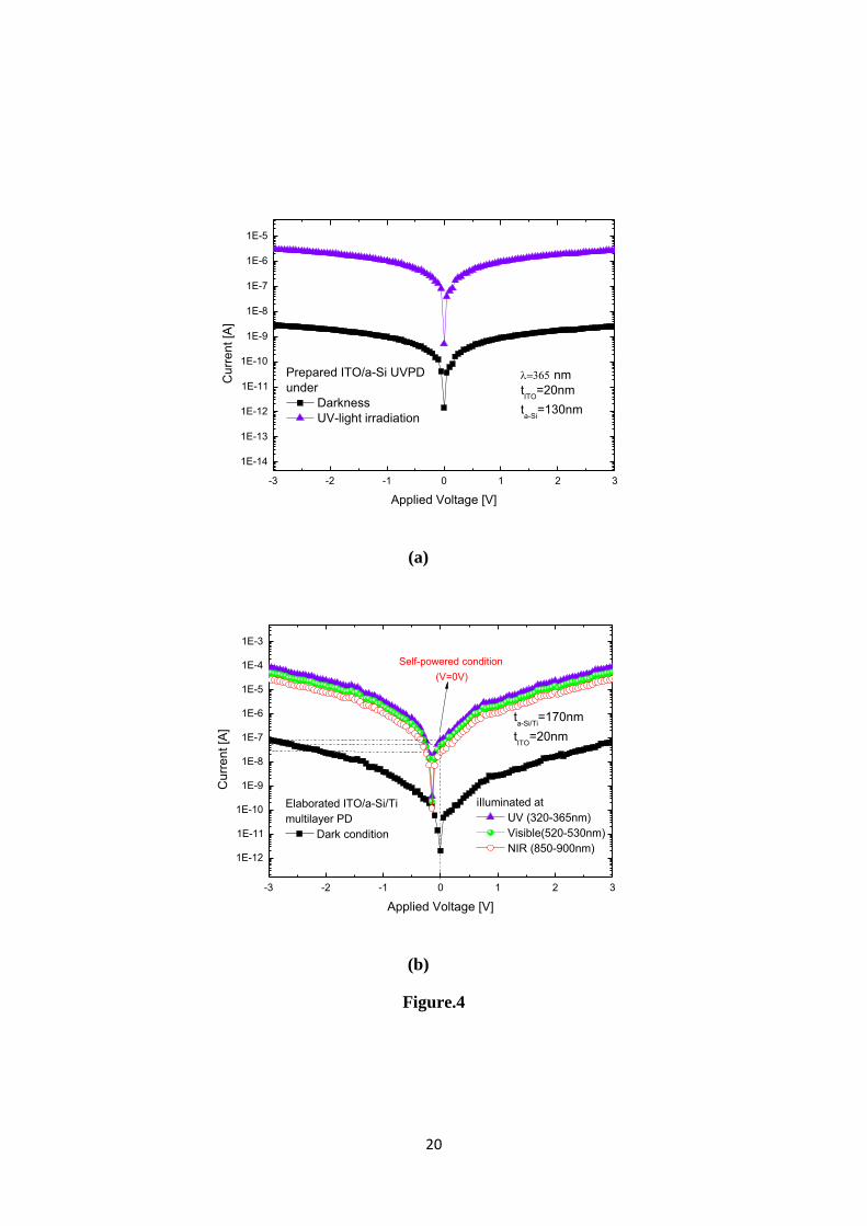
of the prepared sensors based on a-Si and a-Si/Ti multilayer active films are depicted in Fig.4
(a) and (b) respectively. It can be seen from Fig.4 (a) that the a-Si based PD shows a good
photoresponse only in the UV range. On the other hand, Fig.4 (b) demonstrates the ability of
the prepared PD with embedded a-Si and Ti sub-layers for providing multispectral
photodetection capability. The device shows excellent sensing properties with high
photocurrent values of 0.68 mA, 0.22 mA and 0.1 mA under UV, visible and NIR lights,
respectively at an applied voltage of 3V. Such finding correlates well with the above-outlined
broadband absorption characteristic of the optimized structure based on embedded a-Si and Ti
thin-films. Basically, the latter structure shows an extended absorption to the visible and NIR
regions, which can enables enhancing the carrier generation mechanism. This effect leads to
achieve an improved broadband photoresponse. Moreover, the use of stacked a-Si and Ti
layers can enlarge the depletion layer in the active layer due to the Schottky nature of the a-
Si/Ti contact. This can in turn improve the separation mechanism of the photo-excited e/h
pairs, thus reducing recombination losses. It can be also observed from this figure that the
proposed PD based on a-Si/Ti multilayer provides a favorable photocurrent at self-powered

9
condition, where the measured I-V curves are shifted to negative voltages. This phenomenon
is attributed to the degraded homogeneity of the deposited sub-layers, where the sputtering of
a-Si and Ti layers closest to the surface is principally columnar as it is above-outlined.
To show the capability of the proposed experiment assisted by FDTD-GA hybrid
approach in developing broadband PDs based on simple and low-cost structures, Fig.5 depicts
the measured spectral responsivity of the elaborated samples based on a-Si thin-film and
stacked a-Si and Ti layers. Clearly, the proposed sensor demonstrates a high responsivity over
a large spectral band from UV to NIR as compared to the conventional device. The prepared
PD with a-Si/Ti multilayered active film exhibits superior responsivity values of 1.9 A/W,
1.24A/W and 93 mA/W under UV, visible and NIR illumination conditions, respectively.
This multispectral photoresponse can be attributed to the role of introducing inter-metallic
layer in promoting enhanced antireflection capabilities. Besides, the use of an effective
approach based on experiment assisted by combined FDTD-PSO design methodology enables
enhancing the photogeneration/collection efficiency.
To show the strength of the prepared multispectral PD based on a simple and low-cost
embedded a-Si and Ti thin-films as compared to recently developed ones, a comparative
performance analysis is carried out. Accordingly, the associated FoM parameters including
current ratio (ION/IOFF ratio), responsivity and detectivity are extracted and summarized in
Table.2. This table confirms the ability of the optimized structure for outperforming other
perovskite, silicon and nanostructured multispectral PD structures in terms of FoM parameters
[31-40]. Although some reported devices demonstrated superior visible photoresponse, they
either exhibited a compromised UV sensitivity, stability issues and/or required the use of
critical raw materials and processing complexity. Alternatively, the present PD with stacked a-
Si and Ti thin-films provides a new strategy for achieving high and broadband photosensing
characteristics at low manufacturing cost. These results clearly demonstrate the great potential

10
of the proposed a-Si/Ti multilayer structure for multispectral photodetection application.
4. Conclusion
In this work, we have developed a new high-photoresponsivity multispectral PD based on
ITO/a-Si multilayer structure. The numerical simulation and optimization of the structure using
combined FDTD-GA approach offer improved photoresponsivity and broadband absorption
capabilities. The optimized design was employed in fabricating multispectral photodetector
using RF magnetron sputtering technique. The device structural and optical properties were
investigated using XRD and UV-Vis-NIR spectroscopy methods. It was found that excellent
UV-Vis-NIR absorbance with over than 80% average value was recorded which can lead to
improve the device photoresponsivity. In this context, the elaborated sensor offers ultra-high
responsivity values of 1.9 A/W, 1.24A/W and 0.93 A/W under UV, visible and NIR
illumination, respectively. This multispectral photodetection property is mainly attributed to
the effective light-management provided by the optimized design. Moreover, it is
demonstrated that the elaborated PD based on embedded a-Si and Ti sub-layers can operate in
self-powered mode, showing a favorable photocurrent of 0.4 µA. The proposed elaboration
methodology can contribute in a fascinating breakthrough towards broadband multispectral
photodetector devices based on Si-photonics platform.

11
References
[1] D. A. B. Miller, “Optical interconnects to silicon,” IEEE J. Sel. Top. Quantum Electron.,
vol. 6, pp. 1312-1317, 2000.
[2] C. Sun, et al “Single-chip microprocessor that communicates directly using light,” Nature,
vol. 528, pp. 534-538, 2015.
[3] S. Manipatruni, M. Lipson, and I. A. Young, “Device Scaling Considerations for
Nanophotonic CMOS Global Interconnects,” IEEE J. Sel. Top. Quantum Electron., vol.
19, pp. 1077-1086 , 2013.
[4] H. Ferhati, F. Djeffal, A. Saidi, A. Benhaya, A. Bendjerad, “Effects of annealing process
on the structural and photodetection properties of new thin-film solar-blind UV sensor
based on Si-photonics technology,” Mater. Sci. Semicond. Process., Vol.121, pp. 105331,
2021.
[5] W. Ouyang, F. Teng, J.-H. He, X. Fang, “Enhancing the Photoelectric Performance of
Photodetectors Based on Metal Oxide Semiconductors by Charge-Carrier Engineering,”
Adv. Funct. Mater., vol. 29, pp.1807672, 2019.
[6] H. Ferhati, F. Djeffal, “A Novel High-Performance Self-Powered Ultraviolet
Photodetector: Concept, Analytical Modeling and Analysis,” Superlattices Microstruct.,
vol. 112, pp.480-492, 2017.
[7] M. Zhang, D. Zhang, and F. Jing, “Hybrid Photodetector Based on ZnO Nanofiber
Polymers with High Spectrum Selectivity,” IEEE Photon. Technol. Lett., vol. 28, pp.
1677-1679, 2016.
[8] N. Naderi, M. Moghaddam, “Ultra-sensitive UV sensors based on porous silicon carbide
thin films on silicon substrate,” Ceramics International., Vol. 46, pp. 13821-138260, 2020.
[9] C. Li, W. Huang, L. Gao, H. Wang, L. Hu, T. Chen and H. Zhang, “Recent advances in
solution-processed photodetectors based on inorganic and hybrid photo-active materials,”
Nanoscale, vol.12, pp. 2201-2227, 2020.
[10] K. Benyahia, F. Djeffal, H. Ferhati, A. Bendjerad, A. Benhaya, A. Saidi,“ Self-
powered photodetector with improved and broadband multispectral photoresponsivity
based on ZnO-ZnS composite,” J. Alloy. Compd., vol. 859, pp.158242, 2021.
[11] H. S. Nalwa, “A review of molybdenum disulfide (MoS2) based photodetectors: from
ultra-broadband, self-powered to flexible devices,” RSC Adv., vol.10, pp. 30529, 2020.

12
[12] C. Ji, X. Huang, D. Wu, Y. Tian, J. Guo, Z. Zhao, Z. Shi, Y. Tian, J. Jie, and X. Li,
“Ultrasensitive self-driven broadband photodetector based on 2D-WS2/GaAs type-II
Zener heterojunction,” Nanoscale, vol.12, pp. 4435-4444, 2020.
[13] J. Miao and F. Zhang, “Recent progress on highly sensitive perovskite
photodetectors,” J. Mater. Chem. C, vol.7, pp. 1741-1791, 2019.
[14] J. Huang, J. Jiang, L. Hu, Y. Zeng, S. Ruan, Z. Ye and Y-J. Zeng, “Self-powered
ultraviolet photodetector based on CuGaO/ZnSO heterojunction,” J. Mater. Sci.: Mater.
Electron., vol.55, pp. 9003-9013, 2020.
[15] X. Xu, J. Chen, S. Cai, Z. Long, Y. Zhang, L. Su, S. He, C. Tang, P. Liu, H. Peng and
X. Fang, “A Real-Time Wearable UV-Radiation Monitor based on a High-Performance p-
CuZnS/n-TiO2 Photodetector”, Adv. Mater., vol. 25, pp. 1803165, 2018.
[16] M. Patel, P. M. Pataniya, V. Patel, C. K. Sumesh and D. J. Late, “Large area,
broadband and highly sensitive photodetector based on ZnO-WS2/Si heterojunction,”
Solar energy, vol.206, pp. 974-982, 2020.
[17] H. Ferhati and F. Djeffal, “High-Responsivity MSM Solar-Blind UV Photodetector
Based on Annealed ITO/Ag/ITO Structure Using RF Sputtering,” IEEE Sens. J., vol. 19,
pp. 7942 - 7949, 2019.
[18] S. Bhandari, D. Mondal, S. K. Nataraj and R. G. Balakrishna, “Biomolecule-derived
quantum dots for sustainable optoelectronics,” Nanoscale Adv., vol.1, 913-936, 2018.
[19] S. Li, Y. Zhang, W. Yang, H. Liuand and X. Fang, “2D Perovskite Sr2Nb3O10 for
High-Performance UV Photodetectors,” Adv. Mater., vol.32, pp. 1905443, 2020.
[20] T. T. Nguyen, M. Patel and J. Kim, “Self-powered transparent photodetectors for
broadband applications,” J. Surf. Interfac., vol.23, pp. 100934, 2021.
[21] B. Wang, Shi P. Zhong, Z. B. Zhang, Z. Q. Zheng, Y. P. Zhang and H. Zhang,
“Broadband photodetectors based on 2D group IVA metal chalcogenides
semiconductors,” Appl. Mater. Today, vol.15, pp. 115-138, 2019.
[22] C-H. Liu, Y-C. Chang, T. B. Norris and Z. Zhong, “Graphene photodetectors with
ultra-broadband and high responsivity at room temperature,” Nat. Nanotechnol., vol. 9, pp.
273–278, 2014.
[23] J. Yao and G. Yang, “2D material broadband photodetectors,” Nanoscale, vol. 12, pp.
454-476, 2020.
[24] Atlas User’s manual, SILVACO TCAD, 2012.

13
[25] F. Srairi, F. Djeffal and H. Ferhati,“ Efficiency increase of hybrid organic/inorganic
solar cells with optimized interface grating morphology for improved light trapping,”
Optik, vol. 130, pp. 1092-1098, 2017.
[26] H. Ferhati, F. Djeffal, “Role of Optimized Grooves Surface -Textured Front Glass in
improving TiO2 Thin Film UV Photodetector Performance,” IEEE Sens. J., vol. 16, pp.
5618- 5624, 2016.
[27] F. Djeffal, H. Ferhati, “A new high-performance phototransistor design based on both
surface texturization and graded gate doping engineering,” J. Comput. Electron, vol. 15,
pp. 301–310, 2016.
[28] E. Márquez, E. Saugar, J. M. Díaz, C. García-Vázquez, S. M. Fernández-Ruano, E.
Blanco, J. J. Ruiz-Pérez and D. A. Minkov, “The influence of Ar pressure on the structure
and optical properties of nonhydrogenated a-Si thin films grown by rf magnetron
sputtering onto room temperature glass substrates”, J. Non-Cryst Solids, vol. 517, pp. 32-
43, 2019.
[29] S. Y. Lee, Y. S. Park, T. Seong, “Optimized ITO/Ag/ITO multilayers as a current
spreading layer to enhance the light output of ultraviolet light-emitting diodes,” J. Alloy.
Compd., vol.776, pp. 960-964, 2019.
[30] A. Benhaya, F. Djeffal, K. Kacha, H. Ferhati, A. Bendjerad, “Role of ITO ultra-thin
layer in improving electrical performance and thermal reliability of Au/ITO/Si/Au
structure: An experimental investigation,” Superlattices Microstruct., vol.120, pp. 419-426,
2018.
[31] H. Ahmad, N. Afzal, M. Rafique, A. A. Ahmed, R. Ahmad and Z. Khaliq, “Post-
deposition annealed MoO3 film based high performance MSM UV photodetector
fabricated on Si(100),” Ceramics International, vol. 47, pp. 20477-20487, 2020.
[32] D. Wu, J. Guo, J. Du, C. Xia, L. Zeng, Y. Tian, Z. Shi, Y. Tian, K. J. Li, Y. H. Tsang
and J. Jie, “Highly Polarization-Sensitive, Broadband, Self-Powered Photodetector Based
on Graphene/PdSe2/Germanium Heterojunction,” ACS Nano, vol. 13, pp. 9907−9917,
2019.
[33] Y. Zhang, W. Xu, X. Xu, J. Cai, W. Yang, and X. Fang, “Self-Powered Dual-Color
UV–Green Photodetectors Based on SnO2 Millimeter Wire and Microwires/CsPbBr3
Particle Heterojunctions”, J. Phys. Chem. Lett., vol. 10, pp. 836–841, 2019.
[34] C. L. Hsu, H. Y. Wu, C. C. Fang, and S. P. Chang, “Solution-Processed UV and
Visible Photodetectors Based on Y-Doped ZnO Nanowires with TiO2 Nanosheets and Au
Nanoparticles,” ACS Appl. Mater. Interfaces, vol.5, pp. 2087-2095, 2018.

14
[35] M. Das, S. Sarmah, D. Barman, B. K. Sarma and D. Sarkar, “Distinct band UV–
Visible photo sensing property of ZnO-Porous silicon (PS): p-Si hybrid MSM
heterostructure,” Mater. Sci. Semicond. Process., vol.118, pp. 105188, 2020.
[36] F. Cao, W. Tian, K. Deng, M. Wang and L. Li, “Self‐Powered UV–Vis–NIR
Photodetector Based on Conjugated‐Polymer/CsPbBr3 Nanowire Array,” Adv. Funct.
Mater., vol.29, pp. 1906756, 2019.
[37] H. Ferhati, F. Djeffal and N. Martin, “Highly improved responsivity of self-powered
UV–Visible photodetector based on TiO2/Ag/TiO2 multilayer deposited by GLAD
technique: Effects of oriented columns and nano-sculptured surface,” Appl. Surf. Sci.,
vol.529, pp. 147069, 2020.
[38] M. S. Mahdi, K. Ibrahim, N. M. Ahmed, A. Hmood, F. I. Mustafa, S. A. Azzez and M.
Bououdina, “High performance and low-cost UV–Visible–NIR photodetector based on tin
sulphide nanostructures,” J. Alloy. Compd., 735, 2256-2262, 2018.
[39] Z. Zheng, L. Gan, J. Zhang, F. Zhuge and T. Zhai, “An enhanced UV–Vis–NIR and
flexible photodetector based on electrospun ZnO nanowire array/PbS quantum dots film
heterostructure,” Adv. Sci., vol.4, pp.1600316, 2017.
[40] G. Chatzigiannakis, A. Jaros, R. Leturcq, J. Jungclaus, T. Voss, S. Gardelis and M.
Kandyla, “Laser-Microstructured ZnO/p-Si Photodetector with Enhanced and Broadband
Responsivity across the Ultraviolet–Visible–Near-Infrared Range,” ACS Appl. Electron.
Mater., vol.9, pp. 2819–2828, 2020.

15
Figures caption:
Fig.1 (a): Device structure with MSM Schottky PD configuration based on the proposed a-Si/
Ti multilayer structure. (b) Flowchart of the adopted hybrid design approach based on
combined GA and numerical simulation techniques.
Fig.2 (a) X-ray diffraction patterns of the elaborated a-Si/Ti structure with ta-Si/Ti=170nm and
tITO=20nm. (b) SEM images of top surface of the elaborated a-Si/Ti multilayer structure using
RF magnetron sputtering technique.
Fig.3: Absorbance spectra of the prepared ITO/a-Si and a-Si/Ti multilayer samples with ta-Si/Ti
=170nm and tITO=20nm.
Fig.4: Measured I-V characteristics under dark and light-exposure conditions in UV, visible
and NIR spectrum bands of (a) the conventional device with a-Si active layer, (b) the
prepared PD based on embedded a-Si and Ti sub-layers.
Fig.5: Spectral photoresponsivity of the prepared PD structures based on a-Si thin-film and a-
Si/Ti multilayer.

16
Tables:
Table.1: Deposition parameters of the sputtered ITO/a-Si/Ti multilayer structure.
Table.2: Overall performance comparison between the elaborated PD and several reported
multispectral photodetector devices.

17
(a)
(b)
Figure.1
(b)
Figure.1
PD design parameters
)],,...,,[,],,,[( 21321jtttttdddtX TijTiTiTiITOSiaSiSiaSiai
FDTD optical modeling
Stop criteria Min
Fitness(Xi)
Optimized a-Si/Ti
multispectral PD
multilayer structure
No
Yes
GA technique to maximize the
average absorbance over a wide
spectrum range of [ max - max ]
ITO
a-Si
Glass substrate
a-Si
Ti metallic sub-
layer
da-Si 1
tTi1
tITO
Ti
Au
Gold contact

18
30 45 60 75
Ti(101)
Si(111)
ITO(222)
Inte
nsity (
a.u
)
deg
Conventional ITO/a-Si/Glass
structure
Prepared ITO/a-Si/Ti multilayered structure
(a)
(b)
Figure.2
50 nm
100nm
a-Si
20nm

19
200 400 600 800 100010
20
30
40
50
60
70
80
90
100
Ab
so
rba
nce
[%
]
Wavelength [nm]
Conventional ITO/a-Si thin-film
Elaborated ITO/a-Si/Ti superlattice
structure
Figure.3
20
-3 -2 -1 0 1 2 3
1E-14
1E-13
1E-12
1E-11
1E-10
1E-9
1E-8
1E-7
1E-6
1E-5
nm
tITO
=20nm
ta-Si
=130nm
Cu
rre
nt [A
]
Applied Voltage [V]
Prepared ITO/a-Si UVPD
under
Darkness
UV-light irradiation
(a)
-3 -2 -1 0 1 2 3
1E-12
1E-11
1E-10
1E-9
1E-8
1E-7
1E-6
1E-5
1E-4
1E-3
Self-powered condition
(V=0V)
ta-Si/Ti
=170nm
tITO
=20nm
iIluminated at
UV (320-365nm)
Visible(520-530nm)
NIR (850-900nm)
Elaborated ITO/a-Si/Ti
multilayer PD
Dark condition
Cu
rre
nt [A
]
Applied Voltage [V]
(b)
Figure.4

21
0.0
0.5
1.0
1.5
2.0
2.5
3.0
400 600 800 1000
0.0
0.1
0.2
0.3
nm
tITO
=20nm
ta-Si
=130nm
ta-Si/Ti
=170nm
Re
sp
on
siv
ity [A
/W]
Wavelength [nm]
Conventional PD based on ITO/a-Si
thin-film
Elaborated a-Si/Ti multilayer
broadband PD
Re
sp
on
siv
ity [A
/W]
Figure.5

22
Table.1
Parameter ITO a-Si Ti
Target (90% In2O3,10% SnO2) 99.99% p-Si 99.99% Ti
Target to substrate distance (cm) 5 5.1 6.5
Gas composition (Ar: O2) (66%: 33%) / /
Substrate temperature (K) 300 300 300
power of RF source (W) 240 250 250
Working pressure (Pa) 1.5 1.5 1.5
deposition rate (nm/s) 0.2 0.4 0.7

23
Table.2
UV-Vis-NIR PD
structures
UV
(320-365 nm)
Visible (green)
(515-525 nm)
NIR
(880-900 nm)
Ref.
ION/IOFF
(dB)
R
(A/W)
D*
(Jones)
ION/IOFF
(dB)
R
(A/W)
D*
(Jones)
ION/IOFF
(dB)
R
(A/W)
D*
(Jones)
MoO3/c-Si
heterojunction
63.2 0.41 3.9×10¹¹ - - - - - - [31]
Graphene/PdSe2/Ge
Heterojunction
20 0.69 1.2×10¹³ 28 1.72 2 ×10¹³ 55.9 4.7 7.4×10¹³ [32]
SnO2Microwire/Cs
PbBr3 structure
35 0.03 1.6×10¹⁰ 35.5 0.46 1.2×10¹⁰ - - - [33]
Au NPs/p-ZnO
NSs/n-ZnO
61.3 0.73 3.4×10¹² 19.7 0.08 5.3×10¹¹ - - - [34]
ZnO/Si
heterjunction
66.2 0.55 4.8×10¹³ - 0.68 5.8×10¹³ - - - [35]
Grating
CsPbBr3/SnO2
61.8 0.22 1.2×10¹³ 52.4 0.01 4×10¹² 53.1 0.086 2×10¹² [36]
Inclined TiO2/Ag/
TiO2 multilayer
137.2 0.2 5.3×10¹³ 107.6 0.12 3.5×10¹² - - - [37]
SnS nanostructure 18 0.38 - 16.8 0.49 - 13.8 0.62 - [38]
ZnO NWs/PbS
QDs
59 0.51 3.4×10⁸ 39 0.07 4.9×10⁷ 26.8 0.11 4.2×10⁷ [39]
Microstructured
ZnO/Si
- 0.6 1×10¹⁰ - 0.14 - - 0.06 - [40]
a-Si based PD 60.6 0.13 4×10¹² / / / / / / This
work
a-Si/Ti-based PD 69.1 1.92 9.6×10¹² 67.2 1.24 6.2×10¹² 58.5 0.93 4.7×10¹² This
work

Highlights:
- A new broadband multispectral photodetector based on a-Si/Ti structure is developed.
- Structural, optical and electrical characterizations of the elaborated PD were investigated.
- The proposed multispectral PD exhibits enhanced performances over the conventional sensors.
- The developed photodetector showcases an outstanding performance for Si-photonics technology.
Highlights (for review)

F. Djeffal: Conceptualization, Writing- Reviewing and Editing, Methodology. N. Boubiche:
elaboration, characterisation. H. Ferhati: Writing- Original draft preparation, Software, Validation. J.
Faerber: characterisation. F. Le Normand: characterisation, N. Javahiraly: Methodology. T. Fix:
Methodology
Credit Author Statement

1
Highly efficient and low-cost multispectral photodetector based on RF
sputtered a-Si/Ti multilayer structure for Si-photonics applications
F. Djeffal1,*, N. Boubiche2, H. Ferhati1, J. Faerber3, F. Le Normand2,
N. Javahiraly2 and T. Fix2
1 LEA, Department of Electronics, University of Batna 2, Batna 05000, Algeria 2MaCEPV/ ICube, Université de Strasbourg and CNRS, Strasbourg, France
3 IPCMS, Université de Strasbourg and CNRS, Strasbourg, France
E-mails: [email protected]
Tel/Fax: 0021333805494
Abstract
In this paper, a new cost-effective multispectral photodetector (PD) based on amorphous-
silicon (a-Si)/titanium (Ti) multilayer structure, which achieves a high UV-Visible-NIR
photoresponse is elaborated. A new design strategy based on combining FDTD (Finite
Difference Time Domain) with GA (Genetic Algorithm) was used to determinate the a-Si/Ti
multilayer geometry providing the highest photoresponsivity in UV, Visible and NIR regions.
The optimized structure is then fabricated using RF magnetron sputtering technique. A
comprehensive analysis of the photodetector electrical, optical and structural properties was
carried out. The sputtered a-Si/Ti multilayer was characterized by Scanning Electron
Microscopy (SEM), X-ray diffraction (XRD), and UV-Visible-NIR absorption spectroscopy.
The a-Si/Ti multilayer PD exhibits a high broadband absorbance of 80% over the UV and
even NIR spectrum ranges [200nm-1100nm]. Moreover, photoelectrical characterization
showed that the developed device exhibits an improved responsivity under UV, Visible and
NIR lights (1.9 A/W at 365nm, 1.24 A/W at 550 nm and 0.93 A/W at 900 nm) and a high
ION/IOFF ratio of 68 dB. The broadband multispectral photodetection property offered by the
proposed a-Si/Ti multilayer PD opens a new route for the fabrication of promising alternative
photodetectors for future high-performance and cost-effective optoelectronic systems.
Key words: broadband; RF sputtering; multispectral; photodetector; a-Si/Ti.
Revised Manuscript Click here to view linked References
1 2 3 4 5 6 7 8 9 10 11 12 13 14 15 16 17 18 19 20 21 22 23 24 25 26 27 28 29 30 31 32 33 34 35 36 37 38 39 40 41 42 43 44 45 46 47 48 49 50 51 52 53 54 55 56 57 58 59 60 61 62 63 64 65

2
1. Introduction
Optoelectronic systems based on the Silicon-photonics platform are predicted to be the
most practical technology to meet the cost-effective, large bandwidth, and low power
consumption requirements [1-4]. Photodetector (PD), which is a key component of
optoelectronic communication systems, has received an important research interest due to
their large applications in biomedical imaging, optical wireless communication, light-
detection and robotics [4-8]. Several published works have developed new PD devices, which
can detect different wavelength bands ranging from UV to infrared by using adequate
semiconductor photosensitive materials with appropriate band-gap values [7-10]. Moreover,
the PDs can become more efficient in extensive applications when they are able to detect the
broadband multispectral radiations (UV-Visible-NIR) [10-12]. However, the development of
multispectral and broadband PDs mainly depends on the control and selection of the suitably
matched band-gap materials in order to cover the multispectral range, which is regarded quite
challenging. In this context, combining several semiconductor materials to form
heterostructure that can cover a wide spectral range leads to induce degradation related to
lattice mismatching effects, optical losses and severe recombination effects. These undesired
effects prevent the realization of high-performance broadband photodetectors. Several works
have been proposed to overcome this challenge suggested developing alternative materials
and device structures for broadband multispectral photosensing applications. In this context,
new design methodologies and structures including plasmonic nanoparticles, core-shell
nanostructures, nanowires, metal oxides-based heterojunction and quantum dots have been
developed to achieve high broadband absorbance characteristics [10-20]. Despite the
capability of these designs to provide the broadband multispectral photodetection, they
require costly fabrication techniques and high thermal budget. Additionally, the interface
defects associated with different heterostructure materials can affect the carrier transport
1 2 3 4 5 6 7 8 9 10 11 12 13 14 15 16 17 18 19 20 21 22 23 24 25 26 27 28 29 30 31 32 33 34 35 36 37 38 39 40 41 42 43 44 45 46 47 48 49 50 51 52 53 54 55 56 57 58 59 60 61 62 63 64 65

3
efficiency and light trapping mechanism, thus limiting the sensor photoresponsivity. In this
context, researchers have turned out their focus towards the use of 2D-materials and mono-
layers in order to overcome these limitations. This is mainly due to their broadband absorption
capability, flexibility and high electron mobility [21-23]. Nevertheless, PDs based on 2D-
materials reveal a low responsivity due to severe charge recombination effects and its weak
absorption behavior. Therefore, the development of novel efficient and low-cost broadband
multispectral photodetectors is required to improve the capabilities of optoelectronic
technology. Motivated by this concept, the present work aims at developing a new low-cost
and highly efficient multispectral photodetector based on RF sputtered a-Si/Ti multilayer
structure for Si-photonic applications. To the best of our knowledge, no design techniques
based on experiments assisted by numerical optimization using FDTD (Finite Difference
Time Domain) and GA (Genetic Algorithm) computations to develop broadband multispectral
PDs using a-Si/Ti multilayer structure have been reported. Accordingly, the optimized a-Si/Ti
multilayer structure was prepared using RF magnetron sputtering technique. Structural,
optical and electrical characterizations of the elaborated a-Si/Ti-based PD were carried out. It
is revealed that the developed PD demonstrates outstanding broadband multispectral
absorption capabilities over a wide spectrum range with high electrical performances.
Moreover, the elaborated photodetector shows high sensitivity values of 1128, 681 and 380
over UV, Visible and NIR spectral bands. Therefore, the proposed approach provides a sound
pathway for developing broadband sensors based on simple and low-cost structures for high
performance Si-photonics applications.
2. Device structure and experimental procedure
The development of Broadband multispectral PDs based on a-Si material is extremely
difficult. This constraint is mainly due to the intrinsic limited absorption edge of this material.
To overcome this absorption limitation, in this work we investigate a new multispectral PD
1 2 3 4 5 6 7 8 9 10 11 12 13 14 15 16 17 18 19 20 21 22 23 24 25 26 27 28 29 30 31 32 33 34 35 36 37 38 39 40 41 42 43 44 45 46 47 48 49 50 51 52 53 54 55 56 57 58 59 60 61 62 63 64 65

4
based on non-hydrogenated a-Si dwells on introducing intermediate Ti ultra-thin layers. In
this context, Fig.1 (a) illustrates a cross-sectional view of the investigated a-Si/Ti multilayer-
based PD device, where highly transparent ITO thin layer is deposited at the top of the
structure to reduce the optical reflection losses [4]. The a-Si/Ti multilayer structure is
sputtered considered on a glass substrate. As it is shown in this Figure,
],...,,[],...,,[ 2121 TijTiTiTiSinSiSiSia ttttanddddd represent the thickness vector values
associated with the silicon and titanium layers, respectively. Besides, n and j denote the
number of a-Si and Ti sub-layers, respectively. The thickness of the PD device is ta-Si/Ti. For
the numerical simulation framework, the optical properties (absorbance, reflectance and
transmittance) of the investigated PD structure are calculated using FDTD method provided
SILVACO software [24].
As far as we are concerned, the development of highly efficient and low-cost
multispectral sensors through intuiting the multi-layer structural, geometrical and electrical
parameters by using the well-known optical and electrical properties of PDs is not sufficient
to achieve the best electrical performances and highest photoresponsivity over a wide
spectrum range. Alternatively, we believe that sophisticated numerical optimization strategies
behaving like predictive simulations are required to forecast the sensor performance. In this
context, the use metaheuristic optimization approaches such as GA technique is a powerful
tool for identifying the optimal geometrical configuration of the a-Si/Ti multilayer structure to
achieve the highest multispectral photoresponsivity. In this context, modeling and
optimization frameworks based on FDTD and GA method are considered in the present work
to predict the optical performances of the investigated a-Si/Ti structure. This technique is
implemented to selecting the most suitable a-Si/Metal multilayer offering the highest
absorbance efficiency over a wide spectrum range. The electrical transport model is not
included in the performed predictive simulation. The introduction of the electrical modeling
1 2 3 4 5 6 7 8 9 10 11 12 13 14 15 16 17 18 19 20 21 22 23 24 25 26 27 28 29 30 31 32 33 34 35 36 37 38 39 40 41 42 43 44 45 46 47 48 49 50 51 52 53 54 55 56 57 58 59 60 61 62 63 64 65

5
combined with FDTD optical modeling in GA-based computation is time consuming due to
the use of complex multilayer design with a high number of sub-layers. To do so, Fig.1 (b)
shows the flowchart of the adopted hybrid design approach based on combined GA and
numerical simulation techniques. The optical device properties are simulated using 2D-FDTD
method. More details regarding the suggested modeling approach can be found in our
previously published works [25-27].
The simulated spectral absorbance using FDTD technique is explored to formulate the
objective (fitness) function, which will be minimized using GA-based optimization method.
The fitness function is given by the following formula
maxmin ,
1)(
AXFitness i (1)
where A represents the average absorbance over the spectral range of maxmin , with
nm200min and nm1100max are respectively the minimum and the maximum wavelength
values considered for broadband photosensing of PDs, Xi denotes the design parameter vector.
Various metals (Ag, Au, Ni and Ti) are introduced in the optimization procedure. After
carrying out the optimization procedure, the resulted design parameter vector of the
investigated a-Si/Ti multilayer active-film is given by
)3],7,8,9[,20],40,50,36,20[( jnmnmnmtnmtnmnmnmnmdX TiITOSiai . Fig.1 (c) shows
the absorbance spectrum of the optimized a-Si/Ti structure. While the optimized metal is the
Titanium, the optimized PD structure reveals a very high average absorbance of 81.3% over
UV-Vis-NIR spectral range, indicating its broadband sensing properties. This makes it a
promising candidate for elaborating highly efficient and low-cost multispectral
photodetectors. This enhancement is attributed to the role of GA-based optimization tool in
selecting the appropriate multilayer structure through promoting enhanced light-scattering
1 2 3 4 5 6 7 8 9 10 11 12 13 14 15 16 17 18 19 20 21 22 23 24 25 26 27 28 29 30 31 32 33 34 35 36 37 38 39 40 41 42 43 44 45 46 47 48 49 50 51 52 53 54 55 56 57 58 59 60 61 62 63 64 65

6
effects. The obtained design will be used to elaborate the optimized a-Si/Ti multilayer sensor,
which is the main objective of the next part.
The proposed structure can be elaborated at deposition temperatures of 300 K, where the
optimized a-Si/Ti multilayer is suggested on glass substrate. This is considered as a major
advantage for the development of low-cost broadband photodetectors. In fact, the proposed
structure can be prepared on Silicon substrate. However, the use of Silicon platform based on
CMOS technology can impose the high thermal budget process and can also affect the device
optical properties [28]. On the other hand, the use of back-end-of-line (BEOL) requires a
complex structure involving contacts, insulating layers (dielectrics), metal levels, and bonding
sites for chip-to-package connections. This can in turn affect the device optical behavior and
the multispectral photodetection ability. Thus, these challenges should be taken into account
for the realization of multispectral photodetectors compatible with the state-of the art CMOS
technology. On the other hand, from an application perspective, it is important to note that the
proposed a-Si/Ti multilayer can be developed on flexible substrates.
The elaboration of the optimized PD is based on three-step manufacturing processes. In
the beginning, glass substrates were ultrasonically cleaned up using an ultrasonic bath and
commercial detergent and then dried under a nitrogen jet procedure. Afterwards, successive
deposition of the optimized a-Si and Ti thin-films on the glass substrate was carried out using
RF magnetron sputtering technique (MOORFIELD MiniLab 060). To do so, p-type Si and Ti
targets with high purity of 99.99% were used. This experimental technique is commonly used
to elaborate high-quality thin-layers [29-31]. The sputtering process of a-Si and Ti sub-layers
was performed in a pure Ar atmosphere with a pressure of 1.5 Pa. The deposition parameters
were carefully tuned in order to obtain unhydrogenated a-Si state, Besides, the targets to
substrate distances were kept at 6.5 cm and 5.1 cm for the Titanium and Si materials,
respectively. The sputtering deposition parameters for all sub-layers are summarized in
1 2 3 4 5 6 7 8 9 10 11 12 13 14 15 16 17 18 19 20 21 22 23 24 25 26 27 28 29 30 31 32 33 34 35 36 37 38 39 40 41 42 43 44 45 46 47 48 49 50 51 52 53 54 55 56 57 58 59 60 61 62 63 64 65

7
Table.1. The ITO ultrathin film was deposited on the sputtered a-Si/Ti multilayer by using
targets with 90 wt% In2O3 and 10 wt% SnO2. The sputtering process for ITO thin-film was
carried out in a mixture atmosphere of Ar and O2 (Ar: 66%, O2: 33%), where high-purity
argon (99.99%) and oxygen (99.99%) gases are used. It is worthy to note that the RF sputter
was calibrated before the deposition of deferent thin films, where each layer was separately
grown on glass substrates to select the appropriate deposition parameters.
In order to assess the optoelectronic performances of the fabricated sensor, structural and
optical characterizations were conducted using X-ray diffraction measurements (ARL
Equinox 3000) for 2 diffraction angle scans of [25°-80°] and UV-Visible-NIR
spectrophotometer (F10-RT-UV). The morphological characteristics of the prepared sample
were analyzed using scanning electron microscopy (SEM), where the surface (top) was
imaged with a Zeiss Gemini SEM 500 with a field emission Schottky source. The
semiconductor characterization system (Keithley 4200-SCS) was employed to measure the
current-voltage characteristics of the prepared device under dark and illumination conditions.
3. Results and discussions
The aim of this work is to investigate the role of introducing a-Si/Ti multilayered
structure with optimized geometry in improving the photosensing performances of PDs over a
wide spectral range. The structural properties of the prepared sample based on embedded a-Si
and Ti sputter-deposited thin-films are investigated using XRD technique. In this context,
Fig.2 (a) shows XRD measurements for (2) diffraction angle scanning from 25° to 80° of the
prepared samples based on ITO/a-Si thin-film and a-Si/Ti multilayered structure. The XRD
pattern of the elaborated sample with ITO/a-Si shows a low-intensity XRD peak indexed to
the (222) crystal plane of the ITO material. It can be also seen from this spectra the presence
of a diffraction peak at 28.5° angle, corresponding the (111) facets of silicon. This indicates
that the sputtering of thick Si films (ta-Si=130 nm) enables the formation of Si microcrystals.
1 2 3 4 5 6 7 8 9 10 11 12 13 14 15 16 17 18 19 20 21 22 23 24 25 26 27 28 29 30 31 32 33 34 35 36 37 38 39 40 41 42 43 44 45 46 47 48 49 50 51 52 53 54 55 56 57 58 59 60 61 62 63 64 65

8
However, it can be noticed from the XRD pattern of the elaborated a-Si/Ti multilayer
structure depicted in Fig.2 (a), the amorphous state of the silicon and ITO sputtered layers,
where no coherent XRD peaks are matching these materials. The obtained crystalline
characteristics can be explained by the ultralow thickness of the deposited silicon sub-layers,
which can prevent reaching the crystallization phase of the Si material. On the other hand, this
pattern demonstrates the presence of crystallized Ti metal, manifesting (101)-oriented film at
the diffraction angle of 39.5°. This highlights the beginning of the crystallization phase of the
deposited Ti inter-layers. Fig.2 (b) shows the SEM top surface image of the fabricated ITO/a-
Si/Ti multilayered sample. It can be seen from this micrograph that granulated ITO surface
with roughness characteristics is observed. This indicates that the growth is essentially
columnar for the embedded a-Si and Ti sub-layers, which further explains the obtained
amorphous state of the sputtered silicon thin-films as it is shown in Fig.2 (a). In other words,
as the a-Si and Ti thin-films are embedded by RF sputtering technique, the structure
roughness significantly increases and when the grain size is superior to the film thickness, the
growth becomes columnar particularly for the deposited layers closest to the surface.
One of the most important criteria that active layers of multispectral PDs should satisfy is
to offer a broadband absorption property. To assess the absorption capabilities of the prepared
sample based on stacked a-Si and Ti sub-layers with optimized geometry, the absorbance
spectra of the elaborated samples were extracted and illustrated in Fig.3. It can be observed
from this figure that significant changes concerning the optical behavior of the PD active film
are achieved by inserting an optimized a-Si/Ti multilayer. It demonstrates highly improved
absorption efficiency exceeding 85% over UV-Vis-NIR spectral range as compared to that of
a-Si thin-film (28.2%). This yields a high relative enhancement of 183%. This achievement is
due to the effectiveness of the introduced FDTD-GA hybrid approach in promoting enhanced
light trapping capabilities of embedded a-Si and Ti sub-layers with suitable geometry. In other
1 2 3 4 5 6 7 8 9 10 11 12 13 14 15 16 17 18 19 20 21 22 23 24 25 26 27 28 29 30 31 32 33 34 35 36 37 38 39 40 41 42 43 44 45 46 47 48 49 50 51 52 53 54 55 56 57 58 59 60 61 62 63 64 65

9
words, the introduction of Ti intermediate metal films within the a-Si layer can generate
optical micro-cavities, which leads to extend the optical path in the PD active layer thereby
resulting in a broadband absorption characteristic. On the other hand, it can be observed from
Fig.3 that the obtained experimental results are found in a good agreement with the theoretical
ones, where only small discrepancies between both experimental and numerical data are
observed over the UV spectral range. This can be attributed to the experimental condition, the
prepared structure shows surface roughness and the growth is columnar particularly for the
top sub-layers as it is shown in Fig.2. This unexpected effect has also contributed to further
enhancing the multilayer light trapping capability due to the development of nanostructured
columnar for the sputtered sub-layers closest to the surface. In this context, effects related to
experimental conditions such as the resulted columnar structure are not included in the
performed simulations. This explains the above-mentioned discrepancies concerning the
obtained absorbance spectra from simulation and experimental data. To achieve a close
resemblance between the numerical and experimental data, several experimental parameters
of the sputtering technique should be taken into account, which is considered extremely
difficult. Therefore, the fabrication of such an optimized a-Si/Ti multilayered structure as an
MSM photodetector can extend the light harvesting capability into the visible and NIR
spectral ranges, making it very promising candidate for the development of high-responsivity
broadband PDs at low-cost.
To further investigate the multispectral photoresponse of the prepared PD based on
stacked a-Si and Ti thin-films, the sample is realized as an MSM photodetector. In this
framework, top and bottom gold contacts were evaporated via E-beam evaporation technique
as it is shown in Fig.1 (a). The fabricated device was then illuminated by monochromatic light
signals with wavelength values of 365 nm, 550 nm and 900 nm using LED lamps. Moreover,
to show the capability of the proposed experiment assisted by FDTD-GA hybrid approach in
1 2 3 4 5 6 7 8 9 10 11 12 13 14 15 16 17 18 19 20 21 22 23 24 25 26 27 28 29 30 31 32 33 34 35 36 37 38 39 40 41 42 43 44 45 46 47 48 49 50 51 52 53 54 55 56 57 58 59 60 61 62 63 64 65

10
developing broadband PDs based on simple and low-cost structures, the device sensitivity and
responsivity are estimated using the following formulas
100
dark
darkph
I
IIS (1)
i
ph
P
IR [A/W] (2)
where Iph and Idark represent the measured currents under illumination and dark
conditions, Pi denotes the optical power density.
The measured I-V characteristics in darkness and under illumination conditions of the
prepared sensors based on a-Si and a-Si/Ti multilayer active films are depicted in Fig.4 (a)
and (b) respectively. It can be seen from Fig.4 (a) that the a-Si based PD shows a good
photoresponse only in the UV range. On the other hand, Fig.4 (b) demonstrates the ability of
the prepared PD with embedded a-Si and Ti sub-layers for providing multispectral
photodetection capability. The device shows excellent sensing properties with high
photocurrent values of 0.68 mA, 0.22 mA and 0.1 mA under UV, visible and NIR lights,
respectively at an applied voltage of 3V. Moreover, the elaborated photodetector shows high
sensitivity values of 1128, 681 and 380 over UV, Visible and NIR spectral bands. Such
finding correlates well with the above-outlined broadband absorption characteristic of the
optimized structure based on embedded a-Si and Ti thin-films. Basically, the latter structure
shows an extended absorption to the visible and NIR regions, which can enables enhancing
the carrier generation mechanism. This effect leads to achieve an improved broadband
photoresponse. More importantly, the use of stacked a-Si and Ti layers can enlarge the
depletion layer in the active layer due to the Schottky nature of the a-Si/Ti contact. This can in
turn improve the separation mechanism of the photo-excited e/h pairs, thus reducing
recombination losses. The self-powered property, which describes the ability of device to
operate without the need of any applied voltage (Vinput=0V) is highly required for developing
1 2 3 4 5 6 7 8 9 10 11 12 13 14 15 16 17 18 19 20 21 22 23 24 25 26 27 28 29 30 31 32 33 34 35 36 37 38 39 40 41 42 43 44 45 46 47 48 49 50 51 52 53 54 55 56 57 58 59 60 61 62 63 64 65

11
high-performance and low-power consumption photodetectors. It seems important to assess
the ability of the prepared photodetector to offer the self-powered characteristic. In this
context, it can be observed from Fig.4 (b) that the proposed PD based on a-Si/Ti multilayer
provides a favorable photocurrent at zero bias condition, where the measured I-V curves are
shifted to negative voltages. This phenomenon is attributed to the degraded homogeneity of
the deposited sub-layers, where the sputtering of a-Si and Ti layers closest to the surface is
principally columnar as it is above-outlined. In other words, this effect can affect the
homogeneity of both contacts, which leads to an asymmetrical electrical behavior as it is
shown in Fig.4 (b).
On the other hand, Fig.4 (a) and (b) show that the prepared a-Si/Ti multilayer device
exhibits a high current as compared to that of the conventional device in darkness. This is
mainly due to the improved conductivity of the device, where introducing Ti metal layer
induces significant changes in the device resistive behavior. This can lead to reduce the device
series resistance and increase the dark current. To consolidate this explanation, the series
resistance values of the prepared devices based on a-Si/Ti multilayer and a-Si thin-film are
extracted using the electrical characterization methodology provided in our previous work
[31]. The results show that the elaborated a-Si/Ti multilayer structure exhibits lower series
resistance of 8×10³ Ω as compared to that of the conventional a-Si-based device (2×10⁴ Ω).
Fig.5 depicts the measured spectral responsivity of the elaborated samples based on a-Si
thin-film and stacked a-Si and Ti layers. Clearly, the proposed sensor demonstrates a high
responsivity over a large spectral band from UV to NIR as compared to the conventional
device. The prepared PD with a-Si/Ti multilayered active film exhibits superior responsivity
values of 1.9 A/W, 1.24 A/W and 93 mA/W under UV, visible and NIR illumination
conditions, respectively. The enhanced multispectral photoresponse characteristics are mainly
attributed to the role of the optimized a-Si/Ti multilayer in achieving the dual benefits of
1 2 3 4 5 6 7 8 9 10 11 12 13 14 15 16 17 18 19 20 21 22 23 24 25 26 27 28 29 30 31 32 33 34 35 36 37 38 39 40 41 42 43 44 45 46 47 48 49 50 51 52 53 54 55 56 57 58 59 60 61 62 63 64 65

12
enhanced photogenration and collection mechanisms. In other words, the introduced FDTD-
GA hybrid approach enables selecting the optimized a-Si/Ti multilayer structure offering the
highest and broadband absorption. This leads to enhance the quantity of photo-induced
carriers and thereby the device responsivity. On the other hand, a-Si/Ti electronic interface
exhibits a Schottky behavior leading to induce localized depletion regions. This would reduce
the recombination effects thus enhancing the device collection efficiency. Therefore, the
combination of these benefits has allowed developing high-performance multispectral
photodetector based on cost-effective structure, which can be prepared in room temperature
conditions.
To show the strength of the prepared multispectral PD based on a simple and low-cost
embedded a-Si and Ti thin-films as compared to recently developed ones, a comparative
performance analysis is carried out. Accordingly, the associated FoM parameters including
current ratio (ION/IOFF ratio), responsivity and detectivity are extracted and summarized in
Table.2. This table confirms the ability of the optimized structure for outperforming other
perovskite, silicon and nanostructured multispectral PD structures in terms of FoM parameters
[32-41]. Although some reported devices demonstrated superior visible photoresponse, they
either exhibited a compromised UV sensitivity, stability issues and/or required the use of
critical raw materials and processing complexity. Alternatively, the present PD with stacked a-
Si and Ti thin-films provides a new strategy for achieving high and broadband photosensing
characteristics at low manufacturing cost. These results clearly demonstrate the great potential
of the proposed a-Si/Ti multilayer structure for multispectral photodetection application.
4. Conclusion
In this work, we have developed a new high-photoresponsivity multispectral PD based on
ITO/a-Si multilayer structure. The numerical simulation and optimization of the structure using
combined FDTD-GA approach offer improved photoresponsivity and broadband absorption
1 2 3 4 5 6 7 8 9 10 11 12 13 14 15 16 17 18 19 20 21 22 23 24 25 26 27 28 29 30 31 32 33 34 35 36 37 38 39 40 41 42 43 44 45 46 47 48 49 50 51 52 53 54 55 56 57 58 59 60 61 62 63 64 65

13
capabilities. The optimized design was employed in fabricating multispectral photodetector
using RF magnetron sputtering technique. The device structural and optical properties were
investigated using XRD and UV-Vis-NIR spectroscopy methods. It was found that excellent
UV-Vis-NIR absorbance with over than 80% average value was recorded which can lead to
improve the device photoresponsivity. In this context, the elaborated sensor offers ultra-high
responsivity values of 1.9 A/W, 1.24A/W and 0.93 A/W under UV, visible and NIR
illumination, respectively. This multispectral photodetection property is mainly attributed to
the effective light-management provided by the optimized design. Moreover, it is
demonstrated that the elaborated PD based on embedded a-Si and Ti sub-layers can operate in
self-powered mode, showing a favorable photocurrent of 0.4 µA. The proposed elaboration
methodology can contribute in a fascinating breakthrough towards broadband multispectral
photodetector devices based on Si-photonics platform.
1 2 3 4 5 6 7 8 9 10 11 12 13 14 15 16 17 18 19 20 21 22 23 24 25 26 27 28 29 30 31 32 33 34 35 36 37 38 39 40 41 42 43 44 45 46 47 48 49 50 51 52 53 54 55 56 57 58 59 60 61 62 63 64 65

14
References
[1] D. A. B. Miller, “Optical interconnects to silicon,” IEEE J. Sel. Top. Quantum Electron.,
vol. 6, pp. 1312-1317, 2000.
[2] C. Sun, et al “Single-chip microprocessor that communicates directly using light,” Nature,
vol. 528, pp. 534-538, 2015.
[3] S. Manipatruni, M. Lipson, and I. A. Young, “Device Scaling Considerations for
Nanophotonic CMOS Global Interconnects,” IEEE J. Sel. Top. Quantum Electron., vol.
19, pp. 1077-1086 , 2013.
[4] H. Ferhati, F. Djeffal, N. Boubiche, A. Benhaya, J. Faerber, F. Le Normand, N. Javahiraly
and T. Fix, “Absorption enhancement in amorphous Si by introducing RF sputtered Ti
intermediate layers for photovoltaic applications,” Materials Science and Engineering: B,
vol.269, pp. 115152, 2021.
[5] W. Ouyang, F. Teng, J.-H. He, X. Fang, “Enhancing the Photoelectric Performance of
Photodetectors Based on Metal Oxide Semiconductors by Charge-Carrier Engineering,”
Adv. Funct. Mater., vol. 29, pp.1807672, 2019.
[6] H. Ferhati, F. Djeffal, “Planar junctionless phototransistor: A potential high-performance
and low-cost device for optical-communications,” Optics & Laser Technology, vol. 97,
pp.29-35, 2017.
[7] M. Zhang, D. Zhang, and F. Jing, “Hybrid Photodetector Based on ZnO Nanofiber
Polymers with High Spectrum Selectivity,” IEEE Photon. Technol. Lett., vol. 28, pp.
1677-1679, 2016.
[8] N. Naderi, M. Moghaddam, “Ultra-sensitive UV sensors based on porous silicon carbide
thin films on silicon substrate,” Ceramics International., Vol. 46, pp. 13821-138260, 2020.
[9] C. Li, W. Huang, L. Gao, H. Wang, L. Hu, T. Chen and H. Zhang, “Recent advances in
solution-processed photodetectors based on inorganic and hybrid photo-active materials,”
Nanoscale, vol.12, pp. 2201-2227, 2020.
[10] K. Benyahia, F. Djeffal, H. Ferhati, A. Bendjerad, A. Benhaya, A. Saidi,“ Self-
powered photodetector with improved and broadband multispectral photoresponsivity
based on ZnO-ZnS composite,” J. Alloy. Compd., vol. 859, pp.158242, 2021.
[11] H. S. Nalwa, “A review of molybdenum disulfide (MoS2) based photodetectors: from
ultra-broadband, self-powered to flexible devices,” RSC Adv., vol.10, pp. 30529, 2020.
1 2 3 4 5 6 7 8 9 10 11 12 13 14 15 16 17 18 19 20 21 22 23 24 25 26 27 28 29 30 31 32 33 34 35 36 37 38 39 40 41 42 43 44 45 46 47 48 49 50 51 52 53 54 55 56 57 58 59 60 61 62 63 64 65

15
[12] C. Ji, X. Huang, D. Wu, Y. Tian, J. Guo, Z. Zhao, Z. Shi, Y. Tian, J. Jie, and X. Li,
“Ultrasensitive self-driven broadband photodetector based on 2D-WS2/GaAs type-II
Zener heterojunction,” Nanoscale, vol.12, pp. 4435-4444, 2020.
[13] J. Miao and F. Zhang, “Recent progress on highly sensitive perovskite
photodetectors,” J. Mater. Chem. C, vol.7, pp. 1741-1791, 2019.
[14] J. Huang, J. Jiang, L. Hu, Y. Zeng, S. Ruan, Z. Ye and Y-J. Zeng, “Self-powered
ultraviolet photodetector based on CuGaO/ZnSO heterojunction,” J. Mater. Sci.: Mater.
Electron., vol.55, pp. 9003-9013, 2020.
[15] X. Xu, J. Chen, S. Cai, Z. Long, Y. Zhang, L. Su, S. He, C. Tang, P. Liu, H. Peng and
X. Fang, “A Real-Time Wearable UV-Radiation Monitor based on a High-Performance p-
CuZnS/n-TiO2 Photodetector”, Adv. Mater., vol. 25, pp. 1803165, 2018.
[16] M. Patel, P. M. Pataniya, V. Patel, C. K. Sumesh and D. J. Late, “Large area,
broadband and highly sensitive photodetector based on ZnO-WS2/Si heterojunction,”
Solar energy, vol.206, pp. 974-982, 2020.
[17] H. Ferhati and F. Djeffal, “High-Responsivity MSM Solar-Blind UV Photodetector
Based on Annealed ITO/Ag/ITO Structure Using RF Sputtering,” IEEE Sens. J., vol. 19,
pp. 7942 - 7949, 2019.
[18] S. Bhandari, D. Mondal, S. K. Nataraj and R. G. Balakrishna, “Biomolecule-derived
quantum dots for sustainable optoelectronics,” Nanoscale Adv., vol.1, 913-936, 2018.
[19] S. Li, Y. Zhang, W. Yang, H. Liuand and X. Fang, “2D Perovskite Sr2Nb3O10 for
High-Performance UV Photodetectors,” Adv. Mater., vol.32, pp. 1905443, 2020.
[20] T. T. Nguyen, M. Patel and J. Kim, “Self-powered transparent photodetectors for
broadband applications,” J. Surf. Interfac., vol.23, pp. 100934, 2021.
[21] B. Wang, Shi P. Zhong, Z. B. Zhang, Z. Q. Zheng, Y. P. Zhang and H. Zhang,
“Broadband photodetectors based on 2D group IVA metal chalcogenides
semiconductors,” Appl. Mater. Today, vol.15, pp. 115-138, 2019.
[22] C-H. Liu, Y-C. Chang, T. B. Norris and Z. Zhong, “Graphene photodetectors with
ultra-broadband and high responsivity at room temperature,” Nat. Nanotechnol., vol. 9, pp.
273–278, 2014.
[23] J. Yao and G. Yang, “2D material broadband photodetectors,” Nanoscale, vol. 12, pp.
454-476, 2020.
[24] Atlas User’s manual, SILVACO TCAD, 2012.
1 2 3 4 5 6 7 8 9 10 11 12 13 14 15 16 17 18 19 20 21 22 23 24 25 26 27 28 29 30 31 32 33 34 35 36 37 38 39 40 41 42 43 44 45 46 47 48 49 50 51 52 53 54 55 56 57 58 59 60 61 62 63 64 65

16
[25] F. Srairi, F. Djeffal and H. Ferhati,“ Efficiency increase of hybrid organic/inorganic
solar cells with optimized interface grating morphology for improved light trapping,”
Optik, vol. 130, pp. 1092-1098, 2017.
[26] F. Djeffal, T. Bendib, R. Benzid, A. Benhaya, “An approach based on particle swarm
computation to study the nanoscale DG MOSFET-based circuits,” Turk. J. Elec. Eng &
Comp Sci., vol. 18, pp. 1131-1140, 2010.
[27] F. Djeffal, H. Ferhati, “A new high-performance phototransistor design based on both
surface texturization and graded gate doping engineering,” J. Comput. Electron, vol. 15,
pp. 301–310, 2016.
[28] H. Ferhati, F. Djeffal, D.Arar and Z.Dibi, “Role of metal layer in improving the UV-
photodetector performance of TiO2/Metal/TiO2/Si structure,” Journal of Luminescence,
vol.191, pp. 117-121, 2017.
[29] E. Márquez, E. Saugar, J. M. Díaz, C. García-Vázquez, S. M. Fernández-Ruano, E.
Blanco, J. J. Ruiz-Pérez and D. A. Minkov, “The influence of Ar pressure on the structure
and optical properties of nonhydrogenated a-Si thin films grown by rf magnetron
sputtering onto room temperature glass substrates”, J. Non-Cryst Solids, vol. 517, pp. 32-
43, 2019.
[30] S. Y. Lee, Y. S. Park, T. Seong, “Optimized ITO/Ag/ITO multilayers as a current
spreading layer to enhance the light output of ultraviolet light-emitting diodes,” J. Alloy.
Compd., vol.776, pp. 960-964, 2019.
[31] A. Benhaya, F. Djeffal, K. Kacha, H. Ferhati, A. Bendjerad, “Role of ITO ultra-thin
layer in improving electrical performance and thermal reliability of Au/ITO/Si/Au
structure: An experimental investigation,” Superlattices Microstruct., vol.120, pp. 419-426,
2018.
[32] H. Ahmad, N. Afzal, M. Rafique, A. A. Ahmed, R. Ahmad and Z. Khaliq, “Post-
deposition annealed MoO3 film based high performance MSM UV photodetector
fabricated on Si(100),” Ceramics International, vol. 47, pp. 20477-20487, 2020.
[33] D. Wu, J. Guo, J. Du, C. Xia, L. Zeng, Y. Tian, Z. Shi, Y. Tian, K. J. Li, Y. H. Tsang
and J. Jie, “Highly Polarization-Sensitive, Broadband, Self-Powered Photodetector Based
on Graphene/PdSe2/Germanium Heterojunction,” ACS Nano, vol. 13, pp. 9907−9917,
2019.
[34] Y. Zhang, W. Xu, X. Xu, J. Cai, W. Yang, and X. Fang, “Self-Powered Dual-Color
UV–Green Photodetectors Based on SnO2 Millimeter Wire and Microwires/CsPbBr3
Particle Heterojunctions”, J. Phys. Chem. Lett., vol. 10, pp. 836–841, 2019.
1 2 3 4 5 6 7 8 9 10 11 12 13 14 15 16 17 18 19 20 21 22 23 24 25 26 27 28 29 30 31 32 33 34 35 36 37 38 39 40 41 42 43 44 45 46 47 48 49 50 51 52 53 54 55 56 57 58 59 60 61 62 63 64 65

17
[35] C. L. Hsu, H. Y. Wu, C. C. Fang, and S. P. Chang, “Solution-Processed UV and
Visible Photodetectors Based on Y-Doped ZnO Nanowires with TiO2 Nanosheets and Au
Nanoparticles,” ACS Appl. Mater. Interfaces, vol.5, pp. 2087-2095, 2018.
[36] M. Das, S. Sarmah, D. Barman, B. K. Sarma and D. Sarkar, “Distinct band UV–
Visible photo sensing property of ZnO-Porous silicon (PS): p-Si hybrid MSM
heterostructure,” Mater. Sci. Semicond. Process., vol.118, pp. 105188, 2020.
[37] F. Cao, W. Tian, K. Deng, M. Wang and L. Li, “Self‐Powered UV–Vis–NIR
Photodetector Based on Conjugated‐Polymer/CsPbBr3 Nanowire Array,” Adv. Funct.
Mater., vol.29, pp. 1906756, 2019.
[38] H. Ferhati, F. Djeffal and N. Martin, “Highly improved responsivity of self-powered
UV–Visible photodetector based on TiO2/Ag/TiO2 multilayer deposited by GLAD
technique: Effects of oriented columns and nano-sculptured surface,” Appl. Surf. Sci.,
vol.529, pp. 147069, 2020.
[39] M. S. Mahdi, K. Ibrahim, N. M. Ahmed, A. Hmood, F. I. Mustafa, S. A. Azzez and M.
Bououdina, “High performance and low-cost UV–Visible–NIR photodetector based on tin
sulphide nanostructures,” J. Alloy. Compd., 735, 2256-2262, 2018.
[40] Z. Zheng, L. Gan, J. Zhang, F. Zhuge and T. Zhai, “An enhanced UV–Vis–NIR and
flexible photodetector based on electrospun ZnO nanowire array/PbS quantum dots film
heterostructure,” Adv. Sci., vol.4, pp.1600316, 2017.
[41] G. Chatzigiannakis, A. Jaros, R. Leturcq, J. Jungclaus, T. Voss, S. Gardelis and M.
Kandyla, “Laser-Microstructured ZnO/p-Si Photodetector with Enhanced and Broadband
Responsivity across the Ultraviolet–Visible–Near-Infrared Range,” ACS Appl. Electron.
Mater., vol.9, pp. 2819–2828, 2020.
1 2 3 4 5 6 7 8 9 10 11 12 13 14 15 16 17 18 19 20 21 22 23 24 25 26 27 28 29 30 31 32 33 34 35 36 37 38 39 40 41 42 43 44 45 46 47 48 49 50 51 52 53 54 55 56 57 58 59 60 61 62 63 64 65

18
Figures caption:
Fig.1 (a): Device structure with MSM Schottky PD configuration based on the proposed a-Si/
Ti multilayer structure. (b) Flowchart of the adopted hybrid design approach based on
combined GA and numerical simulation techniques. (c) Absorbance spectrum of the
optimized a-Si/Ti multilayered structure.
Fig.2 (a) X-ray diffraction patterns of the elaborated a-Si/Ti structure with ta-Si/Ti=170nm and
tITO=20nm. (b) SEM images of top surface of the elaborated a-Si/Ti multilayer structure using
RF magnetron sputtering technique.
Fig.3: Absorbance spectra of the prepared ITO/a-Si and a-Si/Ti multilayer samples with ta-Si/Ti
=170nm and tITO=20nm.
Fig.4: Measured I-V characteristics under dark and light-exposure conditions in UV, visible
and NIR spectrum bands of (a) the conventional device with a-Si active layer, (b) the
prepared PD based on embedded a-Si and Ti sub-layers.
Fig.5: Spectral photoresponsivity of the prepared PD structures based on a-Si thin-film and a-
Si/Ti multilayer.
1 2 3 4 5 6 7 8 9 10 11 12 13 14 15 16 17 18 19 20 21 22 23 24 25 26 27 28 29 30 31 32 33 34 35 36 37 38 39 40 41 42 43 44 45 46 47 48 49 50 51 52 53 54 55 56 57 58 59 60 61 62 63 64 65

19
Tables:
Table.1: Deposition parameters of the sputtered ITO/a-Si/Ti multilayer structure.
Table.2: Overall performance comparison between the elaborated PD and several reported
multispectral photodetector devices.
1 2 3 4 5 6 7 8 9 10 11 12 13 14 15 16 17 18 19 20 21 22 23 24 25 26 27 28 29 30 31 32 33 34 35 36 37 38 39 40 41 42 43 44 45 46 47 48 49 50 51 52 53 54 55 56 57 58 59 60 61 62 63 64 65

20
(a)
(b)
Figure.1
(b)
PD design parameters
)],,...,,[,],,,[( 21321jtttttdddtX TijTiTiTiITOSiaSiSiaSiai
FDTD optical modeling
Stop criteria Min
Fitness(Xi)
Optimized a-Si/Ti
multispectral PD
multilayer structure
No
Yes
GA technique to maximize the
average absorbance over a wide
spectrum range of [ max - max ]
ITO
a-Si
Glass substrate
a-Si
Ti metallic sub-
layer
da-Si 1
tTi1
tITO
Ti
Au
Gold contact
1 2 3 4 5 6 7 8 9 10 11 12 13 14 15 16 17 18 19 20 21 22 23 24 25 26 27 28 29 30 31 32 33 34 35 36 37 38 39 40 41 42 43 44 45 46 47 48 49 50 51 52 53 54 55 56 57 58 59 60 61 62 63 64 65

21
300 400 500 600 700 800 900 1000 110055
60
65
70
75
80
85
90
95
100
ta-Si/Ti
=170nm
tITO
=20nm
Ab
so
rba
nce
[%
]
Wavelength [nm]
Optimized a-Si/Ti multilayer
structure
(c)
Figure.1
1 2 3 4 5 6 7 8 9 10 11 12 13 14 15 16 17 18 19 20 21 22 23 24 25 26 27 28 29 30 31 32 33 34 35 36 37 38 39 40 41 42 43 44 45 46 47 48 49 50 51 52 53 54 55 56 57 58 59 60 61 62 63 64 65

22
30 45 60 75
Ti(101)
Si(111)
ITO(222)
Inte
nsity (
a.u
)
deg
Conventional ITO/a-Si/Glass
structure
Prepared ITO/a-Si/Ti multilayered structure
(a)
(b)
Figure.2
50 nm
100nm
a-Si
20nm
1 2 3 4 5 6 7 8 9 10 11 12 13 14 15 16 17 18 19 20 21 22 23 24 25 26 27 28 29 30 31 32 33 34 35 36 37 38 39 40 41 42 43 44 45 46 47 48 49 50 51 52 53 54 55 56 57 58 59 60 61 62 63 64 65

23
200 400 600 800 100010
20
30
40
50
60
70
80
90
100
Ab
so
rba
nce
[%
]
Wavelength [nm]
Conventional ITO/a-Si thin-film
Elaborated ITO/a-Si/Ti superlattice
structure
Figure.3
1 2 3 4 5 6 7 8 9 10 11 12 13 14 15 16 17 18 19 20 21 22 23 24 25 26 27 28 29 30 31 32 33 34 35 36 37 38 39 40 41 42 43 44 45 46 47 48 49 50 51 52 53 54 55 56 57 58 59 60 61 62 63 64 65

24
-3 -2 -1 0 1 2 3
1E-14
1E-13
1E-12
1E-11
1E-10
1E-9
1E-8
1E-7
1E-6
1E-5
nm
tITO
=20nm
ta-Si
=130nm
Cu
rre
nt [A
]
Applied Voltage [V]
Prepared ITO/a-Si UVPD
under
Darkness
UV-light irradiation
(a)
-3 -2 -1 0 1 2 3
1E-12
1E-11
1E-10
1E-9
1E-8
1E-7
1E-6
1E-5
1E-4
1E-3
Self-powered condition
(V=0V)
ta-Si/Ti
=170nm
tITO
=20nm
iIluminated at
UV (320-365nm)
Visible(520-530nm)
NIR (850-900nm)
Elaborated ITO/a-Si/Ti
multilayer PD
Dark condition
Cu
rre
nt [A
]
Applied Voltage [V]
(b)
Figure.4
1 2 3 4 5 6 7 8 9 10 11 12 13 14 15 16 17 18 19 20 21 22 23 24 25 26 27 28 29 30 31 32 33 34 35 36 37 38 39 40 41 42 43 44 45 46 47 48 49 50 51 52 53 54 55 56 57 58 59 60 61 62 63 64 65

25
0.0
0.5
1.0
1.5
2.0
2.5
3.0
400 600 800 1000
0.0
0.1
0.2
0.3
nm
tITO
=20nm
ta-Si
=130nm
ta-Si/Ti
=170nm
Re
sp
on
siv
ity [A
/W]
Wavelength [nm]
Conventional PD based on ITO/a-Si
thin-film
Elaborated a-Si/Ti multilayer
broadband PD
Re
sp
on
siv
ity [A
/W]
Figure.5
1 2 3 4 5 6 7 8 9 10 11 12 13 14 15 16 17 18 19 20 21 22 23 24 25 26 27 28 29 30 31 32 33 34 35 36 37 38 39 40 41 42 43 44 45 46 47 48 49 50 51 52 53 54 55 56 57 58 59 60 61 62 63 64 65

26
Table.1
Parameter ITO a-Si Ti
Target (90% In2O3,10% SnO2) 99.99% p-Si 99.99% Ti
Target to substrate distance (cm) 5 5.1 6.5
Gas composition (Ar: O2) (66%: 33%) / /
Substrate temperature (K) 300 300 300
power of RF source (W) 240 250 250
Working pressure (Pa) 1.5 1.5 1.5
deposition rate (nm/s) 0.2 0.4 0.7
1 2 3 4 5 6 7 8 9 10 11 12 13 14 15 16 17 18 19 20 21 22 23 24 25 26 27 28 29 30 31 32 33 34 35 36 37 38 39 40 41 42 43 44 45 46 47 48 49 50 51 52 53 54 55 56 57 58 59 60 61 62 63 64 65

27
Table.2
UV-Vis-NIR PD
structures
UV
(320-365 nm)
Visible (green)
(515-525 nm)
NIR
(880-900 nm)
Ref.
ION/IOFF
(dB)
R
(A/W)
D*
(Jones)
ION/IOFF
(dB)
R
(A/W)
D*
(Jones)
ION/IOFF
(dB)
R
(A/W)
D*
(Jones)
MoO3/c-Si
heterojunction
63.2 0.41 3.9×10¹¹ - - - - - - [32]
Graphene/PdSe2/Ge
Heterojunction
20 0.69 1.2×10¹³ 28 1.72 2 ×10¹³ 55.9 4.7 7.4×10¹³ [33]
SnO2Microwire/Cs
PbBr3 structure
35 0.03 1.6×10¹⁰ 35.5 0.46 1.2×10¹⁰ - - - [34]
Au NPs/p-ZnO
NSs/n-ZnO
61.3 0.73 3.4×10¹² 19.7 0.08 5.3×10¹¹ - - - [35]
ZnO/Si
heterjunction
66.2 0.55 4.8×10¹³ - 0.68 5.8×10¹³ - - - [36]
Grating
CsPbBr3/SnO2
61.8 0.22 1.2×10¹³ 52.4 0.01 4×10¹² 53.1 0.086 2×10¹² [37]
Inclined TiO2/Ag/
TiO2 multilayer
137.2 0.2 5.3×10¹³ 107.6 0.12 3.5×10¹² - - - [38]
SnS nanostructure 18 0.38 - 16.8 0.49 - 13.8 0.62 - [39]
ZnO NWs/PbS
QDs
59 0.51 3.4×10⁸ 39 0.07 4.9×10⁷ 26.8 0.11 4.2×10⁷ [40]
Microstructured
ZnO/Si
- 0.6 1×10¹⁰ - 0.14 - - 0.06 - [41]
a-Si based PD 60.6 0.13 4×10¹² / / / / / / This
work
Optimized a-Si/Ti
structure
69.1 1.92 9.6×10¹² 67.2 1.24 6.2×10¹² 58.5 0.93 4.7×10¹² This
work
1 2 3 4 5 6 7 8 9 10 11 12 13 14 15 16 17 18 19 20 21 22 23 24 25 26 27 28 29 30 31 32 33 34 35 36 37 38 39 40 41 42 43 44 45 46 47 48 49 50 51 52 53 54 55 56 57 58 59 60 61 62 63 64 65