Photosensitivity of top gate C 60 based OFETs: Potential applications for high efficiency organic...
7
Photosensitivity of top gate C 60 based OFETs: Potential applications for high efficiency organic photodetector Rizwan Ahmed a,d,⇑ , Andrey Kadashchuk b,e , Clemens Simbrunner a , Günther Schwabegger a , Marek Havlicek c , Eric Głowacki c , N.S. Sariciftci c , M.A. Baig d , H. Sitter a a Institute of Semiconductor and Solid State Physics, Johannes Kepler Universität, Linz, Austria b Institute of Physics, National Academy of Sciences of Ukraine, 03028 Kyiv, Ukraine c Linz Institute for Organic Solar Cells (LIOS), Johannes Kepler Universität, Linz, Austria d National Center for Physics, Quaid-i-Azam University Campus, Islamabad, Pakistan e IMEC, Kapeldreef 75, B-3001 Leuven, Belgium article info Article history: Received 13 June 2013 Received in revised form 27 September 2013 Accepted 2 November 2013 Available online 16 November 2013 Keywords: Organic photodetector Electron spin resonance Photoinduced charge transfer Doping High responsivity Interface between C 60 and parylene abstractct The comparison of light-induced effects in bottom-gate and top-gate organic field effect transistors (OFETs) provide a clear indication, that the nature of interface between the active layer and the gate dielectric plays a major role in the observed light-induced thresh- old voltage shift. The nature of interface was also analyzed by electron spin resonance (ESR) experiments, which provides a direct evidence for the creation of free radical species when parylene is deposited on the top of the C 60 semiconductor layer. The rate of change of light-induced threshold voltage shift strongly depends on the wavelength and intensity of the incident light, and transverse electric field at the interface. The observed effects provide a strong base for the realization of high efficiency organic photodetectors and optical memory devices. The responsivity of organic photodetector was measured up to 1047 A/W. Ó 2013 Elsevier B.V. All rights reserved. 1. Introduction Organic semiconductor based electronics is an emerg- ing field with a wide range of potential applications [1]. In the field of high speed electronics, the organic semicon- ductors are not expected to compete with inorganic electronics. However, the performance of organic semicon- ductors is comparable to amorphous silicon [2–6], which makes it a potential candidate for applications where high speed is not a crucial requirement such as smart cards, identification tags, solar cells and pixel drivers for displays [7–10]. The human curiosity for understanding the charge transport mechanism [11] in organic semiconductors is not only of academic interest but also provides a useful back- ground for improving the efficiency of devices for practical application. In contrast to the inorganic semiconductors (Si, Ge), direct optical transitions are allowed in organic semiconductors, which makes them promising candidates for light sensitive applications. The organic photo transis- tors have an additional control parameter (light), which makes them a more promising candidate for optoelectron- ics applications [12,13]. Some efforts were made to measure the photoconductivity of organic field effect transistors (OFETs) [14,15]. The effect of oxygen and light exposure on pentacene films was investigated and results reveal that the simultaneous presence of oxygen and light is a crucial requirement for increasing the conductivity. This is a clear indication that additional charge carriers are produced upon light illumination by photoexcitation of surface complexes [16]. The photogeneration of charge carriers in pentacene based OFETs in the presence of oxygen was also studied. It was found, that the charge carrier generation in organic semiconductors can be 1566-1199/$ - see front matter Ó 2013 Elsevier B.V. All rights reserved. http://dx.doi.org/10.1016/j.orgel.2013.11.002 ⇑ Corresponding author at: Institute of Semiconductor and Solid State Physics, Johannes Kepler Universität, Linz, Austria. Tel.: +92 334 9581829. E-mail addresses: [email protected], [email protected] (R. Ahmed). Organic Electronics 15 (2014) 175–181 Contents lists available at ScienceDirect Organic Electronics journal homepage: www.elsevier.com/locate/orgel
-
Upload
independent -
Category
Documents
-
view
0 -
download
0
Transcript of Photosensitivity of top gate C 60 based OFETs: Potential applications for high efficiency organic...
Organic Electronics 15 (2014) 175–181
Contents lists available at ScienceDirect
Organic Electronics
journal homepage: www.elsevier .com/locate /orgel
Photosensitivity of top gate C60 based OFETs: Potentialapplications for high efficiency organic photodetector
1566-1199/$ - see front matter � 2013 Elsevier B.V. All rights reserved.http://dx.doi.org/10.1016/j.orgel.2013.11.002
⇑ Corresponding author at: Institute of Semiconductor and Solid StatePhysics, Johannes Kepler Universität, Linz, Austria. Tel.: +92 334 9581829.
E-mail addresses: [email protected], [email protected](R. Ahmed).
Rizwan Ahmed a,d,⇑, Andrey Kadashchuk b,e, Clemens Simbrunner a, Günther Schwabegger a,Marek Havlicek c, Eric Głowacki c, N.S. Sariciftci c, M.A. Baig d, H. Sitter a
a Institute of Semiconductor and Solid State Physics, Johannes Kepler Universität, Linz, Austriab Institute of Physics, National Academy of Sciences of Ukraine, 03028 Kyiv, Ukrainec Linz Institute for Organic Solar Cells (LIOS), Johannes Kepler Universität, Linz, Austriad National Center for Physics, Quaid-i-Azam University Campus, Islamabad, Pakistane IMEC, Kapeldreef 75, B-3001 Leuven, Belgium
a r t i c l e i n f o
Article history:Received 13 June 2013Received in revised form 27 September 2013Accepted 2 November 2013Available online 16 November 2013
Keywords:Organic photodetectorElectron spin resonancePhotoinduced charge transferDopingHigh responsivityInterface between C60 and parylene
a b s t r a c t c t
The comparison of light-induced effects in bottom-gate and top-gate organic field effecttransistors (OFETs) provide a clear indication, that the nature of interface between theactive layer and the gate dielectric plays a major role in the observed light-induced thresh-old voltage shift. The nature of interface was also analyzed by electron spin resonance(ESR) experiments, which provides a direct evidence for the creation of free radical specieswhen parylene is deposited on the top of the C60 semiconductor layer. The rate of change oflight-induced threshold voltage shift strongly depends on the wavelength and intensity ofthe incident light, and transverse electric field at the interface. The observed effects providea strong base for the realization of high efficiency organic photodetectors and opticalmemory devices. The responsivity of organic photodetector was measured up to 1047 A/W.
� 2013 Elsevier B.V. All rights reserved.
1. Introduction
Organic semiconductor based electronics is an emerg-ing field with a wide range of potential applications [1].In the field of high speed electronics, the organic semicon-ductors are not expected to compete with inorganicelectronics. However, the performance of organic semicon-ductors is comparable to amorphous silicon [2–6], whichmakes it a potential candidate for applications where highspeed is not a crucial requirement such as smart cards,identification tags, solar cells and pixel drivers for displays[7–10]. The human curiosity for understanding the chargetransport mechanism [11] in organic semiconductors is notonly of academic interest but also provides a useful back-
ground for improving the efficiency of devices for practicalapplication. In contrast to the inorganic semiconductors(Si, Ge), direct optical transitions are allowed in organicsemiconductors, which makes them promising candidatesfor light sensitive applications. The organic photo transis-tors have an additional control parameter (light), whichmakes them a more promising candidate for optoelectron-ics applications [12,13]. Some efforts were made tomeasure the photoconductivity of organic field effecttransistors (OFETs) [14,15]. The effect of oxygen and lightexposure on pentacene films was investigated and resultsreveal that the simultaneous presence of oxygen and lightis a crucial requirement for increasing the conductivity.This is a clear indication that additional charge carriersare produced upon light illumination by photoexcitationof surface complexes [16]. The photogeneration of chargecarriers in pentacene based OFETs in the presence ofoxygen was also studied. It was found, that the chargecarrier generation in organic semiconductors can be
176 R. Ahmed et al. / Organic Electronics 15 (2014) 175–181
controlled by doping with oxygen in the presence of lightillumination [17]. Recently, a photo induced thresholdvoltage (VTh) shift was also observed in pentacene OFETs.It was found, that charge trap states are distributed be-tween the energy levels of 1.8–2.5 eV [18]. The light in-duced switching in rubrene single crystal based OFETs,with built in conduction channel (on at zero gate-voltage)was studied. It was found, that the illumination of OFETs inoff state with a pulse of light switches the device in on-state, which is stable for several days [19]. This observedeffect was explained by proposing, that the gate electricfield is screening by photogenerated charges in the bulkof organic semiconductor.
The light induced threshold voltage shift in n-typeOFETs was also studied [20]. It was also reported, thatthe photo induced charge transfer between C60 and leuco-crystal violet creates a free electron, which plays a majorrole in increasing the conductivity [21]. In top-gate OFETs,the photoinduced charge transfer across the interface be-tween the organic semiconductors and the dielectric wasstudied. The results show, that the charges are transferredfrom organic semiconductors to deep traps in the polymercausing a threshold shift and the rate of charge transferacross the interface can be controlled by a transverse elec-tric field and light intensity [22]. A similar type of effectwas not observed in vacuum gate single crystal OFETs.The presence of a polymer at the interface is a crucialrequirement for photo induced charge transfer across theproposed interface [23]. All these studies provide a strongmotivation, to understand the mechanism of charge trans-fer between C60 and parylene at the interface in organicphoto transistors.
Bottom-gate top contacts and top-gate bottom contactsOFET structures based on C60 were used to investigate thephoto induced charge transfer mechanism across the inter-face of C60 and parylene. It was found, that the presence ofparylene as a gate dielectric is not the crucial requirementfor photo induced charge transfer but the nature of inter-face between the organic semiconductor and paryleneplays a major role. In our study we show that creation oftrap states for holes near the C60-parylene interface intop-gate OFETs, when parylene is deposited on top of C60
layer, results in strongly enhanced photoinduced effect.The nature of the interface was studied by electron spinresonance (ESR) experiments.
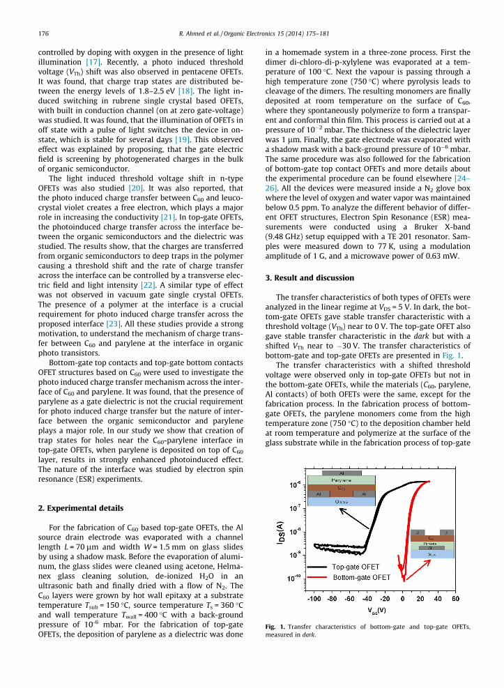
Fig. 1. Transfer characteristics of bottom-gate and top-gate OFETs,measured in dark.
2. Experimental details
For the fabrication of C60 based top-gate OFETs, the Alsource drain electrode was evaporated with a channellength L = 70 lm and width W = 1.5 mm on glass slidesby using a shadow mask. Before the evaporation of alumi-num, the glass slides were cleaned using acetone, Helma-nex glass cleaning solution, de-ionized H2O in anultrasonic bath and finally dried with a flow of N2. TheC60 layers were grown by hot wall epitaxy at a substratetemperature Tsub = 150 �C, source temperature Ts = 360 �Cand wall temperature Twall = 400 �C with a back-groundpressure of 10-6 mbar. For the fabrication of top-gateOFETs, the deposition of parylene as a dielectric was done
in a homemade system in a three-zone process. First thedimer di-chloro-di-p-xylylene was evaporated at a tem-perature of 100 �C. Next the vapour is passing through ahigh temperature zone (750 �C) where pyrolysis leads tocleavage of the dimers. The resulting monomers are finallydeposited at room temperature on the surface of C60,where they spontaneously polymerize to form a transpar-ent and conformal thin film. This process is carried out at apressure of 10�2 mbar. The thickness of the dielectric layerwas 1 lm. Finally, the gate electrode was evaporated witha shadow mask with a back-ground pressure of 10�6 mbar.The same procedure was also followed for the fabricationof bottom-gate top contact OFETs and more details aboutthe experimental procedure can be found elsewhere [24–26]. All the devices were measured inside a N2 glove boxwhere the level of oxygen and water vapor was maintainedbelow 0.5 ppm. To analyze the different behavior of differ-ent OFET structures, Electron Spin Resonance (ESR) mea-surements were conducted using a Bruker X-band(9.48 GHz) setup equipped with a TE 201 resonator. Sam-ples were measured down to 77 K, using a modulationamplitude of 1 G, and a microwave power of 0.63 mW.
3. Result and discussion
The transfer characteristics of both types of OFETs wereanalyzed in the linear regime at VDS = 5 V. In dark, the bot-tom-gate OFETs gave stable transfer characteristic with athreshold voltage (VTh) near to 0 V. The top-gate OFET alsogave stable transfer characteristic in the dark but with ashifted VTh near to �30 V. The transfer characteristics ofbottom-gate and top-gate OFETs are presented in Fig. 1.
The transfer characteristics with a shifted thresholdvoltage were observed only in top-gate OFETs but not inthe bottom-gate OFETs, while the materials (C60, parylene,Al contacts) of both OFETs were the same, except for thefabrication process. In the fabrication process of bottom-gate OFETs, the parylene monomers come from the hightemperature zone (750 �C) to the deposition chamber heldat room temperature and polymerize at the surface of theglass substrate while in the fabrication process of top-gate
R. Ahmed et al. / Organic Electronics 15 (2014) 175–181 177
OFETs, the hot parylene monomers have to crosslink at thesurface of C60. Therefore, during the deposition of paryleneon the surface of C60, there is a finite probability, that par-ylene monomers may react with C60 instead of polymerizewith each other.
3.1. Electron spin resonance
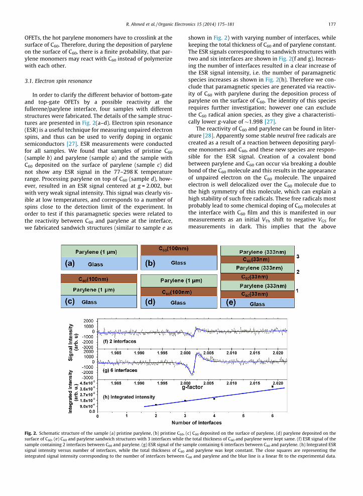
In order to clarify the different behavior of bottom-gateand top-gate OFETs by a possible reactivity at thefullerene/parylene interface, four samples with differentstructures were fabricated. The details of the sample struc-tures are presented in Fig. 2(a–d). Electron spin resonance(ESR) is a useful technique for measuring unpaired electronspins, and thus can be used to verify doping in organicsemiconductors [27]. ESR measurements were conductedfor all samples. We found that samples of pristine C60
(sample b) and parylene (sample a) and the sample withC60 deposited on the surface of parylene (sample c) didnot show any ESR signal in the 77–298 K temperaturerange. Processing parylene on top of C60 (sample d), how-ever, resulted in an ESR signal centered at g = 2.002, butwith very weak signal intensity. This signal was clearly vis-ible at low temperatures, and corresponds to a number ofspins close to the detection limit of the experiment. Inorder to test if this paramagnetic species were related tothe reactivity between C60 and parylene at the interface,we fabricated sandwich structures (similar to sample e as
Fig. 2. Schematic structure of the sample (a) pristine parylene, (b) pristine C60, (surface of C60. (e) C60 and parylene sandwich structures with 3 interfaces while tsample containing 2 interfaces between C60 and parylene. (g) ESR signal of the sasignal intensity versus number of interfaces, while the total thickness of C60 aintegrated signal intensity corresponding to the number of interfaces between C
shown in Fig. 2) with varying number of interfaces, whilekeeping the total thickness of C60 and of parylene constant.The ESR signals corresponding to sandwich structures withtwo and six interfaces are shown in Fig. 2(f and g). Increas-ing the number of interfaces resulted in a clear increase ofthe ESR signal intensity, i.e. the number of paramagneticspecies increases as shown in Fig. 2(h). Therefore we con-clude that paramagnetic species are generated via reactiv-ity of C60 with parylene during the deposition process ofparylene on the surface of C60. The identity of this speciesrequires further investigation; however one can excludethe C60 radical anion species, as they give a characteristi-cally lower g-value of �1.998 [27].
The reactivity of C60 and parylene can be found in liter-ature [28]. Apparently some stable neutral free radicals arecreated as a result of a reaction between depositing paryl-ene monomers and C60, and these new species are respon-sible for the ESR signal. Creation of a covalent bondbetween parylene and C60 can occur via breaking a doublebond of the C60 molecule and this results in the appearanceof unpaired electron on the C60 molecule. The unpairedelectron is well delocalized over the C60 molecule due tothe high symmetry of this molecule, which can explain ahigh stability of such free radicals. These free radicals mostprobably lead to some chemical doping of C60 molecules atthe interface with C60 film and this is manifested in ourmeasurements as an initial VTh shift to negative VGS formeasurements in dark. This implies that the above
c) C60 deposited on the surface of parylene, (d) parylene deposited on thehe total thickness of C60 and parylene were kept same. (f) ESR signal of themple containing 6 interfaces between C60 and parylene. (h) Integrated ESRnd parylene was kept constant. The close squares are representing the60 and parylene and the blue line is a linear fit to the experimental data.
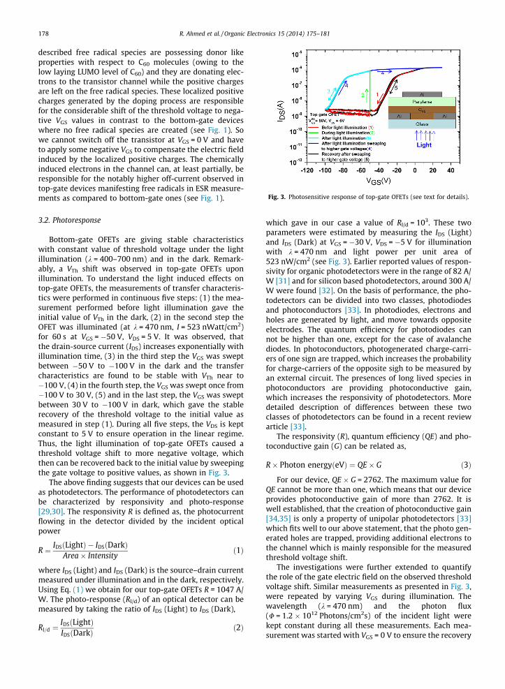
Fig. 3. Photosensitive response of top-gate OFETs (see text for details).
178 R. Ahmed et al. / Organic Electronics 15 (2014) 175–181
described free radical species are possessing donor likeproperties with respect to C60 molecules (owing to thelow laying LUMO level of C60) and they are donating elec-trons to the transistor channel while the positive chargesare left on the free radical species. These localized positivecharges generated by the doping process are responsiblefor the considerable shift of the threshold voltage to nega-tive VGS values in contrast to the bottom-gate deviceswhere no free radical species are created (see Fig. 1). Sowe cannot switch off the transistor at VGS = 0 V and haveto apply some negative VGS to compensate the electric fieldinduced by the localized positive charges. The chemicallyinduced electrons in the channel can, at least partially, beresponsible for the notably higher off-current observed intop-gate devices manifesting free radicals in ESR measure-ments as compared to bottom-gate ones (see Fig. 1).
3.2. Photoresponse
Bottom-gate OFETs are giving stable characteristicswith constant value of threshold voltage under the lightillumination (k = 400–700 nm) and in the dark. Remark-ably, a VTh shift was observed in top-gate OFETs uponillumination. To understand the light induced effects ontop-gate OFETs, the measurements of transfer characteris-tics were performed in continuous five steps: (1) the mea-surement performed before light illumination gave theinitial value of VTh in the dark, (2) in the second step theOFET was illuminated (at k = 470 nm, I = 523 nWatt/cm2)for 60 s at VGS = �50 V, VDS = 5 V. It was observed, thatthe drain-source current (IDS) increases exponentially withillumination time, (3) in the third step the VGS was sweptbetween �50 V to �100 V in the dark and the transfercharacteristics are found to be stable with VTh near to�100 V, (4) in the fourth step, the VGS was swept once from�100 V to 30 V, (5) and in the last step, the VGS was sweptbetween 30 V to �100 V in dark, which gave the stablerecovery of the threshold voltage to the initial value asmeasured in step (1). During all five steps, the VDS is keptconstant to 5 V to ensure operation in the linear regime.Thus, the light illumination of top-gate OFETs caused athreshold voltage shift to more negative voltage, whichthen can be recovered back to the initial value by sweepingthe gate voltage to positive values, as shown in Fig. 3.
The above finding suggests that our devices can be usedas photodetectors. The performance of photodetectors canbe characterized by responsivity and photo-response[29,30]. The responsivity R is defined as, the photocurrentflowing in the detector divided by the incident opticalpower
R ¼ IDSðLightÞ � IDSðDarkÞArea� Intensity
ð1Þ
where IDS (Light) and IDS (Dark) is the source–drain currentmeasured under illumination and in the dark, respectively.Using Eq. (1) we obtain for our top-gate OFETs R = 1047 A/W. The photo-response (Rl/d) of an optical detector can bemeasured by taking the ratio of IDS (Light) to IDS (Dark),
Rl=d ¼IDSðLightÞIDSðDarkÞ ð2Þ
which gave in our case a value of Rl/d = 103. These twoparameters were estimated by measuring the IDS (Light)and IDS (Dark) at VGS = �30 V, VDS = �5 V for illuminationwith k = 470 nm and light power per unit area of523 nW/cm2 (see Fig. 3). Earlier reported values of respon-sivity for organic photodetectors were in the range of 82 A/W [31] and for silicon based photodetectors, around 300 A/W were found [32]. On the basis of performance, the pho-todetectors can be divided into two classes, photodiodesand photoconductors [33]. In photodiodes, electrons andholes are generated by light, and move towards oppositeelectrodes. The quantum efficiency for photodiodes cannot be higher than one, except for the case of avalanchediodes. In photoconductors, photogenerated charge-carri-ers of one sign are trapped, which increases the probabilityfor charge-carriers of the opposite sigh to be measured byan external circuit. The presences of long lived species inphotoconductors are providing photoconductive gain,which increases the responsivity of photodetectors. Moredetailed description of differences between these twoclasses of photodetectors can be found in a recent reviewarticle [33].
The responsivity (R), quantum efficiency (QE) and pho-toconductive gain (G) can be related as,
R� Photon energyðeVÞ ¼ QE� G ð3Þ
For our device, QE � G = 2762. The maximum value forQE cannot be more than one, which means that our deviceprovides photoconductive gain of more than 2762. It iswell established, that the creation of photoconductive gain[34,35] is only a property of unipolar photodetectors [33]which fits well to our above statement, that the photo gen-erated holes are trapped, providing additional electrons tothe channel which is mainly responsible for the measuredthreshold voltage shift.
The investigations were further extended to quantifythe role of the gate electric field on the observed thresholdvoltage shift. Similar measurements as presented in Fig. 3,were repeated by varying VGS during illumination. Thewavelength (k = 470 nm) and the photon flux(U = 1.2 � 1012 Photons/cm2s) of the incident light werekept constant during all these measurements. Each mea-surement was started with VGS = 0 V to ensure the recovery
R. Ahmed et al. / Organic Electronics 15 (2014) 175–181 179
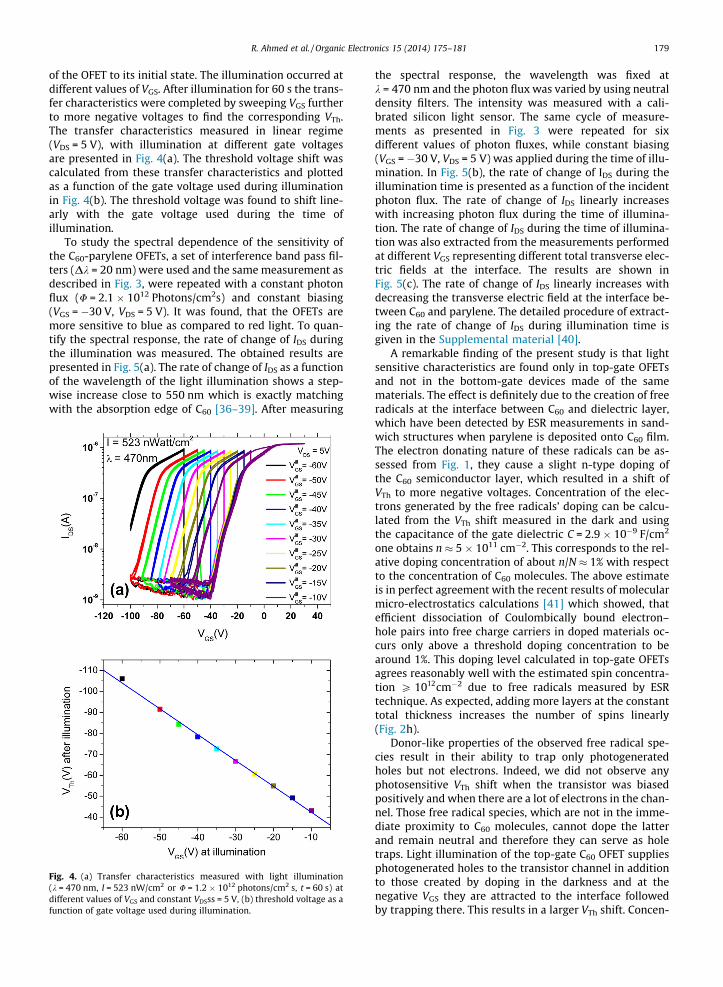
of the OFET to its initial state. The illumination occurred atdifferent values of VGS. After illumination for 60 s the trans-fer characteristics were completed by sweeping VGS furtherto more negative voltages to find the corresponding VTh.The transfer characteristics measured in linear regime(VDS = 5 V), with illumination at different gate voltagesare presented in Fig. 4(a). The threshold voltage shift wascalculated from these transfer characteristics and plottedas a function of the gate voltage used during illuminationin Fig. 4(b). The threshold voltage was found to shift line-arly with the gate voltage used during the time ofillumination.
To study the spectral dependence of the sensitivity ofthe C60-parylene OFETs, a set of interference band pass fil-ters (Dk = 20 nm) were used and the same measurement asdescribed in Fig. 3, were repeated with a constant photonflux (U = 2.1 � 1012 Photons/cm2s) and constant biasing(VGS = �30 V, VDS = 5 V). It was found, that the OFETs aremore sensitive to blue as compared to red light. To quan-tify the spectral response, the rate of change of IDS duringthe illumination was measured. The obtained results arepresented in Fig. 5(a). The rate of change of IDS as a functionof the wavelength of the light illumination shows a step-wise increase close to 550 nm which is exactly matchingwith the absorption edge of C60 [36–39]. After measuring
Fig. 4. (a) Transfer characteristics measured with light illumination(k = 470 nm, I = 523 nW/cm2 or U = 1.2 � 1012 photons/cm2 s, t = 60 s) atdifferent values of VGS and constant VDSss = 5 V, (b) threshold voltage as afunction of gate voltage used during illumination.
the spectral response, the wavelength was fixed atk = 470 nm and the photon flux was varied by using neutraldensity filters. The intensity was measured with a cali-brated silicon light sensor. The same cycle of measure-ments as presented in Fig. 3 were repeated for sixdifferent values of photon fluxes, while constant biasing(VGS = �30 V, VDS = 5 V) was applied during the time of illu-mination. In Fig. 5(b), the rate of change of IDS during theillumination time is presented as a function of the incidentphoton flux. The rate of change of IDS linearly increaseswith increasing photon flux during the time of illumina-tion. The rate of change of IDS during the time of illumina-tion was also extracted from the measurements performedat different VGS representing different total transverse elec-tric fields at the interface. The results are shown inFig. 5(c). The rate of change of IDS linearly increases withdecreasing the transverse electric field at the interface be-tween C60 and parylene. The detailed procedure of extract-ing the rate of change of IDS during illumination time isgiven in the Supplemental material [40].
A remarkable finding of the present study is that lightsensitive characteristics are found only in top-gate OFETsand not in the bottom-gate devices made of the samematerials. The effect is definitely due to the creation of freeradicals at the interface between C60 and dielectric layer,which have been detected by ESR measurements in sand-wich structures when parylene is deposited onto C60 film.The electron donating nature of these radicals can be as-sessed from Fig. 1, they cause a slight n-type doping ofthe C60 semiconductor layer, which resulted in a shift ofVTh to more negative voltages. Concentration of the elec-trons generated by the free radicals’ doping can be calcu-lated from the VTh shift measured in the dark and usingthe capacitance of the gate dielectric C = 2.9 � 10�9 F/cm2
one obtains n � 5 � 1011 cm�2. This corresponds to the rel-ative doping concentration of about n/N � 1% with respectto the concentration of C60 molecules. The above estimateis in perfect agreement with the recent results of molecularmicro-electrostatics calculations [41] which showed, thatefficient dissociation of Coulombically bound electron–hole pairs into free charge carriers in doped materials oc-curs only above a threshold doping concentration to bearound 1%. This doping level calculated in top-gate OFETsagrees reasonably well with the estimated spin concentra-tion P 1012cm�2 due to free radicals measured by ESRtechnique. As expected, adding more layers at the constanttotal thickness increases the number of spins linearly(Fig. 2h).
Donor-like properties of the observed free radical spe-cies result in their ability to trap only photogeneratedholes but not electrons. Indeed, we did not observe anyphotosensitive VTh shift when the transistor was biasedpositively and when there are a lot of electrons in the chan-nel. Those free radical species, which are not in the imme-diate proximity to C60 molecules, cannot dope the latterand remain neutral and therefore they can serve as holetraps. Light illumination of the top-gate C60 OFET suppliesphotogenerated holes to the transistor channel in additionto those created by doping in the darkness and at thenegative VGS they are attracted to the interface followedby trapping there. This results in a larger VTh shift. Concen-
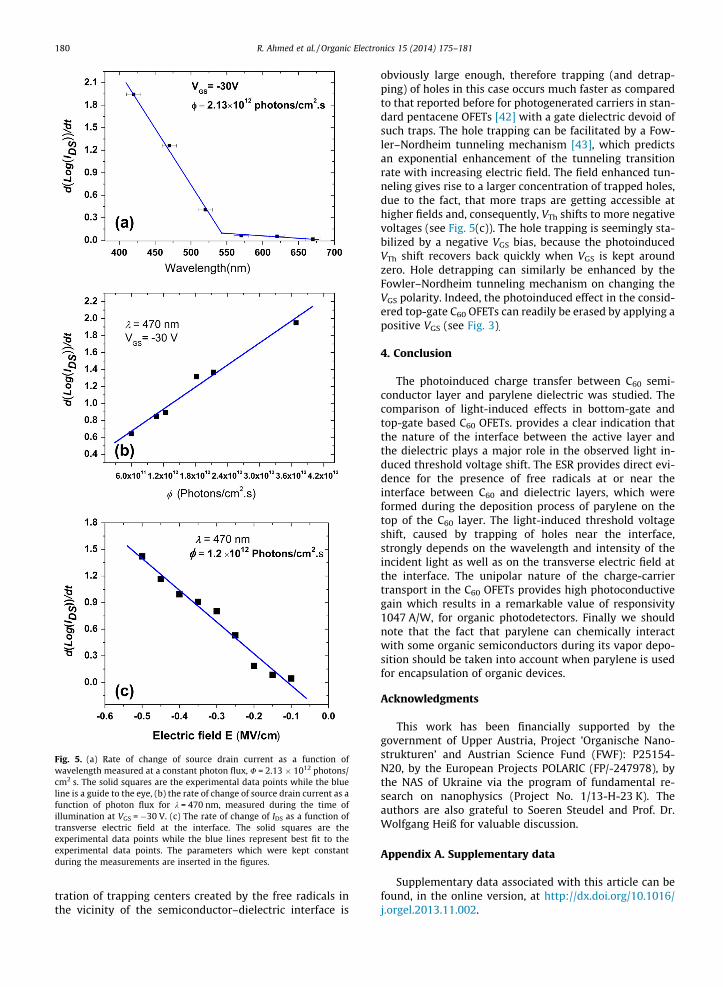
Fig. 5. (a) Rate of change of source drain current as a function ofwavelength measured at a constant photon flux, U = 2.13 � 1012 photons/cm2 s. The solid squares are the experimental data points while the blueline is a guide to the eye, (b) the rate of change of source drain current as afunction of photon flux for k = 470 nm, measured during the time ofillumination at VGS = �30 V. (c) The rate of change of IDS as a function oftransverse electric field at the interface. The solid squares are theexperimental data points while the blue lines represent best fit to theexperimental data points. The parameters which were kept constantduring the measurements are inserted in the figures.
180 R. Ahmed et al. / Organic Electronics 15 (2014) 175–181
tration of trapping centers created by the free radicals inthe vicinity of the semiconductor–dielectric interface is
obviously large enough, therefore trapping (and detrap-ping) of holes in this case occurs much faster as comparedto that reported before for photogenerated carriers in stan-dard pentacene OFETs [42] with a gate dielectric devoid ofsuch traps. The hole trapping can be facilitated by a Fow-ler–Nordheim tunneling mechanism [43], which predictsan exponential enhancement of the tunneling transitionrate with increasing electric field. The field enhanced tun-neling gives rise to a larger concentration of trapped holes,due to the fact, that more traps are getting accessible athigher fields and, consequently, VTh shifts to more negativevoltages (see Fig. 5(c)). The hole trapping is seemingly sta-bilized by a negative VGS bias, because the photoinducedVTh shift recovers back quickly when VGS is kept aroundzero. Hole detrapping can similarly be enhanced by theFowler–Nordheim tunneling mechanism on changing theVGS polarity. Indeed, the photoinduced effect in the consid-ered top-gate C60 OFETs can readily be erased by applying apositive VGS (see Fig. 3).
4. Conclusion
The photoinduced charge transfer between C60 semi-conductor layer and parylene dielectric was studied. Thecomparison of light-induced effects in bottom-gate andtop-gate based C60 OFETs. provides a clear indication thatthe nature of the interface between the active layer andthe dielectric plays a major role in the observed light in-duced threshold voltage shift. The ESR provides direct evi-dence for the presence of free radicals at or near theinterface between C60 and dielectric layers, which wereformed during the deposition process of parylene on thetop of the C60 layer. The light-induced threshold voltageshift, caused by trapping of holes near the interface,strongly depends on the wavelength and intensity of theincident light as well as on the transverse electric field atthe interface. The unipolar nature of the charge-carriertransport in the C60 OFETs provides high photoconductivegain which results in a remarkable value of responsivity1047 A/W, for organic photodetectors. Finally we shouldnote that the fact that parylene can chemically interactwith some organic semiconductors during its vapor depo-sition should be taken into account when parylene is usedfor encapsulation of organic devices.
Acknowledgments
This work has been financially supported by thegovernment of Upper Austria, Project ’Organische Nano-strukturen’ and Austrian Science Fund (FWF): P25154-N20, by the European Projects POLARIC (FP/-247978), bythe NAS of Ukraine via the program of fundamental re-search on nanophysics (Project No. 1/13-H-23 K). Theauthors are also grateful to Soeren Steudel and Prof. Dr.Wolfgang Heiß for valuable discussion.
Appendix A. Supplementary data
Supplementary data associated with this article can befound, in the online version, at http://dx.doi.org/10.1016/j.orgel.2013.11.002.
R. Ahmed et al. / Organic Electronics 15 (2014) 175–181 181
References
[1] H. Sirringhaus, M. Ando, MRS Bull. 33 (2008) 676.[2] S.F. Nelson, Y.Y. Lin, D.J. Gundlach, T.N. Jackson, Appl. Phys. Lett. 72
(1998) 1854.[3] I. McCulloch, M. Heeney, C. bailey, K. Genevicius, I. Macdonald, M.
Shkunov, D. Sparrowe, S. Tierney, R. Wagner, W.M. Toney, Nat.Mater. 5 (2006) 328.
[4] A. Dodabalapur, L. Torsi, H.E. Katz, Science 268 (1995) 27.[5] G. Horowitz, Adv. Mater. 10 (1998) 365.[6] H.N. Tsao, K. Müllen, Chem. Soc. Rev. 39 (2010) 2372.[7] F. Garnier, R. Hajlaoui, A. Yassar, Science 265 (1994) 1684.[8] R.A. Street, Adv. Mater. 2009 (2007) 21.[9] P.F. Baude, D.A. Ender, M.A. haase, T.W. Kelley, D.V. Muyres, S.D.
Theiss, Appl. Phys. Lett. 82 (2003) 3964.[10] R. Rotzoll, S. Mohapatra, V. Olariu, R. Wenz, M. Grigas, K. Dimmler, O.
Shchekin, A. Dodabalapur, Appl. Phys. Lett. 88 (2006) 123502.[11] N. Karl, Synth. Met. 133 (2003) 649.[12] M.Y. Cho, S.J. Kim, Y.D. Han, D.H. Park, K.H. Kim, D.H. Choi, J. Joo, Adv.
Funct. Mater. 18 (2008) 2905.[13] Q. Tang, L. Li, Y. Song, Y. Liu, H. Li, W. Xu, Y. Liu, W. Hu, D. Zhu, Adv.
Mater. 19 (2007) 2624.[14] S. Dutta, K.S. Narayan, Phys. Rev. B 68 (2003) 125208.[15] Y. Guo, C. Du, C. Di, J. Zheng, X. Sun, Y. Wen, L. Zhang, W. Wu, G. Yu,
Y. Liu, Appl. Phys. Lett. 94 (2009) 143303.[16] H. Kuroda, E.A. Flood, Can. J. Chem. 1961 (1981) 39.[17] S. Ogawa, T. Naijo, Y. Kimura, H. Ishii, M. Niwano, Appl. Phys. Lett. 86
(2005) 252104.[18] C.B. Park, Appl. Phys. Lett. 100 (2012) 063306.[19] V. Podzorov, V.M. Pudalov, M.E. Gershenson, Appl. Phys. Lett. 85
(2004) 6039.[20] M. Barra, F. Bloisi, A. Cassinese, F.V. Di Girolamo, L. Vicari, J. Appl.
Phys. 106 (2009) 126105.[21] F. Li, A. Werner, M. Pfeiffer, K. Leo, J. Phys. Chem. B 108 (2004)
17076.[22] V. Podzorov, M.E. Gershenson, Phys. Rev. Lett. 95 (2005) 016602.[23] V. Podzorov, E. Menard, A. Borissov, V. Kiryukhin, J.A. Rogers, M.E.
Gershenson, Phys. Rev. Lett. 93 (2004) 086602.
[24] A. Nigam, G. Schwabegger, M. Ullah, R. Ahmed, I.I. Fishchuk, A.Kadashchuk, C. Simbrunner, H. Sitter, M. Premaratne, V.R. Rao, Appl.Phys. Lett. 101 (2012) 083305.
[25] G. Schwabegger, M. Ullah, M. Irimia-Vladu, M. Baumgartner, Y.Kanbur, R. Ahmed, P. Stadler, S. Bauer, N.S. Sariciftci, H. Sitter, Synth.Met. 161 (2011) 2058.
[26] R. Ahmed, M. Sams, C. Simbrunner, M. Ullah, K. Rehman, G.Schwabegger, H. Sitter, T. Ostermann, Synth. Met. 161 (2012) 2562.
[27] E.D. Glowacki, K.L. Marshall, C.W. Tang, N.S. Sariciftci, Appl. Phys.Lett. 99 (2011) 043305.
[28] D.A. Loy, R.A. Assink, J. Am. Chem. Soc. 114 (1992) 3977.[29] Y.-Y. Noh, J. Ghim, S.-J. Kang, K.-J. Baeg, D.-Y. Kim, K. Yase, J. Appl.
Phys. 100 (2006) 094501.[30] Y.-Y. Noh, D.-Y. Kim, K. Yase, J. Appl. Phys. 98 (2005) 74505.[31] Y.-Y. Noh, D.-Y. Kim, Y. Yoshida, K. Yase, B.-J. Jung, E. Lim, H.-K. Shim,
Appl. Phys. Lett. 86 (2005) 043501.[32] N.M. Johnson, A. Chiang, Appl. Phys. Lett. 45 (1984) 1102.[33] G. Konstantatos, E.H. Sargent, Nat. Nanotechnol. 5 (2010) 391.[34] C.H.E.N. H-Yu, M.K.F. Lo, G. Yang, H.G. Monbouquette, Y. Yang, Nat.
Nanotechnol. 3 (2008) 543.[35] J. Reynaert, V.I. Arkhipov, P. Heremans, J. Poortmans, Adv. Funct.
Mater. 16 (2006) 784.[36] S-Z. Kang, S-L. Xu, M-J. Han, S. Lei, C. Wang, Li-J. Wan, C-Li. Bai,
Colloids and Surf. A: Physicochem. Eng. Aspects 257-258 (2005)195–198.
[37] W-Y. Zhouy, Si-S. Xiey, S-fa. Qiany, G. Wangy, Lu-xi Qianz, J. Phys.Cond. Matter. 8 (1996) 5793.
[38] H. Zhang, C. Wu1, L. Liang, Y. Chen, Y. He, Y. Zhu, N. Ke, J.B. Xu, S.P.Wong, A. Wei, S. Peng, J. Phys. Cond. Matter. 13 (2001) 2883.
[39] G.U. Gang, Z. Wencheng, Z. Hao, C. Geng, D.U. Youwei, Z. Yibin, Z.Shuyi, Chin. Phys. Lett. 11 (1994) 102.
[40] Please see supplemental material.[41] A. Mityashin, Y. Olivier, T. Van Regemorter, C. Rolin, S. Verlaak, N.
Martinelli, D. Beljonne, J. Cornil, J. Genoe, P. Heremans, Adv. Mater.24 (2012) 1535.
[42] M. Debucquoy, S. Verlaak, S. Steudel, K. Myny, J. Genoe, P. Heremans,Appl. Phys. Lett. 91 (2007) 103508.
[43] J.J. Chang, IEEE Trans. Electron Dev. ED-24 (1977) 511.