
Impedance spectroscopy and investigation of conduction mechanism in BaMnO3 nanorods
Upload
independentCategory
view
6download
0
Advanced Nanoscience and Technology: An International Journal (ANTJ), Vol. 1, No. 1, June 2014
21
OPTICAL BEHAVIOUR OF SYNTHESIZED ZNONANOTABLETS AND ITS TRANSFORMEDNANORODSWITH THE ASSISTANCE OF A
CATIONIC SURFACTANT CTAB
Pritam Saha1 and Tapas Pal Majumder1, * and Subhas Chandra Debnath2
1Department of Physics, University of Kalyani, Kalyani-741235, West Bengal, India.2Department of Chemistry, University of Kalyani, Kalyani-741235, West Bengal, India.
ABSTRACT
We are reporting the preparation of ZnO nanotablets at relatively low temperature (1500C) using zincacetate [Zn(Ac)2], NaOH, cetyltrimethylammonium bromide (CTAB) by solvothermal method. By adjustingthe molar ratio of the reactants we obtained nanorods and we also obtained the variation of the dimensionof the nanorods using hydrazine hydrate as capping reagent. The prepared samples were morphologicallyrecognized as well crystallized. The average diameter of the ZnO nanotablets were ranging from 500 to600 nm and the average thickness of the nanotablets were ranging from 85 to 90 nm. The length of ZnOnanorods were ranging from 300 to several micrometers and breadth of the ZnO nanorods were rangingfrom 80 to 160 nm. The optical properties of the prepared materials have also been studied with theexhibition of its interesting behavior.
Keywords
Nanostructures; Thin films; Sol-gel growth; X-ray diffraction; Optical properties
1. INTRODUCTION
In recent years one dimensional (1D) semiconductor nanostructures such as nanorods, nanowires,nanobelts and nanotubes have been attracted great attention due to their many unique properties.The possibility of such unique properties can be exploited for obtaining as building materials ofthe construction of future electronics and photonics devices [1-3]. 1D semiconductornanostructures also has their applications in life sciences [4]. They also have potential uses asinterconnectors, nanoscale electronics, optoelectronics and sensing devices [5]. It is generallyaccepted that 1D nanostructure are useful materials for investigating the dependence of electricaland thermal transport or mechanical properties based on dimensionality and size reduction orquantum confinement effects [6]. Zinc oxide having a wide direct band-gap (3.37 eV) with alarge excitonic binding energy of 60 meV at room temperature, has been recently attracted due totheir potential uses in ultra-violet (UV) luminescence devices, light emitting diodes (LEDs), gassensors, solar cells and transparent thin film transistors [7]. ZnO is also a material that isbiocompatible and biosafe. ZnO may be used as implantable biosensors and it also hasbiomedical applications.
Advanced Nanoscience and Technology: An International Journal (ANTJ), Vol. 1, No. 1, June 2014
22
In the past few years, much effort has been devoted to develop various 1D semiconductornanostructures [8-10]. Several researchers have developed various kinds of ZnO nanostructuressuch as nanodots, nanorods, nanowires, nanobelts, nanotubes, nanobridges and nanonails,nanowalls, nanohelixes, seamless nanorings, mesoporous single-crystal nanowires, andpolyhedral cages [11-13]. Till date various synthetic methods have been reported such as vapour–liquid-solid ( VLS ) [14-16], vapour–solid (VS) [17] mechanism, laser ablation–catalytic growth[18-19], oxide–assisted growth [20], template–induced growth [21-22], solution–liquid–solidgrowth in organic solvents [23-24], metal–organic chemical vapour deposition (MOCVD) [25],hydrothermal synthesis, the micro–emulsion hydrothermal process, chemical vapour deposition(CVD) and a catalyst–free CVD method [26-29]. They have been largely reported on thesynthesis of pure ZnO nanorods/ nanowires by solvothermal/ hydrothermal methods [30-34].Among the 1D nanostructures ZnO nanorods and nanowires have been widely studied because oftheir easy nanomaterials formation and device applications.
In this paper, we have prepared ZnO nanotablets by the assistance of the cationic surfactantcetyltrimethylammonium bromide (CTAB). We extensively studied the variation of dimensionsof ZnO nanorods by changing the reactant’s molar ratio. We also studied that the diameter andlength of the nanorods can be easily tuned by the introduction of the capping reagent hydrazinehydrate. The optical properties of the as prepared materials have been studied extensively forelaborating their comparable band gaps and photoluminescence behavior.
2. EXPERIMENTAL SECTION
All the reactants, purchased from E-Merck Germany, were of analytical grade and were usedwithout any further purification.
a) Preparation of ZnO nanostructures
In a typical procedure to synthesize ZnO nanostructure, 6.00gm of Zinc acetate (Zn(Ac)2) was putinto a glass beaker filled with 15ml of double distilled water. The mixture was stirred for 10minutes at room temperature to form a solution. Following the same procedure we make anothersolution putting 0.3 gm of CTAB into 10 ml of double distilled water. Then the solution of CTABwas added into the glass beaker containing the Zn(AC)2 solution and left for 15 minutes undervigorous stirring for proper mixing of the two solutions. Then we added drop wise the as prepared15 ml of 4M NaOH solution into the glass beaker during vigorous stirring and left for another 15minutes under that vigorous stirring. The colour of the solution was white .Then the solution wasput into a Teflon lined stainless steel autoclave. The autoclave was maintained at average 1200Cfor 24 hours, and then allowed to naturally cool to room temperature. The resulting whiteprecipitate was filtered, subsequently washed with double distilled water and absolute ethanol anddried in air at 650C for 3 hours. We get nanotablets. This is the first experiment (i.e., ZnO 1) toobtain ZnO nanotablets. To change the shape of the nanostructure we repeated the sameexperiment with different molar ratio of the reactants and CTAB also and we got nanorods. Nowto change the dimension of the nanorods we used hydrazine hydrate as a capping reagent in thesame experiment keeping the other reactant’s molar ratio constant and at the same reactionconditions. The detailed information about other experiments is given in Table no. 1.

Advanced Nanoscience and Technology: An International Journal (ANTJ), Vol. 1, No. 1, June 2014
23
Table 1 Summary of Experimental Conditions and the Morphology of Different ZnO Nanostructures.
ExperimentNo.
Nanostructures and energy band gap Zn(Ac)2 NaOH Solution CTAB Capping Reagent (Hydrazine hydrate) Temperature Time Duration
1 (ZnO 1) Nanotablets2.6 eV
6 gm 15 ml 4M 0.3 gm N i l 1 2 0 0 C 24 hr.
2 (ZnO 2) Nanorods2.8 eV
7 gm 30 ml 5M 0.5 gm N i l 1 2 5 0 C 24 hr.
3 (ZnO 3) Nanorods2.6 eV
7 gm 40 ml 5M 0.5 gm 1 0 m l 1 2 5 0 C 24 hr.
4 (ZnO 4) Nanorods2.2 eV
7 gm 50 ml 5M 0.5 gm 2 0 m l 1 2 5 0 C 24 hr.
b) Characterization
Crystalline structure of the obtained products were characterised by X-ray diffraction studies(XRD) using a diffractometer (Bruker D8 Advance) with CuKα line. The morphology of theseproducts was obtained by field emission scanning electron microscopy (FE-SEM) and the FE-SEM photos were taken with a S4800-JU at 5.0 kV. The FE-SEM measurements were done onthe glass substrate coated with requisite samples using a programmable Spin Coater, ApexInstruments Co. with model No.SCU-2008 C. UV-vis spectrophotometer (Model: TCC-240A,UV-2401 PC, Shimadzu, Japan) was used to record the electronic absorption spectra of theobtained products at room temperature. Photoluminescence spectra were carried out on a LS55,Fluorescence spectrometer, PerkinElmer using excitation source of the 300 nm and 500 nm lineof a He-Cd laser.
3. RESULTS AND DISCUSSION
a) Crystalline structure and Morphology
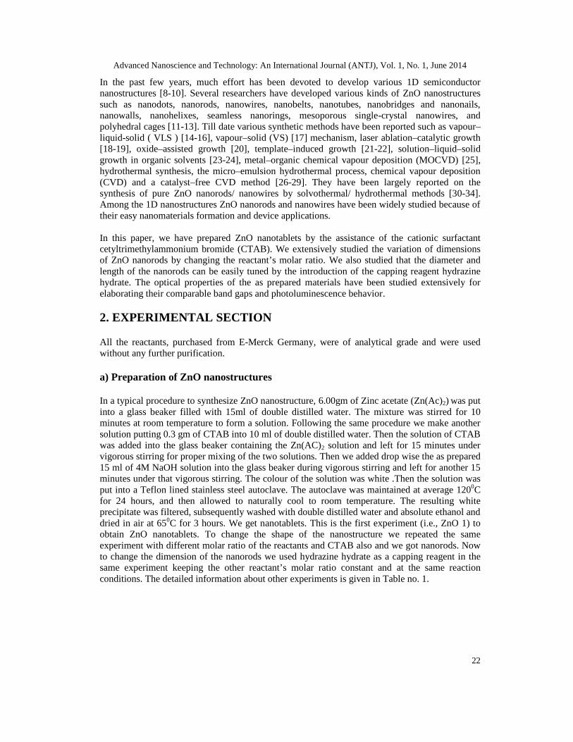
The structure and size of the ZnO nanostructures can easily be seen by the low and highmagnification of FESEM images shown in Fig. 1 (a – h). The average thickness of the nanotabletsis about 90 nm and the thickness is ranging on average from 85 to 95 nm. The average diameterof the nanotablets is ranging from 500 to 600 nm. The nanotablets are almost uniform in shapeand size. The shape of the nanorods is straight. The length of the nanorods is ranging from 300nm to several micrometers and the diameter of the nanorods is ranging from 80 to 160 nm.
Advanced Nanoscience and Technology: An International Journal (ANTJ), Vol. 1, No. 1, June 2014
24
Fig. 1 FESEM micrograph of different types of ZnO nanostructures. a nanotablets (ZnO 1) with 100 nmresolution, b nanotablets (ZnO 1) with 1 µm resolution, c nanorods (ZnO 2) with 100 nm resolution, d
nanorods (ZnO 2) with 1 µm resolution, e nanorods (ZnO 3) with 100 nm resolution, f nanorods (ZnO 3)with 1 µm resolution, g nanorods (ZnO 4) with 100 nm resolution and h nanorods (ZnO 4) with 1 µm
resolution.
Advanced Nanoscience and Technology: An International Journal (ANTJ), Vol. 1, No. 1, June 2014
25
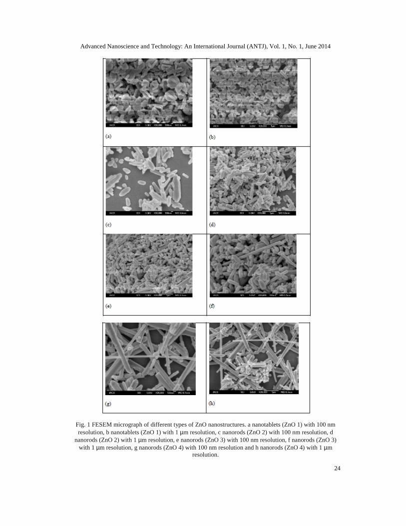
The crystal structure and crystallinity of the as prepared products were investigated by XRD. Fig2(a - d) shows a typical XRD pattern of ZnO precursors, in which all the diffraction peaks can bewell indexed to the hexagonal wurtzite ZnO crystal with lattice constant a =3.249 Å and c =5.208 Å, in good agreement with the standard PDF data (JCPDS file 36–1451). No additionalreflections are observed which indicates that there are no additional crystalline structures presentin the samples. The strong and sharp diffraction peaks demonstrate that the products are wellcrystalline. The XRD patterns of ZnO samples show the characteristic hexagonal wurtzite planesat (100), (101), (002), (102), (110), (103), (200), (112), (201), and (202) and those are located at31.730, 34.350, 36.220, 47.520, 56.610, 62.860, 66.350, 67.890, 69.090, and 76.870 in the 2 thetarange graph from 200 to 800 (Fig. 2(a-d)). In addition, the intense and sharp diffraction peaks areobserved at (100), (002), (101) etc (hkl) planes. Fig 2(a – c) suggest that the obtained products arewell crystallized. By using the XRD analysis, the d-spacing of the ZnO annotablets and nanorodshave been calculated for the hexagonal wurtzite structures and compared with the standardJCPDS data (Table 2). In our exprriment for XRD analysis, CuKα (λ=1.5418 A) radiation is usedwhereas in case of JCPDS (36 – 1451), CuKα 1 (λ=1.5405981 A) radiation was used. Moreover,the Debye-Scherrer Equation is given below as:
d=0.9*λ/β cosθ ............ ...........(1)
where ‘d’ is the breadth of the nanorods, λ= wavelength of the CuKα radiation (i.e. λ=1.5418 A),β=FWHM (Full Width Half Maxima) of the XRD peaks, θ= the angle at which the correspondingpeaks occur. By using Debye- Scherrer equation (Eqn(1)) we calculated the average thickness ofthe nanotablets and average breadth of the nanorods. The average thickness of the ZnOnanotablets (ZnO 1) is 92 nm and we get the following values of breadths of the as prepared ZnOnanorod products, those are 90 nm for ZnO 2, 93 nm for ZnO 3, and 110 nm for ZnO 4.
Advanced Nanoscience and Technology: An International Journal (ANTJ), Vol. 1, No. 1, June 2014
26
(a)(b)
(c)(d)
Fig. 2 XRD diffraction pattern of different types of ZnO nanostructures. a nanotablets (ZnO 1), b nanorods(ZnO 2), c nanorods (ZnO 3) and d nanorods (ZnO 4).
Table 2 The comparison of d-values, obtained from XRD and JCPDS, and illustration of the corresponding(h k l) values.
Peak 2θ d-XRD(Å) d-JCPDS(Å) (hkl)1 31.73 2.8199 2.8143 1002 34.35 2.6106 2.6033 0023 36.22 2.4800 2.4759 1014 47.52 1.9133 1.9111 1025 56.61 1.6258 1.6247 1106 62.86 1.4783 1.4771 1037 66.35 1.4088 1.4071 2008 67.89 1.3805 1.3781 1129 69.09 1.3594 1.3582 20110 76.87 1.2401 1.2380 202
Advanced Nanoscience and Technology: An International Journal (ANTJ), Vol. 1, No. 1, June 2014
27
b) Optical Properties
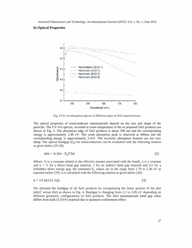
Fig. 3 UV-vis absorption spectra of different types of ZnO nanostructures.
The optical properties of semiconductor nanomaterials depend on the size and shape of theparticles. The UV-Vis spectra, recorded at room temperature of the as prepared ZnO products areshown in Fig. 3. The absorption edge of ZnO products is about 500 nm and the correspondingenergy is approximately 2.48 eV. The weak absorption peak is observed at 400nm and thecorresponding energy is approximately 3.1eV. The excitonic absorption features are not verysharp. The optical bandgap (Eg) for semiconductors can be evaluated with the following relationas given below [35-36].
αhν = A (hν - Eg)n/hν (2)
Where, A is a constant related to the effective masses associated with the bands, n is a constantand n = ½ for a direct band gap material, 2 for an indirect band gap material and 3/2 for aforbidden direct energy gap, the estimated Eg values are in the range from 1.70 to 2.30 eV asreported earlier [19]. α is calculated with the following relation as given below [20]:
α = 1/t ln(1/(1-A)) (3)
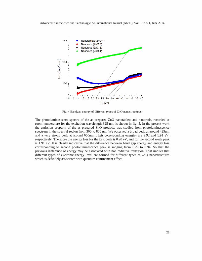
We obtained the bandgap of all ZnO products by extrapolating the linear portion of the plot(αhν)2 versus (hν) as shown in Fig. 4. Bandgap is changing from 2.2 to 2.85 eV depending ondifferent geometric configurations of ZnO products. The ZnO nanomaterials band gap valuediffers from bulk (3.37eV) material due to quantum confinement effect.
Advanced Nanoscience and Technology: An International Journal (ANTJ), Vol. 1, No. 1, June 2014
28
Fig. 4 Bandgap energy of different types of ZnO nanostructures.
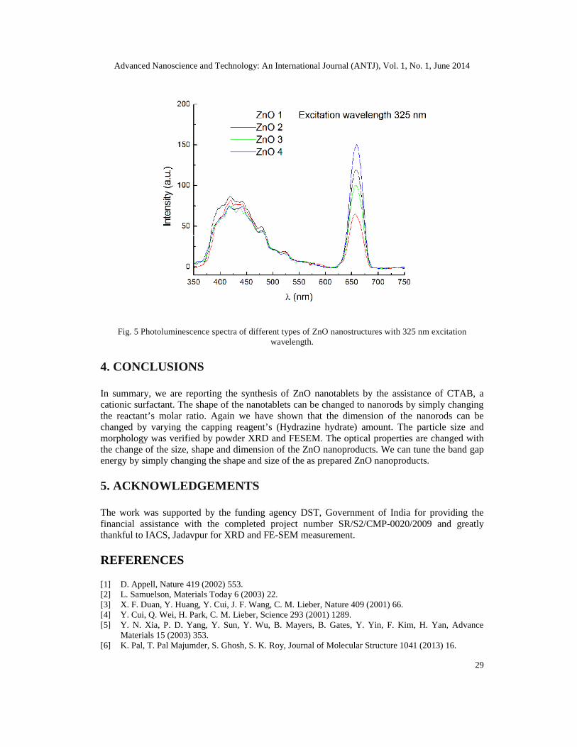
The photoluminescence spectra of the as prepared ZnO nanotablets and nanorods, recorded atroom temperature for the excitation wavelength 325 nm, is shown in fig. 5. In the present workthe emission property of the as prepared ZnO products was studied from photoluminescencespectrum in the spectral region from 300 to 800 nm. We observed a broad peak at around 425nmand a very strong peak at around 650nm. Their corresponding energies are 2.92 and 1.91 eV,respectively. Therefore the energy loss for the first peak is 0.90 eV, and for the second weak peakis 1.91 eV. It is clearly indicative that the difference between band gap energy and energy losscorresponding to second photoluminescence peak is ranging from 0.29 to 0.94. So that theprevious difference of energy may be associated with non radiative transition. That implies thatdifferent types of excitonic energy level are formed for different types of ZnO nanostructureswhich is definitely associated with quantum confinement effect.
Advanced Nanoscience and Technology: An International Journal (ANTJ), Vol. 1, No. 1, June 2014
29
Fig. 5 Photoluminescence spectra of different types of ZnO nanostructures with 325 nm excitationwavelength.
4. CONCLUSIONS
In summary, we are reporting the synthesis of ZnO nanotablets by the assistance of CTAB, acationic surfactant. The shape of the nanotablets can be changed to nanorods by simply changingthe reactant’s molar ratio. Again we have shown that the dimension of the nanorods can bechanged by varying the capping reagent’s (Hydrazine hydrate) amount. The particle size andmorphology was verified by powder XRD and FESEM. The optical properties are changed withthe change of the size, shape and dimension of the ZnO nanoproducts. We can tune the band gapenergy by simply changing the shape and size of the as prepared ZnO nanoproducts.
5. ACKNOWLEDGEMENTS
The work was supported by the funding agency DST, Government of India for providing thefinancial assistance with the completed project number SR/S2/CMP-0020/2009 and greatlythankful to IACS, Jadavpur for XRD and FE-SEM measurement.
REFERENCES
[1] D. Appell, Nature 419 (2002) 553.[2] L. Samuelson, Materials Today 6 (2003) 22.[3] X. F. Duan, Y. Huang, Y. Cui, J. F. Wang, C. M. Lieber, Nature 409 (2001) 66.[4] Y. Cui, Q. Wei, H. Park, C. M. Lieber, Science 293 (2001) 1289.[5] Y. N. Xia, P. D. Yang, Y. Sun, Y. Wu, B. Mayers, B. Gates, Y. Yin, F. Kim, H. Yan, Advance
Materials 15 (2003) 353.[6] K. Pal, T. Pal Majumder, S. Ghosh, S. K. Roy, Journal of Molecular Structure 1041 (2013) 16.
Advanced Nanoscience and Technology: An International Journal (ANTJ), Vol. 1, No. 1, June 2014
30
[7] Ü Özgür, Y. I. Alivov, C. Liu, A. Teke, M. A. Reshchikov, S. DÕgan, V. Avrutin, S. J. Cho, H.Morkoc, Journal of Applied Physics 98 (2005) 041301.
[8] P. D. Yang, C. M. Lieber, Science 273 (1996) 1836.[9] A. M. Morales, C. M. Lieber, Science 279 (1998) 208.[10] X. G. Peng, J. Wickham, A. P. Alivisatos, Journal of American Chemical Society 120 (1998) 5343.[11] Z. L. Wang, Materials Today 7 (2004) 26.[12] J. H. Park, H. J. Choi, Y. J. Choi, S. H. Sohn, J. G. Park, Journal of Materials Chemistry 14 (2004)
35.[13] J. H. Park, H. J. Choi, J. G. Park, Journal of Crystal Growth 263 (2004) 237.[14] R. S. Wagner, W. C. Ellis, Applied Physics Letters 4 (1964) 89.[15] A. I. Klimovskaya, I. P. Ostrovskii, A. S. Ostrovskaya, Physica Status Solidi A 153 (1996) 465.[16] O. Toshio, N. Masayuki, Journal of Crystal Growth 46 (1979) 504.[17] Y. Iwao, S. J. Hajime, Journal of Crystal Growth 45 (1978) 511.[18] D. P. Yu, X. S. Sun, C. S. Lee, I. Bello, S. T. Lee, H. D. Gu, K. M. Leung, G. W. Zhou, Z. F. Dong,
Z. Zhang, Applied Physics Letters 72 (1998) 1966.[19] X. F. Duan, C. M. Lieber, Journal of American Chemical Society 122 (2000) 188.[20] R. Q. Zhang, Y. Lifshitz, S. T. Lee, Advance Materials 15 (2003) 635.[21] W. Q. Han, S. S. Fan, Q. Q. Li, Y. D. Hu, Science 277 (1997) 1287.[22] C. R. Wang, K. B. Tang, Q. Yang, B. Hai, G. Z. Shen, C. H. An, W. C. Yu, Y. T. Qian, Inorganic
Chemical Communication 4 (2001) 339.[23] Y. Jiang, Y. Wu, X. Mo, W. C. Yu, Y. Xie, Y. T. Qian, Inorganic Chemistry 39 (2000) 2964.[24] C. R. Wang, K. B. Tang, Q. Yang, Y. T. Qian, Journal of Electrochemical Society 150 (2003) G163.[25] M. Yazawa, M. Koguchi, A. Muto, M. Ozawa, K. Hiruma, Applied Physics Letters 61 (1992) 2051.[26] C. L. Jiang, W. Q. Zhang, G. F. Zou, W. C. Yu, Y. T. Qian, Journal of Physical Chemistry B 109
(2005) 1361.[27] X. M. Sun, X. Chen, Z. X. Deng, Y. D. Li, Materials Chemistry and Physics A 78 (2003) 99.[28] J. J. Wu, S. C. Liu, Advance Materials 14 (2002) 215.[29] J. J. Wu, S. C. Liu, Journal of Physical Chemistry B 106 (2002) 9546.[30] J. Q. Xu, Y. P. Chen, J. N. Shen, Journal of Nanoscience Nanotechnology 6 (2006) 248.[31] Y. Zhang, J. Q. Xu, Q. Xiang, H. Li, Q. Y. Pan, P. C. Xu, Journal of Physical Chemistry C 113 (2009)
3430.[32] L. Vayssieres, Advance Materials 15 (2003) 464.[33] J. X. Wang, X. W. Sun, Y. Yang, H. Huang, Y. C. Lee, O. K. Tan, L. Vayssieres, Nanotechnology 17
(2006) 4995.[34] L. E. Greene, M. Law, J. Goldberger, F. Kim, J. C. Johnson, Y. F. Zhang, R. J. Saykally, P. D. Yang,
Angew Chemistry International 115 (2003) 3031.[35] R. B. Kale, C. D. Lokhande, Semiconductor Science and Technology 20 (2005) 1.[36] K. Pal, U. N. Maiti, T. Pal Majumder, P. Dash, N. C. Mishra, N. Bennis, J. M. Otón, Journal of
Molecular Liquids 164 (2011) 233.
Copyright © 2022 FDOKUMEN