
The Impact of Cefr-Aligned Curriculum on Year2 Intermediate ...

Hindawi Publishing CorporationJournal of NanomaterialsVolume 2013, Article ID 861017, 8 pageshttp://dx.doi.org/10.1155/2013/861017
Research ArticleRobust Nanogenerator Based on Vertically Aligned ZnONanorods Using Copper Substrate
Naveed Sheikh,1 Nitin Afzulpurkar,1 and Muhammad Waseem Ashraf2
1 School of Engineering and Technology, Asian Institute of Technology (AIT), Pathumthani, Bangkok 12120, Thailand2Department of Physics (Electronics), GC University, Lahore 54000, Pakistan
Correspondence should be addressed to Naveed Sheikh; [email protected]
Received 19 April 2013; Accepted 29 July 2013
Academic Editor: Yangchuan Xing
Copyright © 2013 Naveed Sheikh et al. This is an open access article distributed under the Creative Commons Attribution License,which permits unrestricted use, distribution, and reproduction in any medium, provided the original work is properly cited.
We report the growth of well-aligned ZnO nanorods that were successfully synthesized on copper (Cu) substrate by using a simplehydrothermal method at low temperature leading to a robust large area nanogenerator (NG) based on cost effective Cu electrodewhich could enable energy harvest from the walking motions. First, the seed layer of gold (Au) has been deposited by plasmasputtering. Then, the growth process of nanorods was carried out in a sealed chemical bath. The lengths of nanorods 5-6 𝜇m wereachieved. The longer and bigger nanorods produced a surface with larger contact area and higher roughness. The larger contactarea improves the absorption rate of incident light and the rougher surface strengthens the scattering effect. The surfaces werecharacterized by X-ray diffraction (XRD), scanning electron microscope (SEM), and energy dispersive X-ray spectroscopy (EDX).Then, Cu substrate was used for the development of high-output NG. Twenty-seven NGs were developed with maximum outputvoltage that exceeded to 1.8 V andmaximum output current that exceeded to 148 nA.The structural simulation of nanorod has alsobeen performed in ANSYS.TheCu substrate-based NG provides a feasible technique for effectively convertingmechanical energiesto electrical energy from external force.
1. Introduction
Nano structured materials have received extensive attentionfrom researchers in the last few years because of theirnovel properties which differ from those of bulk materials[1, 2]. Nanocrystalline materials exhibit completely differentproperties due to their enhanced surface to volume ratioand quantum confinement effects. Zinc oxide (ZnO) isone of the important materials and photonic material thatattracts much attention for nanodevice applications suchas nanogenerators, biomedical devices, sensors, transduc-ers, and optoelectronics because of its direct bandgap of(3.37 eV) and large exciton binding energy (60meV) atroom temperature. ZnO can be made highly conductive bydoping and transparent to visible light. Several reports onthe characterization of unidimensional nanorods of com-pound and elemental semiconductors such as GaAs [3], Ge[4], Si [5], and ZnO [6–8] are available in the literature.Currently, there is an increasing interest in the fabricationof ZnO with the various morphology and uniform size,
including low-dimensional ZnO nanostructures such asnanowires, nanosheets, nanoflowers, nanotubes, nanorods,nanocombs, nanorings, nanobelts, nanohelices, nanobows,and nanocages, which have been successfully synthesized bydifferent approaches such as thermal evaporation method,microwave heating, nonaqueous approaches, chemical vapordeposition (CVD), sol-gel process, hydrothermal process, gascondensation, laser ablation, template-assisted growth, andrefluxing method [9, 10]. One of the most inexpensive andenergy-efficient strategies for synthesizing ZnO nanorods isthe hydrothermal process which does not require complexvacuumenvironment or high temperature.Thehydrothermalprocess induces anisotropic crystal growth in a solution [11,12].The hydrothermal process provides good control over themorphology of the nanorods grown [13].The growths of ZnOnanorods on the flat substrates such as Si [13, 14] glass [15],and carbon cloth [16, 17] have been reported. However, therehave been no reports of ZnO nanorods grown on Copper(Cu) substrate. The ZnO crystal is hexagonal wurtzite withlattice parameters 𝑎 = 0.3296 nm and 𝑐 = 0.52065 nm.

2 Journal of Nanomaterials
The ZnO structure can be described as series of alternatingplanes composed of tetrahedrally coordinated (O2−) and(Zn2+) arranged along the 𝑐-axis. The basal plane (001) is themost common polar surface. One end of the basal polar planeterminates in partially negative oxygen lattice points and theother end is terminated in partially positive Zn lattice points.
The idea of human motion-based energy scavenginghas enormous technological interest in accordance withthe emergent potential of portable smart electronics [18].It is becoming more realistic, due to advanced researchin nanoelectronics, to run these devices at tremendouslylow power consumption, so that energy harvested fromthe environment may be adequate to meet the operationalmode energy needs [19]. Thermal and solar energy arethe most common and practical sources of energy to beharvested from our surroundings. However, these forms ofenergy are time and local dependent. With the advancesin technology developed for small-scale energy harvesting,it may be possible to scale up this type of technology ata large scope such as with ocean waves and wind power.Such potential needs to be explored with the considerationof the scalability of the technology, the cost of materialsand fabrication process, environmental impact, and practicalfeasibility for implementation [20]. Mechanical energy is oneof the most representative sources that can be artificiallygenerated from vibration, movement of automobile, andhuman walking, all of which are usually wasted [21]. Thefundamental mechanism of a nanogenerator (NG) is relatedto a piezoelectric potential generated in nanorods when theyare dynamically strained under an external force, and thecorresponding transient current that flows to balance theFermi levels at two contacts [22, 23].TheNG is still difficult toapply to energy harvesting device to harvest the mechanicalenergy from the environment owing to weak durability, highcost, and low-throughout process. Thus, it is necessary todevelop strategies towards achieving robust and cost-effectiveNG in order to consistently scavenge the mechanical energyfrom the environmental sources.
Huang et al. [24] reported ZnO nanorod arrays thinfilm bilayer structure for homojunction diode and high-performancememristor to complementary 1D1R application.Faisal et al. presented synthesis, characterizations, photocat-alytic, and sensing studies of ZnOnanocapsules [25]. Faisal etal. reported fabrication of ZnO nanoparticles based on sen-sitive methanol sensor and efficient photocatalyst [26]. Dinget al. presented the growing of vertical ZnO nanorod arrayswithin graphite [27]. Wrobel et al. reported direct synthesisof ZnO nanorod field emitters on metal electrodes [28]. Liuet al. studied fabrication of ZnO/CdS/Cu
2ZnSnS
4p-n het-
erostructure nanorod arrays via a solution-based route [29].Chen et al. reported synthesis of grapheme ZnO nanorodnanocomposites with improved photoactivity and antiphoto-corrosion [30]. Umar et al. reported ultrasensitive cholesterolbiosensor based on low-temperature grown ZnO nanoparti-cles [31]. Hu et al. presented a portable flow-through fluores-cent immunoassay labon-a-chip device using ZnO nanorod-decorated glass capillaries [32]. Gao et al. presented nanorod-nanosheet hierarchically structured ZnO crystals on zinc foil
as flexible photoanodes for dye-sensitized solar cells [33].Jiang et al. [34] reported carrier concentration-dependentelectron transfer in Cu
2O/ZnO nanorod arrays and their
photocatalytic performance. Sheikh et al. reported pyramidshape ZnO solid microstructures for energy harvesting, drugdelivery, and skin treatment [35].
In general, since a lightweight and cost-effective Cu isgood electrical conductor, it has been extensively used indifferent industries. In order to prevent the detachment ofZnO nanorods from the substrate at the boundary interfaceunder an applied strain, a microscale rough surface of theCu substrate was produced to increased the surface contactarea by rubbing with sandpaper prior to growth of ZnOnanorods. However, rubbing with sandpaper Cu substratesurface exhibits enhanced hydrophilicity due to increasedroughness. For this reason, ZnOnanorods growuniformly onthe large area. Once ZnO nanorods are grown on the one sideof Cu substrate, the other side can be used as upper electrodeof lower unit. The working principle of the nanogenerator isrelated to the coupling of piezoelectric and semiconductingproperties. When a stress is applied by an external force, theZnO nanorods grown parallel to the 𝑐-axis are under uniaxialcompression. Negative and positive piezoelectric potential,respectively, occur at the top and bottom side of the ZnOnanorods, the corresponding transient current flows from thetip and bottom through the external circuit, which is detectedas an electric pulse. As the compressive strain is released bythe removal of the external force, the piezoelectric potential inthe nanorods disappeared. As a result, the electrons flow backvia the external circuit, creating an electrical pulse in oppositedirection. These electrical pulses can be accumulated, andthe amount can be significantly enhanced by integration inparallel and series.
In this work, we have used hydrothermal method tosynthesize ZnO nanorods on Cu substrate leading to arobust large-area NG based on cost effective Cu elec-trode which could enable energy harvest from the walkingmotions. copper-based energy storage systems have tremen-dous advantages including high specific energy, low cost andzero emissions. What makes this work very interesting is thefact that the ZnO nanorods grown on a Cu substrate can beused to make a NG which is low-cost approach to convertingmechanical vibration into electricity.
2. Simulation
The NG has been developed by using ZnO nanorods. Theelectrical energy has been achieved by applying the force ormechanical movement on the surface of nanorods.When theforce is applied on the top surface of NG, then, the depositednanorods exhibit piezoelectric behavior. This behavior hasbeen studied in finite element softwareANSYSby consideringsingle nanorod. First, the 3D model has been built in ANSYSparametric design language. Then, material properties ofZnO have been defined and brick meshing was performedby using element 20nod186. Then initial condition has beensetup. The force of 0.1 to 1N has been applied on singlenanorod and then solution has been achieved.The deflection

Journal of Nanomaterials 3
(a) (b) (c)
Figure 1: (a) Deflection, (b) deflection in vector form, and (c) stress distribution.
0.35
0.3
0.25
0.2
0.15
0.1
0.05
00 0.2 0.4 0.6 0.8 1 1.2
Force (N)
SimulatedExperimental
Defl
ectio
n (𝜇
m)
Figure 2: Deflection at different applied forces.
and stress on nanostructure has been analyzed. It has beenobserved that the stress values are well below the yieldstrength of material. The simulation results of nanorods inANSYS parametric design language are shown in Figure 1.
It has been observed that the maximum deflection0.294 𝜇m has been achieved by applying the force of 1 N. Thedeflection of nanorods has also been calculated experimen-tally by using laser displacement measurement method. Thesimulated and experimental results are in close agreementand shown in Figure 2.
3. Experimental Section
3.1. Deposition of Cr/Au Seed Layer on Copper (Cu) Substratevia Plasma Sputtering. To prepare the Cr/Au seed layer,all the regents were analytically uncontaminated and usedwithout further purification. The substrate was cleaned inultrasonic bath with water, ethanol, and acetone for 15
minutes. The treated substrate was then impregnated ultra-sonically in distilled water and dried in an oven at 200∘Cfor 1 hour. After that the substrate was again treated with1% dodecane thiol solution in ethanol for 2 hours and thenheated at 120∘C for 15 minutes prior to ZnO nanorods grown.Then, 20 nm layer of chromium (Cr) and 50 nm dense layerof Au were successively deposited on top of the Cu substrateby plasma sputtering. The chromium thin layer served as anadhesion layer and the Au dense film was expected as anintermediate layer to assist growth.TheCu substrate was thenannealed at 160∘C for 1 hour to increase the crystallininty ofthe gold dense film.
3.2. Synthesis of ZnO Nanorods via Hydrothermal Method.The Au seeded substrate was suspended upside down insealed chemical bath containing equimolar solution (10mM)of zinc nitrate hexahydrate (Zn(NO
3)2⋅6H2O) and hexam-
ethylenetetramine (C6H12N4) in deionized (DI) water and
was then positioned in a hot plate stirrer and heated to 95∘Cfor 5 h. Different concentrations of precursor solution wereused to study the growth of ZnO nanorods. The precursorsolution was reformed every 5 h and growth was continuedup to 20 hours. Throughout this process, bubbles producedin the solution rise to the solution surface and are trapped atthe face-down copper substrate surface, preventing uniformgrowth of ZnO nanorods on the large-area surface. However,after rubbing with the sand paper the Cu substrate exhibitsimproved hydrophilicity due to enhanced roughness as wellas the surface oxidation because of the rubbing process.Consequently, the bubbles do not adhere to the surface asthe molecules of the solution are strongly attached to thehydrophilic surface. For this reason, ZnO nanorods growuniformly on the Cu substrate.The samples were then heatedat 150∘C for 30 minutes to vaporize any organic deposits. Thesubstrate was rinsed with DI water to remove any residualsalt from the surface and dried in air. In order to process themodel for NG device, we spun coated polymethylmethacry-late (PMMA) film, to electrically separate adjacent nanorods
4 Journal of Nanomaterials
10𝜇m
(a)
5 𝜇m
(b)
5 𝜇m
(c)
5𝜇m
(d)
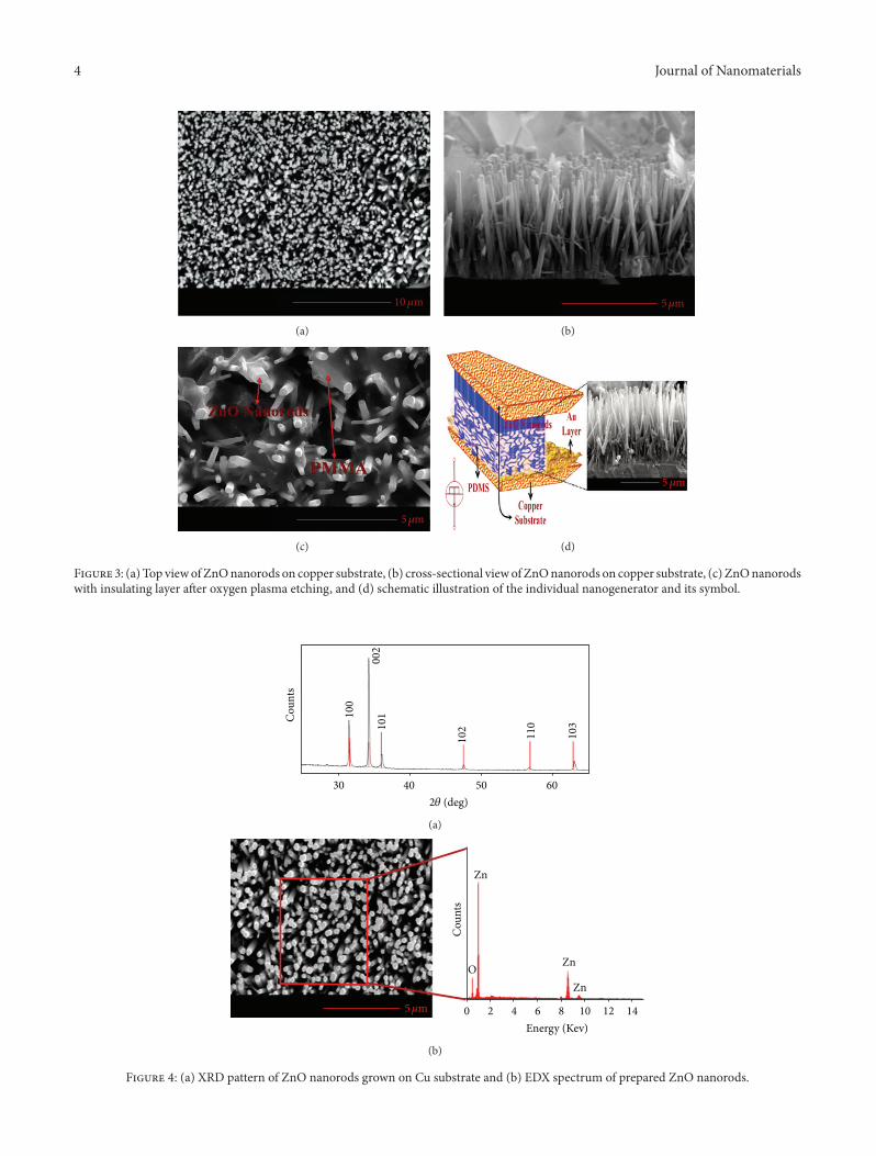
Figure 3: (a) Top viewof ZnOnanorods on copper substrate, (b) cross-sectional viewof ZnOnanorods on copper substrate, (c) ZnOnanorodswith insulating layer after oxygen plasma etching, and (d) schematic illustration of the individual nanogenerator and its symbol.
Cou
nts
30
100
101
002
102 110
103
40 50 602𝜃 (deg)
(a)
Cou
nts
0 2 4 6 8 10 12 14
Zn
Zn
Zn
O
Energy (Kev)
5 𝜇m
(b)
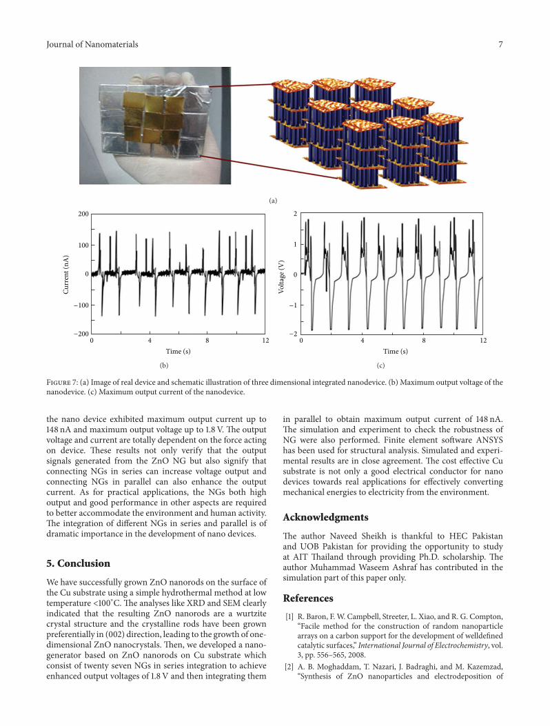
Figure 4: (a) XRD pattern of ZnO nanorods grown on Cu substrate and (b) EDX spectrum of prepared ZnO nanorods.

Journal of Nanomaterials 5
Figure 5: Schematic illustration of integrated NG.
from each other, at a speed of 2000 rpm for 30 seconds andthen annealed it at 100∘C for 1 minute. Reactive ion etchingwas used to etch PMMA layer to expose the tips of thenanorods. The results of fabrication will be given in the nextsection.
4. Results and Discussion
4.1. Characterization. The characterization was performedto determine morphology and size of the ZnO nanorodsby using SEM (Hitachi S3400, operated at 20 kV). Thecrystalline structure of aligned ZnO nanorods was observedusing XRD (Bruker, D8 Advance).The chemical compositionwas characterized by using energy dispersive spectroscopy(EDX).Then,NGwere assembled and tested.The, SEM imageof grown nanorods on Cu substrate is shown in Figure 3.
SEM image of spin coated PMMA layer is shown inFigure 3(c). The image undoubtedly indicates that spin coat-ing method of the insulating layer seals the gap between thenanorods and behaves like a protecting shield to insulatethem from each other. The surface of the nanorods wrappedwith PMMA is etched away after exposing to oxygen in thereactive ion etching.The zinc oxide nanorods were hexagonaland vertically aligned on the copper substrate. The diameterand length of the ZnO nanorods were 350–400 nm and 5-6 𝜇m, respectively. SEM images reveal that the nanorods arraywith the largest length and diameter was synthesized by thehydrothermal method.
The crystalline structure of aligned ZnO nanorods wasobserved using XRD with CuK𝛼 radiation, 𝜆 = 0.154 nmas shown in Figure 4(a) and EDX spectrum of the ZnOnanorods as shown in Figure 4(b). It is clear from Figure 4(b)that atomic ratio of Zn and oxygen (O) is ca. 1 : 1 that isindicating the perfect stoichiometric chemical compositionof the Zn and O in the nanorods.
XRD pattern of ZnO nanorods illustrates 6 reflectionpeaks of hexagonal wurtzite structure. These are (100),(002), (101), (102), (110), and (103) at 2𝜃 with correspondingangle 31.8∘, 34.4∘, 36.2∘, 47.6∘, 56.6∘, and 63.0∘, respectively.Compared with the other peaks, the (002) diffraction peakis much stronger in intensity. That confirms the nanorodswere aligned in the 𝑐-axis. Hence, they are acceptable inaccordance with (JCPDS) card no. 36-1451 with lattice con-stant 𝑎 = 3.24 A and 𝑐 = 5.21 A. The strong intensity
and narrow full width at half maximum (FWHM) of theXRD pattern shows that the ZnO nanorods synthesized hada good crystalline structure. To confirm the compositionof the grown nanorods, EDX analysis was performed. It isconfirmed from the EDX analysis that the grown nanorodsare indeed composed of Zn and O only. The molecular ratioof Zn :O of the grown nanorods is evaluated from EDX andquantitative analysis data is close to 1 : 1. No other peak for anyother element has been found in the spectrum except O andZn which again confirmed that the grown nanorods are pureZnO.
4.2. Scheme for the Integration of (NG) and Characterization.The nanogenerator based on Cu substrate can easily beintegrated in parallel and series for increasing output voltageand current owing to the uniform growth of ZnO nanorodson Cu substrate and the simultaneous use of Cu substrate aslower and upper electrodes as shown in Figure 5.
To characterize the electrical performance of thenanogenerator we integrated the NG in series and parallelcombination, consisting of nine parts on the large area of Cuelectrode. The first combination including NG1, NG2, andNG3 was incorporated in parallel with three parts formingone unit.The second combination including NG𝛼, NG𝛽, andNG𝛾, was incorporated in parallel with three parts attachedin series with two units. The third combination includingNGa, NGb, and NGc, was integrated in parallel with threeparts serially attached with three units. To characterizethe performance of the NG, the NG array was testedby a convenient trigger system which could periodicallycompress and release at frequency of 3-4Hz. In case ofserial combination, we calculated the output voltage with theincrease in the number of serially incorporated unit. As thenumber of incorporated units increases from one to three inthe order of NG1, NG𝛼, and NGa and their output voltageincreases from 0.03V, 0.09V, and 0.13 V, respectively. Theunits integrated in series are simultaneously affected by thesame external force and their corresponding piezoelectricpotential in external load is summed, the output voltageincreases with the number of units, the output voltage alsoincreases in the order of NG2, NG𝛽, and NGb with 0.04V,0.09V, and 0.18 V, respectively. The possibility of serialintegration based on copper Cu in order of NG3, NG𝛾, andNGc with output voltage increases as 0.03V, 0.07V, and0.17 V, respectively. The all above combination is shown inFigure 6.
After that, we measured the output current for the NGintegrated in parallel with three parts, the parallel integrationof three parts includingNG1, NG2, andNG3 led to the outputcurrent of 18 nA.The 2nd integration which was composed oftwo layers including NG𝛼, NG𝛽, and NG𝛾 led to the outputcurrent of 38 nA. The 3rd integration which was composedof three layers including NGa, NGb and NGc led to theoutput current of 97 nA. The NG based on Cu substratecan be simply integrated not only in series for high outputbut also in parallel for the high output current without anyspecific size limit. Since the humanwalking andmovement ofautomobiles are usually occurring at various low frequencies,

6 Journal of Nanomaterials
0.2
0.1
0
−0.1
−0.2
0 2 4Time (s)
Volta
ge (V
)0.2
0.1
0
−0.1
−0.2
0 2 4Time (s)
Volta
ge (V
)
0.2
0.1
0
−0.1
−0.2
0 2 4Time (s)
Volta
ge (V
)
NG1 −0.03V −0.09V −0.13VNGaNG𝛼
(a)
0.2
0.1
0
−0.1
−0.2
0 2 4Time (s)
Volta
ge (V
)
0.2
0.1
0
−0.1
−0.2
0 2 4Time (s)
Volta
ge (V
)0.2
0.1
0
−0.1
−0.2
0 2 4Time (s)
Volta
ge (V
)
NG2 −0.04V −0.09V −0.18VNGbNG𝛽
(b)
0.2
0.1
0
−0.1
−0.2
0 2 4Time (s)
Volta
ge (V
)
0.2
0.1
0
−0.1
−0.2
0 2 4Time (s)
Volta
ge (V
)
0.2
0.1
0
−0.1
−0.2
0 2 4Time (s)
Volta
ge (V
)
NG3 −0.03V −0.07V −0.17VNGcNG𝛾
(c)
20
10
0
−10
−20
Curr
ent (
nA)
0 2 4Time (s)
−18nANG1+ NG2 + NG3
(d)
80
40
0
−40
−80
Curr
ent (
nA)
0 2 4Time (s)
−97nANGa + NGb + NGc
(e)
40
20
0
−20
−40
Curr
ent (
nA)
0 2 4Time (s)
−38nANG𝛼 + NG𝛽 + NG𝛾
(f)
Figure 6: (a) Incorporated units in the order of NG1, NG𝛼, and NGa and their output voltages 0.03V, 0.09V, and 0.13 V; (b) incorporatedunits in the order of NG2, NG𝛽, and NGb and their output voltages 0.04V, 0.09V, and 0.18 V; (c) incorporated units in the order of NG3,NG𝛾, and NGc and their output voltages 0.03V, 0.07V, and 0.17V; (d) output current of 18 nA by parallel combination of NG1, NG2, andNG3; (e) output current of 97 nA by three layered including NGa, NGb, and NGc; (f) output current of 38 nA by two layered combinationincluding NG𝛼, NG𝛽, and NG𝛾.
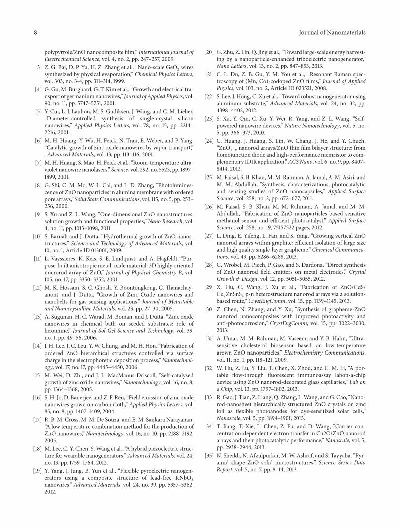
these stable results are promising for the use in practicalapplications. Photograph image of real device and schematicillustration of three-dimensional integrated nano device isshown in Figure 7.
Here, we design the device for energy scavenging fromhuman walking that is composed of three units. Thedevice was tightly fixed on smooth supporting to preventthe electrical noise. Under the human walking condition,
Journal of Nanomaterials 7
(a)
0 4 8 12Time (s)
Curr
ent (
nA)
200
100
0
−100
−200
(b)
0 4
2
1
0
8 12Time (s)
Volta
ge (V
)
−1
−2
(c)
Figure 7: (a) Image of real device and schematic illustration of three dimensional integrated nanodevice. (b) Maximum output voltage of thenanodevice. (c) Maximum output current of the nanodevice.
the nano device exhibited maximum output current up to148 nA and maximum output voltage up to 1.8 V. The outputvoltage and current are totally dependent on the force actingon device. These results not only verify that the outputsignals generated from the ZnO NG but also signify thatconnecting NGs in series can increase voltage output andconnecting NGs in parallel can also enhance the outputcurrent. As for practical applications, the NGs both highoutput and good performance in other aspects are requiredto better accommodate the environment and human activity.The integration of different NGs in series and parallel is ofdramatic importance in the development of nano devices.
5. Conclusion
We have successfully grown ZnO nanorods on the surface ofthe Cu substrate using a simple hydrothermal method at lowtemperature <100∘C. The analyses like XRD and SEM clearlyindicated that the resulting ZnO nanorods are a wurtzitecrystal structure and the crystalline rods have been grownpreferentially in (002) direction, leading to the growth of one-dimensional ZnO nanocrystals. Then, we developed a nano-generator based on ZnO nanorods on Cu substrate whichconsist of twenty seven NGs in series integration to achieveenhanced output voltages of 1.8 V and then integrating them
in parallel to obtain maximum output current of 148 nA.The simulation and experiment to check the robustness ofNG were also performed. Finite element software ANSYShas been used for structural analysis. Simulated and experi-mental results are in close agreement. The cost effective Cusubstrate is not only a good electrical conductor for nanodevices towards real applications for effectively convertingmechanical energies to electricity from the environment.
Acknowledgments
The author Naveed Sheikh is thankful to HEC Pakistanand UOB Pakistan for providing the opportunity to studyat AIT Thailand through providing Ph.D. scholarship. Theauthor Muhammad Waseem Ashraf has contributed in thesimulation part of this paper only.
References
[1] R. Baron, F. W. Campbell, Streeter, L. Xiao, and R. G. Compton,“Facile method for the construction of random nanoparticlearrays on a carbon support for the development of welldefinedcatalytic surfaces,” International Journal of Electrochemistry, vol.3, pp. 556–565, 2008.
[2] A. B. Moghaddam, T. Nazari, J. Badraghi, and M. Kazemzad,“Synthesis of ZnO nanoparticles and electrodeposition of
8 Journal of Nanomaterials
polypyrrole/ZnO nanocomposite film,” International Journal ofElectrochemical Science, vol. 4, no. 2, pp. 247–257, 2009.
[3] Z. G. Bai, D. P. Yu, H. Z. Zhang et al., “Nano-scale GeO2wires
synthesized by physical evaporation,” Chemical Physics Letters,vol. 303, no. 3-4, pp. 311–314, 1999.
[4] G. Gu,M. Burghard, G. T. Kim et al., “Growth and electrical tra-nsport of germaniumnanowires,” Journal of Applied Physics, vol.90, no. 11, pp. 5747–5751, 2001.
[5] Y. Cui, L. J. Lauhon, M. S. Gudiksen, J. Wang, and C. M. Lieber,“Diameter-controlled synthesis of single-crystal siliconnanowires,” Applied Physics Letters, vol. 78, no. 15, pp. 2214–2216, 2001.
[6] M. H. Huang, Y. Wu, H. Feick, N. Tran, E. Weber, and P. Yang,“Catalytic growth of zinc oxide nanowires by vapor transport,”, Advanced Materials, vol. 13, pp. 113–116, 2001.
[7] M. H. Huang, S. Mao, H. Feick et al., “Room-temperature ultra-violet nanowire nanolasers,” Science, vol. 292, no. 5523, pp. 1897–1899, 2001.
[8] G. Shi, C. M. Mo, W. L. Cai, and L. D. Zhang, “Photolumines-cence of ZnOnanoparticles in aluminamembranewith orderedpore arrays,” Solid State Communications, vol. 115, no. 5, pp. 253–256, 2000.
[9] S. Xu and Z. L. Wang, “One-dimensional ZnO nanostructures:solution growth and functional properties,”Nano Research, vol.4, no. 11, pp. 1013–1098, 2011.
[10] S. Baruah and J. Dutta, “Hydrothermal growth of ZnO nanos-tructures,” Science and Technology of Advanced Materials, vol.10, no. 1, Article ID 013001, 2009.
[11] L. Vayssieres, K. Keis, S. E. Lindquist, and A. Hagfeldt, “Pur-pose-built anisotropie metal oxide material: 3D highly orientedmicrorod array of ZnO,” Journal of Physical Chemistry B, vol.105, no. 17, pp. 3350–3352, 2001.
[12] M. K. Hossain, S. C. Ghosh, Y. Boontongkong, C. Thanachay-anont, and J. Dutta, “Growth of Zinc Oxide nanowires andnanobelts for gas sensing applications,” Journal of Metastableand Nanocrystalline Materials, vol. 23, pp. 27–30, 2005.
[13] A. Sugunan, H. C. Warad, M. Boman, and J. Dutta, “Zinc oxidenanowires in chemical bath on seeded substrates: role ofhexamine,” Journal of Sol-Gel Science and Technology, vol. 39,no. 1, pp. 49–56, 2006.
[14] J. H. Lee, I. C. Leu, Y.W. Chung, andM.H. Hon, “Fabrication ofordered ZnO hierarchical structures controlled via surfacecharge in the electrophoretic deposition process,” Nanotechnol-ogy, vol. 17, no. 17, pp. 4445–4450, 2006.
[15] M. Wei, D. Zhi, and J. L. MacManus-Driscoll, “Self-catalysedgrowth of zinc oxide nanowires,” Nanotechnology, vol. 16, no. 8,pp. 1364–1368, 2005.
[16] S. H. Jo, D. Banerjee, and Z. F. Ren, “Field emission of zinc oxidenanowires grown on carbon cloth,” Applied Physics Letters, vol.85, no. 8, pp. 1407–1409, 2004.
[17] R. B. M. Cross, M. M. De Souza, and E. M. Sankara Narayanan,“A low temperature combination method for the production ofZnO nanowires,” Nanotechnology, vol. 16, no. 10, pp. 2188–2192,2005.
[18] M. Lee, C. Y. Chen, S.Wang et al., “A hybrid piezoelectric struc-ture for wearable nanogenerators,” Advanced Materials, vol. 24,no. 13, pp. 1759–1764, 2012.
[19] Y. Yang, J. Jung, B. Yun et al., “Flexible pyroelectric nanogen-erators using a composite structure of lead-free KNbO
3
nanowires,” Advanced Materials, vol. 24, no. 39, pp. 5357–5362,2012.
[20] G. Zhu, Z. Lin,Q. Jing et al., “Toward large-scale energy harvest-ing by a nanoparticle-enhanced triboelectric nanogenerator,”Nano Letters, vol. 13, no. 2, pp. 847–853, 2013.
[21] C. L. Du, Z. B. Gu, Y. M. You et al., “Resonant Raman spec-troscopy of (Mn, Co)-codoped ZnO films,” Journal of AppliedPhysics, vol. 103, no. 2, Article ID 023521, 2008.
[22] S. Lee, J. Hong, C. Xu et al., “Toward robust nanogenerator usingaluminum substrate,” Advanced Materials, vol. 24, no. 32, pp.4398–4402, 2012.
[23] S. Xu, Y. Qin, C. Xu, Y. Wei, R. Yang, and Z. L. Wang, “Self-powered nanowire devices,” Nature Nanotechnology, vol. 5, no.5, pp. 366–373, 2010.
[24] C. Huang, J. Huang, S. Lin, W. Chang, J. He, and Y. Chueh,“ZnO
1−𝑥nanorod arrays/ZnO thin film bilayer structure: from
homojunction diode and high-performancememristor to com-plementary 1D1R application,”ACSNano, vol. 6, no. 9, pp. 8407–8414, 2012.
[25] M. Faisal, S. B. Khan, M.M. Rahman, A. Jamal, A. M. Asiri, andM. M. Abdullah, “Synthesis, characterizations, photocatalyticand sensing studies of ZnO nanocapsules,” Applied SurfaceScience, vol. 258, no. 2, pp. 672–677, 2011.
[26] M. Faisal, S. B. Khan, M. M. Rahman, A. Jamal, and M. M.Abdullah, “Fabrication of ZnO nanoparticles based sensitivemethanol sensor and efficient photocatalyst,” Applied SurfaceScience, vol. 258, no. 19, 75157522 pages, 2012.
[27] L. Ding, E. Yifeng, L. Fan, and S. Yang, “Growing vertical ZnOnanorod arrays within graphite: efficient isolation of large sizeand high quality single-layer grapheme,”Chemical Communica-tions, vol. 49, pp. 6286–6288, 2013.
[28] G. Wrobel, M. Piech, P. Gao, and S. Dardona, “Direct synthesisof ZnO nanorod field emitters on metal electrodes,” CrystalGrowth & Design, vol. 12, pp. 5051–5055, 2012.
[29] X. Liu, C. Wang, J. Xu et al., “Fabrication of ZnO/CdS/Cu2ZnSnS
4p-n heterostructure nanorod arrays via a solution-
based route,” CrystEngComm, vol. 15, pp. 1139–1145, 2013.[30] Z. Chen, N. Zhang, and Y. Xu, “Synthesis of grapheme-ZnO
nanorod nanocomposites with improved photoactivity andanti-photocorrosion,” CrystEngComm, vol. 15, pp. 3022–3030,2013.
[31] A. Umar, M. M. Rahman, M. Vaseem, and Y. B. Hahn, “Ultra-sensitive cholesterol biosensor based on low-temperaturegrown ZnO nanoparticles,” Electrochemistry Communications,vol. 11, no. 1, pp. 118–121, 2009.
[32] W. Hu, Z. Lu, Y. Liu, T. Chen, X. Zhou, and C. M. Li, “A por-table flow-through fluorescent immunoassay labon-a-chipdevice using ZnO nanorod-decorated glass capillaries,” Lab ona Chip, vol. 13, pp. 1797–1802, 2013.
[33] R.Gao, J. Tian, Z. Liang,Q. Zhang, L.Wang, andG.Cao, “Nano-rod-nanosheet hierarchically structured ZnO crystals on zincfoil as flexible photoanodes for dye-sensitized solar cells,”Nanoscale, vol. 5, pp. 1894–1901, 2013.
[34] T. Jiang, T. Xie, L. Chen, Z. Fu, and D. Wang, “Carrier con-centration-dependent electron transfer in Cu2O/ZnO nanorodarrays and their photocatalytic performance,” Nanoscale, vol. 5,pp. 2938–2944, 2013.
[35] N. Sheikh, N. Afzulpurkar, M. W. Ashraf, and S. Tayyaba, “Pyr-amid shape ZnO solid microstructures,” Science Series DataReport, vol. 5, no. 7, pp. 8–14, 2013.
Copyright © 2022 FDOKUMEN