Selective Crystalline Seed Layer Assisted Growth of Vertically Aligned MgZnO Nanowires and Their...
7
pubs.acs.org/crystal Published on Web 09/02/2009 r 2009 American Chemical Society DOI: 10.1021/cg900018p 2009, Vol. 9 4308–4314 Selective Crystalline Seed Layer Assisted Growth of Vertically Aligned MgZnO Nanowires and Their High-Brightness Field-Emission Behavior Dong Chan Kim, Bo Hyun Kong, Sanjay Kumar Mohanta, Hyung Koun Cho,* Jae Hong Park, and Ji Beom Yoo School of Advanced Materials Science and Engineering, Sungkyunkwan University, 300 Cheoncheon-dong, Jangan-gu, Suwon, Gyeonggi-do, 440-746, Korea Received January 8, 2009; Revised Manuscript Received July 9, 2009 ABSTRACT: This article reports a new approach for fabricating vertically aligned MgZnO nanowire arrays using selective crystalline seed layers deposited at relatively high temperatures by metalorganic chemical vapor deposition. In the phase- separated MgZnO seed layers, Zn-rich regions with a wurtzite structure allowed the growth of slim MgZnO nanowires, while the Mg-rich seeds with a cubic or amorphous-like structure hindered the formation of nanowires. The photoluminescence of these nanowires showed a remarkable increase in the activation energy of the excitons, ∼100 meV. The field-emission performance showed excellent emission behavior with extremely improved brightness, ∼80 times higher current density than that of the ZnO nanowires grown under the same conditions. Models for the growth evolution of slim nanowires on Si substrates were also proposed, based on microstructural characterization. 1. Introduction The synthesis of low-dimensional nanostructures in various forms has attracted considerable technological and scientific interest due to the physical and optical properties and the discovery of new physical meaning induced by the quantum- confinement effect. 1,2 One-dimensional (1D) ZnO nanostruc- tures (i.e., nanowires, nanorods, nanobelts, nanorings, etc.) have been the subject of intense research for applications in short-wavelength light-emitting devices and ultraviolet field emitters on account of their wide bandgap and high exciton binding energy, which can allow the production of devices with their performance unaffected by temperature. 3,4 Verti- cally aligned ZnO nanowire arrays are more suitable struc- tures for the fabrication of electronic devices, considering the interconnection of a metal layer and the feasibility of integra- tion processes. 5,6 The ZnO nanowires-based field emitters are expected to have a longer lifetime than carbon-based field emitters due to the chemical and environmental stability of oxide materials. Although many techniques have been used to synthesize vertically well-aligned ZnO nanowire arrays, 5-9 metalorganic chemical vapor deposition (MOCVD) has been demonstrated to be a promising tool with particular advan- tages of accurate doping, low-temperature, catalyst-free epi- taxial growth, etc. 9-11 However, this method produces dense and broad ZnO nanowires (>50 nm). Moreover, although the nanowires are highly crystalline with excellent optical quality, it is difficult to control the density and tip shape of the nanowires, which has a detrimental effect on the perfor- mance of field emitters due to the blunt tip shape and electric arcing. Therefore, the low emission intensity of ZnO-based field emitters and the difficulty in obtaining vertically aligned ZnO nanowire arrays with a narrower shape without the use of metal catalysts has limited field-emission applications to carbon nanotubes (CNTs). 12,13 In this context, the incorpora- tion of a small quantity of Mg atoms in the ZnO matrix can enhance the emission efficiency, 14,15 and an increase in synth- esis temperature can improve the crystalline quality and luminescence intensity. 16 Therefore, it is believed that both the addition of a small quantity Mg and the synthesis of vertically aligned nanowire arrays with the appropriate den- sity at high temperatures will lead to significant improvement in the field-emission behavior. This paper reports a method for synthesizing very slim, vertically aligned single crystalline MgZnO nanowire arrays by growing small wurtzite crystal- line Zn-rich phases selectively at high temperatures by MOCVD. The nanowires showed tremendous improvement in emission behavior due to the high crystalline quality and vertical alignment of nanowire arrays with the appropriate density at high growth temperatures. The detailed growth mechanism for these vertically aligned MgZnO nanowire arrays based on the microstructural characterizations is also presented. 2. Experimental Section 1D MgZnO nanowires were grown on Si substrates using a low- pressure MOCVD method, with diethylzinc (DEZn, purity 99.9995%), bis-cyclopentadienyl-magnesium (Cp 2 Mg, purity 99.9995%), and pure oxygen gas (O 2 , purity 99.9999%) as the reactive gases. Argon was used as the carrier gas. All Si substrates were degreased in an ultrasonic bath with acetone, ethanol, and deionized water for 5 min each. The Cp 2 Mg flow rate during the growth of MgZnO nanowires was 1.4 μmol/min, while the DEZn flow rates was kept constant at 6.1 μmol/min. The nanowires were grown at temperatures ranging from 450-500 °C with a reactor pressure of 1 Torr for 30 min. No buffer layers or metal catalysts were required to produce the vertically aligned nanowires in this MOCVD method. The maximum level of Mg incorporation in the ZnO that allows the synthesis of vertically aligned nanowires under these growth conditions was approximately ∼8 at %. The ZnO nanowires were also grown for comparison. The morphology of the fabricated nanowires was observed by field-emission scanning electron microscopy (FESEM, JSM6700F). The microstructure was examined by transmission electron micro- scopy (TEM, JEM 3010) and high-resolution TEM operated at 300 kV. The TEM specimens were prepared by mechanical polishing and ion- milling at a low current Ar þ ion dose to prevent deformation during *To whom correspondence should be addressed. E-mail: chohk@ skku.edu.
-
Upload
independent -
Category
Documents
-
view
0 -
download
0
Transcript of Selective Crystalline Seed Layer Assisted Growth of Vertically Aligned MgZnO Nanowires and Their...

pubs.acs.org/crystal Published on Web 09/02/2009 r 2009 American Chemical Society
DOI: 10.1021/cg900018p
2009, Vol. 94308–4314
Selective Crystalline Seed Layer Assisted Growth of Vertically Aligned
MgZnO Nanowires and Their High-Brightness Field-Emission Behavior
Dong Chan Kim, Bo Hyun Kong, Sanjay Kumar Mohanta, Hyung Koun Cho,*Jae Hong Park, and Ji Beom Yoo
School of Advanced Materials Science and Engineering, Sungkyunkwan University,300 Cheoncheon-dong, Jangan-gu, Suwon, Gyeonggi-do, 440-746, Korea
Received January 8, 2009; Revised Manuscript Received July 9, 2009
ABSTRACT: This article reports a new approach for fabricating vertically aligned MgZnO nanowire arrays using selectivecrystalline seed layers deposited at relatively high temperatures by metalorganic chemical vapor deposition. In the phase-separatedMgZnO seed layers, Zn-rich regionswith awurtzite structure allowed the growth of slimMgZnOnanowires, while theMg-rich seeds with a cubic or amorphous-like structure hindered the formation of nanowires. The photoluminescence of thesenanowires showed a remarkable increase in the activation energy of the excitons, ∼100 meV. The field-emission performanceshowed excellent emission behavior with extremely improved brightness,∼80 times higher current density than that of the ZnOnanowires grown under the same conditions. Models for the growth evolution of slim nanowires on Si substrates were alsoproposed, based on microstructural characterization.
1. Introduction
The synthesis of low-dimensional nanostructures in variousforms has attracted considerable technological and scientificinterest due to the physical and optical properties and thediscovery of new physical meaning induced by the quantum-confinement effect.1,2 One-dimensional (1D) ZnO nanostruc-tures (i.e., nanowires, nanorods, nanobelts, nanorings, etc.)have been the subject of intense research for applications inshort-wavelength light-emitting devices and ultraviolet fieldemitters on account of their wide bandgap and high excitonbinding energy, which can allow the production of deviceswith their performance unaffected by temperature.3,4 Verti-cally aligned ZnO nanowire arrays are more suitable struc-tures for the fabrication of electronic devices, considering theinterconnection of a metal layer and the feasibility of integra-tion processes.5,6 The ZnO nanowires-based field emitters areexpected to have a longer lifetime than carbon-based fieldemitters due to the chemical and environmental stability ofoxidematerials. Althoughmany techniques have been used tosynthesize vertically well-aligned ZnO nanowire arrays,5-9
metalorganic chemical vapor deposition (MOCVD) has beendemonstrated to be a promising tool with particular advan-tages of accurate doping, low-temperature, catalyst-free epi-taxial growth, etc.9-11 However, this method produces denseand broad ZnO nanowires (>50 nm). Moreover, althoughthe nanowires are highly crystalline with excellent opticalquality, it is difficult to control the density and tip shape ofthe nanowires, which has a detrimental effect on the perfor-mance of field emitters due to the blunt tip shape and electricarcing. Therefore, the low emission intensity of ZnO-basedfield emitters and the difficulty in obtaining vertically alignedZnO nanowire arrays with a narrower shape without the useof metal catalysts has limited field-emission applications tocarbon nanotubes (CNTs).12,13 In this context, the incorpora-tion of a small quantity of Mg atoms in the ZnO matrix can
enhance the emission efficiency,14,15 and an increase in synth-esis temperature can improve the crystalline quality andluminescence intensity.16 Therefore, it is believed that boththe addition of a small quantity Mg and the synthesis ofvertically aligned nanowire arrays with the appropriate den-sity at high temperatures will lead to significant improvementin the field-emission behavior. This paper reports a methodfor synthesizing very slim, vertically aligned single crystallineMgZnO nanowire arrays by growing small wurtzite crystal-line Zn-rich phases selectively at high temperatures byMOCVD. The nanowires showed tremendous improvementin emission behavior due to the high crystalline quality andvertical alignment of nanowire arrays with the appropriatedensity at high growth temperatures. The detailed growthmechanism for these vertically aligned MgZnO nanowirearrays based on the microstructural characterizations is alsopresented.
2. Experimental Section
1D MgZnO nanowires were grown on Si substrates using a low-pressureMOCVDmethod,withdiethylzinc (DEZn, purity 99.9995%),bis-cyclopentadienyl-magnesium (Cp2Mg, purity 99.9995%), and pureoxygengas (O2, purity 99.9999%) as the reactive gases.Argonwasusedas the carrier gas. All Si substrates were degreased in an ultrasonic bathwith acetone, ethanol, and deionized water for 5min each. The Cp2Mgflow rate during the growth of MgZnO nanowires was 1.4 μmol/min,while the DEZn flow rates was kept constant at 6.1 μmol/min. Thenanowires were grown at temperatures ranging from 450-500 �Cwitha reactor pressure of 1 Torr for 30 min. No buffer layers or metalcatalysts were required to produce the vertically aligned nanowires inthisMOCVDmethod. Themaximum level ofMg incorporation in theZnO that allows the synthesis of vertically aligned nanowires underthese growth conditions was approximately ∼8 at %. The ZnOnanowires were also grown for comparison.
The morphology of the fabricated nanowires was observed byfield-emission scanning electron microscopy (FESEM, JSM6700F).The microstructure was examined by transmission electron micro-scopy (TEM,JEM3010) andhigh-resolutionTEMoperated at 300kV.The TEM specimens were prepared bymechanical polishing and ion-milling at a low current Arþ ion dose to prevent deformation during
*To whom correspondence should be addressed. E-mail: [email protected].
Article Crystal Growth & Design, Vol. 9, No. 10, 2009 4309
ion-milling. Energy dispersive X-ray fluorescence (EDX) analysiswas carried out during the TEM observations with a nanobeam toprobe the distribution of Mg atoms in the MgZnO nanowires.Variable temperature photoluminescence (PL) measurements wereperformed by placing the samples inside a closed cycle He cryostatand using 325 nm He-Cd laser as the excitation source. The roomtemperature field-emission (FE) measurements were performed in ahighvacuumchamber at abasepressure of 8�10-7Torr.Thedistancebetween the electrodes was approximately 200 μm, while the samplesize was 15�15 mm2.
3. Results and Discussion
Figure 1 showsFESEMimages of the 1DZnOandMgZnOnanostructures synthesized on Si substrates at different tem-peratures (450-500 �C). The ZnO nanowires become moreslender and randomly inclined on the Si surface with increas-ing growth temperature (Figure 1a,b). At the highest growthtemperature of 500 �C,most of the nanowires containedmanybranches from the less dense seeds, and appeared to bemultipod nanostructures. Several studies have reported thatZnO nanowires form in the presence of a two-dimensional(2D) interfacial layer between the nanowires and substrate.9,17
In the present case, the vertically aligned ZnO nanowiresgrown at 450 �C had an interfacial layer, while the inclinednanowires observed at 500 �Cshowedno signof the formationof an interfacial layer. In the case of Mg incorporatednanowires, thewidth of theMgZnOnanowireswere narrowerthan that of ZnO. FESEM showed that the MgZnO nano-wires grown at high temperatures were vertically well-alignedwith a small inclination (Figure 1d). The length and diameterof the MgZnO nanowires grown at 500 �C were 2.8-3.0 μmand ∼10 nm, respectively. Figure 1e,f shows the θ-2θ XRDpatterns of the 1D ZnO and MgZnO nanostructures growndirectly on the Si substrates at 450-500 �C. These ZnO andMgZnO nanowires showed a highly preferred orientationalong the c-axis. However, the ZnO nanowires grown at500 �C showed a lower IZnO(0002)/ISi(100) intensity ratio, whichwas attributed to the random inclination and reduced densityof nanowires. On the other hand, the MgZnO nanowiresgrown on at the same temperature showed a considerablyenhanced IMgZnO(0002)/ISi(100) intensity ratio, highlighting thevertical alignment and high crystalline quality. The dominantdiffraction peaks at 34.5� correspond to the (0002) plane of a
Figure 1. Cross-sectional FESEM images of ZnO [(a) and (b)] and MgZnO [(c) and (d)] nanowires grown at 450 and 500 �C. The insets in(b) and (d) show the plane-view FESEM image of ZnO multipod nanostructures and magnified FESEM image of MgZnO nanowire arrays,respectively. Panels (e) and (f) θ-2θXRD curves of ZnO andMgZnO nanowires grown on Si substrates at 450 and 500 �C, respectively, wherethe y-axis scale is the same.
4310 Crystal Growth & Design, Vol. 9, No. 10, 2009 Kim et al.
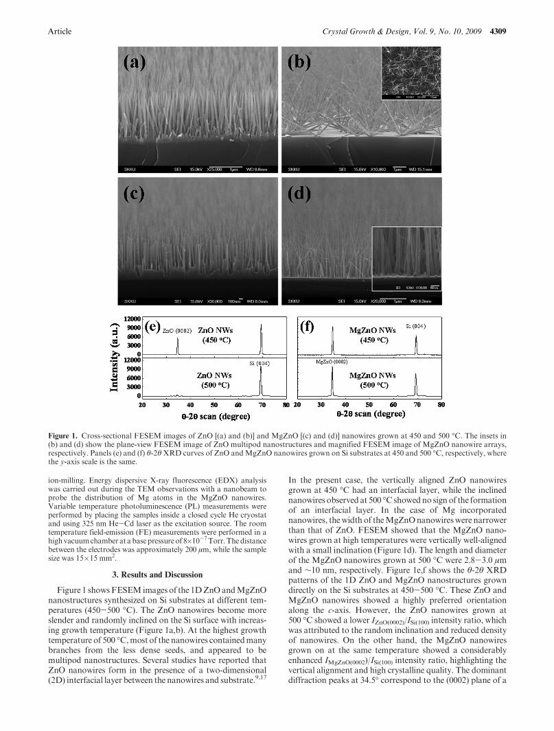
Figure 2. Cross-sectional TEM images of ZnO nanowires grown at 500 �C: (a) low magnification image showing multipod nanostructures,(b) the seed layer of a multipod nanostructure showing polycrystalline nature, (c) HRTEM image from the region without an interfacial layer,and (d) HRTEM image from the seed layer of a multipod nanostructure. The insets show the DPs revealing the crystal structure.
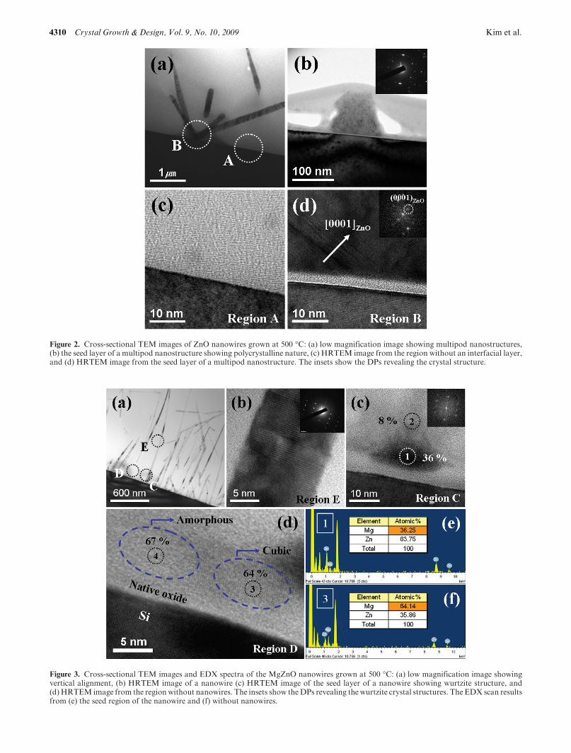
Figure 3. Cross-sectional TEM images and EDX spectra of the MgZnO nanowires grown at 500 �C: (a) low magnification image showingvertical alignment, (b) HRTEM image of a nanowire (c) HRTEM image of the seed layer of a nanowire showing wurtzite structure, and(d)HRTEM image from the regionwithout nanowires. The insets show theDPs revealing the wurtzite crystal structures. The EDX scan resultsfrom (e) the seed region of the nanowire and (f) without nanowires.
Article Crystal Growth & Design, Vol. 9, No. 10, 2009 4311
wurtzite ZnO and MgZnO crystal. To the best of our knowl-edge, this width is the narrowest among the vertically alignednanowires fabricated by MOCVD. The formation of verti-cally aligned nanostructures with a narrow tip shape, whichcan be obtained at high processing temperatures, is suitablefor applications as high efficiency field emitters in field-emission displays (FEDs).18,19 However, the results show thateven though an increase in growth temperature allows theproduction of single crystal ZnO nanowires with high crystal-line quality, inclination of the nanowires occurred at highergrowth temperature (Figure 1b). Therefore, there is a limit forthe realization of vertically aligned and slim ZnO nanowiresby increasing the growth temperature. Interestingly, the in-corporation of Mg atoms in the ZnO nanowires leads to theformation of vertically aligned nanowires at a relatively highgrowth temperature, as shown in Figure 1d.
TEM and HRTEM were used to characterize the micro-structural behavior on the incorporation of Mg in the nano-wires grown at 500 �C. Figures 2 and 3 show TEM images ofthe inclined ZnO nanowires and vertically aligned MgZnOnanowires, respectively, grown at the same temperature.Dense ZnO multipod structures with many nanowires origi-nating from the same seed were formed at higher synthesistemperatures (Figure 2a). The seed of the multipod containedlarge grains, approximately 142 nm in width (Figure 2b). No
2D thin filmswere actually deposited on the substrate surface,as shown in Figure 2c. The magnified HRTEM image of theseeds shows a polycrystalline behavior with a random align-ment of (0002)ZnO planes (Figure 2d). On the other hand,MgZnO nanowires grown at 500 �C showed good verticalalignment, despite being very slim and grown at high tem-peratures (Figure 3a). The HRTEM image and diffractionpatterns (DPs) of a vertically aligned MgZnO nanowirerevealed the nanowires to be single crystal wurtzite structureswith a c-axis preferred orientation, that is, along the [0002]direction (Figure 3b). The seeds of the MgZnO nanowireswere 20 nm in diameter and exhibited a single crystal wurtzitestructure with a c-axis preferred orientation, as shown inFigure 3c. Therefore, the seeds in both ZnO and MgZnOnanowires act as templates on the growth of the respectivenanowires. Because all ZnObased nanowireswere grownwitha c-axis preferred orientation, the ZnO on the polycrystallineseeds led to the formation of ZnO multipod structures, whiletheMgZnOon single crystal seeds resulted in the formation ofvertically aligned MgZnO nanowires. On the other hand, theSi substrate surface, where nanowires were not formed,showed a slightly different contrast, as shown in Figure 3d.This region consists of a native silicon dioxide layer and a thinlayer with a 5 nm thickness. A part of the thin layer showedlattice fringes or atomic images indicating a crystal, and the
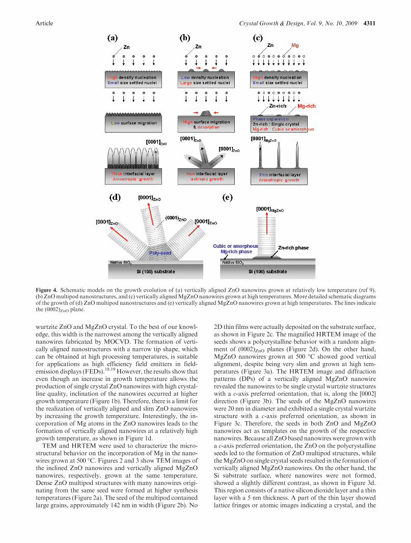
Figure 4. Schematic models on the growth evolution of (a) vertically aligned ZnO nanowires grown at relatively low temperature (ref 9),(b) ZnOmultipod nanostructures, and (c) vertically alignedMgZnOnanowires grown at high temperatures.More detailed schematic diagramsof the growth of (d) ZnOmultipod nanostructures and (e) vertically alignedMgZnO nanowires grown at high temperatures. The lines indicatethe (0002)ZnO plane.
4312 Crystal Growth & Design, Vol. 9, No. 10, 2009 Kim et al.
other showed an amorphous-like image. Interestingly, thesecrystals had a cubic structure not a wurtzite structure. There-fore, the formation of vertically well aligned nanowires with asingle crystal wurtzite structure was attributed to the smallislands with a wurtzite structure embedded in the cubic oramorphous structure matrix during the initial stages ofgrowth. Furthermore, Figure 3e,f shows EDX point scansof the distribution of Mg atoms on different regions of theMgZnO nanowires. The Mg content in the seed layer with awurtzite structure was relatively high, 36 at % (Figure 3c,e),while the averageMg composition in the body of theMgZnOnanowire was approximately∼8 at%, where theMg compo-sition in the body of the MgZnO nanowire is uniform alongthe nanowires with the deviation of below 1% except the seedregion. According to previous reports, theMg composition of∼36 at%might be themaximumvalue showingMgZnOwitha stablewurtzite structure, while the theoretical solubility limitis only 4 at %.20,21 Furthermore, the thin layers formed in theregion containing no nanowires on the Si surface have aremarkably high Mg composition (g60 at %) with a cubicphase structure (Figure 3d,f). Earlier, it was also reported thattheMgZnO layers containingmore than 60 at%Mg formed acubic phase, which is consistent with our observations.22,23
The Mg-rich cubic or amorphous-like regions at the initialstage did not form nanowires in continuous growth due to thesuppression of the wurtzite structure nanowires.
Considering the microstructural behaviors and Mg distri-bution in the nanowires, schematic growth models wereproposed to explain the growth evolution of the verticallyalignedMgZnO nanowires and the ZnOmultipod nanostruc-tures on the Si substrates at high processing temperatures, asdemonstrated in Figure 4. A recent study proposed a growthmodel for vertically aligned ZnO nanorods in the presence ofthe interfacial layer, in which the defects observed in theinterfacial layer play a key role in nanorod growth(Figure 4a).9 In general, three-dimensional island growth isdesirable in heterostructures with large lattice mismatch, such
as ZnO/Si substrates, which leads to a decrease in contactarea. In addition, based on the conventional nucleation andgrowth model, an increase in growth temperature promotessurface migration of the as-deposited atoms resulting in theagglomeration of the nucleated islands, as shown inFigure 4b.24 The agglomerated islands contain several grainswith different orientations from each other, and the deposi-tion of ZnO nanowires proceeds along the c-axis crystalorientation of the seed layer to form ZnO multipod nanos-tructures (Figure 4d). In contrast, MgZnO nanowires withvertical alignment and a high aspect ratio were synthesizedwith the assistance of small size wurtzite islands (Figure 4c).At the initial stage, Mg incorporation in ZnO is expected todisturb the surfacemigration of the as-deposited atoms due tothe relatively high adsorption energy ofMg metal adatoms.25
Several groups reported that theMgZnOalloywith a highMgcomposition showed phase separation into wurtzite Zn-richand rocksalt Mg-rich phases under thermal equilibrium con-ditions due to the thermodynamic solubility limit of Mg inZnO.22,23 These reports are consistent with the present resultsshowing the formation of thin MgZnO layers with a cubic oramorphous-like Mg-rich phase and a wurtzite Zn-rich phaseat the initial stages of growth, as shown in Figures 3 and 4c.After forming the seed layers, wurtzite phase MgZnO nano-wires with ∼ 8% Mg formed selectively on the wurtzite seedand grew vertically on the Si substrates, as shown inFigure 4e.
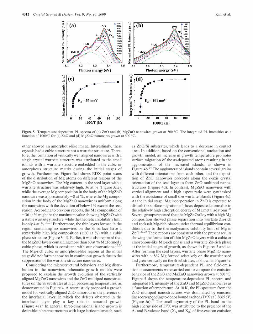
Furthermore, temperature-dependent PL and field-emis-sion measurements were carried out to compare the emissionbehavior of the ZnO andMgZnOnanowires grown at 500 �C.Figure 5 shows the temperature-dependent PL spectra andintegrated PL intensity of the ZnO andMgZnO nanowires asa function of temperature. At 10K, the PL spectrum from theZnO multipod nanostructures was dominated by emissionlines corresponding todonorboundexciton (D0Xat 3.3665 eV)(Figure 5a).26 The small asymmetry of the PL band on thehigh energy side of D0X was attributed to the presence of theA- and B-valence band (XA and XB) of free-exciton emission
Figure 5. Temperature-dependent PL spectra of (a) ZnO and (b) MgZnO nanowires grown at 500 �C. The integrated PL intensities as afunction of 1000/T for (c) ZnO and (d) MgZnO nanowires grown at 500 �C.
Article Crystal Growth & Design, Vol. 9, No. 10, 2009 4313
and their excited states transitions.27,28 The PL spectrum alsoshows a broad low energy shoulder at around 3.314 eV(leveled as “P”) along with its LO phonon replicas at 3.238and 3.167 eV with an energy separation of 76 and 147 meV,respectively. The P line can be resolved into two-electronsatellites, a donor-to-acceptor pair, exciton-exciton scatter-ing, andLO-phonon replicas of FXandD0X.With increasingtemperature, the intensity of D0X decreases whereas that ofFX increases and becomes dominant above 100 K due to thethermal dissociation of the bound exciton to free exciton athigher temperature. The PL spectrum at room temperatureshows the exciton emission from the ZnO nanowires with apeakposition at 3.27 eV. In contrast toZnO, the PL spectra oftheMgZnOnanowires showablue shift in thenear-band-edgeexcitonic emissions, as shown in Figure 5b. The 10 K PLspectrum from the MgZnO nanorods is dominated by emis-sion lines corresponding to donor bound exciton (D0X at3.393 eV) and P line (at 3.323 eV), and its phonon replicas at3.246 and 3.171 eV. The PL spectrum from the MgZnOnanowires at room temperature shows exciton emission witha peak at 3.345 eV. Hence, there was a blue shift of 75 meV inthe room-temperature PL spectrum of MgZnO nanowireswhen compared to ZnO nanowires. It was reported that theexciton transition energy (Eex) of MgZnO varies with Mgcontent in accordance with E(MgxZn1-xO)=E(ZnO) þ 1.64x [eV].29 From this equation, the estimatedMg content in theMgZnOnanowires with an emission energy of 3.53 eVwas∼5at %, which is close to the value estimated by EDX. The PLpeak shift can also be associated with laser heating or stress/strain in the film.30,31 No shift in the PL peak position due tolaser heating was expected because the laser power was keptvery low (<3 mW) during the PL measurement. As differentacquisition timesmay cause apeak shift under prolonged laserirradiation, the acquisition time of all spectra were also keptconstant. Furthermore, the length of the MgZnO nanowireswere 2.8-3.0 μm, and the penetration depth of the laser lightat 325 nm was 60-120 nm. Therefore, the observed PLemission originates from the top region of the MgZnOnanowires only, and the top of the nanorods is expected tobe stress free. Therefore, the observed blue-shift from theMgZnO nanowires is not believed to be related to the stresseffect, but toMg incorporation in ZnO. Figure 5b showed thedecrease in the contribution of the LO phonon to the emis-sions spectra of MgZnO nanowires compared to ZnO multi-pod nanostructures, indicating a reduction in the couplingstrength of the exciton-phonon interaction with Mg incor-poration. Polar semiconductors experience a strong Frohlich
electron-phonon interaction that gives rise to an exciton-LOphonon interaction. Recently, Pan et al.28 have reporteda decrease in exciton-LO phonon coupling strength withincreasingMgcontent inMgZnOnanocrystals. Earlier,Wanget al.32 extracted the exciton-LO phonon coupling parameterof ZnO nanowires by resonant Raman scattering, and foundthat coupling strength decreases with decreasing nanowirediameter. Thus, the reduction of the exciton-LO phononcoupling strength of MgZnO nanowires compared to ZnOmultipod nanostructures is due to the combined effect of Mgincorporation in ZnO and the decrease in nanowire diameter.The thermal activation energy (Ea) of ZnO and MgZnOnanowires were calculated from the Arrhenius plot of thePL results showing the behavior of the integrated intensity as afunction of temperature (Figure 5c,d). The activation energyrelated to the high temperature regime for ZnO and MgZnOnanowires were approximately 57 and 101 meV, respectively.This activation energy for ZnO nanowires is similar to thebinding energy of the free exciton (59 meV). In contrast, theactivation energy for the MgZnO nanowires increased withthe slow quenching of the integrated intensity with increasingtemperature when compared to ZnO. This suggests that thefree excitons can survive at relatively high temperatures, and itis expected to have stable device operation at high tempera-tures. The increase in activation energy inMgZnO nanowireswas attributed to the larger impuritybinding energyor carrier/exciton localization energy withMg incorporation. Recently,Wassner et al. observed a relatively higher activation energyof127 meV for MgZnO thin films with Mg contents x=0.37.33
In addition, the MgZnO films showed a relatively higheractivation energy due to the carrier localization effect fromphase separation.14 However, in this case, the observed PLemission originatedmainly from the top region of theMgZnOnanowires. Therefore, an increase in activation energy due tothe quantum confinement effect cannot be excluded in suchslim nanowires with a diameter < 20 nm.
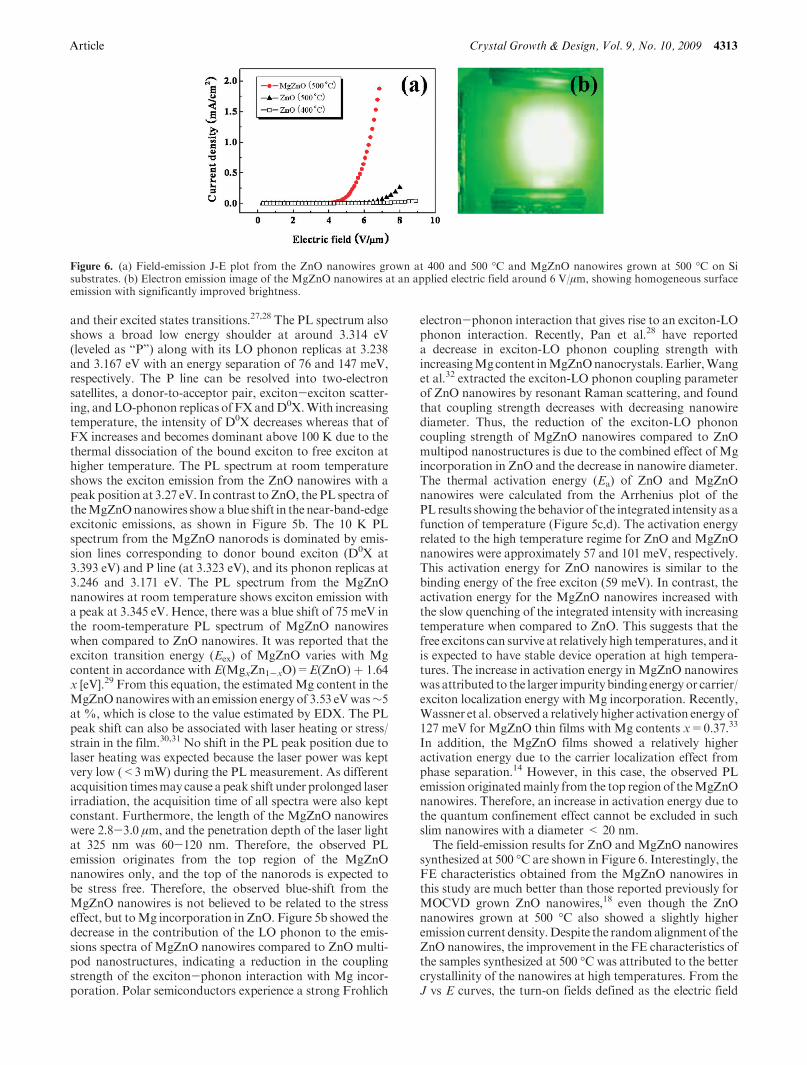
The field-emission results for ZnO and MgZnO nanowiressynthesized at 500 �C are shown in Figure 6. Interestingly, theFE characteristics obtained from the MgZnO nanowires inthis study are much better than those reported previously forMOCVD grown ZnO nanowires,18 even though the ZnOnanowires grown at 500 �C also showed a slightly higheremission current density.Despite the randomalignment of theZnO nanowires, the improvement in the FE characteristics ofthe samples synthesized at 500 �C was attributed to the bettercrystallinity of the nanowires at high temperatures. From theJ vs E curves, the turn-on fields defined as the electric field
Figure 6. (a) Field-emission J-E plot from the ZnO nanowires grown at 400 and 500 �C and MgZnO nanowires grown at 500 �C on Sisubstrates. (b) Electron emission image of the MgZnO nanowires at an applied electric field around 6 V/μm, showing homogeneous surfaceemission with significantly improved brightness.
4314 Crystal Growth & Design, Vol. 9, No. 10, 2009 Kim et al.
corresponding to a current density of 0.1 μA/cm2were 3.8 and2.7 V/μm for the ZnO and MgZnO nanowires synthesized at500 �C, respectively (Figure 6a). However, the most remark-abledifference in theFEresults is the current density.At6V/μm,the MgZnO nanowires with vertical alignment and a nar-rowwidth showed a current density approximately 80 timeshigher than that of the ZnO nanowires. The electric fieldrequired for a current density of 1mA/cm2 is approximately6 V/μm, which corresponds to the minimum emissioncurrent density for the operation of a video graphics arrayFED. Moreover, the Si integration process can be utilizedwith these vertically aligned MgZnO nanowire arrays onlarge size Si substrates. This tremendous increase in the FEcharacteristics was attributed to the simultaneous achieve-ment of the improved crystalline quality at high-tempera-tures, and vertical alignment of the nanowire arrays withthe appropriate density. Figure 6b shows an electron emis-sion image of the transparent anode at an applied electricfield of approximately 6 V/μmduring the FEmeasurement.This suggests that the entire surface emission is remarkablybright and homogeneous.
4. Conclusions
In summary, we have successfully realized the high-brightness field-emission performance from the verticallyaligned and slim MgZnO nanowire arrays synthesized byMOCVD at a relatively high temperature of 500 �C. Theevolution of the vertically aligned MgZnO nanowires athigher growth temperatures was attributed to the forma-tion of small size selective crystalline seeds with a wurtzitestructure, which acted as a template for nanowire growth.In contrast, ZnO nanowires grown at high temperaturesshowed multipod nanostructures with nanowires originat-ing from large size polycrystalline grains. The temperature-dependent PL results from the vertically aligned MgZnOnanowires revealed the slow quenching of exciton-relatedemission with a thermal activation energy of ∼101 meV,which allows stable device operation at high temperatures.The remarkable increase in the emission intensity of theMgZnO nanowires (∼80 times higher than ZnO nanowires)was attributed to the achievement of high crystalline qualityand vertically aligned slim nanowires with the appropriatedensity. On the basis of microstructural characterization,growth models were proposed to explain the growth evolu-tion of slim nanowires on a Si substrate.
Acknowledgment. This work was supported by the KRFGrant (KRF-2007-521-D00191) and Grant No. the KoreaScience and Engineering Foundation (KOSEF) grant fundedby the Korea government (MEST) (No. 2009-0078876). Thisresearch was also financially supported by the Ministry ofKnowledge Economy (MKE) and Korea Industrial Technol-ogy Foundation (KOTEF) through the Human ResourceTraining Project for Strategic Technology.
References
(1) Pavesi, L.; Negro, D. L.; Mazzoleni, C.; Franzo, G.; Priolo, F.Nature 2000, 408, 440.
(2) Jiang, X.; Xiong, Q.; Nam, S.; Qian, F.; Li, Y.; Lieber, C.M.NanoLett. 2007, 7, 3214.
(3) Kong, X. Y.; Wang, Z. L. Nano Lett. 2003, 3, 1625.(4) Wu, J. J.; Liu, S. C. Adv. Mater. 2002, 14, 215.(5) Park, W. I.; Yi, G. -C. Adv. Mater. 2004, 16, 87.(6) Sun,X.W.;Huang, J.Z.;Wang, J.X.;Xu,Z.NanoLett.2008,8, 1219.(7) Nobis, T.; Kaidashev, E. M.; Rahm, A.; Lorenz, M.; Lenzner, J.;
Grundmann, M. Nano Lett. 2004, 4, 797.(8) Huang, M. H.; Mao, S.; Feick, H.; Yan, H.; Wu, Y.; Kind, H.;
Weber, E.; Russo, R.; Yang, P. Science 2001, 292, 1897.(9) Park, D. J.; Lee, J. Y.; Kim, D. C.; Mohanta, S. K.; Cho, H. K.
Appl. Phys. Lett. 2007, 91, 143115.(10) Gruber, Th.; Kirchner, C.; Kling, R.; Reuss, F.; Waag, A. Appl.
Phys. Lett. 2004, 84, 5359.(11) Zhang, B. P.; Bihn, N. T.; Wakatsuki, K.; Liu, C. Y.; Segawa, Y.;
Usami, N. Appl. Phys. Lett. 2005, 86, 032105.(12) Wang, M. S.; Peng, L. M.; Wang, J. Y.; Chen, Q. J. Phys. Chem. B
2005, 109, 110.(13) Jung, S.M.;Hahn, J.; Jung,H.Y.; Suh, J. S.NanoLett. 2006, 6, 1569.(14) Shibata, H.; Tampo, H.;Matsubara, K.; Yamada, A.; Sakurai, K.;
Ishizuka, S.; Niki, S.; Sakai, M.Appl. Phys. Lett. 2007, 90, 124104.(15) Hill,M.R.;Russell, J. J.; Lamb,R.N.Chem.Mater. 2008, 20, 2461.(16) Shan, F. K.; Liu, G. X.; Lee, W. J.; Shin, B. C. J. Appl. Phys. 2007,
101, 053106.(17) Cong, G.W.;Wei, H. Y.; Zhang, P. F.; Peng,W. Q.;Wu, J. J.; Liu,
X. L.; Jiao, C. M.; Hu, W. G.; Zhu, Q. S.; Wang, Z. G.Appl. Phys.Lett. 2005, 87, 231903.
(18) Kim, D. C.; Kong, B. H.; Jeon, S. Y.; Yoo, J. B.; Cho, H. K.; Park,D. J.; Lee, J. Y. J. Mater. Res. 2007, 22, 2032.
(19) Yang,C. -J.;Wang,S. -M.;Liang, S.-W.;Liang, S. -W.;Chang,Y. -H.;Chen, C.; Shieh, J. -M. Appl. Phys. Lett. 2007, 90, 033104.
(20) Vashei, Z.; Minegishi, T.; Suzuki, H.; Hanada, T.; Cho, M. W.;Yao, T.; Setiawan, A. J. Appl. Phys. 2005, 98, 054911.
(21) Bhattacharya, P.; Das, R. R.; Katiyar, R. S.Appl. Phys. Lett. 2003,83, 2010.
(22) Yang,W.;Hullavarad, S. S.;Nagaraj, B.; Takeuchi, I.; Sharma,R. P.;Venkatesan, T.; Vispute, R. D.; Shen, H. Appl. Phys. Lett. 2003, 82,3424.
(23) Chen, J.; Shen, W. Z. Appl. Phys. Lett. 2003, 83, 2154.(24) Wang,Y.G.;Lau,S.P;Lee,H.W.;Yu,S.F.;Tay,B.K.;Zhang,X.H.;
Hng, H. H. J. Appl. Phys. 2003, 94, 354.(25) Kim,M.; Hong, Y. J.; Yoo, J.; Yi, G.-C.; Park, G.-S.; Kong, K.-J.;
Chang, H. Phys. Stat. Sol. (RRL) 2008, 2, 197.(26) Meyer, B. K.; Alves; Hofmann, H. D. M.; Kriegseis, W.; Forster,
D.; Bertram, F.; Christen, J.; Hoffmann, A.; StraBburg, M.;Dworzak, M.; Haboeck, U.; Rodina, A. V. Phys. Stat. Sol.(b) 2004, 241, 231.
(27) Teke, A.; Ozgur, U.; Dogan, S.; Gu, X.; Morkoc, H.; Nemeth, B.;Nause, J.; Everitt, H. O. Phys. Rev. B 2004, 70, 195207.
(28) Pan, C. J.; Lin, K. F.; Hsu,W. T.; Hsieh,W. F. J. Appl. Phys. 2007,102, 123504.
(29) Lorentz,M.; Kaidashev, E.M.; Rahm,A.; Nobis, Th.; Lenzner, J.;Wagner, G.; Spemann, D.; Hochmuth, H.; Grundmann, M. Appl.Phys. Lett. 2005, 86, 143113.
(30) Xing, Y. J.; Xi, Z. H.; Xue, Z. Q.; Zhang, X. D.; Song, J. H.;Wang,R. M.; Xu, J.; Song, Y.; Zhang, S. L.; Yu, D. P. Appl. Phys. Lett.2003, 83, 1689.
(31) Liu, Z. W.; Ong, C. K.; Yu, T.; Shen, Z. X. Appl. Phys. Lett. 2006,88, 053110.
(32) Wang, R. P.; Xu, G.; Jin, P. Phys. Rev. B 2004, 69, 113303.(33) Wassner, T. A.; Laumer, B.; Maier, S.; Laufer, A.; Mayer, B. K.;
Stutzmann, M.; Eickhoff, M. J. Appl. Phys. 2009, 105, 023505.