A vertically integrated tool for automated design of ΣΔ modulators
11
162 IEEE JOURNAL OF SOLID-STATE CIRCUITS. VOL. 30. NO 7. JULY 1995 A Vertically Integrated Tool for Automated Design of CA Modulators F. Medeiro, B. PCrez-Verdu, A. Rodriguez-VAzquez, Member, IEEE, and J. L. Huertas, Senior Member, IEEE Abstract4Ve present a tool that starting from high-level spec- ifications of switched-capacitor (SC) CA modulators calculates optimum specifications for their building blocks and then op- timum sizes for the block schematics. At both design levels, optimization is performed using statistical techniques to enable global design and innovative heuristics for increased computer efficiency as compared with conventional statistical optimization. The tool uses an equation-based approach at the modulator level, a simulation-basedapproach at the cell level, and incorporates an advanced CA behavioral simulator for monitoring and design space exploration. We include measurements taken from two silicon prototypes: 1) a 16 b @ 16 kHz output rate second-order CA modulator; and 2) a 17 b @ 40 kHz output rate fourth-order CA modulator. Both use SC fully differential circuits and were designed using the proposed tool and manufactured in a 1.2 pm CMOS double-metal double-poly technology. I. INTRODUCTION CONVERTERS use time-redundant data to ex- change operation speed for resolution and thus increase robustness against unavoidable hardware parasitics and tolerances [ 11. Consequently, they are very well-suited for on-chip design of high-resolution analog interfaces in mixed-signal ASIC’s fabricated in general-purpose CMOS technologies. Although initial activities on EA converters IC’s focused mainly on audio applications, their current application scope is considerably wider-from instrumentation [2] to telecom [3]. The exploration of these application fields are driven by industry in the direction of increased operation speed and resolution, decreased power consumption [4], and the convenience to migrate to modern submicron technologies. The operation of a EA converter IC is ultimately limited by the noise sources of its EA modulator front-end. Thus, efforts to enhance the performance or widen the application range of these converters concentrate mostly on these sources of noise and follow two parallel and largely correlated direc- tions-exploration of high-order architectures [5] and/or multi- bit quantizers [6] and, pushing the specifications of analog cells used in the modulators at their performance edges. The confrontation of these issues poses significant difficulties to IC designers. Some of the problems encountered are general in analog IC design-large number of specifications, complicated relationships between specifications and design parameters, involved analysis, critical specifications significantly sensitive Manuscript received December 20, 1994; revised April 1 I, 1995. This work has been mostly supported by the CEE ESPRIT Program: Projects #5056 (AD2000) and #8795 (AMFIS). The authors are with the Centro Nacional de Microelectr6nica-Universidad de Sevilla, 41012-Sevilla, Spain. IEEE Log Number 9412403. to mismatch, etc. Others are specific to EA modulators; in particular, its accurate simulation is costly due to its highly nonlinear dynamics and the necessity to use long time-series of data for evaluation purposes. These difficulties render the design of C A modulator IC’s a time- and resource-consuming process and have prompted the development of tools that can help to increase designer productivity and, thu\. reduce time- to-market and production cost of forthcoming generations of CA-based mixed-signal ASIC’s. This paper presents a set of CAD tools for computer-aided design of CMOS switched-capacitor (SC) EA modulators. They cover optimization at the modulator and cell levels, advanced behavioral simulation at the modulator level, and the capability to explore design spaces for modulator architectures. These sets of tools are vertically integrated to support top- down design of SC CA modulators, from the high-level specifications to the sizes of the analog cells, which is demon- strated in the paper through two silicon prototypes in 1.2 pm CMOS technology. Section I1 of the paper presents the tool diagram and summarizes the major features of the proposed tool. The behavioral simulator, called ASIDES, is outlined in Section 111. Optimization at the modulator level is based on an equation database, whose features are summarized in Section IV. On the other hand, optimization at the cell level is based on electrical simulations on SPICE-like simulators. Both optimization procedures are managed through a statistical optimization core, described in Section V. Finally, Section VI presents practical results. 11. TOOL DIAGRAM Fig. I(a) shows the operation flow to design EA modula- It comprises top-down synthesis tasks: topology selection, i.e., to identify the best suited mod- ulator architecture according to the high-level converter specifications (signal baseband, resolution, etc.); modulator sizing, i.e., to calculate the cell specifications (gain-bandwidth product, slew-rate, etc.) that optimize the distribution of noise sources in the modulator; analog cell selection, i.e., to choose proper schematics of the analog cells; cell sizing, i.e., to map cell specifications into transistor sizes; and, layout, and bottom-up analyses 1) modulator simulation, to verify correctness of the results of high-level synthesis; 00 I8-9200/95$04.00 0 1995 IEEE
Transcript of A vertically integrated tool for automated design of ΣΔ modulators
162 IEEE JOURNAL OF SOLID-STATE CIRCUITS. VOL. 30. NO 7. JULY 1995
A Vertically Integrated Tool for Automated Design of CA Modulators
F. Medeiro, B. PCrez-Verdu, A. Rodriguez-VAzquez, Member, IEEE, and J. L. Huertas, Senior Member, IEEE
Abstract4Ve present a tool that starting from high-level spec- ifications of switched-capacitor (SC) CA modulators calculates optimum specifications for their building blocks and then op- timum sizes for the block schematics. At both design levels, optimization is performed using statistical techniques to enable global design and innovative heuristics for increased computer efficiency as compared with conventional statistical optimization. The tool uses an equation-based approach at the modulator level, a simulation-based approach at the cell level, and incorporates an advanced CA behavioral simulator for monitoring and design space exploration. We include measurements taken from two silicon prototypes: 1) a 16 b @ 16 kHz output rate second-order CA modulator; and 2) a 17 b @ 40 kHz output rate fourth-order CA modulator. Both use SC fully differential circuits and were designed using the proposed tool and manufactured in a 1.2 pm CMOS double-metal double-poly technology.
I. INTRODUCTION
CONVERTERS use time-redundant data to ex- change operation speed for resolution and thus
increase robustness against unavoidable hardware parasitics and tolerances [ 11. Consequently, they are very well-suited for on-chip design of high-resolution analog interfaces in mixed-signal ASIC’s fabricated in general-purpose CMOS technologies. Although initial activities on EA converters IC’s focused mainly on audio applications, their current application scope is considerably wider-from instrumentation [2] to telecom [3]. The exploration of these application fields are driven by industry in the direction of increased operation speed and resolution, decreased power consumption [4], and the convenience to migrate to modern submicron technologies.
The operation of a EA converter IC is ultimately limited by the noise sources of its EA modulator front-end. Thus, efforts to enhance the performance or widen the application range of these converters concentrate mostly on these sources of noise and follow two parallel and largely correlated direc- tions-exploration of high-order architectures [5] and/or multi- bit quantizers [6] and, pushing the specifications of analog cells used in the modulators at their performance edges. The confrontation of these issues poses significant difficulties to IC designers. Some of the problems encountered are general in analog IC design-large number of specifications, complicated relationships between specifications and design parameters, involved analysis, critical specifications significantly sensitive
Manuscript received December 20, 1994; revised April 1 I , 1995. This work has been mostly supported by the CEE ESPRIT Program: Projects #5056 (AD2000) and #8795 (AMFIS).
The authors are with the Centro Nacional de Microelectr6nica-Universidad de Sevilla, 41012-Sevilla, Spain.
IEEE Log Number 9412403.
to mismatch, etc. Others are specific to EA modulators; in particular, its accurate simulation is costly due to its highly nonlinear dynamics and the necessity to use long time-series of data for evaluation purposes. These difficulties render the design of C A modulator IC’s a time- and resource-consuming process and have prompted the development of tools that can help to increase designer productivity and, thu\. reduce time- to-market and production cost of forthcoming generations of CA-based mixed-signal ASIC’s.
This paper presents a set of CAD tools for computer-aided design of CMOS switched-capacitor (SC) EA modulators. They cover optimization at the modulator and cell levels, advanced behavioral simulation at the modulator level, and the capability to explore design spaces for modulator architectures. These sets of tools are vertically integrated to support top- down design of SC CA modulators, from the high-level specifications to the sizes of the analog cells, which is demon- strated in the paper through two silicon prototypes in 1.2 pm CMOS technology. Section I1 of the paper presents the tool diagram and summarizes the major features of the proposed tool. The behavioral simulator, called ASIDES, is outlined in Section 111. Optimization at the modulator level is based on an equation database, whose features are summarized in Section IV. On the other hand, optimization at the cell level is based on electrical simulations on SPICE-like simulators. Both optimization procedures are managed through a statistical optimization core, described in Section V. Finally, Section VI presents practical results.
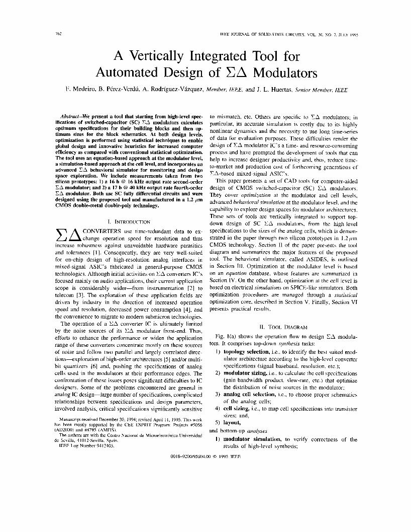
11. TOOL DIAGRAM Fig. I(a) shows the operation flow to design EA modula-
It comprises top-down synthesis tasks: topology selection, i.e., to identify the best suited mod- ulator architecture according to the high-level converter specifications (signal baseband, resolution, etc.); modulator sizing, i.e., to calculate the cell specifications (gain-bandwidth product, slew-rate, etc.) that optimize the distribution of noise sources in the modulator; analog cell selection, i.e., to choose proper schematics of the analog cells; cell sizing, i.e., to map cell specifications into transistor sizes; and, layout,
and bottom-up analyses 1 ) modulator simulation, to verify correctness of the
results of high-level synthesis;
00 I8-9200/95$04.00 0 1995 IEEE
MEDEIRO et al.: A VERTICALLY INTEGRATED M O L FOR AUTOMATED DESIGN OF EA MODULATORS 163
V
Cell Specifications n
Simuluion ok?
V 0 0 0
Optimizer
(b)
Fig. 1 . (a) EA modulator design flow. (b) Proposed tool block diagram.
2) cell simulation, to verify cell synthesis at the electrical
Selection tasks principally involve knowledge issues-the very domain of creative analog designers. Therefore, tools used at this level are oriented to relieve designers of the involved analyses needed to increase knowledge [7]. On the other hand, sizing involves principally optimization is- sues-very well-suited for full automation. With regards to the analyses, cell verification requires electrical simulations (SPICE-like), while those related to high-level synthesis are more conveniently handled through dedicated behavioral sim- ulators, due to the extremely long CPU time needed to iterate electrical simulations at this level.
Fig. l(b) is a flow diagram of the top-down vertical inte- gration of the tools described in this paper with the following main features:
level. *
'Although not shown explicitly in Fig. I(a) for convenience, a final verification step exists, consisting of a single instance of a detailed electrical simulation of the complete extracted layout-very costly in CPU time and memory resources. Consequently, it commonly covers only a few clock cycles, just to check connectivity and evaluate block performance degradation due to unexpected layout-related parasitics.
1) equation-based modulator sizing, 2 ) fast exploration of design parameter space for modula-
tor architecture selection, based on combined equation- based synthesis and optimization,
3 ) dedicated behavioral simulation, bas -d on detailed mod- eling of the building blocks,
4) simulation-based sizing of the analog cells, and 5) optimum global solutions at the different synthesis lev-
els, achieved by the use of statistical optimization tech- niques.
A key block in the proposed tool is the statistical optimiza- tion core, which is invoked for modulator sizing and for cell sizing. Both tasks are formulated by the tool as constrained optimization problems where a number of design objectives (such as power consumption, area occupation, etc.) have to be minimized or maximized subjected to constraints imposed by the requested numerical specification targets (such as 17-b resolution, 20-kHz output rate, dc-gain larger than lo3, etc.). For each case and starting from an initial estimate in the asso- ciated design space, a discrete sequence of movements (repre- sented generically as Az,) is performed until an equilibrium solution point z* is found. The direction and magnitude of these movements are calculated by the statistical optimization core based on the evaluation of a cost function @(z), which quantifies the degree of achievement of the design objectives and the feasibility of the movement taking into account the constraints. For modulator sizing, this cost function, which is formulated automatically by the tool, is evaluated using a library of equations. For cell sizing, it is evaluated through electrical simulation of the cell schematics through a SPICE- like simulator (HSPICE [8] in the prototype version of the tool). Consequently, no supervisory verification of cell sizing is needed-electrical feasibility is guaranteed by construction.
The equations that support high-level synthesis describe the influence of non-idealities of the basic blocks as well as those of purely architectural features, such as integrator weights. This equation database has been conceived to ren- der its expansion simple; the current version includes single- loop low-order and cascaded high-order one-bit, multibit, and pseudomultibit architectures. With regards to the behavioral simulator, it has been specifically designed to consider the different architectures and the non-idealities of the basic cells in the equation database.
111. BEHAVIORAL SIMULATOR In the proposed tool diagram of Fig. l(b), modulator sim-
ulation is the nexus between high-level synthesis and cells synthesis and necessary to validate the results of the modulator sizing optimization. Bear in mind that cells are not yet sized at this level. Thus, two alternatives arise; 1) using macro- models of the cells and conventional electrical simulators and, 2) building dedicated behavioral simulators. Although this election may be somewhat controversial, the accurate estimation of the performance parameters of oversampled data converters requires their simulation over extremely large number of clock cycles, a fact that imposes the second altemative as usual among EA modulator designers [9].

7 64 IEEE JOURNAL OF SOLID-STATE CIRCUITS, VOL. 30. NO. 7, JULY 1995
wpuT , /ln&ator Non-idealities / I
I(?) capacitor effect * K 2-2 Cascade SD Modulator Y
Vin inp d c a . 0 ampl=(-1400 2) frcq=1.25k:
K First Stage -> Znd-order mod. Compl out1 (oi2) real cm: I1 oil (inp.0'0.5 out1,0*0.5:2) real im; I2 oi2 (oil,0*0.5 outl.O'O.5 2) real im;
#Second Stage -> 2nd-order mod CompZ out2 (oi4) real cm; 13 oi3 (oi2.0'0.5 ouQ.0'0.5:2) real im; I4 oi4 (oi3.0'0.5 out2.0*0.5:2) real im;
W Logic for noise cancelation X De13 I4 (outl) full;
Ad4 out (21 15) ideal;
.clock freqd. l2xjitter=lnos~61;
.options fullydiff mismatch;
.output SNR(out) monle=30;
.outpu1 FFr(0ut);
#Models .model im Integrator cunit4.25p cfb=Zp cpa=lp cnl=50u
dcgaindcg dcgnk20 ron=500 npwd=5n sr=SOa gb=25: osp=3 osn=-3;
.model cm Comparator vhigh=l vlow=-1 h y s = 5 h ;
.param dcg = sweep (dec 10 100 IooWO);
(b)
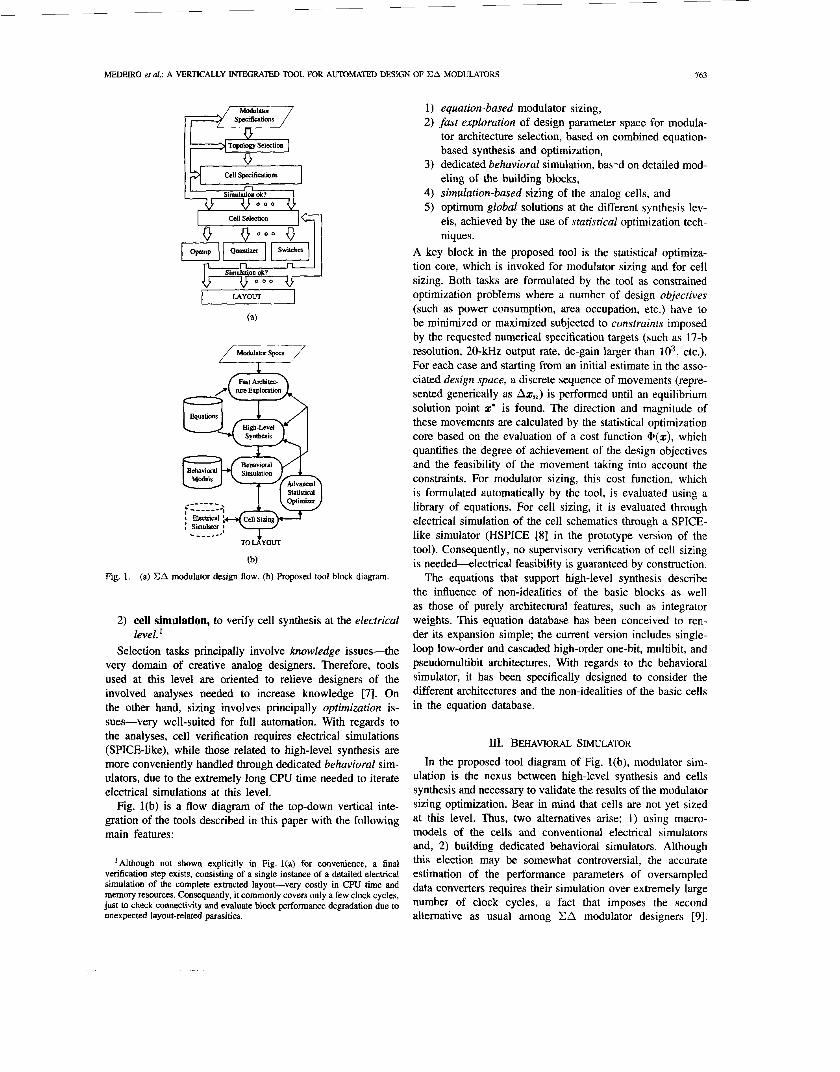
Fig. 2 . (a) Integrator operation flow. (b) Input netlist example.
This has resulted in a few dedicated tools reported already. However, they are either dedicated to a single architecture [ 101 or contemplate only a short catalog of non-idealities [ 111, [ 121. The main difference between our simulator, ASIDES, and other previously reported is that ours is more hardware- oriented. Thus, it covers non-idealities that are critical to design high-performance modulators, such as thermal noise, components mismatch, or the influence of high-order op-amp dynamics, among others.
ASIDES starts from an input netlist containing the modu- lator topology and a list of non-idealities to consider during simulation, and operates in time-domain using functional de- scriptions of the blocks. It generates a time series that is processed using a general-purpose DSP tool, for instance, MATLAB [13] to provide
1) Information about the dynamic performance of the mod- ulator, including the spectrum of the converter out- put, graphs of the signal-to-(noise + distortion) ratio (TSNR), etc.
2) Information about its static performance, through eval- uation of integral non-linearity, offset, gain error, etc.
3) Montecarlo analysis, taking into account fluctuations of both the integrator gains and the terminal specifications of the analog cells. These fluctuations can be indicated by the user or evaluated by the tool on the basis of technological parameters and layout-related variables, for instance, the capacitor size and the partition used in their layout [14]. This capability is especially useful when cascade modulator architectures are considered because of their sensitivity to mismatching [ 151.
4) Parameter sweep, for design space exploration through visualization of the impact of critical design parameters on the modulator performance.
The catalog of building blocks in ASIDES includes voltage sources, integrators, quantizerskomparators, udders, ampli- j ers , preamplijiers, delays, multipliers and generic non-linear blocks. Each is described through a dedicated routine in C- language. To obtain time-series output, these routines are invoked according to the connection specified in the input netlist. Each block output is updated using its present input (and output) and a set of non-idealities related to the electrical implementation included in an associated block model.
Fig. 2(a) illustrates this operation flow for the integrator whose corresponding routine starts a loop that involves the following calculations:
1) Thermal noise originated by the on-re<istance of the switches and integrator op-amps. The equivalent level of white noise is first calculated based on accurate analyti- cal expressions for standard SC multibranch integrators and then added in time-domain to the integrator input using a random number generator.
2 ) Nonlinear scaling and leakage in the integrator due to finite and nonlinear dc-gain of the op-amps.
3) Capacitor non-linearity, represented as a polynomial dependence of the capacitance value on the accumulated voltage.
4) The value of the integrator output voltage is calculated at the end of the settling period. This calculation uses either a linear or non-linear expression of the settling depending on the integrator input, the \lew-rate, gain- bandwidth product (GB), and phase margin of the op- amp, and the integrator gain [16], [17].
5 ) If the output swing of the integrator is surpassed, the output voltage is clipped to that value.
The iterative process shown in Fig. 2(a) is necessary due, on the one hand, to the interdependency between the op-amp dc-gain and the integrator output and, on the other, to the relationship among the capacitor values and their accumulated voltages. However, two or three iterations are commonly sufficient to detect convergence and complete the simulation process. The remaining primitives considered in the behavioral simulator follow descriptions similar to that for the integrator.
Fig. 2(b) shows a typical input netlist; in this case, for a fourth-order 2-2 cascade EA modulator. The input is a pure tone with amplitude varying from -140-0 dBV in 2 dBV steps. The first and second stages are second-order modulators

765 MEDEIRO et al.: A VERTICALLY INTEGRATED TOOL FOR AUTOMATED DESIGN OF CA MODULATORS
01 1
-140 -11 Input Level (dBV)
(b)
_____. /... ..., , .. 125
85 100 -m Opnmp DC-gain
(C)
Fig. 3. Three simulator outputs: (a) Real and ideal case output spectrum for a fourth-order 2-2 cascade EA modulator. (b) SNR versus input amplitude including integrator gain mismatching. (c) SNR for -6 dBV input versus op-amp dc-gain.
composed of two integrators and one comparator. All these elements are of real type and have associated models called “im” for the integrators and “cm” for the comparators. The cancellation logic, whose description is not completely printed, is formed using ideal delays and adders. The clock frequency is set to 5.12 MHz with 1 ns standard deviation jitter and the oversampling ratio is 64. Requested analyses include an FFT of the time series at the output node and the calculation of the signal-to-noise (SNR) curve at this node. They also include a Montecarlo analysis of SNR with the integrator gains as random parameters. Those code lines that start with “model” in Fig. 2(b) are used to specify parameters associated with non- ideal features contemplated in the block models. Note that the op-amp dc-gain is not given a numerical value, but specified through the parameter “dcg”; this is used to sweep a range of dc-gain values-shown in the last command line in Fig. 2(b).
Fig. 3 depicts output provided by the simulator in the case of the netlist of Fig. 2(b), presenting three graphs cor- responding to simulator outputs. The continuous trace in Fig. 3(a) shows the simulated output spectrum, while the
dashed trace shows the corresponding ideal curve. Note the presence of harmonic distortion due to non-linearity of op- amp dc-gain and an unshaped noise floor around -120 dBV mainly due to thermal noise. Fig. 3(b) shows the result of the Montecarlo analysis where all error sources other than mismatch have been disconnected to highlight the influence of the latter. It is of interest to compare the results of Monte Carlo simulation with a calculation of worst-case realized in a single instance of a corresponding equation contained in the equation database used for synthesis. Fig. 3(b) includes this calculated worst-case curve, which coincides with the simulation results. Finally, Fig. 3(c) shows the SNR after decimation as a function of the op-amp dc-gain for -6 dBV @ 5 lcHz input. The continuous trace corresponds to the real case where thermal noise dominates, while the dashed one represents an ideal case (considering only finite dc-gain for the op-amps). Based on the information contained in this graphic, one concludes that a dc-gain of only lo3 suffices to reach maximum performance.
IV. DESIGN EQUATION DATABASE
As mentioned in the description of the tool, equations are the basis for fast architecture exploration and high-level synthesis. Equations supporting the synthesis procedure have been ob- tained through exhaustive analysis of modulator architectures as well as general SC circuits. These equations are grouped into three categories.*
1) Architecture-related equations, to represent quantization noise in connection to the features that affect its shap- ing-integrator leakage, mismatches in integrator gains, non-linearity of the in-loop D-A converter, etc. The analytical expressions covering these phenomena depend on the architecture considered and may be quite different for different topologies; see for instance, [15], [NI, [19].
2) Circuitry-related equations, to represent noise sources
3)
other than quantization noise-thermal noise, noise due to incomplete settling, harmonic distortion due to non- linearity of the integrator gain, etc. For instance, we include here expressions for harmonic distortion at the modulator output due to the op-amp slew-rate and non- linear op-amp dc-gain [ 161; switch on-resistance and op-amp thermal noise [18]; jitter noise [20]; and noise due to incomplete settling of the output signal in the integrators [17]. Since errors due to integrators others than the first are attenuated by the feedback loop of the modulator [I], only these latter are considered for synthesis purposes, which renders the formulation of these errors practically independent of the modulator architecture. On the other hand, slight inaccuracies due to the remaining integrators are evaluated in any case at the phase of behavioral simulation. In addition to these detailed equations, simplified equa- tions have been incorporated to the database. These equations refer to fundamental limits of different topolo- gies and contemplate trade-offs between power con- sumption, resolution, speed, etc., and are addressed to guide modulator selection.
*The full set of equations used for high-level synthesis is found in [27].
IEEE JOURNAL OF SOLID-STATE CIRCUITS. VOL. 30. NO. 7. JULY 1995
E 3 :
s .g
[ -
B
TABLE I NON-IDEALITIES CONSIDERED IN THE To01
-
- - 3rd-order 2-1
Building Blocks (Non-idealities ]Consequences
1
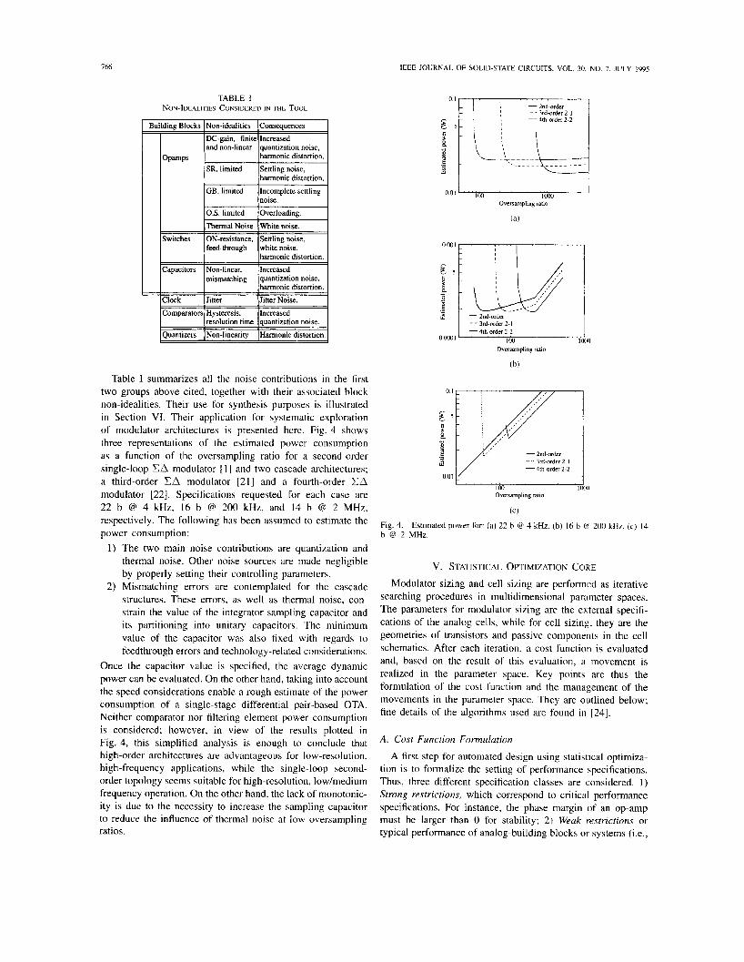
Table I summarizes all the noise contributions in the first two groups above cited, together with their associated block non-idealities. Their use for synthesis purposes is illustrated in Section VI. Their application for systematic exploration of modulator architectures is presented here. Fig. 4 shows three representations of the estimated power consumption as a function of the oversampling ratio for a second-order single-loop EA modulator [ I ] and two cascade architectures; a third-order EA modulator [21] and a fourth-order EA modulator [22]. Specifications requested for each case are 22 b @ 4 kHz, 16 b @ 200 kHz, and 14 b @ 2 MHz, respectively. The following has been assumed to estimate the power consumption:
The two main noise contributions are quantization and thermal noise. Other noise sources are made negligible by properly setting their controlling parameters. Mismatching errors are contemplated for the cascade structures. These errors, as well as thermal noise, con- strain the value of the integrator sampling capacitor and its partitioning into unitary capacitors. The minimum value of the capacitor was also fixed with regards to feedthrough errors and technology-related considerations.
Once the capacitor value is specified, the average dynamic power can be evaluated. On the other hand, taking into account the speed considerations enable a rough estimate of the power consumption of a single-stage differential pair-based OTA. Neither comparator nor filtering element power consumption is considered; however, in view of the results plotted in Fig. 4, this simplified analysis is enough to conclude that high-order architectures are advantageous for low-resolution, high-frequency applications, while the single-loop second- order topology seems suitable for high-resolution, low/medium frequency operation. On the other hand, the lack of monotonic- ity is due to the necessity to increase the sampling capacitor to reduce the influence of thermal noise at low oversampling ratios.
- 2nd-order - - 3rdmder 2-1 - 4th-order 2-2
0. I
. - _ _ _ _ _ _ _ _ _ - - - - -
I I
i;i
loo0 0.01 .
Oversampling ratio
(a)
0.001 I 1
- 4ih~rder 2-2 100 IKKI O o o o l
Oversampling ram
(b)
0.1
s3 E g 3 1 E
0.01
- 2nd-order - - - - 3rd-order2-I - 4th-order 2-2
I I Ovenampling 100 rauo loo0
(C)
Fig 4 b @ 2 MHz.
Estimated power for (a) 22 b @ 4 kHz. (b) 16 b CQ 200 kHz (c) 14
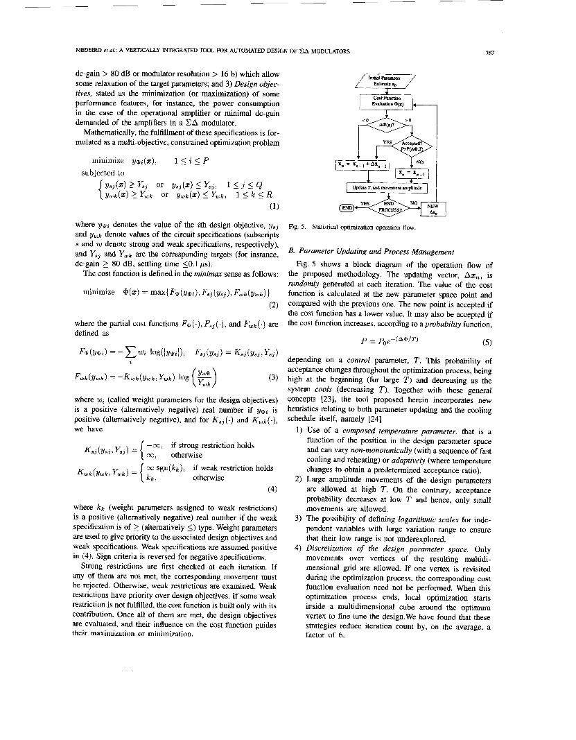
v. STATISTICAL OPTIMIZATION COKE
Modulator sizing and cell sizing are performed as iterative searching procedures in multidimensional parameter spaces. The parameters for modulator sizing are the extemal specifi- cations of the analog cells, while for cell sizing, they are the geometries of transistors and passive components in the cell schematics. After each iteration, a cost function is evaluated and, based on the result of this evaluation, a movement is realized in the parameter space. Key points are thus the formulation of the cost function and the management of the movements in the parameter space. They are outlined below; fine details of the algorithms used are found in 1241.
A. Cost Function Formulation
A first step for automated design using statistical optimiza- tion is to formalize the setting of performance specifications. Thus, three different specification classes are considered. 1) Strong restrictions, which correspond to critical performance specifications. For instance, the phase margin of an op-amp must be larger than 0 for stability; 2) Weak restrictions or typical performance of analog-building blocks or systems (i.e.,
MEDEIRO et al.: A VERTICALLY INTEGRATED TOOL FOR AUTOMATED DESIGN OF EA MODULATORS
dc-gain > 80 dB or modulator resolution > 16 b) which allow some relaxation of the target parameters; and 3 ) Design objec- tives, stated as the minimization (or maximization) of some performance features, for instance, the power consumption in the case of the operational amplifier or minimal dc-gain demanded of the amplifiers in a EA modulator.
Mathematically, the fulfillment of these specifications is for- mulated as a multi-objective, constrained optimization problem
minimize y,pi(z), 1 5 i I P subjected to
2 Y3j or ySj(z) I Ysj, 1 Ij L Q 2 ywk Or Ywk(Z) I Ywk, 15 k 5 R
(1)
where y,pi denotes the value of the ith design objective, ysj and 2/wk denote values of the circuit specifications (subscripts s and w denote strong and weak specifications, respectively), and Ysj and Ywk are the corresponding targets (for instance, dc-gain 2 80 dB, settling time 50.1 ,us).
The cost function is defined in the minimax sense as follows:
where the partial cost functions F,p (.), Fsj (.), and F,I, (.) are defined as
(3)
where wi (called weight parameters for the design objectives) is a positive (alternatively negative) real number if y ~ i is positive (alternatively negative), and for K3j (-) and &k('), we have
-CQ, if strong restriction holds CO, otherwise
00 sgn(kk), if weak restriction holds { k k , otherwise Kwk(Ywk, ywk) =
(4)
where k k (weight parameters assigned to weak restrictions) is a positive (alternatively negative) real number if the weak specification is of 2 (alternatively 5) type. Weight parameters are used to give priority to the associated design objectives and weak specifications. Weak specifications are assumed positive in (4). Sign criteria is reversed for negative specifications.
Strong restrictions are first checked at each iteration. If any of them are not met, the corresponding movement must be rejected. Otherwise, weak restrictions are examined. Weak restrictions have priority over design objectives. If some weak restriction is not fulfilled, the cost function is built only with its contribution. Once all of them are met, the design objectives are evaluated, and their influence on the cost function guides their maximization or minimization.
Evaluation Yx)
& AYx)?
1
Fig. 5. Statistical optimization operation flow.
B. Parameter Updating and Process Management
Fig. 5 shows a block diagram of the operation flow of the proposed methodology. The updating vector, Az,, is randomly generated at each iteration. The value of the cost function is calculated at the new parameter space point and compared with the previous one. The new point is accepted if the cost function has a lower value. It may also be accepted if the cost function increases, according to a probability function,
depending on a control parameter, T. This probability of acceptance changes throughout the optimization process, being high at the beginning (for large T ) and decreasing as the system cools (decreasing 7'). Together with these general concepts [23], the tool proposed herein incorporates new heuristics relating to both parameter updating and the cooling schedule itself, namely [24]
1) Use of a composed temperature parameter, that is a function of the position in the design parameter space and can vary non-monotonically (with a sequence of fast cooling and reheating) or adaptively (where temperature changes to obtain a predetermined acceptance ratio).
2) Large amplitude movements of the design parameters are allowed at high T. On the contrary, acceptance probability decreases at low T and hence, only small movements are allowed.
3) The possibility of defining logarithmic scales for inde- pendent variables with large variation range to ensure that their low range is not underexplored.
4) Discretization of the design parameter space. Only movements over vertices of the resulting multidi- mensional grid are allowed. If one vertex is revisited during the optimization process, the corresponding cost function evaluation need not be performed. When this optimization process ends, local optimization starts inside a multidimensional cube around the optimum vertex to fine tune the design.We have found that these strategies reduce iteration count by, on the average, a factor of 6.

768
DPTIMIZED SPECS FOR Modulator Topology
Sampling frequency (MHz) Oversampling ratio Differential reference voltage E (V)
[ntegralors Sampling capacitor C, (pF) Feed-back capacitor CO (pF) Unitary capacitance (pF) MOS switch-ON resistance (kn) Maximum clock iitter Ins)
IEEE JOURNAL OF SOLID-STATE CIRCUITS. VOL. 30, NO. 7, JULY 1995
16bit@16&@ 17bit@40kHz f1.5V @*1.5V Second-order Cascade 2-2 4.096 5.12 256 128
0.75 0.75 1 .o I .o 2.0 2.0
>= 0.25
<= 1.0 <= 1.0 <= 3.0 <=fly
-E
(b)
Fig. 6 . (a) Second-order single-loop YA modulator. (b) Fourth-order two-stage EA modulator.
VI. PRACTICAL RESULTS
The use of the proposed tool is illustrated through fully- differential SC realizations of the second-order modulator of Fig. 6(a) [ 11 and the fourth-order chopper-compensated two- stage modulator of Fig. 6(b) [22]. They have been designed to achieve 16 b @ 16 kHz output rate and 17 b '2 40 kHz output rate, respectively, in a 1.2 pm; n-well double-poly double- metal CMOS technology. For both cases, high-level synthesis and cell sizing were realized automatically by the tool, while layout was manual.
Table I1 displays the outcome of high-level synthesis for both structures. This is already in the format provided by the high-level synthesis tool, which also summarizes the different noise contributions anticipated by the equations for the completed design-displayed at the bottom in Table 11. The associated statistical optimization procedures required 10 000 iterations for the second-order modulator and 30 000 iterations for the fourth-order modulator and lasted 5 s CPU time and 11.8 s CPU time, respectively, on a 100 MIP's workstation. These short CPU times are a positive consequence of using equations and render the ability to explore design spaces through iterations of the optimum high-level synthesis procedure. For both architectures, the sampling capacitor was fixed to a relatively small value to evaluate the ability of the procedure to obtain feasible designs in spite of a relatively large thermal noise contribution. In particular, the thermal noise contributed by a sampling capacitor of 1 pF is at the very border of feasibility for the fourth-order modulator (see the bottom part of Table 11). In this sense, the summary of noise contributions reported at the bottom of the high-level
TABLE I1 HIGH-LEVEL SYNTHESIS TOOL OUWUT
GB (MH4 >= 18.0 >= 15.3 Slew-rate ('//us) >E 50.0 >= 57.35 Total output swing (V) >= 6.0 >= 6.0
RESOLUTION & NOISE POWER CONTRIBUTIONS
lhermal noise (dB) -100.0 -104.3
Incomplete settling noise (dB) -1449 -177.7
litter noise (dB) -109.5 -111.2
synthesis report is of interest to guide design exploration if specifications are not met and a new iteration of the high-level -
" synthesis procedure is required.
MEDEIRO et al.: A VERTICALLY INTEGRATED TOOL FOR AUTOMATED DESIGN OF EA MODULATORS 769
(b)
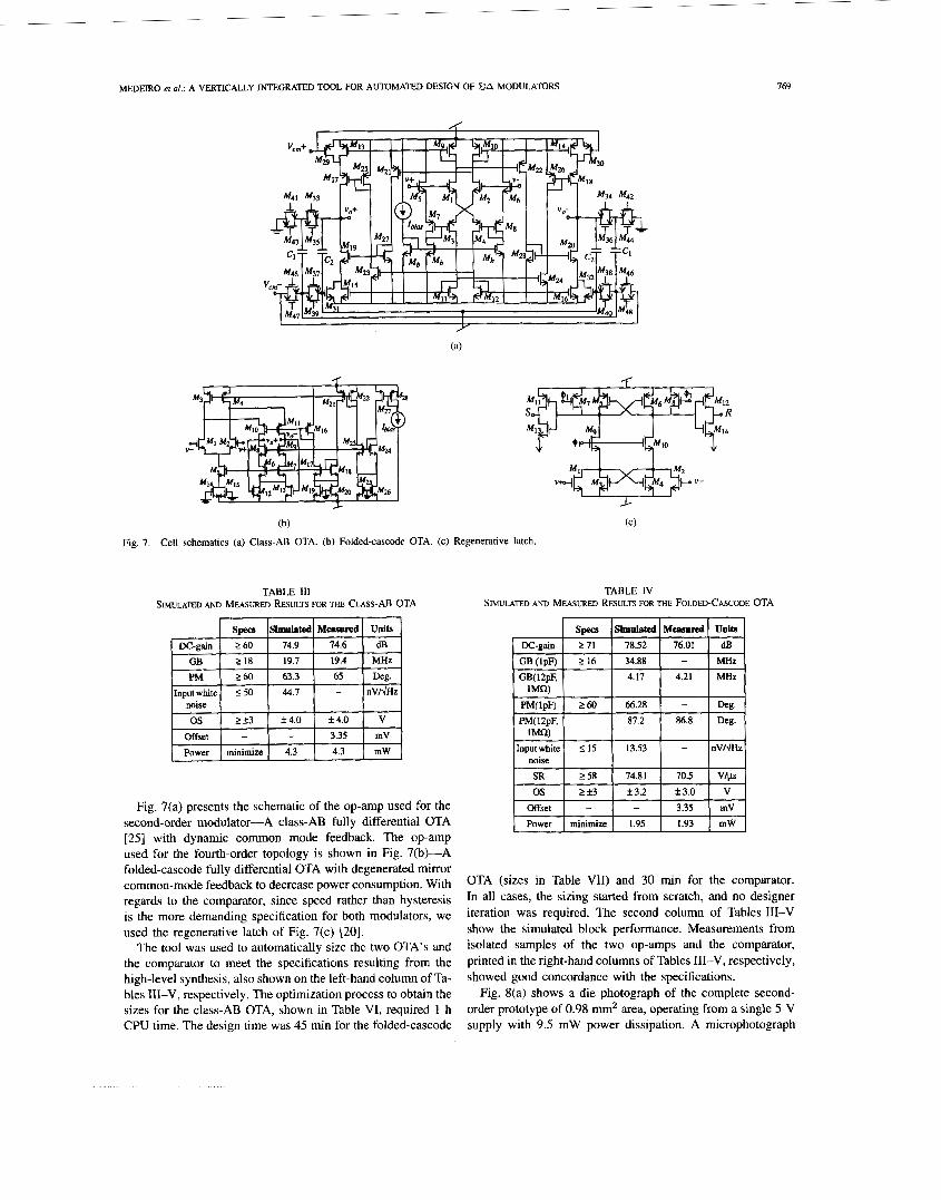
Fig. 7. Cell schematics (a) Class-AB OTA. (b) Folded-cascode OTA. (c) Regenerative latch,
U
TABLE III SWULATED AND MEASURED RESULTS FOR THE CLASS-AB OTA
Fig. 7(a) presents the schematic of the op-amp used for the second-order modulator-A class-AB fully differential OTA [25] with dynamic common mode feedback. The op-amp used for the fourth-order topology is shown in Fig. 7(b)-A folded-cascode fully differential OTA with degenerated mirror common-mode feedback to decrease power consumption. With regards to the comparator, since speed rather than hysteresis is the more demanding specification for both modulators, we used the regenerative latch of Fig. 7(c) [20].
The tool was used to automatically size the two OTA’s and the comparator to meet the specifications resulting from the high-level synthesis, also shown on the left-hand column of Ta- bles 111-V, respectively. The optimization process to obtain the sizes for the class-AB OTA, shown in Table VI, required 1 h CPU time. The design time was 45 min for the folded-cascode
TABLE IV SIMULATED AND MEASURED RESULTS FOR THE FOLDED-CASCODE OTA
W l p Q 260 66.28 Deg. -
PM( 12pF, 87.2 86.8 Deg.
OTA (sizes in Table VII) and 30 min for the comparator. In all cases, the sizing started from scratch, and no designer iteration was required. The second column of Tables 111-V show the simulated block performance. Measurements from isolated samples of the two op-amps and the comparator, printed in the right-hand columns of Tables 111-V, respectively, showed good concordance with the specifications.
Fig. 8(a) shows a die photograph of the complete second- order prototype of 0.98 mm2 area, operating from a single 5 V supply with 9.5 mW power dissipation. A microphotograph

770 IEEE JOURNAL OF SOLID-STATE CIRCUITS, VOL. 30, NO. 7. JULY 1995
TABLE V SIMULATED AND MEASURED RESULTS FOR THE C
36.4
Offset 22.5
TABLE VI SIZES FOR THE CLASS-AB OTA
MI,? 149.2J2.2 pdpm M21,22 4822.2
M3.4 2212.2 M23.24 42.812.2
Mg.6 80.4/2.2 M25.26 6.u2.2
M7.8 11.8i2.2 M27.28 5.4J2.2
"
''
"
MPARATOR
Units
mV
mV
TABLE VI1 SIZES FOR THE FOLDED-CASCODE OTA
of the fourth-order prototype with 0.94 mm2 area and power consumption of 10 mW @ 5 V is shown in Fig. 8(b). To evaluate the performance of the two modulators, a test board was fabricated following the indications in [26] to reduce capacitive and inductive coupling. The modulator input was provided using a high-quality differential sinusoidal signal source (less than -100 dB THD) through a simple passive low-pass filter to prevent aliasing. The output series were acquired with an HP82000 unit and transferred to a worksta- tion for processing. The cancellation logic of the fourth-order modulator, as well as the decimation digital filters, were implemented on a workstation using the same signal processor as used for simulations.
Fig. 9(a) presents the baseband spectrum of the second- order prototype obtained through an FFT of 65 536 consecutive output samples. The input was a sinewave of 2 kHz frequency and -6 dBV amplitude, the reference voltage was f 1 . 5 V,
(b)
Fig. 8. two-stage YA modulator.
Die photographs (a) Second-order EA modulator. tb) Fourth-order
and the sampling frequency was fixed to 4.096 MHz. The small harmonic components in the spectrum can be attributed to deficiencies of the test board, since the distortion was very sensitive to changes in the grounding configuration and decoupling capacitors.
The output spectrum of the fourth-order prototype for -9 dBV 0 4 kHz input tone sampled at 5.12 MHz is shown in Fig. 9(b) and compared to the output spectrum of its first stage, a second-order modulator. Differences between the two noise-shaping functions are visible. However, the baseband of the fourth-order modulator is dominated by unshaped thermal noise. Our simulations show that this phenomena can be explained taking into account that the input noise power spectral density of the folded-cascode op-amp was larger than expected. Fig. 10 presents the SNR of the fourth-order modulator as a function of the input level for five values of the oversampling ratio; 128 (nominal value), 64. 32, 16, and 8, which lead to 40, 80, 160, 320, and 640 kHz digital output rate, respectively. Note that for low oversampling ratios, the quantization noise dominates and, consequently. the distances

MEDEIRO er al.: A VERTICALLY INTEGRATED TOOL FOR AUTOMATED DESIGN OF EA MODULATORS 77 1
Fig. 9. totype.
Output spectrums (a) Second-order prototype. (b) Fourth-order pro-
Fig. IO. for five values of the oversampling ratio.
SNR of the fourth-order prototype as a function of the input level
TABLE VI11 PERFORMANCE OF THE SECOND-ORDER MODULATOR
Oversampling Ratio Resolution
%.3dB SNR-peak
Area (without pads) I 0.98 mm2
between the maxima of the corresponding SNR curves are in concordance with the theoretic value of 27 dB. On the other hand, for large oversampling ratio, the dominant source of noise is not quantization, but thermal noise, which reflects in smaller separations among the SNR curves. Summarized performance of both modulators are shown in Tables VI11 and IX.
TABLE IX PERFORMANCE OF THE FOURTH-ORDER EA MODULATOR
OversamplingRatio I 128 1 64 I 32 1 16 I 8 Resolution I 16.7 I 15.5 I 14.8 I 11 I 6.5
As a concluding remark, it is worth mentioning that the concourse of this tool enabled us to complete a full- custom design of the fourth-order modulator with an effort of only 3 madweek, of which 65% was devoted to the layout phase-the only part performed manually. Hence, the proposed methodology can be considered as a valid realization in the concept of automated design of high-resolution analog systems.
REFERENCES
J. C. Candy and G. C. Temes, Oversampling Delta-Sigma Converters. Piscataway, NI: IEEE Press, 1992. B. P. Del Signore, D. A. Kerth, N. S. Sooch, and E. J. Swanson, “A monolithic 20-b Delta-Sigma A/D converter,” IEEE J. Solid-state Circuits, vol. 25, pp. 1311-1317, Dec. 1990. G. Yin and W. Sansen, “A high-frequency and high-resolution fourth- order EA A/D converter in Bi CMOS technology,” IEEE J. Solid-state Circuits, vol. 29, pp. 857-865, Aug. 1994. Y. Matsuya and J. Yamada, “1 V power supply, 384 ks/s I O b A/D and D/A converters with swing-suppression noise shaping,” in Proc. IEEE Int. Solid-state Circuits Con$, 1994, pp. 192-193. T. Ritoniemi, “High-speed 1 bit CA-modulators,” in Workrhop on Advances in Analog Circuit Design, Delft, Apr. 1992, pp. 191-203. G. C. Temes and B. Leung, “EA data converter architectures with multibit internal quantizers,” in Pmc. 11th European Conf Circuit Theory Design, H. Dedieu, Ed., Davos, 1993, vol. 2, pp. 1613-1618. G. Gielen and W. Sansen, Symbolic Analysis for Automared Design of Analog Circuits. Boston: Kluwer, 1991. HSPICE: User’s Manual, Meta Software Inc., 1988. V. F. Dias, V. Liberali, and F. Maloberti, “Design tools for oversampled data converters: Needs and solutions,” Micmelecrronics J . . vol. 23, pp. 6 4 4 5 0 , 1992. S. R. Norsworthy, I. G. Post, and H. S. Fetterman: “A 14 bit 80 kHz Sigma-Delta A/D converter: Modeling, design and performance evaluation,” IEEE J . Solid-State Circuits, vol. 24, pp. 25&266, Apr. 1989. C. H. Wolff and L. Carley, “Simulation of A-Y modulators using behavioral models,” in Proc. ISCAS’90, 1990, pp. 376-379. V. F. Dias, V. Liberali, and F. Maloberti, “TOSCA: A user-friendly behavioral simulator for oversampling A/D converters,” in Pmc.
MATLAB: User’s Guide, The Mathworks Inc., 1991. J.-B. Shyu, G. Temes, and F. Krummenacher, “Random error effects in matched MOS capacitors and current sources,” IEEE J. Solid-state Circuits, vol. SC-19. pp. 948-955, Dec. 1984. D. B. Ribner, “A comparison of modulator networks for high-order oversampled XA analog-to-digital converters,” IEEE Trans. Circuits Syst., vol. 38, pp. 145-159, Feb. 1991. F. Medeiro, B. Perez-Verdli. A. Rodriguez-VBzquez, and J. L. Huertas, “Modeling opamp-induced harmonic distortion for switched-capacitor Sigma-Delta modulator design,” in Proc. ISCAS’94, London, June 1994, vol. 5, pp. 445448. V. F. Dias, G. Palmisano, P. O’Leary, and F. Maloherti, “Fundamental limitations of switched-capacitor Sigma-Delta modulators,” IEE PROC. - G, vol. 139, pp. 27-32, Feb. 1992.
ISCAS’91, 1991, pp. 2677-2680.

112 IEEE JOURNAL OF SOLID-STATE CIRCUITS, VOL. 30, NO. 7, JULY 1995
[I81 F Medeiro, B PCrez-Verdu, A. Rodriguez-Vazquez, and J L Huertas, “Design consideration for a fourth-order switched-capacitor Sigma-Delta modulator,” in Pmc 11th European Conf Circuit Theorv Design, H Dedieu, Ed., Davos, 1993. vol 2, pp 1607-1612
[I91 B F Brandt and B A Wooley, “A 50 MHz multibit EA modulator for 12 b 2 MHz A/D conversion,” IEEEJ Solid-State Cixuitr, vol. 26, pp 1746-1756, Dec 1991
[20] B E Boser and B. A Wooley, “The design of Sigma-Delta modulation analog-to-digital converters,” ZEEE J Solid-Stare Circuits, vol 23 pp 1298-1308, Dec 1988 network modeling
[21] L A Williams, 111 and B. A Wooley, “Third-order cascaded EA modulators.” IEEE Truns Circuits Svst., vol 38, pp. 489498, May 1991
[22] H Baher and E Afifi. “Novel fourth-order Sigma-Delta convertor,”
B. Phz-Verdli was born in Monovar, Spain She received the Licenciado en Fisica degree in 1979 and the Doctor en Ciencias Fisicas degree in 1985, both from the University of Seville, Spain
Since October 1978, she has been with the De- partment of Electronics and Electromagnetism at the University of Seville, where she IS employed as an Associate Professor Her research interest lies in the fields of analog/digital circuit design and nonlinear
r231
1241
Electron. Lerr., vol. 28, pp. 1437-1438, July 1992. P. J . M. van Laarhoven and E. H. L. Aarts, Simulared Annealing; Theor?; and Applicutions. Boston: Kluwer, 1987. F. Medeiro. R. Rodriguez-Macpas, F. V. Fernandez, R. Dominguez- Castro, J. L. Huertas. and A. Rodriguez-Vizquez, “Global design of analog cells using statistical optimization techniques.” Analog Inregrated Circuirs Signal Process., vol. 6, pp. 179-195. Nov. 1994. R. Castello and P. Gray, “A high-performance micropower switched- capacitor filter,” IEEE J. Solid-State Circuits, vol. SC-20, pp. 1122-1132, Dec. 1985. J . L. LaMay and H. J . Bogard, “How to obtain maximum practical performance from state-of-the-art Delta-Sigma analog-to-digital convert- ers,’’ IEEE Truns. Insrrument. Measure., vol. 41, pp. 861-867, Dec. 1992. F. Medeiro, B. Perez-Verdli, and A. Rodriguez-Vazque7, “Behavioral modeling of X I modulators for optimum high-level synthesis,’’ Internal Report, Centro Nacional de Microelectr6nica. Sevilla 1994.
F. Medeiro was born in Higuera de Vargas, Spain. He received the Licenciado en Fisica degree in 1990 from the University of Seville, Spain.
He is currently working towards the Ph.D. degree in the field of modeling and automated design of SD converters. Since 1991, he has been working at the Department of Analog Circuit Design of the Centro Nacional de Microelectronica. His research interests include mixed-mode integrated circuit design and design automation.
A. Rodriguez-Vhzquez (M’91) w l t ~ bom in Seville, Spain He received the Licenciado en Fisica degree in 1977 and the Doctor en Ciencias Fisicas degree in 1983, both from the Universitj of Seville, Spain.
Since 1978, he has been with the Department of Electronic\ and Electromagnetism at the University of Seville, uhere he is a Full Professor He is also with the Department of Analog Circuit Design of the Centro Nacional de Microelectronica His research interests are in analog VLSI, including neural, fuzzy, and chaotic circuit\. mixed-mode IC
design and computer-aided design and modeling of analog integrated circuits. He ha$ published 45 journal papers, approximately 90 conference papers, and several book chapters
Dr Rodriguez-Vazquez has been an Associate Editor of IEEE
’
TRAhSACTlONS ON CIRCUITS A h D SYSTEMS since June 1993
J. L. Huertas (M’7&SM’91) wa\ born in Seville, Spain He received the Licenciado en Fisica degree in 1969 and the Doctor en Cienci,is Fisicas degree in 1973, both from the University of Seville, Spain.
From 1970 to 1971, he waq with the Philips Intemational Institute, Eindhoven. The Netherlands, as a postgraduate \tudent Since 1971, he has been with the Department of Electronics and Electro- magnetism at the Univer\ity of Seville, where he is a Full Professor He is also the Director of the Deuartment of Analoe Circuit De\ien of the Centro
Nacional de Microelectronica. His research interests are in the fields of multivalued logic, sequential machines, analog circuit design, and nonlinear network analysis and synthesis.