TPGS-based and S-thanatin functionalized nanorods ... - Nature
Upload
independentCategory
view
0download
0
ARTICLE IN PRESS
0022-0248/$ - se
doi:10.1016/j.jcr
�Correspondifax: +8263 270
E-mail addre
Journal of Crystal Growth 282 (2005) 131–136
www.elsevier.com/locate/jcrysgro
Catalyst-free large-quantity synthesis of ZnO nanorods by avapor–solid growth mechanism: Structural and optical
properties
A. Umar, S.H. Kim, Y.-S. Lee, K.S. Nahm, Y.B. Hahn�
School of Chemical Engineering and Technology and Nanomaterials Research Centre, Chonbuk National University, Chonju 561-756,
Republic of Korea
Received 28 March 2005; accepted 27 April 2005
Available online 13 June 2005
Communicated by R. Kern
Abstract
The formation of high-density ZnO nanorods has been achieved by a vapor–solid growth mechanism using metallic
zinc powder and oxygen gas as source materials for zinc and oxygen, respectively. General morphological studies
indicated that the as-grown products are flower-shaped containing several hundreds of nanorods. The obtained
nanorods have a diameter of 150–250 nm while their lengths are 5–10 mm. The detailed structural analysis revealed thatthe ZnO nanorods exhibit a single crystalline wurtzite hexagonal structure and preferentially oriented in the c-axis
direction. Room temperature Raman scattering and photoluminescence studies found that the as-grown ZnO nanorods
have good crystal quality with the hexagonal wurtzite phase containing very less structural defects.
r 2005 Elsevier B.V. All rights reserved.
PACS: 68.65.+g; 78.55.Et; 78.66.Hf
Keywords: A1. High-resolution transmission electron microscopy; A1. Optical characterization; A1. ZnO nanorods; A2. Vapor–solid
mechanism
1. Introduction
A highly applicable and widely used II–VIsemiconducting material, ZnO, with a wide band
e front matter r 2005 Elsevier B.V. All rights reserve
ysgro.2005.04.095
ng author. Tel.: +8263 270 2439;
2306.
ss: [email protected] (Y.B. Hahn).
gap (3.37 eV) and high exciton binding energy(60meV) is an excellent candidate for the fabrica-tion of nanoelectronic and photonic devices [1,2].Because of its wide band gap and high excitonbinding energy much larger than ZnSe (22meV)and GaN (25meV), it has an opportunity torecognize itself as a versatile material and con-siderably acknowledged because of its catalytic,
d.
ARTICLE IN PRESS
A. Umar et al. / Journal of Crystal Growth 282 (2005) 131–136132
electrical, optoelectronic, and photochemicalproperties [3–6]. It is known that exciton bindingenergy must be much greater than the thermalenergy at room temperature to show the efficientexciton laser action at room temperature. So thelow threshold intensity, high chemical stability andlow growth temperature make the ZnO a nicecandidate for room temperature UV lasing [7–10].Due to the aforementioned fields and applications,needless to say, the hexagonal wurtzite ZnO couldbe one of most important materials for futureresearch and applications. A wide variety of ZnOnanostructures have been synthesized by thevarious fabrication techniques and are reportedin the literature till date [11–20].In this paper, we report the catalyst-free large-
scale synthesis of ZnO nanorods grown by thethermal evaporation method using a rapid thermalreactor, in which the required temperatures areattainable in a short time. High-purity, commer-cially available zinc powder and oxygen gas wereused as source materials for the zinc and oxygen,respectively. Furthermore, the structural andoptical properties of the deposited ZnO nanorodswere studied in detail.
2. Experimental details
The synthesis of high-density ZnO nanorodswas carried out by the rapid thermal, chemicalvapor deposition process, which contains a hor-izontal quartz tube furnace with the halogen lampheating system having the heating rate of 10 1C/s.A high-purity metallic Zn powder (99.99%) andoxygen gas (99.999%) have been used as precur-sors of Zn and oxygen, respectively. The sourcematerial, metallic zinc powder, was put into aquartz boat and loaded inside the quartz tubefurnace. Nitrogen gas (99.999%) was used as acarrier gas and to create an inert atmosphere insidethe furnace during the whole reaction process.Before starting the reaction, the chamber pressurewas lowered to 3Torr using a rotary vacuumpump, which was slightly increased after theintroduction of the reactant gases. The sourcematerial, metallic zinc powder, was rapidly heatedup to the temperature ranges 500–620 1C under a
flow of high-purity nitrogen carrier gas with a flowrate of 10 sccm (standard cubic centimeter perminute). When the furnace temperature reachedthe desired growth temperature, the oxygen gaswas flowed at 20 sccm during the whole growthperiod. The typical growth time for the synthesisof these ZnO nanorods was 1–1.5 h. After thegrowth process, the white colored products weredeposited near the outlet of the quartz tube. Theseproducts were scratched from the quartz tube andexamined in terms of structural and opticalproperties.General morphology of the deposited ZnO
nanorods was observed using the scanning elec-tron microscopy (SEM) while the detailed struc-tural characterization was done by thetransmission electron microscope (TEM) equippedwith the selected area electron diffraction (SAED)patterns. The crystallinity and crystal phase of thedeposited structures were investigated by X-raydiffraction (XRD) pattern measured with Cu-Karadiation. The room temperature Raman scatter-ing and photoluminescence (PL) spectroscopy withthe Ar+ (513.4 nm) and He–Cd (325 nm) laser lineas the exciton sources, respectively, were used toexamine the optical properties of the as-grownZnO nanorods.
3. Results and discussions
3.1. Structural characterization and growth
mechanism of the synthesized high-density
catalyst-free ZnO nanorods
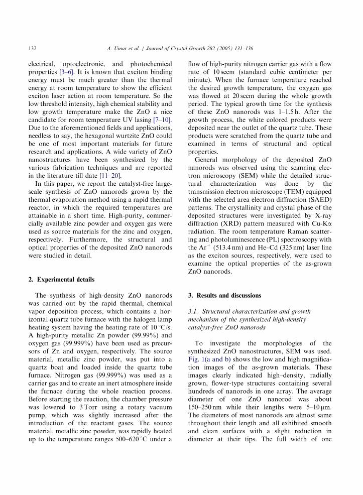
To investigate the morphologies of thesynthesized ZnO nanostructures, SEM was used.Fig. 1(a and b) shows the low and high magnifica-tion images of the as-grown materials. Theseimages clearly indicated high–density, radiallygrown, flower-type structures containing severalhundreds of nanorods in one array. The averagediameter of one ZnO nanorod was about150–250 nm while their lengths were 5–10 mm.The diameters of most nanorods are almost samethroughout their length and all exhibited smoothand clean surfaces with a slight reduction indiameter at their tips. The full width of one
ARTICLE IN PRESS
Fig. 1. Low (a) and high (b) magnified SEM images of ZnO
nanorods synthesized using metallic zinc powder and oxygen
gas as source materials for zinc and oxygen, respectively.
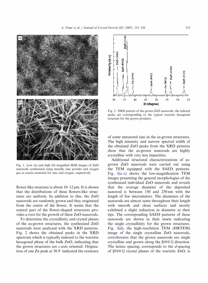
Fig. 2. XRD pattern of the grown ZnO nanorods: the indexed
peaks are corresponding to the typical wurtzite hexagonal
structure for the grown products.
A. Umar et al. / Journal of Crystal Growth 282 (2005) 131–136 133
flower-like structure is about 10–12 mm. It is shownthat the distributions of these flowers-like struc-tures are uniform. In addition to this, the ZnOnanorods are randomly grown and they originatedfrom the centre of the flower. It seems that thecentral part of the flower-shaped structures pro-vides a root for the growth of these ZnO nanorods.To determine the crystallinity and crystal planes
of the as-grown structures, the synthesized ZnOnanorods were analyzed with the XRD patterns.Fig. 2 shows the obtained peaks in the XRDspectrum which is typically indexed to the wurtzitehexagonal phase of the bulk ZnO, indicating thatthe grown structures are c-axis oriented. Origina-tion of one Zn peak at 38.91 indicated the existence
of some unreacted zinc in the as-grown structures.The high intensity and narrow spectral width ofthe obtained ZnO peaks from the XRD patternsshow that the as-grown nanorods are highlycrystalline with very less impurities.Additional structural characterizations of as-
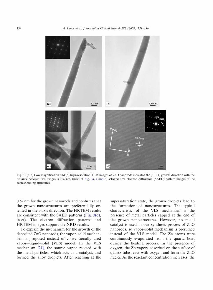
grown ZnO nanorods were carried out usingthe TEM equipped with the SAED patterns.Fig. 3(a–c) shows the low-magnification TEMimages presenting the general morphologies of thesynthesized individual ZnO nanorods and revealsthat the average diameter of the depositednanorod is between 150 and 250 nm with thelength of few micrometers. The diameters of thenanorods are almost same throughout their lengthwith smooth and clean surfaces and mostlyexhibited a slight reduction in diameter at theirtips. The corresponding SAED patterns of thesenanorods are shown in their insets indicatingthe single crystallinity for the grown structures.Fig. 3(d), the high-resolution TEM (HRTEM)image of the single crystalline ZnO nanorods,corroborates that the grown nanorods are singlecrystalline and grown along the [0 0 0 1] direction.The lattice spacing, corresponds to the d-spacingof [0 0 0 1] crystal planes of the wurtzite ZnO, is
ARTICLE IN PRESS
Fig. 3. (a–c) Low magnification and (d) high-resolution TEM images of ZnO nanorods indicated the [0 0 0 1] growth direction with the
distance between two fringes is 0.52 nm, (inset of Fig. 3a, c and d) selected area electron diffraction (SAED) pattern images of the
corresponding structures.
A. Umar et al. / Journal of Crystal Growth 282 (2005) 131–136134
0.52 nm for the grown nanorods and confirms thatthe grown nanostructures are preferentially or-iented in the c-axis direction. The HRTEM resultsare consistent with the SAED patterns (Fig. 3(d),inset). The electron diffraction patterns andHRTEM images support the XRD results.To explain the mechanism for the growth of the
deposited ZnO nanorods, the vapor–solid mechan-ism is proposed instead of conventionally usedvapor-–liquid–solid (VLS) model. In the VLSmechanism [21], the source vapor reacted withthe metal particles, which acts as a catalyst, andformed the alloy droplets. After reaching at the
supersaturation state, the grown droplets lead tothe formation of nanostructures. The typicalcharacteristic of the VLS mechanism is thepresence of metal particles capped at the end ofthe grown nanostructures. However, no metalcatalyst is used in our synthesis process of ZnOnanorods, so vapor–solid mechanism is presumedinstead of the VLS model. The Zn atoms werecontinuously evaporated from the quartz boatduring the heating process. In the presence ofoxygen, the Zn vapors adsorbed on the surface ofquartz tube react with oxygen and form the ZnOnuclei. As the reactant concentration increases, the
ARTICLE IN PRESS
A. Umar et al. / Journal of Crystal Growth 282 (2005) 131–136 135
ZnO nuclei individually grow in upward directionin the form of nanorods. The ZnO nanorods aregrown along the [0 0 0 1] direction which wassubstantiating from the HRTEM image andSAED patterns (Fig. 3(d)).
3.2. Optical properties of synthesized high- density
catalyst-free ZnO nanorods
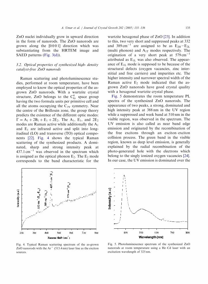
Raman scattering and photoluminescence stu-dies, performed at room temperature, have beenemployed to know the optical properties of the as-grown ZnO nanorods. With a wurtzite crystalstructure, ZnO belongs to the C46v space grouphaving the two formula units per primitive cell andall the atoms occupying the C3V symmetry. Nearthe centre of the Brillouin zone, the group theorypredicts the existence of the different optic modes:G ¼ A1 þ 2B1 þ E1 þ 2E2: The A1, E1, and 2E2modes are Raman active while additionally the A1and E1 are infrared active and split into long-itudinal (LO) and transverse (TO) optical compo-nents [22]. Fig. 4 shows the typical Ramanscattering of the synthesized products. A domi-nated, sharp and strong intensity peak at437.1 cm�1 was observed in the spectrum whichis assigned as the optical phonon E2. The E2 modecorresponds to the band characteristic for the
Fig. 4. Typical Raman scattering spectrum of the as-grown
ZnO nanorods with the Ar+ (513.4 nm) laser line as the exciton
sources.
wurtzite hexagonal phase of ZnO [23]. In additionto this, two very short and suppressed peaks at 332and 389 cm�1 are assigned to be as E2H2E2L(multi phonon) and A1T modes respectively. Theorigination of a very short peak at 579 cm�1
attributed as E1L was also observed. The appear-ance of E1L mode is supposed to be because of thestructural defects (oxygen vacancies, zinc inter-stitial and free carriers) and impurities etc. Thehigher intensity and narrower spectral width of theRaman active E2 mode indicated that the as-grown ZnO nanorods have good crystal qualitywith a hexagonal wurtzite crystal phase.Fig. 5 demonstrates the room temperature PL
spectra of the synthesized ZnO nanorods. Theappearance of two peaks, a strong, dominated andhigh intensity peak at 388 nm in the UV regionwhile a suppressed and week band at 510 nm in thevisible region, was observed in the spectrum. TheUV emission is also called as near band edgeemission and originated by the recombination ofthe free excitons through an exciton–excitoncollision process. The green band in the visibleregion, known as deep level emission, is generallyexplained by the radial recombination of thephoto-generated hole with the electrons whichbelong to the singly ionized oxygen vacancies [24].In our case, the UV emission is dominated over the
Fig. 5. Photoluminescence spectrum of the synthesized ZnO
nanorods at room temperature using a He–Cd laser with an
excitation wavelength of 325 nm.
ARTICLE IN PRESS
A. Umar et al. / Journal of Crystal Growth 282 (2005) 131–136136
green level emission. It has been reported that theimprovement in the crystal quality such as lowstructural defects, oxygen vacancies, zinc inter-stitials and decrease in the impurities may causethe appearance of a sharp and strong UV emissionand a suppressed and weak green emission [25]. Sothe presence of a strong UV emission and a weakgreen emission from the synthesized ZnO nanor-ods indicated that the as-grown structures havegood crystal quality with less structural defects.This PL result is also consistent with the TEM andRaman observations.
4. Conclusions
Large-quantity with high-density ZnO nanorodshave been synthesized by the thermal evaporationmethod using metallic zinc powder and oxygen gasas source materials for zinc and oxygen, respec-tively. The general morphological studies indicatedthat the grown structures are flower type contain-ing several hundreds of nanorods in one array. Thenanorods having the average diameter of150–250 nm with a length of 5–10 mm while thefull array of one flower is about 10–12 mm. Thedetailed structural analyses reveal that the ZnOnanorods exhibited a single crystalline wurtzitehexagonal structure and preferentially grown inthe c-axis direction. Room temperature Ramanscattering indicate that the as-grown nanorodshave the hexagonal wurtzite phase with goodcrystal quality and very less structural defects. ThePL spectra showed a strong UV emission at388 nm, but a suppressed and weak green emissionat 510 nm.
Acknowledgement
This work was supported by the Brain Korea 21project in 2005.
References
[1] H. Kind, H. Yan, M. Law, B. Messer, P. Yang, Adv.
Mater. 14 (2002) 158.
[2] M. Huang, S. Mao, H. Feick, H. Yan, Y. Wu, H. Kind, E.
Weber, R. Russo, P. Yang, Science 292 (2001) 1897.
[3] D.S. King, R.M. Nix, J. Catal. 160 (1996) 76.
[4] T. Minami, Mater. Res. Soc. Bull. 25 (2000) 38.
[5] D.M. Bagnall, Y.F. Chen, Z. Zhu, T. Yao, S. Koyama,
M.Y. Shen, T. Goto, Appl. Phys. Lett. 70 (1997) 2230.
[6] J. Zhong, A.H. Kitai, P. Mascher, W.J. Puff, Electrochem.
Soc. 140 (1993) 3644.
[7] P. Zu, Z.K. Tang, G.K.L. Wong, M. Kawasaki, A.
Ohtomo, H. Koinuma, Y. Segawa, Solid State Commun
103 (1997) 459.
[8] H. Cao, J.Y. Xu, E.W. Seelig, R.P.H. Chang, Appl. Phys.
Lett. 76 (2000) 2997.
[9] P. Yang, H. Yan, S. Mao, R. Russo, J. Johnson, R.
Saykally, N. Morris, J. Pham, R. He, H.-J. Choi, Adv.
Funct. Mater. 12 (2002) 323.
[10] S. Lee, Y.H. Im, Y.B. Hahn, Korean J. Chem. Eng. 22
(2005) 334.
[11] A. Sekar, S.H. Kim, A. Umar, Y.B. Hahn, J. Crystal
Growth 277 (2005) 471.
[12] A. Umar, S. Lee, Y.S. Lee, K.S. Nahm, Y.B. Hahn, J.
Crystal Growth 277 (2005) 479.
[13] B.P. Zhang, N.T. Binh, K. Wakatsuki, Y. Segawa, Y.
Yamada, N. Usami, M. Kawasaki, H. Koinuma, Appl.
Phys. Lett. 84 (2004) 4098.
[14] W.L. Hughes, Z.L. Wang, Appl. Phys. Lett. 82 (2003)
2886.
[15] P.X. Gao, Z.L. Wang, Appl. Phys. Lett. 84 (2004) 2883.
[16] X.Y. Kong, Z.L. Wang, Nano Lett. 3 (2003) 1625.
[17] X.Y. Kong, Y. Ding, R.S. Yang, Z.L. Wang, Science 303
(2004) 1348.
[18] J.Y. Lao, J.Y. Huang, D.Z. Wang, Z.F. Ren, Nano Lett. 3
(2003) 235.
[19] P.X. Gao, Z.L. Wang, J. Phys. Chem. B 106 (2002)
12653.
[20] J. Yu. Lao, J.G. Wen, Z.F. Ren, Nano Lett. 2 (2002) 1287.
[21] M.H. Huang, Y. Wu, H. Feick, N. Tran, E. Weber, P.
Yang, Adv. Mater. 13 (2001) 113.
[22] J.M. Calleja, M. Cardona, Phys. Rev. B 16 (1977) 3753.
[23] Y.J. Xing, Z.H. Xi, Z.Q. Xue, X.D. Zhang, J.H. Song,
R.M. Wang, J. Xu, Y. Song, S.L. Zhang, D.P. Yu, Appl.
Phys. Lett. 83 (2003) 1689.
[24] K. Vanheusden, C.H. Seager, W.L. Warren, D.R. Tallant,
J.A. Voigt, J.Appl. Phys. 79 (1996) 7983.
[25] D.M. Bagnall, Y.F. Chen, Z. Zhu, T. Yao, S. Koyama,
M.Y. Shen, T. Goto, Appl. Phys. Lett. 73 (1998) 1038.
Copyright © 2022 FDOKUMEN