


Controlled fabrication of ion track nanowires and channels
38
This document is downloaded at: 2016-09-17T23:48:47Z Title Controlled fabrication of ion track nanowires and channels Author(s) Spohr, Reimar; Zet, Cristian; Eberhard Fischer, Bernd; Kiesewetter, Helge; Apel, Pavel; Gunko, Igor; Ohgai, Takeshi; Westerberg, Lars Citation Nuclear Instruments and Methods in Physics Research Section B: Beam Interactions with Materials and Atoms, 268(6), pp.676-686; 2010 Issue Date 2010-03-15 URL http://hdl.handle.net/10069/32233 Right © 2010 Elsevier B.V. All rights reserved. NAOSITE: Nagasaki University's Academic Output SITE http://naosite.lb.nagasaki-u.ac.jp
-
Upload
khangminh22 -
Category
Documents
-
view
1 -
download
0
Transcript of Controlled fabrication of ion track nanowires and channels

This document is downloaded at: 2016-09-17T23:48:47Z
Title Controlled fabrication of ion track nanowires and channels
Author(s) Spohr, Reimar; Zet, Cristian; Eberhard Fischer, Bernd; Kiesewetter, Helge;Apel, Pavel; Gunko, Igor; Ohgai, Takeshi; Westerberg, Lars
Citation Nuclear Instruments and Methods in Physics Research Section B: BeamInteractions with Materials and Atoms, 268(6), pp.676-686; 2010
Issue Date 2010-03-15
URL http://hdl.handle.net/10069/32233
Right © 2010 Elsevier B.V. All rights reserved.
NAOSITE: Nagasaki University's Academic Output SITE
http://naosite.lb.nagasaki-u.ac.jp
1 2 3 4 5 6 7 8 9 10 11 12 13 14 15 16 17 18 19 20 21 22 23 24 25 26 27 28 29 30 31 32 33 34 35 36 37 38 39 40 41 42 43 44 45 46 47 48 49 50 51 52 53 54 55 56 57 58 59 60 61 62 63 64 65
Controlled fabrication of … 1 9-Dec-09
Controlled fabrication of ion track nanowires and channels Reimar Spohr
a, b, c*, Cristian Zet
d, Bernd Eberhard Fischer
b, Helge Kiesewetter
b, Pavel Apel
e, Igor Gunko
f,
Takeshi Ohgai g, Lars Westerberg
b
a Department of Physics and Materials Science, Uppsala University, Box 530, 75121 Uppsala (Sweden)
b GSI Helmholtzzentrum für Schwerionenforschung GmbH, 64291 Darmstadt (Germany)
c Applied Physics, Universität Frankfurt, Max-von-Laue-Str. 1, 60438 Frankfurt (Germany
d Technical University "Ghe Asachi", Bd. D. Mangeron 53, 700050 Iasi (Romania)
e Joint Institute for Nuclear Research (JINR), 141980 Dubna (Russia),
f RD&G, Grundstr. 27, 64289 Darmstadt (Germany)
g Nagasaki University, Bunkyo-Machi 1-14, Nagasaki 852-8521 (Japan)
* e-mail address of responding author: [email protected]
Abstract
We describe a system for fabricating prescribed numbers of ion track nanochannels and nanowires
from a few hundred down to one. It consists of two parts: First, a mobile TAPE TRANSPORT SYSTEM,
which, in connection with an ion beam from a heavy-ion accelerator (nuclear charge Z above 18 and
specific energy between 1 and 10 MeV/nucleon) tuned down to low flux density by means of defocusing
and a set of sensitive fluorescence screens, can fabricate a series of equidistant irradiation spots on a tape,
whereby each spot corresponds to a preset number of ion tracks. The tape transport system uses films of
36 mm width and thicknesses between 5 and 100 µm. The aiming precision the system depends on the
diameter of the installed beam defining aperture, which is between 50 and 500 µm. The distance between
neighboring irradiation spots on the tape is variable and typically set to 25 mm. After reaching the preset
number of ion counts the irradiation is terminated, the tape is marked and moved to the next position. The
irradiated frames are punched out to circular membranes with the irradiation spot in the center. The
second part of the setup is a compact CONDUCTOMETRIC SYSTEM with 10 picoampere resolution
consisting of a computer controlled conductometric cell, sealing the membrane hermetically between two
chemically inert half-chambers containing electrodes and filling/flushing openings, and is encased by an
electrical shield and a thermal insulation. The ion tracks can be etched to a preset diameter and the system
can be programmed to electroreplicate nanochannels in a prescribed sequence of magnetic/nonmagnetic
metals, alloys or semiconductors. The goal of our article is to make the scientific community aware of the
special features of single ion fabrication and to demonstrate convincingly the significance of controlled
etching and electroreplication.
Keywords: conductometry, conductometric cell, electrodeposition, micro and nanofabrication,
GMR, ion track technology, magnetoelectronics, nanowires, phase detection, real-time control, self-
organization, sensor-technology, single-ion, spintronics, surfactant.
PACS 2010 Codes
81.07.-b Nanoscale materials and structures: fabrication and characterization
81.07.Gf Nanowires
81.15.Pq Electrodeposition, electroplating
81.16.-c Methods of micro- and nanofabrication and processing
81.20.-n Methods of materials synthesis and materials processing
85.75.-d Magnetoelectronics; spintronics: devices exploiting spin polarized transport or integrated
magnetic field

1 2 3 4 5 6 7 8 9 10 11 12 13 14 15 16 17 18 19 20 21 22 23 24 25 26 27 28 29 30 31 32 33 34 35 36 37 38 39 40 41 42 43 44 45 46 47 48 49 50 51 52 53 54 55 56 57 58 59 60 61 62 63 64 65
Controlled fabrication of … 2 9-Dec-09
Contents
1. Introduction 2
1.1. Ion track technology 2
1.2. Single ion techniques 3
1.3. From random to deterministic 3
1.4. Alternative techniques 4
1.5. Goal of this report 4
2. Piercing polymer foils with a preset number of ions 5
2.1. Ion beam requirements 5
2.2. Tape transport system 5
2.3. Low flux beam diagnostics 6
2.4. Performing an irradiation 7
2.5. Digital control system 8
2.6. User interface 8
3. Single ion track etching and replication 8
3.1. Conductometric system 8
3.2. Track replication 9
3.3. Computer interface 9
3.4. User interface 10
4. Single-ion track applications 10
4.1. Etching of single track 10
4.2. Etching of 100 tracks 11
4.3. Probability of double tracks 12
4.4. Modifying cone angle 12
4.5. Asymmetric single pores 13
4.6. Surfactant assisted etching 13
4.7. Magnetoresistance of homogeneous wires 14
4.8. Magnetoresistance of layered wires 15
4.9. Relevance of resistance for magnetic sensors 15
5. Conclusions and Outlook 16
6. Acknowledgement 16
References 17
1. Introduction
1.1. Ion track technology
Ion tracks are the result of the passage of swift heavy ions through solid matter and can be etched
selectively in many– preferentially homogeneous and insulating – materials resulting in cones or
channels. The smallest dimension corresponds to the size of the activated zone, which is between 6 and
20 nm and depends on the radiation sensitivity of the material. The smoothness of the etched track wall
depends on the homogeneity of the used material which is related with its optical transparency. The range
of materials which can be etched selectively after ion irradiation comprises minerals, glasses and many

1 2 3 4 5 6 7 8 9 10 11 12 13 14 15 16 17 18 19 20 21 22 23 24 25 26 27 28 29 30 31 32 33 34 35 36 37 38 39 40 41 42 43 44 45 46 47 48 49 50 51 52 53 54 55 56 57 58 59 60 61 62 63 64 65
Controlled fabrication of … 3 9-Dec-09
transparent polymers, among which polycarbonate (PC) and allyl diglycol carbonate (CR-391) are most
widely used. A survey of materials is provided in the classical book by Fleischer, Price, and Walker [1].
Track studies with lengths between 1 and 100 µm are common, usually based on ions heavier than argon
in a specific energy range between 1 and 10 MeV/nucleon. For relativistic ions even track lengths up to
700 µm have been observed [2].
1.2. Single ion techniques
Ion tracks were discovered by D.A. Young in 1957 [3]. Their technological potential was soon
recognized by Fleischer, Price and Walker [4] who applied the technique for fabricating homoporous
biological filter materials [5] which stimulated branching-out research activities in many fields [1].
DeBlois and Bean [6] and Possin [7] performed the first experiments with single ion tracks. They selected
single etched channels in thin pieces of muscovite mica containing few natural fission fragment tracks per
sample. Artificial ion tracks became possible at cyclotrons [8-11] and linear accelerators [12]. The
technique of single track irradiation was first developed at GSI where the combination of rapid beam
switching with single ion detection opened the possibility to fabricate single track membranes predictably
[13-16], starting with an aperture for a red cell deformability sensor (Fig 1, center) [17]. As the exact
location of the ion track is uncritical for this sensor, a small circular aperture of 50 µm diameter was used
to place the ion on the polymer foil. For still smaller apertures slit scattering becomes rapidly dominant,
increasing with 1/r, where r is the aperture radius. Independently, at GSI an ion microbeam was
developed [18], capable of placing individual ions with a precision of 1.3 µm and demonstrated with a
mass production of a regular pattern [19].
Individual nanochannels and nanowires resulting from single track irradiations have been used in a
variety of fields, e.g. as weak links between adjacent superfluid volumes [20-21], as pH-sensitive, current
rectifying, asymmetric apertures [22-23], and as Giant Magnetic Resistance based magnetic field sensors
[24-27].
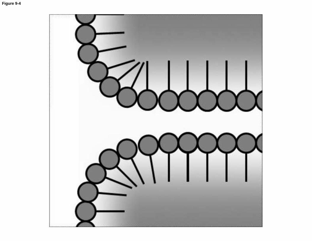
Fig 1 Random, single-ion, and microbeam2 irradiation.
1.3. From random to deterministic
The irradiation technique depends on the required spatial distribution of the ion tracks. Usually ion
tracks are distributed at random. Random tracks are used to study and modify global properties.
Randomness can be an advantage or a disadvantage, depending on the application. In filter applications
the problem of multipore configurations exists and is tackled by wide angle irradiations. Fig 1 (left)
shows a random distribution of about 100 etched cones of 32 µm diameter in glass. At the given nominal
porosity P 0.12 (defined as the product of fluence F and area A of an individual etched track, where F is
the number of ions impinging per unit area), about 14 double and 1 triple track configurations were
formed. Fig 1 center shows an etched channel of 4 µm diameter, fabricated for red blood cell
deformability studies. [17], [28] Fig 1 (right) shows a regular pattern of 15 single pores of about 5 µm
1 Trade name of PGG Industries, http://corporateportal.ppg.com/ppg/
2 Reprinted from Nuclear Instruments and Methods in Physics Research Section B, Vol 260, Fischer, B.E., Heiss, M., A facility to mass-
produce ordered single-hit patterns in continuous 35 mm films, 442-444, Copyright (2007), with permission from Elsevier

1 2 3 4 5 6 7 8 9 10 11 12 13 14 15 16 17 18 19 20 21 22 23 24 25 26 27 28 29 30 31 32 33 34 35 36 37 38 39 40 41 42 43 44 45 46 47 48 49 50 51 52 53 54 55 56 57 58 59 60 61 62 63 64 65
Controlled fabrication of … 4 9-Dec-09
diameter placed at distances of 50 µm. [19] Such irradiations require an ion microbeam and come close to
the ideal of a fully deterministic irradiation. This type of aimed irradiation will not be dealt-with in this
report.
1.4. Alternative techniques
Nanomaterials are being widely used in advanced technologies due to their unique properties
inaccessible by other means. Among the variety of nanomaterials, materials containing nanochannels and
nanowires attract increasing interest. First of all, this is caused by the revolutionary potential of the
resistive-pulse sensing method that can be applied to detect and analyze important biological
macromolecules [29-30]. As the sensitivity of the resistive-pulse technique increases with decreasing pore
diameter and length, numerous approaches have been suggested to produce nanopores in thin foils, which
are presented in recent review papers [31-32]. Another promising application of abiotic nanopores is to
simulate the functions of biological channels formed by transmembrane proteins [33]. Recent studies
performed on synthetic nanopores have provided valuable information on the transport of ions and neutral
particles through the pores as small as some nanometers in diameter [34-35]. The knowledge of physical
mechanisms governing the transport processes on the nanometer scale is expected to lead to integrated
sample preparation and analysis systems [36]. Apart from individual nanopores, nanomaterials prepared
by the so-called membrane based template synthesis [37] are also a subject of research and development
activities in many laboratories. Focused electron and ion beams (FIB) are being used to fabricate pores
down to diameters of a few nanometers [38]. Especially elegant are those methods which allow operating
with a single nanopore or with a preset number of nanopores [38-39]. While FIB is particularly useful for
thin membranes and pores of a few nanometers diameter, the ion track technique provides substantially
higher aspect ratios up to about 104. For building devices with precisely tunable mass transport, the ion
track technique is a good choice because it offers the possibility to control in a wide range both the
number of pores, the pore geometry and the aspect ratio [40].
We would like to highlight here two interesting alternatives to the single-ion fabrication technique,
among which the single contact technique developed at EPFL [41] and the embedded membrane
technique developed at GSI in collaboration with TU Munich [42-43] are most closely related with the
work described here. First, the single contact technique uses multiporous ion track membranes. Both sides
of the membrane are coated with a thin metal film. One metal film serves as cathode, the other metal film
is placed closer to the anode and has a potential floating between anode and cathode potential. The wires
grow at slightly different velocities from the cathode film toward the floating electrode film. As soon as
the fastest growing wire contacts the floating film, its potential drop is used to terminate the electro-
deposition process. In this way exclusively the resistance of the contacted single nanowire can be
measured among numerous semi-completed nanowires. The technique can be applied to multiporous
templates of alumina, polyimide, and polycarbonate. [44] Second, the embedded membrane technique is a
combination of single-ion pores with self-assembled biopores [42]. It uses a large single-ion pore as a
carrier frame to stabilize a lipid bilayer membrane acting as septum in a conductometric cell. One
compartment of the conductometric cell contains subunits of self-assembling biological pores. As soon as
the first pore has been self-assembled, the pore can be used to detect single and double stranded DNA
fragments.
1.5. Goal of this report
The goal of our article is to make the scientific community aware of the special features of single
ion channel fabrication and to demonstrate convincingly the possibility of controlled etching and
electroreplication. We provide here an overview of available equipment and techniques to irradiate, etch
and replicate individual ion tracks and describe the necessary equipment for fabrication of single-ion
track micro- and nanostructures, including irradiation, etching and electroreplication. Etching can be
interrupted as soon as the desired size is reached. The etched channel can be filled with another material

1 2 3 4 5 6 7 8 9 10 11 12 13 14 15 16 17 18 19 20 21 22 23 24 25 26 27 28 29 30 31 32 33 34 35 36 37 38 39 40 41 42 43 44 45 46 47 48 49 50 51 52 53 54 55 56 57 58 59 60 61 62 63 64 65
Controlled fabrication of … 5 9-Dec-09
by electrodeposition. The composition of the deposited material can be programmed and the
electrodeposition can be interrupted at a prescribed wire length or bud diameter. Examples of fabricated
channels and wires resulting from the described apparatus are provided. Our goal is to present the unique
irradiation facilities offered by GSI and Uppsala and to provide a survey of applications in various fields,
ranging from biosensors to spintronic devices.
2. Piercing polymer foils with a preset number of ions
2.1. Ion beam requirements
The energy of the incoming ion must be sufficient to penetrate the vacuum window, the tape, and
the sensitive zone of the detector, whereby the flux density of the ion beam has to be reduced to be able to
switch the ion beam reliably off after the arrival of one or a preset number of ions. Therefore we describe
here the special requirements for preparing an ion beam with sufficiently reduced flux density.
For wide beam irradiations, such as in filter production, the beam is usually swept over the sample
area at full intensity. This is not the case in single ion irradiations where the beam flux density has to be
decreased by several orders of magnitude to ensure sufficient low count rate to switch the beam off after a
precise number of ions have passed through the beam defining aperture and through the target material.
For this purpose, the beam intensity of the accelerator needs to be reduced in steps. First, using a Faraday
cup, the ion beam is decreased to an intensity below 1 particle nA corresponding to the lower limit of
convenient current measurements. Second, using a series of fluorescent screens placed along the beam-
line as monitors, the intensity is decreased by about five orders of magnitude by defocusing the ion beam
while keeping it on the prescribed beam-line axis. We use as fluorescent material Al2O3, CdWO4 and ZnS
with respectively increasing sensitivities. When reaching the lower limit of the most sensitive screen
(ZnS), the detector pulse rate is checked and the defocusing is readjusted to a count rate compatible with
the shutter speed. For single-ion irradiations we use a count rate of typically 10 ions per second. For a
critical aperture of 0.4 mm diameter this corresponds to a flux density of roughly 104 ions cm
-2 s
-1.
2.2. Tape transport system
The compact and mobile tape transport system (shown in Fig 2 and Fig 3) is usually attached to an
ion accelerator (nuclear charge Z above ~18 and specific energy between 1 and 10 MeV/nucleon) but can
in principle be used even with a tiny fission fragment source. In contrast to its precursor, the tape
transport system described here is independent of tape perforations3. The ion penetrates a thin film
vacuum window (4 µm polyethylene terephthalate, PET) separating the accelerator vacuum from the tape
irradiation system which is at ambient pressure. After having detected a preset number of ions, the ion
beam is switched off by an electrostatic deflector, which is part of the accelerator, the tape is marked by a
needle printer and the polymer foil is shifted to a new position. The shutter time has to be short compared
with the average time between ion counting events. A more detailed description is given in the following.
3 The first single-ion irradiation system at GSI used perforated 36 mm films for transport and retrieval of irradiation spots.

1 2 3 4 5 6 7 8 9 10 11 12 13 14 15 16 17 18 19 20 21 22 23 24 25 26 27 28 29 30 31 32 33 34 35 36 37 38 39 40 41 42 43 44 45 46 47 48 49 50 51 52 53 54 55 56 57 58 59 60 61 62 63 64 65
Controlled fabrication of … 6 9-Dec-09
Fig 2 Principle of tape transport system4 consisting of beam deflector, beam diagnostics and tape transport. The
high voltage supply and the beam deflector (left) are integral parts of the ion accelerator.
Fig 3 Perspective view of tape transport system.
4 Left: beam diagnostics. Right: tape transport platform including
a video camera for checking the tape transport, a marking indenter and ion detector (below the indenter). The tape
transport platform can be attached at two fixed angles with respect to the beam axis corresponding to an ion
incidence on the tape of 90º (shown here) and 35º.
2.3. Low flux beam diagnostics
Video camera 1 is mounted inside the vacuum system and serves for observing the fluorescent
screen continuously. The retractable fluorescent screen is the last but most sensitive screen in a series of
three fluorescent screens arranged along the beam-line. It consists of a ZnS based phosphor which was
4 Developed at GSI Darmstadt for use at The Svedberg Laboratory of Uppsala University, Sweden; http://rsp.eunitt.de/ : Projects : Controlled
Fabrication of Micro Channels : thumbnails
Ion
Beam
Retractable Fluorescent
Screen Video Camera 1
Beam Defining Aperture
Electron Repeller
Retractable Faraday
Cup
Vacuum Window
Pristine Tape
Irradiated Tape
Tape Stepper
Beam Deflector
Needle Printer
Ion Detector
Computer
Pulse Amplifier
High Voltage
Video Camera 2

1 2 3 4 5 6 7 8 9 10 11 12 13 14 15 16 17 18 19 20 21 22 23 24 25 26 27 28 29 30 31 32 33 34 35 36 37 38 39 40 41 42 43 44 45 46 47 48 49 50 51 52 53 54 55 56 57 58 59 60 61 62 63 64 65
Controlled fabrication of … 7 9-Dec-09
paint-brushed on its backing plate from a suspension of the phosphor in an aqueous solution of sodium
silicate, which serves as a binder. With this screen it is possible to observe ion beams down to about 103
particles cm-2
s-1
. The center bore of the fluorescent screen permits passing the beam through the electron
repeller onto the retractable Faraday cup. The fluorescent screen has to be protected from rapid fading at
beam intensities above 10 particle pA by retracting it from the ion beam. The electron repeller is used as
the entrance aperture of a Faraday cup. It can be set on negative (repelling) potential with respect to the
Faraday cup to prevent secondary electrons from escaping and falsifying the current measurement. The
Faraday cup can be connected to a current digitizer or a pico-amperemeter and used for calibrating high
beam intensities >100 particle pA. It has to be inserted at high beam intensities to protect the ion detector
from fading. The Faraday cup is withdrawn from the beam when reaching sufficiently low intensity for
being able to use the fluorescent screen. The beam-defining aperture restricts the ion beam to a small spot
on the polymer tape and is covered by a vacuum window consisting of a thin polymer foil (4 µm PET)
attached to it by double adhesive from the outside of the vacuum system. To reduce ion scattering from
the rim of the aperture we use apertures with rather large diameters between 50 and 500 µm.
2.4. Performing an irradiation
The tape transport uses guide rolls with tilted edges to keep the tape centered. The tape is kept
under a defined mechanical tension by counteracting drive motors and its movement is remotely observed
with Video Camera 2. After reaching the preset number of hits, the tape stepper roll pulls the tape to the
next irradiation position. The irradiation points can be placed at preset distances along the axis of the
polymer film. We use frame sizes of typically 25 mm. As ion detector we use a silicon PIN diode from
Hamamatsu5 with an active area of about 4x4 mm
2. In comparison to regular photo diodes, infrared
sensitive PIN diodes have a large depletion depth and can be easily used for ion detection up to ion ranges
between 20 and 30 µm corresponding roughly to specific ion energies between 2 and 3 MeV/nucleon. For
thin tapes with thicknesses d < 50 µm a polymer foil of approximate thickness d’ ~ (50 – d) µm was
placed in front of the tape to reduce the energy of the incident ion. In this way, the PIN diode could be
used as an energy sensitive detector even for thin tapes. The needle printer marks the irradiation spot at
the margin of the tape by an indention visible to the naked eye. After completing the tape irradiation, the
indention is used for punching out circular disks of 18 or 25 mm diameter from the tape, whereby the
punching tool is placed with respect to the indention. In this way circular disks are obtained containing
the required number of ion tracks in their center. Irradiation frames containing the preset number of ion
tracks within a preset pulse height window are marked as good by a broad indent (9 pins). All other
irradiation frames, usually less than 1% of the irradiations, are marked as bad by a 1 pin indent and can be
recognized and discarded during the punching.
Bad irradiations can be the result of shutter delay or random coincidences. They can also result
from particles scattered at the rim of the beam defining aperture, arriving at the detector with reduced
energy. In principle, the probability of bad events can be further suppressed by a coincidence arrangement
consisting of two detectors, a thin film E detector placed before the tape combined with an E detector
placed after the tape. Toward this goal, a thin film E detector was developed by Thungström et al. [45]
and tested but not used hitherto.
The detector signal is fed to an amplifier stage and shaping filter. The electronic system was tested
with a separate PIN diode irradiated by a weak alpha source [6].The pulse height distribution of a tape
irradiation is shown in Fig 4.
5 Si PIN photodiode S1223 series, Hamamatsu Photonics K.K. – Solid-state division, Japan, Cat. No KSPD0001E01, Jan. 2002;
http://www.hamamatsu.com/
6 Cf-252, http://www.ornl.gov/sci/isotopes/r_cf252.html

1 2 3 4 5 6 7 8 9 10 11 12 13 14 15 16 17 18 19 20 21 22 23 24 25 26 27 28 29 30 31 32 33 34 35 36 37 38 39 40 41 42 43 44 45 46 47 48 49 50 51 52 53 54 55 56 57 58 59 60 61 62 63 64 65
Controlled fabrication of … 8 9-Dec-09
Fig 4 Pulse height distribution of single-track detector using
129Xe
27+ ions of 8.3 MeV/nucleon passing through a
window of ca. 4 µm PET and a 30 µm thick PET tape tilted at 35⁰ (total track length ca. 48 µm).
2.5. Digital control system
The tape irradiation is controlled by a Field Programmable Gate Array (FPGA) [16] controlled via
Ethernet from a host computer. The FPGA opens the beam shutter, digitizes the detector pulses,
determines pulse height and counts the pulses. The ion detector is placed as close as possible behind the
polymer film. The detector pulses are amplified by a preamplifier followed by a signal shaper and a fast
analog to digital converter. The signal is amplified and shaped in order to minimize the influence of noise
and pulse tail. After reaching the preset number of pulses, the digital pulse processor closes the beam
shutter and shifts the tape to a new position. The detector efficiency is monitored during the tape
irradiation. Detector degradation is characterized by gradually decreasing pulse height. The effect
becomes important for very high total counts deposited within the irradiated spot on the ion detector. No
apparent detector degradation was found up to 104 pulse counts within a spot size of about 0.5 mm
diameter, corresponding to a fluence of 5106 ions/cm
2.
2.6. User interface
The tape transport is controlled by a LabVIEW7 code
8. A module settings is used for setting the
parameters of a data acquisition card, which provides eight digital input/output lines and two counters. A
module estimates is used to estimate the number of available frames on the tape from the roll diameter
and the tape thickness. The total irradiation time is estimated from the number of frames irradiated per
second and the total number of frames to be irradiated. A module count rate is used for adjusting the
average count rate to a value compatible with the times needed for pulse processing, shutter speed and
transport time. We use typically 10 counts per second for single-ion irradiations. A module pulse shape
permits to view the pulse shape of individual pulses, to adjust pulse amplification and – if necessary – to
add tape thickness for reducing the pulse height to a value compatible with the detector thickness. The
occurrence of coincident events can be minimized by reducing the ion beam intensity. A module irradiate
is used to set the number of ions per frame and the total number of frames to be irradiated. For each
irradiation a record is saved on hard disk.
3. Single ion track etching and replication
3.1. Conductometric system
We use a thermostated, thermally insulated, electrically shielded conductometric cell [46] inspired
by contacts between Dubna and GSI [9] (Fig 5) in connection with a sensitive current amplifier for
controlled etching. The two cell halves are machined of polychlorotrifluoroethylene (PCTFE) with
7 http://www.ni.com
8 http://rsp.eunitt.de : Projects : Controlled fabrication of Micro Channels : Thumbnails : References, Downloads, Links : e-cell Program

1 2 3 4 5 6 7 8 9 10 11 12 13 14 15 16 17 18 19 20 21 22 23 24 25 26 27 28 29 30 31 32 33 34 35 36 37 38 39 40 41 42 43 44 45 46 47 48 49 50 51 52 53 54 55 56 57 58 59 60 61 62 63 64 65
Controlled fabrication of … 9 9-Dec-09
polished flat ends for improved sealing of the membrane and are compressed by a spring loaded
tightening screw. The electrodes and filling/flushing tubes are accessible during operation through a slit.
The electrolyte can be removed automatically after reaching a desired pore diameter / wire length / bud
diameter. The electric current is recorded as function of time and – after calibration – yields a direct
reading of the actual channel diameter / wire length / bud diameter.
Fig 5 Longitudinal section through conductometric cell
9 consisting of two cell halves between which the ion
track membrane is inserted and compressed by a screw. Four filling/flushing tubes and two electrodes are shown.
The cell is heated from the bottom and encased in an electrical shield. The whole assembly is enclosed by a thermal
insulation (not shown).
Leak currents suppressed a compression seal. The electrolyte is maintained at a preset temperature
and the whole assembly is shielded electrically and thermally by a metallic case. Electrodes and flushing
tubes are plugged-in from the top. The growth of the ion track channels is controlled in real-time by
electric current measurements down to the sub nA range. To minimize electrode polarization, a sinusoidal
voltage with amplitudes below 0.1 V is used permitting to determine membrane thickness and channel
diameter.
3.2. Track replication
For electro-replication of the etched ion track channel, the membrane is coated on one side with a
metal electrode and inserted into a modified conductometric cell in which the right chamber is replaced
by a block of copper serving as cathode. The left chamber is filled with an electrolyte containing the
metal or semiconductor ions.
3.3. Computer interface
The principle of the data acquisition system is shown in Fig 6. The computer controls the data
acquisition card, which converts the digital signal from the computer into an analog voltage, which is
applied to the conductometric cell. The output of the conductometric cell is connected with the input of a
pico-amperemeter converting current into voltage. Its output voltage is connected via an analog to digital
converter to the computer. The current through the etched ion track channel is measured and analyzed
using a LabVIEW7 based graphical user interface
10:
9 http://rsp.eunitt.de : Projects : Controlled Fabrication of Micro Channels : thumbnails : E-Cell 2
10 http://rsp.eunitt.de : Projects : Controlled Fabrication of Micro Channels : thumbnails
Compression Screw
Electrodes
Membrane
Filling/Flushing Tube
Heater
Electric Shield
Spring

1 2 3 4 5 6 7 8 9 10 11 12 13 14 15 16 17 18 19 20 21 22 23 24 25 26 27 28 29 30 31 32 33 34 35 36 37 38 39 40 41 42 43 44 45 46 47 48 49 50 51 52 53 54 55 56 57 58 59 60 61 62 63 64 65
Controlled fabrication of … 10 9-Dec-09
Fig 6 Principle of the data acquisition system
11 consisting of a computer, a data acquisition card (DAQ Card
12)
containing one digital to analog converter (DAC) and two analog to digital converters (ADC), the conductometric
cell, and a current amplifier (picoamperemeter).
3.4. User interface
One module defines the parameters of the data acquisition board. The next module selects among
four modes: The normal operation of the system, the optional use of relays for filling or flushing the
electrolyte, the automatic switching between various function generators, and the conditional switching of
the applied output voltage. Another module selects among different output function generators with
arbitrary shape, amplitude, bias, and frequency. A module exists for calibrating the current amplifier. A
module exists for setting the data acquisition parameters, in particular scan rate and time limit of the data
acquisition. It provides two acquisition modes: The dc mode acquires current and voltage as a normal
time series of data points. The lock-in mode requires a periodic output voltage for determining the phase
relation between input voltage and output current. Another module displays the acquired raw data and
stores selected data as a new file. It zooms, averages, compresses, and restricts raw data. The selected
data are passed to an intermediate storage from which they can be accessed by other modules for further
treatment and display. The module can alternatively display all data, only data acquired within a given
time interval, all data from a set time onward, and a chart display showing only the most actual data
points. The density of the displayed data points is automatically adapted to the screen resolution and can
be increased or decreased in steps. Furthermore, a calculation module exists providing a set of
subprograms to determine membrane thickness, track etch rate, channel diameter, and wire diameter. In
addition, it comprises a conditional option for changing the voltage or switching a relay when reaching a
specific threshold. For ion track etching a shape selector exists corresponding to cylindrical, single-cone
and double conical shapes. Its output data can be passed to a display module. The module can be used to
determine membrane thickness, track etch ratio, channel diameter, and wire length.
4. Single-ion track applications
4.1. Etching of single track
Real-time controlled etching was applied to single ion track etching (Fig 7). The example
demonstrates four steps of extracting results from raw data: break-through time, track etch rate, bulk etch
rate, etched track diameter, radius of latent track core (the preferentially etched zone), radius of latent
track halo (the cross-linked part of the latent ion track). Experimental parameters: single ion track
(129
Xe27+
, 8.3 MeV/nucleon) in 30 µm polycarbonate, etched in 5 M NaOH + trace of Dowfax 2A1
surfactant at ca. 50 ⁰C. Applied voltage 10 Hz sine at amplitude 0.1 V.
11 http://rsp.eunitt.de : Projects : Controlled Fabrication of Micro Channels : thumbnails: Data Acquisition
12 National Instruments DAQCard-6062E , http://sine.ni.com/nips/cds/view/p/lang/en/nid/11918

1 2 3 4 5 6 7 8 9 10 11 12 13 14 15 16 17 18 19 20 21 22 23 24 25 26 27 28 29 30 31 32 33 34 35 36 37 38 39 40 41 42 43 44 45 46 47 48 49 50 51 52 53 54 55 56 57 58 59 60 61 62 63 64 65
Controlled fabrication of … 11 9-Dec-09
Fig 7 Etching a single-ion track.
13 (cf. [47-48]) (a) Break-through, followed by a quadratic increase of the electric
current through the etched channel. (b) Channel radius calculated from (a). (c) Radial etch rate versus time
calculated from (b). (d) Radial etch rate versus radius calculated from (b) and (c). [49]
4.2. Etching of 100 tracks
The etching of 100 ion tracks (Fig 8) closely resembles the etching of a single track (Fig 7),
however, as expected, with reduced signal to noise ratio.
13 Reprinted from Radiation Measurements, 43, Reimar Spohr, Real-time control of track etching and recent experiments relevant to micro- and
nano-fabrication, Figs. 5, 6 Copyright (2008), with permission from Elsevier.

1 2 3 4 5 6 7 8 9 10 11 12 13 14 15 16 17 18 19 20 21 22 23 24 25 26 27 28 29 30 31 32 33 34 35 36 37 38 39 40 41 42 43 44 45 46 47 48 49 50 51 52 53 54 55 56 57 58 59 60 61 62 63 64 65
Controlled fabrication of … 12 9-Dec-09
Fig 8 Etching 100 ion tracks
14 (cf. [47-48]). (a) Break-through, followed by a quadratic increase of the electric
current through the etched channel. (b) Channel radius calculated from (a). (c) Radial etch rate versus time
calculated from (b). (d) Radial etch rate versus radius calculated from (b) and (c). [49]
4.3. Probability of double tracks
Assuming a circular beam spot size of radius R with N etched ion tracks of radius r one obtains a
probability for the occurrence of double pores formed by exactly two pores according to
(Eq. 1) PePP 4
2 4 ,
where 2rNP is the nominal porosity. [50] Let us consider the example of 100 ion tracks of 1 µm
diameter placed at random on a circular area of diameter 100 µm. Already about 4 double pores will be
formed on the average, which is a strong argument for single-pore and focused beam experiments, if
double pores are expected to falsify the results.
4.4. Modifying cone angle
Ion track etching is governed by the selective removal of the latent ion track by the etch medium as
compared to the pristine material. [40] Over short distances, in comparison with the total range of the ion
in the solid, the cone half-angle depends on the track etch ratio, which is defined as the ratio of the
track etch rate vt and the bulk etch rate vg according to
14 Reprinted from Radiation Measurements, 43, Reimar Spohr, Real-time control of track etching and recent experiments relevant to micro- and
nano-fabrication, Figs. 5, 6 Copyright (2008), with permission from Elsevier.

1 2 3 4 5 6 7 8 9 10 11 12 13 14 15 16 17 18 19 20 21 22 23 24 25 26 27 28 29 30 31 32 33 34 35 36 37 38 39 40 41 42 43 44 45 46 47 48 49 50 51 52 53 54 55 56 57 58 59 60 61 62 63 64 65
Controlled fabrication of … 13 9-Dec-09
(Eq. 2)
t
g
v
varcsin .
The cone half-angle can be increased either by increasing vg or by decreasing vt. In polymers, vg can be
increased by adding organic solvents to the etching solution, in case of PET and polycarbonate (PC) by
methanol being added to the basic etchant. On the other hand, the track etch rate vt can be decreased by
thermal annealing before etching is started. This, too, will increase the cone half angle . Conical
nanopores are obtained by etching a single ion track membrane from one side only and the asymmetry
can be accentuated by retracting the etch-active OH- ions from the etching tip [22].
4.5. Asymmetric single pores
In polymers containing oxygen in the backbone of the polymer strand, such as PET and PC,
dangling carboxylic groups (R-COOH) are formed on the etched wall and still remain there after flushing
off the etch medium. The resulting charged conical nanopores provide a possibility of current
rectification. Since the effect depends on pH it can be used as a basis for sensor development. The
current-voltage characteristic can be compared with an electrical diode, however, it rather obeys a power
law [34] than an exponential function. The charged groups can be used to attach other groups or
biomolecules to the pore walls. But even covalent bonding can be used for attachment if appropriate
functional groups exist on the etched surface. This is a starting point for biospecific single-channel
sensors [51-60].
4.6. Surfactant assisted etching
Cylindrical tracks are obtained if is very small, i.e. if the track etch rate vt is large in comparison
with the bulk etch rate vg (Eq. 2). In minerals such as mica track etch ratios above 1000 are possible. For
polymers, a special technique was developed at Dubna [61], reducing the surface attack by a monolayer
of surfactant molecules unable to penetrate into the etching zone of the ion track (Fig 9). On this basis,
using as surfactant alkyldiphenyloxide disulfonate (Dowfax 2A1), the shape of the etched pore channel
can be made cylindrical or even cigar-like, as the case requires. The geometry of the pore is governed by
the interplay between protection, attack, and diffusion of both etchant and surfactant molecules. Under
slow etching conditions, the selectivity of ion track etching was increased, leading to nearly cylindrical
channels [62] (Fig 10).
Fig 9 Illustration of surfactant assisted ion track etching.15
(From left to right) The diffusion of the surfactant molecules into the etching zone is delayed by their size. At sufficient channel diameter the molecules are able to penetrate into the etching track channel, where they absorb and delay further etching of the track wall. [62]
15 http://rsp.eunitt.de : Downloads : Ion track experiments for micro and nanofabrication

1 2 3 4 5 6 7 8 9 10 11 12 13 14 15 16 17 18 19 20 21 22 23 24 25 26 27 28 29 30 31 32 33 34 35 36 37 38 39 40 41 42 43 44 45 46 47 48 49 50 51 52 53 54 55 56 57 58 59 60 61 62 63 64 65
Controlled fabrication of … 14 9-Dec-09
Fig 10 Single wire
16 [62]; Copper replica of cylindrical ion track channel, electro deposited at 10 nA maximum
current. Diameter 2.2 μm, length 25.6 μm, bud diameter (visible at bottom) 31±3 μm.
4.7. Magnetoresistance of homogeneous wires
The magnetoresistance of homogeneous magnetic wires depends strongly on the direction of the
applied magnetic field with respect to the wire axis and is termed Anisotropic Magnetic Resistance
(AMR), which obtains its maximum if the magnetic field direction is at 90º with respect to the wire axis.
The anisotropic magnetoresistance ratio, AMR ratio, is defined as MR [%] = 100 (Rmax – Rmin)/Rmin,
where Rmax and Rmin is the resistance at zero and saturation field, respectively. Fig 11 displays the
magnetoresistance curves of a Ni nanowire in a single-channel template with a channel diameter of
(500±50) nm. The AMR curves exhibit the usual dependence on the direction of the applied magnetic
field. In the direction parallel to the wire (0º), the effect of the magnetic field on the resistance is very
small and the MR ratio is almost zero, while in the direction perpendicular to the wire (90º), the MR
effect has a maximum. An AMR ratio of 1.0 % was observed for a Ni nanowire, which is typical of this
system. Without magnetic field, the resistance of a Ni nanowire is 198.2 . Here, length and diameter of
the nanowire are 30 µm and 500 nm, respectively. Therefore, the resistivity is estimated to be around 130
m confirming that the electrodeposited nanowire has metallic state.
Fig 11 Magnetoresistance of a Ni nanowire
17 electrodeposited in a single channel with diameter (500±50) nm.
16 Reprinted from NIM B, 265, n 1, Leo C.T.; Apel, Pavel; Cheung, T.; Westerberg, Lars; Yu, Peter K.N.; Zet, Cristian; Spohr, Reimar;
Influence of a surfactant on single ion track etching. Preparing and manipulating individual cylindrical micro wires, p 621–625, Copyright 2007, with permission from Elsevier.
17 With kind permission from Springer Science+Business Media: J Appl Electrochem, 38, 2008, 713–719, T. Ohgai, K. Hjort, R. Spohr, R.
Neumann, figure 8-9
1 2 3 4 5 6 7 8 9 10 11 12 13 14 15 16 17 18 19 20 21 22 23 24 25 26 27 28 29 30 31 32 33 34 35 36 37 38 39 40 41 42 43 44 45 46 47 48 49 50 51 52 53 54 55 56 57 58 59 60 61 62 63 64 65
Controlled fabrication of … 15 9-Dec-09
4.8. Magnetoresistance of layered wires
Electro-deposition is a technique for selective deposition of metals according to their electro-
negativity, such as the “standard electrode potential”. Pulsed current electro-deposition can be applied to
obtain a metallic multilayered structure. If the electrode voltage is switched between two levels, one
obtains metal deposits differing on the basis of their electro-negativity. A mixed electrolyte, containing
copper as well as cobalt ions, deposits pure copper at low deposition voltage and an alloy of copper and
cobalt at high deposition voltage. If the electrolyte contains a large fraction of cobalt, the resulting alloy
contains predominantly cobalt and is magnetic. Neighboring magnetic layers can have parallel or anti-
parallel magnetic orientation. The orientation and electric resistance of the multilayer wire depends on the
applied external magnetic field. The magnetic orientation of thin layers can be flipped by spin-polarized
electrons from the next layer. This opens a route to spin-dependent devices [63-64].
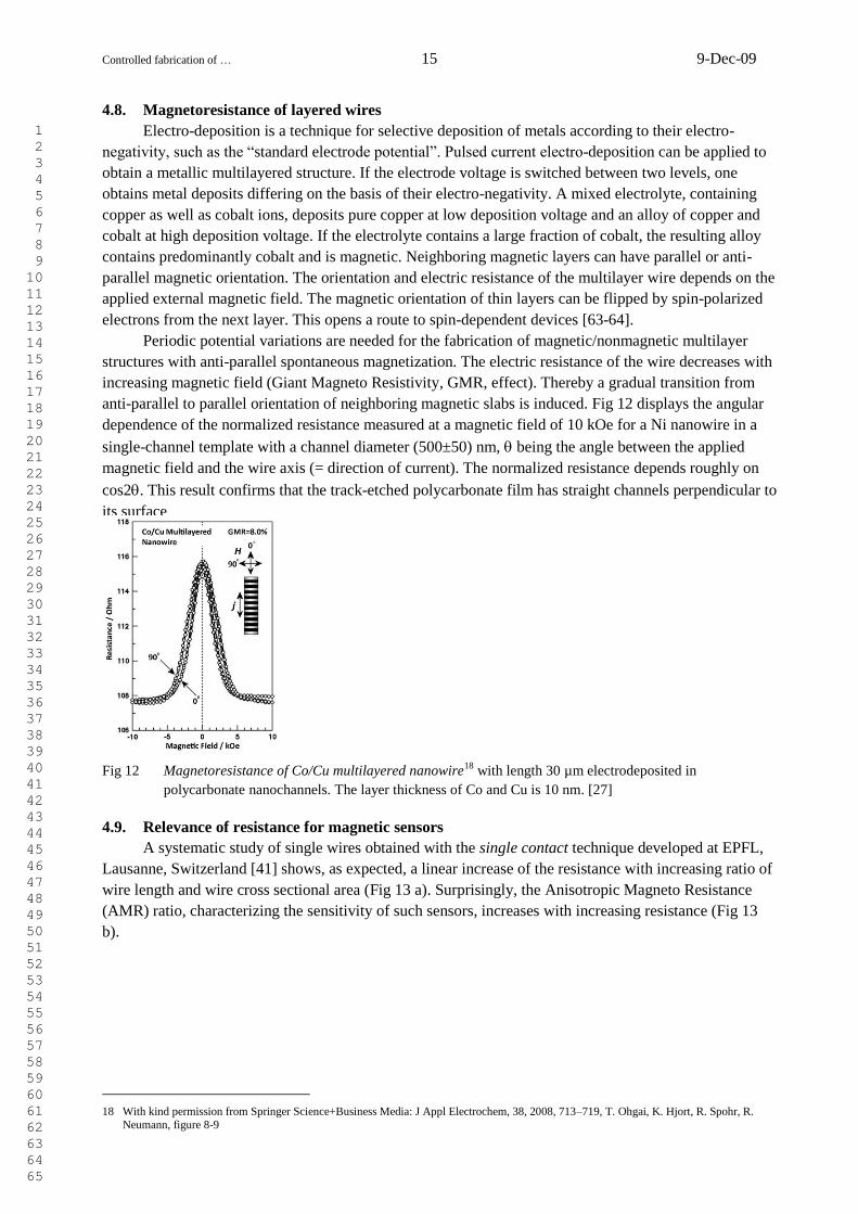
Periodic potential variations are needed for the fabrication of magnetic/nonmagnetic multilayer
structures with anti-parallel spontaneous magnetization. The electric resistance of the wire decreases with
increasing magnetic field (Giant Magneto Resistivity, GMR, effect). Thereby a gradual transition from
anti-parallel to parallel orientation of neighboring magnetic slabs is induced. Fig 12 displays the angular
dependence of the normalized resistance measured at a magnetic field of 10 kOe for a Ni nanowire in a
single-channel template with a channel diameter (500±50) nm, being the angle between the applied
magnetic field and the wire axis (= direction of current). The normalized resistance depends roughly on
cos2. This result confirms that the track-etched polycarbonate film has straight channels perpendicular to
its surface
Fig 12 Magnetoresistance of Co/Cu multilayered nanowire18
with length 30 µm electrodeposited in
polycarbonate nanochannels. The layer thickness of Co and Cu is 10 nm. [27]
4.9. Relevance of resistance for magnetic sensors
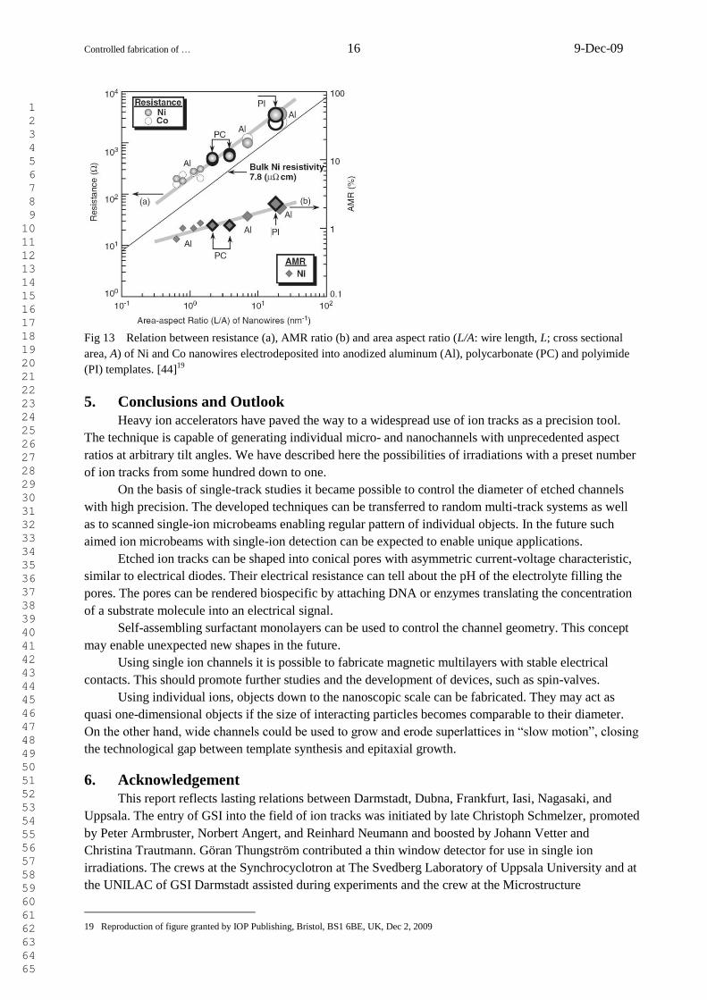
A systematic study of single wires obtained with the single contact technique developed at EPFL,
Lausanne, Switzerland [41] shows, as expected, a linear increase of the resistance with increasing ratio of
wire length and wire cross sectional area (Fig 13 a). Surprisingly, the Anisotropic Magneto Resistance
(AMR) ratio, characterizing the sensitivity of such sensors, increases with increasing resistance (Fig 13
b).
18 With kind permission from Springer Science+Business Media: J Appl Electrochem, 38, 2008, 713–719, T. Ohgai, K. Hjort, R. Spohr, R.
Neumann, figure 8-9
1 2 3 4 5 6 7 8 9 10 11 12 13 14 15 16 17 18 19 20 21 22 23 24 25 26 27 28 29 30 31 32 33 34 35 36 37 38 39 40 41 42 43 44 45 46 47 48 49 50 51 52 53 54 55 56 57 58 59 60 61 62 63 64 65
Controlled fabrication of … 16 9-Dec-09
Fig 13 Relation between resistance (a), AMR ratio (b) and area aspect ratio (L/A: wire length, L; cross sectional
area, A) of Ni and Co nanowires electrodeposited into anodized aluminum (Al), polycarbonate (PC) and polyimide
(PI) templates. [44]19
5. Conclusions and Outlook
Heavy ion accelerators have paved the way to a widespread use of ion tracks as a precision tool.
The technique is capable of generating individual micro- and nanochannels with unprecedented aspect
ratios at arbitrary tilt angles. We have described here the possibilities of irradiations with a preset number
of ion tracks from some hundred down to one.
On the basis of single-track studies it became possible to control the diameter of etched channels
with high precision. The developed techniques can be transferred to random multi-track systems as well
as to scanned single-ion microbeams enabling regular pattern of individual objects. In the future such
aimed ion microbeams with single-ion detection can be expected to enable unique applications.
Etched ion tracks can be shaped into conical pores with asymmetric current-voltage characteristic,
similar to electrical diodes. Their electrical resistance can tell about the pH of the electrolyte filling the
pores. The pores can be rendered biospecific by attaching DNA or enzymes translating the concentration
of a substrate molecule into an electrical signal.
Self-assembling surfactant monolayers can be used to control the channel geometry. This concept
may enable unexpected new shapes in the future.
Using single ion channels it is possible to fabricate magnetic multilayers with stable electrical
contacts. This should promote further studies and the development of devices, such as spin-valves.
Using individual ions, objects down to the nanoscopic scale can be fabricated. They may act as
quasi one-dimensional objects if the size of interacting particles becomes comparable to their diameter.
On the other hand, wide channels could be used to grow and erode superlattices in “slow motion”, closing
the technological gap between template synthesis and epitaxial growth.
6. Acknowledgement
This report reflects lasting relations between Darmstadt, Dubna, Frankfurt, Iasi, Nagasaki, and
Uppsala. The entry of GSI into the field of ion tracks was initiated by late Christoph Schmelzer, promoted
by Peter Armbruster, Norbert Angert, and Reinhard Neumann and boosted by Johann Vetter and
Christina Trautmann. Göran Thungström contributed a thin window detector for use in single ion
irradiations. The crews at the Synchrocyclotron at The Svedberg Laboratory of Uppsala University and at
the UNILAC of GSI Darmstadt assisted during experiments and the crew at the Microstructure
19 Reproduction of figure granted by IOP Publishing, Bristol, BS1 6BE, UK, Dec 2, 2009

1 2 3 4 5 6 7 8 9 10 11 12 13 14 15 16 17 18 19 20 21 22 23 24 25 26 27 28 29 30 31 32 33 34 35 36 37 38 39 40 41 42 43 44 45 46 47 48 49 50 51 52 53 54 55 56 57 58 59 60 61 62 63 64 65
Controlled fabrication of … 17 9-Dec-09
Laboratory (Ångström Laboratory, Uppsala University) in using advanced equipment. Klas Hjort
(Materials Science, Ångström Laboratory, Uppsala University) stimulated the described tape transport
system in the frame of the European Research Training Network No HPRN-CT-2000-00047. This work
was supported by the Wenner Gren Foundation, Stockholm (Sweden).
References
[1] R.L. Fleischer, P. B. Price, R.M. Walker; Nuclear tracks in solids: principles and applications; University of
California Press, Berkeley, 1975. http://www.ion-tracks.de/nuc/index.html
[2] P.B. Price, G.M. Comstock, R.L. Fleischer, W.R. Giard, H.R. Hart and G.E. Nichols; Cosmic-ray tracks in
plastics: The Apollo helmet dosimetry experiment.; Science 172 (1971) 154 .
[3] D.A. Young; Etching of radiation damage in lithium fluoride; Nature 182 (1958) 375-377
[4] R.L. Fleischer, P.B. Price and R.M. Walker; Method of forming fine holes of near atomic dimensions; Rev.
Sci. Instr. 34 (1963) 510-512
[5] R.L. Fleischer, P.B. Price and E.M. Symes; Novel filter for biological materials; Science 143 (1964) 249-
250.
[6] R.W. DeBlois, C.P. Bean; Counting and sizing of submicron particles by the resistive pulse technique;
Review of Scientific Instruments 41 (1970) 909-916.
[7] G.E. Possin; A method for forming very small diameter wires; Rev. Sci. Instrum. 41 (1970) 772-774
[8] Early reports on cyclotron irradiations at Dubna performed by V.P. Perelygin and G.N. Flerov date back to
around 1970.
[9] P.Yu. Apel, A.Yu. Didyk, V.I. Kuznetsov; Production of single heavy-ion tracks in polymers; Instruments
and Experimental Techniques 31 (1988) 1418-1420, ISSN: 0020-4412.
[10] V. I. Kuznetsov, A.Y. Didyk, P.Y. Apel; Production and investigation of nuclear track membranes at JINR;
Nucl. Tracks Radiat. Meas. 19 (1991) 919-924.
[11] E. J. van Veldhuizen, C.G. Granqvist, K. Hjort, G. Niklasson, C.G. Ribbing, G. Thornell, L. Nilsson, L.
Westerberg, V. Ziemann, J. Thomas; Materials science applications of heavy ion beams; Proceedings of the
European Particle Accelerator Conference (EPAC’98, IoP Publishing) (1998) 2460
[12] R. Spohr; Nuclear track irradiations at GSI; Nuclear Tracks 4 (1980) 101-108.
[13] R. Spohr; Method and device to generate a predetermined number of ion tracks; German Patent DE 2951376
C2 (1979).
[14] C. Zet, H. Kiesewetter, M. Skoczylas, L. Westerberg, R. Spohr; A system for irradiating polymer films with a
preset number of ions; GSI Scientific Report (2003) 154-154.
[15] C. Zet, C. Fosalau, M. Skoczylas, H. Kiesewetter, R. Spohr; A system for irradiating polymer films with a
preset number of ions ; SIELMEN (2003) 167-170.
[16] C. Zet, R. Spohr; FPGA based digital processor for ion irradiation systems; Bulletin of the Polytechnical
Institute of Iasi, 52 (2006) 933-942 (ISSN 1223-8139)
[17] H.G. Roggenkamp, H. Kiesewetter, R. Spohr, U. Dauer, L.C. Busch; Production of single pore membranes
for the measurement of red blood cell deformability; Biomedizinische Technik 26 (1981) 167-169
[18] B.E. Fischer; The heavy ion microprobe at GSI - used for single ion micromechanics; NIM B 30 (1988) 284-
288
[19] B.E. Fischer, M. Heiss; A facility to mass-produce ordered single-hit patterns in continuous 35 mm films ;
Nuclear Instruments and Methods in Physics Research Section B 260 (2007) 442-444
[20] J.P. Pekola, J.C. Davis, Zhu Yu-Qun, R.N.R. Spohr, P.B. Price, R.E. Packard; Suppression of the critical
current and the superfluid transition temperature of 3He in a single submicon cylindrical channel; Journal of
Low Temperature Physics, 67 (1987) 47-63.
[21] C. Trautmann, R. Spohr, J. Vetter, G. Eska, Y. Hirayoshi; Search for superfluid Josephson effect; Nucl.
Tracks Radiat. Meas., 19 (1991) 967-970.
[22] P.Y. Apel, Y.E. Korchev, Z. Siwy, R. Spohr, M. Yoshida; Diode-like single-ion track membrane prepared by
electro-stopping; Nucl. Instrum. Methods Phys. Res., Sect. B 184 (2001) 337-346.
[23] Z. Siwy, P. Apel, D. Dobrev, R. Neumann, R. Spohr, C. Trautmann, K. Voss; Ion transport through
asymmetric nanopores prepared by ion track etching; Nuclear Instruments & Methods in Physics Research,
Section B: Beam Interactions with Materials and Atoms 208 (2003) 143-148.
1 2 3 4 5 6 7 8 9 10 11 12 13 14 15 16 17 18 19 20 21 22 23 24 25 26 27 28 29 30 31 32 33 34 35 36 37 38 39 40 41 42 43 44 45 46 47 48 49 50 51 52 53 54 55 56 57 58 59 60 61 62 63 64 65
Controlled fabrication of … 18 9-Dec-09
[24] T. Ohgai, L. Gravier, X. Hoffer, M. Lindeberg, K. Hjort, R. Spohr, J.P. Ansermet; Template synthesis and
magnetoresistance property of Ni and Co single nanowires electrodeposited into nanopores with a wide range
of aspect ratios; Journal of Physics D (Applied Physics) 36 (2003) 3109-3114.
[25] T. Ohgai, I. Enculescu, C. Zet, L. Westerberg, K. Hjort, R. Spohr, R. Neumann; Magneto-sensitive nickel
nanowires fabricated by electrodeposition into multi- and single-ion track templates. Journal of Applied
Electrochemistry 36 (2006) 1157-1162
[26] I. Enculescu, M.E. Toimil-Molares, C. Zet, M. Daub, L. Westerberg, R. Neumann, R. Spohr; Current
perpendicular to plane single-nanowire GMR sensor; Applied Physics A (Materials Science Processing) A 86
(2007) 43-47.
[27] T. Ohgai, K. Hjort, R. Spohr, R. Neumann; Electrodeposition of cobalt based ferro-magnetic metal nanowires
in polycarbonate films with cylindrical nanochannels fabricated by heavy-ion-track etching; J Appl
Electrochem 38 (2008) 713–719.
[28] http://ion-tracks.de : Picture gallery : Track etching
[29] K. Healy; Nanopore-based single-molecule DNA analysis. Nanomedicine 2 (2007) 459-481.
[30] E.A. Heins, Z.S. Siwy, L.A. Baker, C.R. Martin; Detecting single porphyrin molecules in a conically shaped
synthetic nanopore. Nano Letters 5 (2005) 1824-1829.
[31] K. Healy, B. Schiedt, A.P. Morrison; Solid-State nanopore technologies for nanopore based DNA analysis.
Nanomedicine 2 (2007) 875-897
[32] C. Dekker; Solid-state nanopores. Nature Nanotechnology 2 (2007) 209-215
[33] M. Ali, B. Schiedt, K. Healy, R. Neumann, W. Ensinger; Modifying the surface charge of single track-etched
conical nanopores in polyimide. Nanotechnology 19 (2008) 085713-085719
[34] Z. Siwy; Ion-current rectification in nanopores and nanotubes with broken symmetry. Adv. Function. Mat. 16
(2006) 735-746.
[35] Y. Choi, L.A. Baker, H. Hillebrenner, C.R. Martin; Biosensing with conically shaped nanopores and
nanotubes. Phys. Chem. Chem. Phys. 8 (2006) 4976-4988.
[36] R. Schoch, J. Han, P. Renaud; Transport phenomena in nanofluidics. Rev. Mod. Phys. 80 (2008) 839-883
[37] C.R. Martin; Nanomaterials: a membrane-based synthetic approach. Science, 266 (1994) 1961
[38] T. Schenkel, V. Radmilovic, E.A. Stach, S.-J. Park, A. Persaud; Formation of a few nanometer wide holes in
membranes with a dual beam focused ion beam system; Journal of Vacuum Science & Technology B 21
(2003) 2720-2723
[39] D.J. Stokes, L. Roussel, O. Wilhelmi, L.A. Giannuzzi, D.H.W. Hubert; Recent advances in FIB technology
for nano-prototyping and nano-characterisation. Ion-Beam-Based Nanofabrication Symposium (2007) 15-20
[40] R. Spohr; Status of ion track technology – prospects of single tracks; Radiation Measurements 40 (2005)
191-202
[41] A. Fabian, C. Terrier, S.S. Guisan, X. Hoffer, M. Dubey, L. Gravier, J.P. Ansermet, J.E. Wegrowe; Current-
induced two-level fluctuations in pseudo-spin-valve (Co/Cu/Co) nanostructures. ; Physical Review Letters 91
(2003) 257209
[42] N. Fertig, C. Meyer, R.H. Blick, C. Trautmann, J.C. Behrends; Microstructured glass chip for ion-channel
electrophysiology; Phys. Rev. E 64 (2001) 040901-040904.
[43] N. Fertig, R.H. Blick, J.C. Behrends; Whole cell patch clamp recording performed on a planar glass chip;
Biophysical Journal 82 (2002) 3056–3062.
[44] T. Ohgai, L. Gravier, X. Hoffer, M. Lindeberg, K. Hjort, R. Spohr, J.P. Ansermet; Template synthesis and
magnetoresistance property of Ni and Co single nanowires electrodeposited into nanopores with a wide range
of aspect ratios; J. Phys. D: Appl. Phys. 36 (2003) 3109–3114
[45] G.G. Thungström, L. Westerberg, R. Spohr, C.S. Petersson; Fabrication and characterization of thin ΔE
detectors for spectroscopic application; Nuclear Instruments & Methods in Physics Research, Section A
(Accelerators, Spectrometers, Detectors and Associated Equipment) 546 (2005) 312-318.
[46] R. Spohr, P.Y. Apel, H. Kiesewetter, M. Skoczylas, C. Zet; Elektrolytische Zellenanordnung; German Patent
Office Munich DE102005020734B3, issued 19.10.2006.
[47] P.Y. Apel, G. Pretzsch; Investigation of the radial pore-etching rate in a plastic track detector as a function of
the local damage density around the ion path; Nuclear Tracks and Radiation Measurements 11 (1986) 45-53.
[48] L. I. Samoilova, P.Y. Apel; Etching of small pores in PETP by different alkalis ; Radiation Measurements 25
(1995) 717-720.

1 2 3 4 5 6 7 8 9 10 11 12 13 14 15 16 17 18 19 20 21 22 23 24 25 26 27 28 29 30 31 32 33 34 35 36 37 38 39 40 41 42 43 44 45 46 47 48 49 50 51 52 53 54 55 56 57 58 59 60 61 62 63 64 65
Controlled fabrication of … 19 9-Dec-09
[49] R. Spohr; Real-time control of track etching and recent experiments relevant to micro and nano fabrication.
Radiat. Meas. 43 (2008) 560-570.
[50] C. Riedel, R. Spohr; Statistical Properties of Etched Nuclear Tracks. I. Analytical theory and computer
simulation; Radiation Effects 42 (1979) 69-75
[51] J.D. Uram, K. Ke, A.J. Hunt, M. Mayer; Label-free affinity assays by rapid detection of immune complexes
in submicrometer pores. Angewandte Chemie, 45 (2006) 2281-2285
[52] Z. Siwy, L. Trofin, P. Kohli, L.A. Baker, C. Trautmann, C.R. Martin; Protein biosensors based on
biofunctionalized conical gold nanotubes; Journal of the American Chemical Society 127 (2005) 5000-5001
[53] M. Ali, B. Schiedt, R. Neumann, W. Ensinger; Biosensing with functionalized single asymmetric polymer
nanochannels; Submitted to Macromol Biosci. 2009 Aug 14. (Epub ahead of print).
[54] H. Bayley, C.R. Martin; Resistive-pulse sensing - from microbes to molecules; Chemical Reviews 100
(2000) 2575-2594.
[55] L.T. Sexton, L.P. Horne, S.A. Shernill, G.W. Bishop, L.A. Baker, C.R. Martin; Resistive-pulse studies of
proteins and protein antibody complexes using a conical nanotube sensor. JACS 129 (2007) 1314713152
[56] J.H. Wang, C.R. Martin; A new drug-sensing paradigm based on ion-current rectification in a conically
shaped nanopore. Nanomedicine 3 (2008) 13-20
[57] M. Ali, B. Yameen, R. Neumann, W. Ensinger, W. Knoll, O. Azzaroni; Biosensing and supramolecular
bioconjugation in single conical polymer nanochannels. Facile incorporation of biorecognition elements into
nanoconfined geometries. JACS 130 (2008) 16351-16357
[58] C.C. Harrell, Z.S. Siwy, C.R. Martin; Conical nanopore membranes: controlling the nanopore shape; Small 2
(2006) 194-198
[59] L.T. Sexton, L.P. Horne, C.R. Martin; Developing synthetic conical nanopores for biosensing applications
[60] M. Ali, P. Ramirez, S. Mafe, R. Neumann, W. Ensinger; A pH-tunable nanofluidic diode with a broad range
of rectifying properties; Nano 3 (2009) 603–608
[61] P.Y. Apel, I. V. Blonskaya, A.Y. Didyk, S.N. Dmitriev, O.L. Orelovitch, D. Root, L.I. Samoilova, V.A.
Vutsadakis; Surfactant-enhanced control of track-etch pore morphology; Nucl. Instrum. Methods Phys. Res.,
Sect. B 179 (2001) 55-62
[62] L.C.T. Man, P.Y. Apel, T. Cheung, L. Westerberg, P.K.N. Yu, C. Zet, R. Spohr; Influence of a surfactant on
single ion track etching. Preparing and manipulating individual cylindrical micro wires; Nucl. Instrum.
Methods Phys. Res., Sect. B 265 (2007) 621–625.
[63] B. Doudin, J.P. Ansermet; Nanostructuring materials for spin electronics; Europhys. News 28 (1997) 14-17.
[64] D. Kelly, J.E. Wegrowe, Trong-kha Truong, X. Hoffer, J.P. Ansermet; Spin-polarized current-induced
magnetization reversal in single nanowires ; Phys. Rev. B 68 (2003) 134425.